

Page 1
March 1997
MWS5101,
MWS5101A
256-Word x 4-Bit
LSI Static RAM
Features
• Industry Standard Pinout
• Very Low Operating Current. . . . . . . . . . . . . . . . . . 8mA
at V
= 5V and Cycle Time = 1µs
DD
• Two Chip Select Inputs Simple Memory Expansion
• Memory Retention for Standby. . . . . . . . . . . . . 2V (Min)
Battery Voltage
• Output Disable for Common I/O Systems
• Three-State Data Output for Bus Oriented Systems
• Separate Data Inputs and Outputs
• TTL Compatible (MWS5101A)
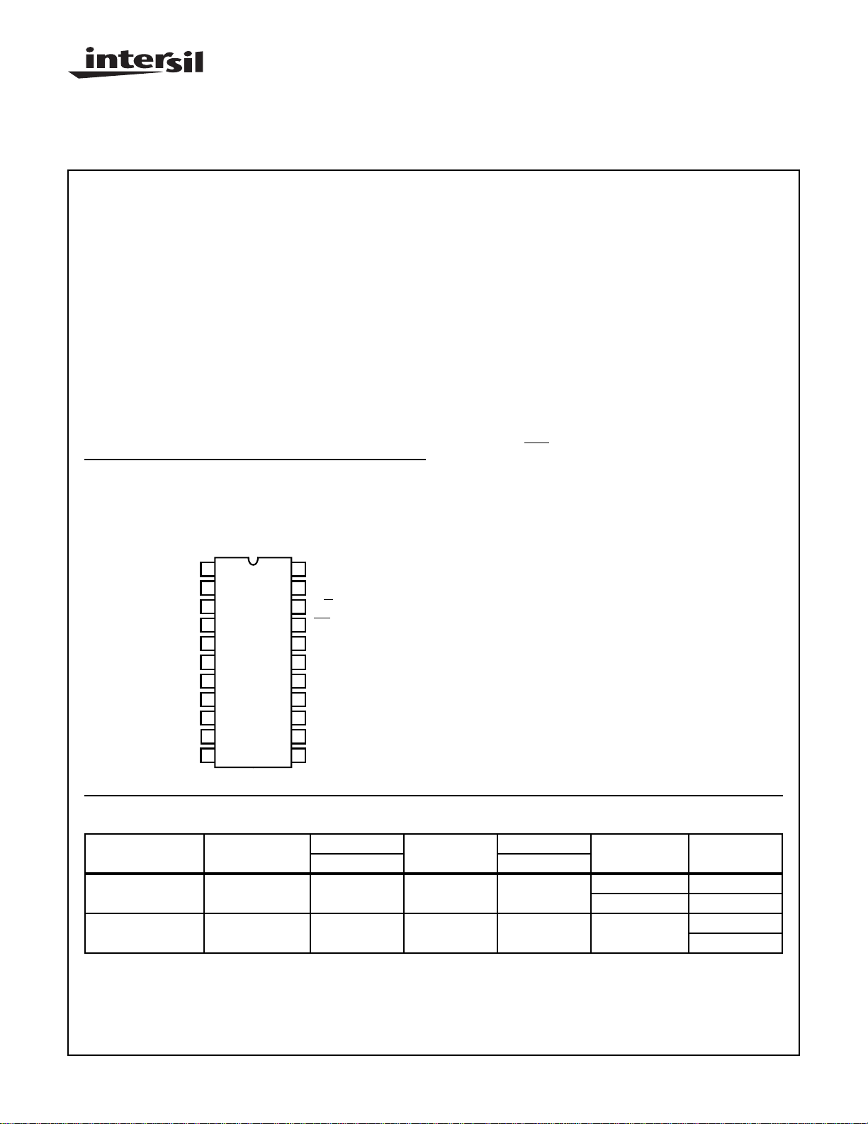
Pinout
MWS5101, MWS5101A
(PDIP, SBDIP)
TOP VIEW
V
A3
A2
A1
A0
A5
A6
A7
V
SS
DI1
DO1
DI2
1
2
3
4
5
6
7
8
9
10
11
22
DD
A4
21
R/
W
20
CSI
19
O.D.
18
CS2
17
DO4
16
DI4
15
DO3
14
DI3
13
DO2
12
Description
The MWS5101 and MWS5101A are 256 word by 4-bit static
random access memories designed for use in memory
systems where high speed, very low operating current, and
simplicity in use are desirable. They have separate data
inputs and outputs and utilize a single power supply of 4V to
6.5V. The MWS5101 and MWS5101A differ in input voltage
characteristics (MWS5101A is TTL compatible).
Two Chip Select inputs are provided to simplify system
expansion. An Output Disable control provides Wire-OR
capability and is also useful in common Input/Output
systems by forcing the output into a high impedance state
during a write operation independent of the Chip Select input
condition. The output assumes a high impedance state
when the Output Disable is at high level or when the chip is
deselected by
The high noise immunity of the CMOS technology is
preserved in this design. For TTL interfacing at 5V operation,
excellent system noise margin is preserved by using an
external pull-up resistor at each input.
For applications requiring wider temperature and operating
voltage ranges, the mechanically and functionally equivalent
static RAM, CDP1822 may be used.
The MWS5101 and MWS5101A types are supplied in 22
lead hermetic dual-in-line, sidebrazed ceramic packages (D
suffix), in 22 lead dual-in-line plastic packages (E suffix), and
in chip form (H suffix).
CS1 and/or CS2.
Ordering Information
MWS5101
PACKAGE TEMP. RANGE
PDIP
Burn-In
SBDIP
Burn-In
CAUTION: These devices are sensitive to electrostatic discharge; follow proper IC Handling Procedures.
http://www.intersil.com or 407-727-9207
0oC to +70oC MWS5101EL2 MWS5101ELS MWS5101AEL2 MWS5101AEL3 E22.4
0oC to +70oC - MWS5101DL3X - MWS5101ADL3 D22.4A
| Copyright © Intersil Corporation 1999
350ns
6-56
MWS5101A
350ns PKG. NO.250ns 250ns
MWS5101AEL3X E22.4
D22.4A
File Number 1106.2
Page 2
MWS5101, MWS5101A
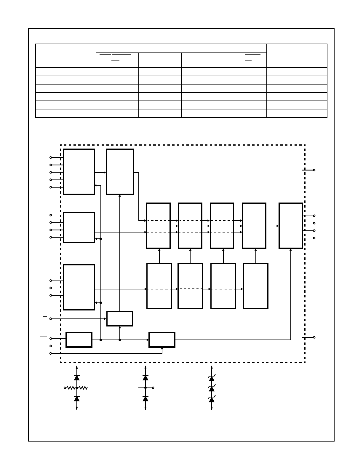
OPERATIONAL MODES
INPUTS
MODE
CHIP SELECT 1
(CS1)
CHIP SELECT 2
(CS2)
OUTPUT
DISABLE (OD)
READ/WRITE
(R/W)
OUTPUT
Read 0101Read
Write 0100Data In
Write 0110High Impedance
Standby 1 X X X High Impedance
Standby X 0 X X High Impedance
Output Disable X X 1 X High Impedance
NOTE: Logic 1 = High, Logic 0 = Low, X = Don’t Care.
Functional Block Diagram
†
A0
A1
A2
A3
A4
4
†
3
†
2
†
1
†
21
(5)
INPUT
BUFFERS
AND
ALL ROWS
DESELECT
FUNCTION
(32)
ROW
DECODERS
†††
22
V
DD
DI1
DI2
DI3
DI4
A5
A6
A7
R/W
CSI
CS2
OD
†
9
†
11
†
13
†
15
†
5
†
6
†
7
†
20
†
19
†
17
†
18
(4)
GATES
(3)
INPUT
BUFFERS
AND
ALL COLUMNS
DESELECT
FUNCTION
CONTROL
A
V
DD
CONTROL
B
(8 x 32)
STORAGE
ARRAY
BIT (1)
(8)
COLUMN
DECODERS
CONTROL
C
V
DD
(8 x 32)
STORAGE
ARRAY
BIT (2)
(8)
COLUMN
DECODERS
(8 x 32)
STORAGE
ARRAY
BIT (3)
(8)
COLUMN
DECODERS
V
DD
(8 x 32)
STORAGE
ARRAY
BIT (4)
(8)
COLUMN
DECODERS
BITS
(1-4)
(4)
BUFFER
DRIVERS
††
10
D01
††
12
D02
††
14
D03
††
16
D04
†††
8
V
SS
V
SS
INPUT PROTECTION
† †† †††
NETWORK
V
SS
OUTPUT
PROTECTION
CIRCUIT
6-57
V
SS
OVER VOLTAGE
PROTECTION
CIRCUIT
Page 3
MWS5101, MWS5101A
Absolute Maximum Ratings Thermal Information
DC Supply Voltage Range, (VDD)
(All Voltages Referenced to VSS Terminal). . . . . . . . -0.5V to +7V
Input Voltage Range, All Inputs . . . . . . . . . . . . . -0.5V to VDD +0.5V
DC Input Current, Any One Input. . . . . . . . . . . . . . . . . . . . . . . . .±10mA
Thermal Resistance (Typical) θJA (oC/W) θJC (oC/W)
PDIP Package. . . . . . . . . . . . . . . . . . . 75 N/A
SBDIP Package. . . . . . . . . . . . . . . . . . 80 21
Operating Temperature Range (TA)
Package Type D. . . . . . . . . . . . . . . . . . . . . . . . . .-55oC to +125oC
Package Type E. . . . . . . . . . . . . . . . . . . . . . . . . . .-40oC to +85oC
Maximum Storage Temperature Range (T
Maximum Junction Temperature
Ceramic Package . . . . . . . . . . . . . . . . . . . . . . . . . . . . . . . +175oC
Plastic Package. . . . . . . . . . . . . . . . . . . . . . . . . . . . . . . . .+150oC
Maximum Lead Temperature (During Soldering)
At distance 1/16 ±1/32 In. (1.59 ±0.79mm)
from case for 10s max. . . . . . . . . . . . . . . . . . . . . . . . . . . .+265oC
) . . .-65oC to +150oC
STG
Recommended Operating Conditions At T
= Full Package Temperature Range. For maximum reliability, operating conditions
A
should be selected so that operation is always within the following ranges:
LIMITS
PARAMETER
UNITSMIN MAX
DC Operating Voltage Range 4 6.5 V
Input Voltage Range V
Static Electrical Specifications At T
= 0oC to +70oC, VDD = 5V ±5%
A
SS
V
DD
CONDITIONS LIMITS
MWS5101 MWS5101A
PARAMETER SYMBOL
Quiescent Device
L2 Types I
DD
V
(V)
- 0, 5 - 25 50 - 25 50 µA
V
O
IN
(V)
MIN
(NOTE 1)
TYP MAX MIN
(NOTE 1)
TYP MAX
Current
L3 Types - 0, 10 - 100 200 - 100 200 µA
Output Low (Sink) Current I
Output High (Source) Current I
Output Voltage Low-Level V
Output Voltage High-Level V
Input Low Voltage V
Input High Voltage V
Input Leakage Current I
Operating Current (Note 2) I
Three-State Output
L2 Types I
OL
OH
OL
OH
IL
IH
IN
DD1
OUT
0.4 0, 5 2 4 - 2 4 - mA
4.6 0, 5 -1 -2 - -1 -2 - mA
- 0, 5 - 0 0.1 - 0 0.1 V
- 0, 5 4.9 5 - 4.9 5 - V
- - - - 1.5 - - 0.65 V
- - 3.5 - - 2.2 - - V
- 0, 5 - - ±5- - ±5 µA
- 0, 5 - 4 8 - 4 8 mA
0, 5 0, 5 - - ±5- -±5 µA
Leakage Current
L3 Types 0, 5 0, 5 - - ±5- -±5 µA
V
UNITS
Input Capacitance C
Output Capacitance C
IN
OUT
NOTES:
1. Typical values are for TA = +25oC and nominal VDD.
2. Outputs open circuited; Cycle time = 1µs.
- - - 5 7.5 - 5 7.5 pF
- - - 10 15 - 10 15 pF
6-58
Page 4

MWS5101, MWS5101A
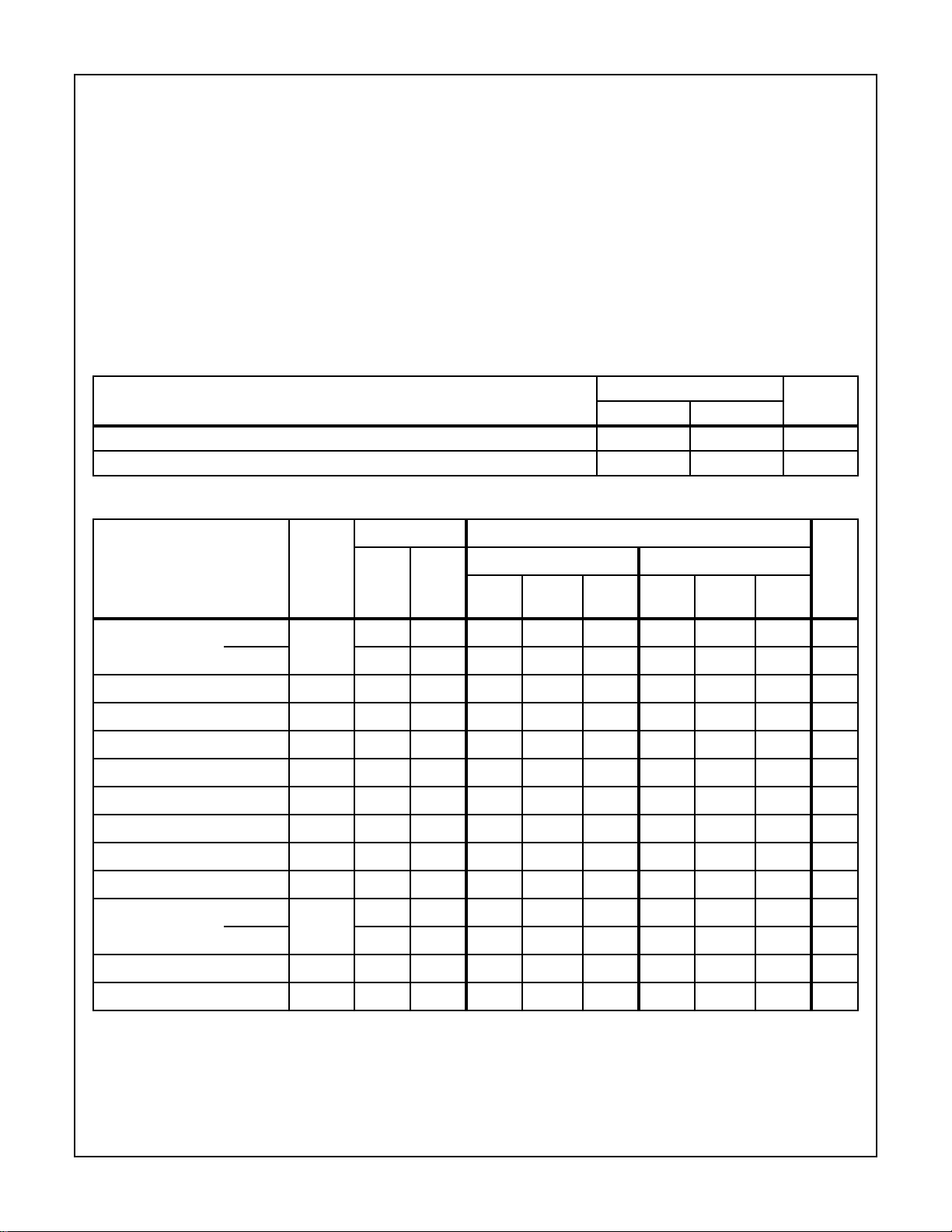
Dynamic Electrical Specifications at T
= 0oC to +70oC, VDD = 5V ±5%
A
LIMITS (NOTE 1)
L2 TYPES L3 TYPES
PARAMETER SYMBOL
(NOTE 2)
MIN
(NOTE 3)
TYP MAX
(NOTE 2)
MIN
(NOTE 3)
TYP MAX
UNITS
READ CYCLE TIMES (FIGURE 1)
Read Cycle t
Access from Address t
Output Valid from Chip Select 1 t
Output Valid from Chip Select 2 t
Output Valid from Output Disable t
Output Hold from Chip Select 1 t
Output Hold from Chip Select 2 t
Output Hold from Output Disable t
RC
AA
DOA1
DOA2
DOA3
DOH1
DOH2
DOH3
250 - - 350 - - ns
- 150 250 - 200 350 ns
- 150 250 - 200 350 ns
- 150 250 - 200 350 ns
- - 110 - - 150 ns
20 - - 20 - - ns
20 - - 20 - - ns
20 - - 20 - - ns
WRITE CYCLE TIMES (FIGURE 2)
Write Cycle t
Address Setup t
Write Recovery t
Write Width t
Input Data Setup Time t
Data in Hold t
Chip Select 1 Setup t
Chip Select 2 Setup t
Chip Select 1 Hold t
Chip Select 2 Hold t
Output Disable Setup t
WC
AS
WR
WRW
DS
DH
CS1S
CS2S
CS1H
CS2H
ODS
300 - - 400 - - ns
110 - - 150 - - ns
40 - - 50 - - ns
150 - - 200 - - ns
150 - - 200 - - ns
40 - - 50 - - ns
110 - - 150 - - ns
110 - - 150 - - ns
0--0--ns
0--0--ns
110 - - 150 - - ns
NOTES:
1. MWS5101: tR, tF = 20ns, VIH = 0.7VDD, VIL = 0.3VDD; CL = 100pF and MWS5101A: tR, tF = 20ns, VIH = 2.2V, VIL = 0.65V; CL = 50pF
and 1 TTL Load.
2. Time required by a limit device to allow for the indicated function.
3. Typical values are for TA = 25oC and nominal V
DD.
6-59
Page 5

A0 - A7
CHIP SELECT 1
MWS5101, MWS5101A
t
RC
t
DOA1
t
DOH1
CHIP SELECT 2
OUTPUT DISABLE
WRITE
READ/
DATA OUT
A0-A7
CHIP SELECT 1
t
DOA2
t
DOA3
t
AA
HIGH
IMPEDANCE
FIGURE 1. READ CYCLE TIMING WAVEFORMS
t
WC
t
CS1S
DATA OUT
VALID
t
CS1H
t
DOH3
t
DOH2
t
WR
HIGH
IMPEDANCE
NOTE: t
CHIP SELECT 2
t
t
CS2S
t
AS
(NOTE)
t
ODS
DON’T CARE
DATA IN STABLE
t
WRW
OUTPUT DISABLE
DI1-DI4
READ/
WRITE
is required for common I/O operation only; for separate I/O operations, output disable is “don’t care”.
ODS
CS2H
t
DS
FIGURE 2. WRITE CYCLE TIME WAVEFORMS
t
DH
6-60
Page 6

MWS5101, MWS5101A
Data Retention Specifications at T
= 0oC to +70oC; See Figure 3
A
PARAMETER SYMBOL
Minimum Data Retention Voltage V
Data Retention Quiescent Current L2 Types I
L3 Types 2 - - 5 50 µA
Chip Deselect to Data Retention Time t
Recovery to Normal Operation Time t
VDD to VDR Rise and Fall Time tR, t
NOTE:
1. Typical Values are for TA = 25oC and nominal VDD.
DATA RETENTION
DD
MODE
0.95 V
DD
V
DR
t
F
t
R
V
C
DD
t
CDR
S2
V
IH
V
IL
0.95 V
DR
DD
CDR
RC
V
TEST
CONDITIONS LIMITS
ALL TYPES
V
DR
(V)
V
(V)
DD
MIN
(NOTE 1)
TYP MAX
UNITS
---1.52V
2-- 210µA
- 5 600 - - ns
- 5 600 - - ns
F
t
RC
V
IH
IL
251 - -µs
V
DD
READ
ADDRESS
DECODER
V
DATA IN
WRITE
ADDRESS
DECODER
SS
DATA OUT
FIGURE 3. LOW VDD DATA RETENTION TIMING WAVEFORMS
6-61
V
DD
FIGURE 4. MEMORY CELL CONFIGURATION
Page 7

MWS5101, MWS5101A
CONTROL A
CS1
19
CS2
17
CONTROL B
W
R/
20
CONTROL C
OUTPUT
DISABLE
18
FIGURE 5. LOGIC DIAGRAM OF CONTROLS FOR MWS5101, MWS5101A
A
CHIP-SELECT
CONTROL
B
CHIP-SELECT AND
W CONTROL
R/
C
OUTPUT
DISABLE
CONTROL
All Intersil semiconductor products are manufactured, assembled and tested under ISO9000 quality systems certification.
Intersil products are sold by description only. Intersil Corporation reserves the right to make changes in circuit design and/or specifications at any time without
notice. Accordingly, the reader is cautioned to verify that data sheets are current before placing orders. Information furnished by Intersil is believed to be accurate
and reliable. However, no responsibility is assumed by Intersil or its subsidiaries for its use; nor for any infringements of patents or other rights of third parties which
may result from its use. No license is granted by implication or otherwise under an y patent or patent rights of Intersil or its subsidiaries.
For information regarding Intersil Corporation and its products, see web site http://www.intersil.com
Sales Office Headquarters
NORTH AMERICA
Intersil Corporation
P. O. Box 883, Mail Stop 53-204
Melbourne, FL 32902
TEL: (407) 724-7000
FAX: (407) 724-7240
EUROPE
Intersil SA
Mercure Center
100, Rue de la Fusee
1130 Brussels, Belgium
TEL: (32) 2.724.2111
FAX: (32) 2.724.22.05
6-62
ASIA
Intersil (Taiwan) Ltd.
Taiwan Limited
7F-6, No. 101 Fu Hsing North Road
Taipei, Taiwan
Republic of China
TEL: (886) 2 2716 9310
FAX: (886) 2 2715 3029
 Loading...