

Page 1
MWI 50-06 A7
MWI 50-06 A7T
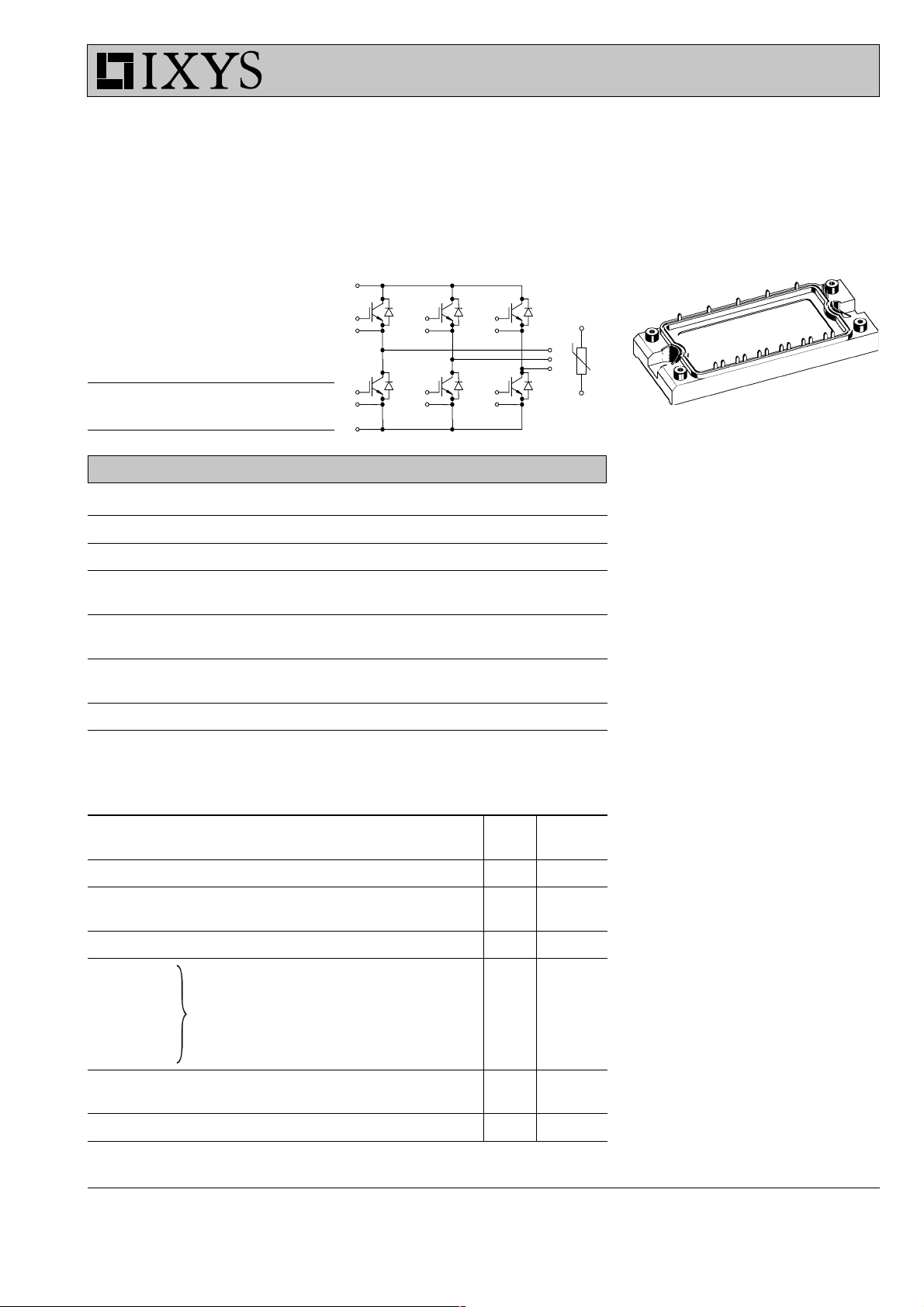
IGBT Modules
Sixpack
Short Circuit SOA Capability
Square RBSOA
13
Preliminary Data
Type: NTC - Option:
MWI 50-06 A7 without NTC
MWI 50-06 A7T with NTC
IGBTs
Symbol Conditions Maximum Ratings
V
CES
V
GES
I
C25
I
C80
RBSOA VGE = ±15 V; RG = 22 W; TVJ = 125°C I
t
SC
(SCSOA) non-repetitive
P
tot
Symbol Conditions Characteristic Values
V
CE(sat)
V
GE(th)
I
CES
TVJ = 25°C to 150°C 600 V
TC = 25°C 72 A
TC = 80°C 50 A
Clamped inductive load; L = 100 µH V
V
= V
CE
; VGE = ±15 V; RG = 22 W; TVJ = 125°C 10 µs
CES
TC = 25°C 225 W
IC = 50 A; VGE = 15 V; TVJ = 25°C 1.9 2.4 V
IC = 1 mA; VGE = V
V
= V
CE
CES; VGE
CE
= 0 V; TVJ = 25°C 0.6 mA
TVJ = 125°C 0.7 mA
1
2
3
4
17
(T
5
6
7
8
= 25°C, unless otherwise specified)
VJ
9
10
16
15
14
11
12
±
20 V
= 100 A
CM
£ V
CEK
CES
min. typ. max.
T
NTC
T
TVJ = 125°C 2.2 V
4.5 6.5 V
I
C25
V
CES
V
CE(sat) typ.
= 72 A
= 600 V
= 1.9 V
Features
●
NPT IGBT technology
●
low saturation voltage
●
low switching losses
●
switching frequency up to 30 kHz
●
square RBSOA, no latch up
●
high short circuit capability
●
positive temperature coefficient for
easy parallelling
●
MOS input, voltage controlled
●
ultra fast free wheeling diodes
●
solderable pins for PCB mounting
●
package with copper base plate
Advantages
●
space savings
●
reduced protection circuits
●
package designed for wave soldering
Typical Applications
●
AC motor control
●
AC servo and robot drives
●
power supplies
I
GES
t
d(on)
t
r
t
d(off)
t
f
E
E
C
Q
R
on
off
ies
Gon
thJC
VCE = 0 V; VGE = ± 20 V 200 nA
Inductive load, TVJ = 125°C
VCE = 300 V; IC = 50 A
VGE = ±15 V; RG = 22 W
VCE = 25 V; VGE = 0 V; f = 1 MHz 2800 pF
V
= 300V; VGE = 15 V; IC = 50 A 120 nC
CE
(per IGBT) 0.55 K/W
IXYS reserves the right to change limits, test conditions and dimensions.IXYS reserves the right to change limits, test conditions and dimensions.
© 2000 IXYS All rights reserved
50 ns
60 ns
300 ns
30 ns
2.3 mJ
1.7 mJ
023
1 - 4
Page 2
MWI 50-06 A7
MWI 50-06 A7T
Diodes
Symbol Conditions Maximum Ratings
I
F25
I
F80
TC = 25°C 72 A
TC = 80°C 45 A
Symbol Conditions Characteristic Values
min. typ. max.
V
F
I
RM
t
rr
R
thJC
IF = 50 A; VGE = 0 V; TVJ = 25°C 1.6 1.8 V
TVJ = 125°C 1.3 1.5 V
IF = 30 A; diF/dt = -500 A/µs; TVJ = 125°C 25 A
VR = 300 V; VGE = 0 V 90 ns
(per diode) 1.19 K/W
Temperature Sensor NTC (MWI ... A7T version only)
Symbol Conditions Characteristic Values
min. typ. max.
R
25
B
25/50
T = 25°C 4.75 5.0 5.25 kW
3375 K
Module
Symbol Conditions Maximum Ratings
T
VJ
T
stg
V
ISOL
M
d
I
£ 1 mA; 50/60 Hz 2500 V~
ISOL
Mounting torque (M5) 2.7 - 3.3 Nm
-40...+150 °C
-40...+125 °C
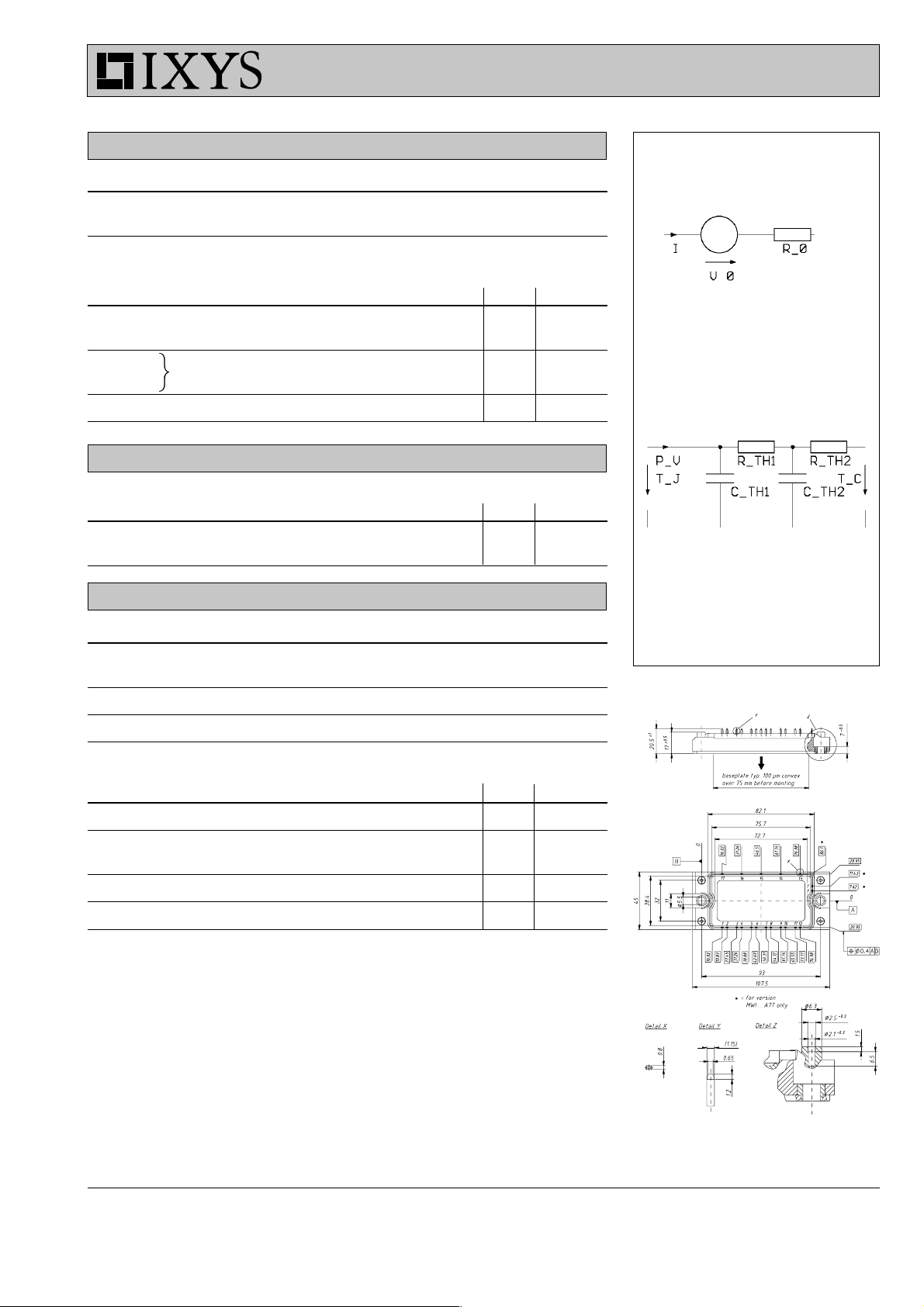
Equivalent Circuits for Simulation
Conduction
IGBT (typ. at VGE = 15 V; TJ = 125°C)
Free Wheeling Diode (typ. at TJ = 125°C)
Thermal Response
IGBT (typ.)
Free Wheeling Diode (typ.)
Dimensions in mm (1 mm = 0.0394")
V0 = 0.82 V; R0 = 28 mW
V0 = 0.89 V; R0 = 8 mW
C
= 0.201 J/K; R
th1
C
= 1.252 J/K; R
th2
C
= 0.116 J/K; R
th1
C
= 0.88 J/K; R
th2
= 0.42 K/W
th1
= 0.131K/W
th2
= 0.973 K/W
th1
= 0.217 K/W
th2
Symbol Conditions Characteristic Values
min. typ. max.
R
d
d
R
pin-chip
S
A
thCH
Creepage distance on surface 6 mm
Strike distance in air 6 mm
with heatsink compound 0.02 K/W
5mW
Weight 180 g
© 2000 IXYS All rights reserved
Higher magnification see outlines.pdf
2 - 4
Page 3

MWI 50-06 A7
MWI 50-06 A7T
150
A
120
I
C
VGE= 17V
15V
13V
90
60
30
TVJ = 25°C
0
0123456
V
CE
11V
9V
V
150
A
120
I
C
90
VGE= 17V
15V
13V
60
30
0
0123456
Fig. 1 Typ. output characteristics Fig. 2 Typ. output characteristics
150
A
120
I
C
90
60
= 125°C
T
VJ
TVJ = 25°C
30
0
4 6 8 10 12 14 16
V
GE
VCE = 20V
V
90
A
75
I
F
60
45
30
15
0
0.0 0.5 1.0 1.5 2.0
Fig. 3 Typ. transfer characteristics Fig. 4 Typ. forward characteristics of
free wheeling diode
V
V
CE
F
11V
9V
TVJ = 125°C
V
TVJ = 25°CTVJ = 125°C
V
20
V
15
V
GE
10
5
0
0 40 80 120 160
Fig. 5 Typ. turn on gate charge Fig. 6 Typ. turn off characteristics of
© 2000 IXYS All rights reserved
VCE = 300V
= 50A
I
C
Q
G
nC
50
40
A
t
I
RM
rr
30
20
10
I
RM
0
0 200 400 600 800 1000
-di/dt
free wheeling diode
TVJ = 125°C
V
= 300V
R
= 30A
I
F
MWI5006A7
A/ms
150
120
ns
90
60
30
0
3 - 4
t
rr
Page 4

MWI 50-06 A7
MWI 50-06 A7T
10.0
mJ
7.5
E
on
5.0
VCE = 300V
= ±15V
V
GE
R
= 22
2.5
E
on
0.0
04080120
G
TVJ = 125°C
I
C
A
t
t
d(on)
r
100
ns
75
t
50
W
25
0
4
mJ
3
E
off
2
1
0
0 40 80 120
V
= 300V
CE
= ±15V
V
GE
R
= 22
G
TVJ = 125°C
A
I
C
t
E
t
d(off)
f
400
ns
off
300
t
200
W
100
0
Fig. 7 Typ. turn on energy and switching Fig. 8 Typ. turn off energy and switching
times versus collector current times versus collector current
E
d(off)
600
ns
off
400
t
200
4
mJ
E
on
3
V
= 300V
CE
= ±15V
V
2
GE
I
= 50A
C
= 125°C
T
VJ
t
E
d(on)
on
t
r
80
ns
60
40
t
3
mJ
E
off
2
t
V
= 300V
CE
= ±15V
V
1
GE
= 50A
I
C
= 125°C
T
VJ
1
0 102030405060
R
G
Fig. 9 Typ. turn on energy and switching Fig.10 Typ. turn off energy and switching
times versus gate resistor times versus gate resistor
120
A
90
I
CM
60
30
RG = 22
W
= 125°C
T
VJ
0
0 100 200 300 400 500 600 700
Fig. 11 Reverse biased safe operating area Fig. 12 Typ. transient thermal impedance
RBSOA
t
f
20
W
0
0 102030405060
R
G
0
W
10
K/W
1
Z
thJC
diode
IGBT
0.1
0.01
0.001
0.0001
V
V
CE
0.00001 0.0001 0.001 0.01 0.1 1 10
single pulse
MWI5006A7
s
t
© 2000 IXYS All rights reserved
4 - 4
 Loading...