

Page 1
Features
Glass Passivated Die Construction
·
Super-Fast Recovery Time For High Efficiency
·
Low Forward Voltage Drop and High Current
·
Capability
Surge Overload Rating to 75A Peak
·
Ideally Suited for Automated Assembly
·
Plastic Material: UL Flammability
·
Classification Rating 94V-0
Mechanical Data
NEW PRODUCT
Case: Molded Plastic
·
Terminals: Solder Plated Terminal -
·
Solderable per MIL-STD-202, Method 208
Marking: U3D
·
Polarity: Cathode Band or Cathode Notch
·
Weight: 0.21 grams (approx.)
·
MURS320
3.0A SURFACE MOUNT SUPER-FAST RECTIFIER
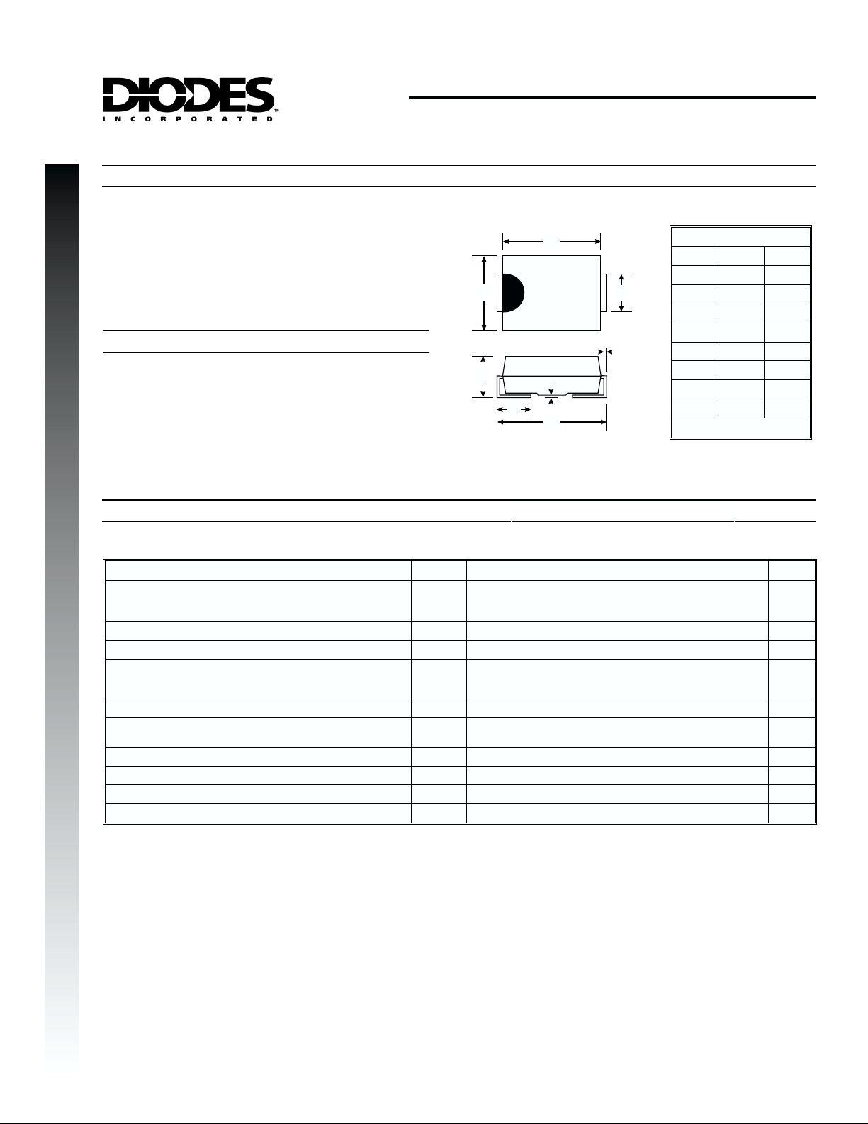
A
B
C
D
E
G
H
J
SMC
5.59 6.22
6.60 7.11
2.75 3.18
0.15 0.31
7.75 8.13
0.10 0.20
0.76 1.52
2.00 2.62
B
Dim Min Max
A
C
D
J
H
G
E
All Dimensions in mm
Maximum Ratings and Electrical Characteristics
Single phase, half wave, 60Hz, resistive or inductive load.
For capacitive load, derate current by 20%.
Characteristic Symbol MURS320 Unit
Peak Repetitive Reverse Voltage
Working Peak Reverse Voltage
DC Blocking Voltage
RMS Reverse Voltage
Average Rectified Output Current @ TL= 140°C
Non-Repetitive Peak Forward Surge Current
8.3ms Single half sine-wave Superimposed on Rated Load
(JEDEC Method)
Forward Voltage @ IF= 3.0A, TJ= 25°C
Peak Reverse Current @ TJ= 25°C
at Rated DC Blocking Voltage @ T
Reverse Recovery Time (Note 3)
Typical Junction Capacitance (Note 2)
Typical Thermal Resistance, Junction to Terminal (Note 1)
Operating and Storage Temperature Range
Notes: 1. Unit mounted on PC board with 5.0 mm2(0.013 mm thick) copper pads as heat sink.
2. Measured at 1.0MHz and applied reverse voltage of 0V DC.
3. Measured with I
= 0.5A, IR= 1.0A, Irr= 0.25A. See Figure 5.
F
= 150°C
J
V
V
V
, T
T
j
RRM
RWM
V
R
R(RMS)
I
O
I
FSM
V
FM
I
RM
t
rr
C
j
R
qJT
STG
@ TA= 25°C unless otherwise specified
200 V
140 V
3.0 A
75 A
0.9 V
5.0
100
25 ns
45 pF
11 K/W
-55 to +175 °C
mA
DS30197 Rev. A-0 1 of 2 MURS320
Page 2
g
100
g
4
10
T = 125ºC
j
3
2
NEW PRODUCT
1
O
I , AVERAGE FORWARD CURRENT (A)
0
25 50
75
50
75
100 125 150 175
T , TERMINAL TEMPERATURE ( C)
T
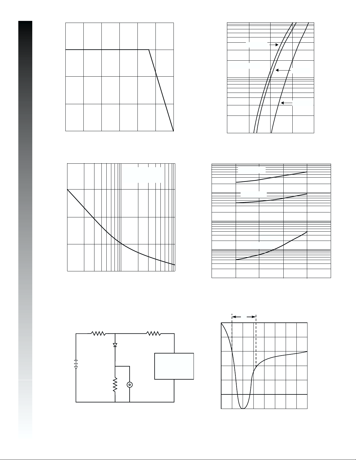
. 1 Forward Current DeratingCurve
Fi
Pulse width 8.3ms
Single Half-Sine-Wave
(JEDEC Method)
Pulse Width: 300us
0.5
F
I , INSTANTANEOUS FORWARD CURRENT (A)
0.1
0.2
°
0.4
V , INSTANTANEOUS VOLTAGE (V)
F
Fig.2 Typical Forward Current
0.6 0.8
T = 100ºC
j
T = 25ºC
j
1
100
T = 150ºC
j
10
T = 25ºC
j
1
25
FSM
I , PEAK FORWARD SURGE CURRENT (A)
0
1 10 100
NUMBER OF CYCLES AT 60Hz
. 3 Surge Current DeratingCurve
Fi
50 NI (Non-inductive)Ω
Device
Under
(+)
50V DC
Approx
(-)
Notes:
1. Rise Time = 7.0ns max. Input Impedance = 1.0M , 22pF.
2. Rise Time = 10ns max. Input Impedance = 50 .ΩΩ
Test
1.0NIΩ
Oscilloscope
(Note 1)
10 NIΩ
(-)
Pulse
Generator
(Note 2)
(+)
, REVERSE CURRENT (µA)
I
T = 25ºC
0.1
R
j
0.01
0
50 150
V , REVERSE VOLTAGE (V)
100
R
200
250
Fig. 4 Typical Reverse Current
t
+0.5A
0A
-0.25A
-1.0A
rr
Set time base for 50/100 ns/cm
Fig. 5 Reverse RecoveryTime Characteristic and Test Circuit
DS30197 Rev. A-0 2 of 2 MURS320
 Loading...