

Page 1
MUSIC Semiconductors Confidential 1 April 20, 2001 Rev 0.3 Draft
Advance Information
MUPA64K16 “Alto” Priority Queue Scheduler
General Description Features
The MUPA64K16 Alto Priority Queue Scheduler is a
high-performance sorting engine designed to support
packet scheduling in high-speed switch or router
applications. Alto can support any scheduling
algorithm for which a priority queue is required, such
as Weighted Fair Queuing, Start-Time Fair Queuing
and Self-Clocked Fair Queuing.
Alto holds 65,536 entries, each of which consists of a
32-bit sorting key and a 16-bit associated data value.
These 65,536 entries may be distributed evenly
across one, two, four, eight or sixteen independent
priority queues, where the number of elements
occupied in each of these queues is indicated by a
size register. Thus, Alto can support up to 65,536
FIFO queues distributed across up to 16 physical
switch ports.
Alto has a simple synchronous 32-bit interface as
well as a separate bus for expanding the associated
data field using external SRAM.
• Priority Queue with insert, extract and peek
operations
• Packet processing time of 150 ns
• 65,536 priority queue entries
• 32-bit sorting key
• 16-bit associated data value
• Supports up to 65,536 FIFO queues
• Supports up to 16 physical switch ports
• Wrap register per port handles counter roll-
over
• UID Manager generates unique associated
data values
• 32-bit synchronous data interface
• 17-bit SRAM address bus
• 15 ns clock
• 1.8V core / 3.3V I/O
• 128-pin LQFP package (14 x 20 mm)
• Industrial Temperature grade available
• IEEE 1149.1 JTAG boundary scan logic
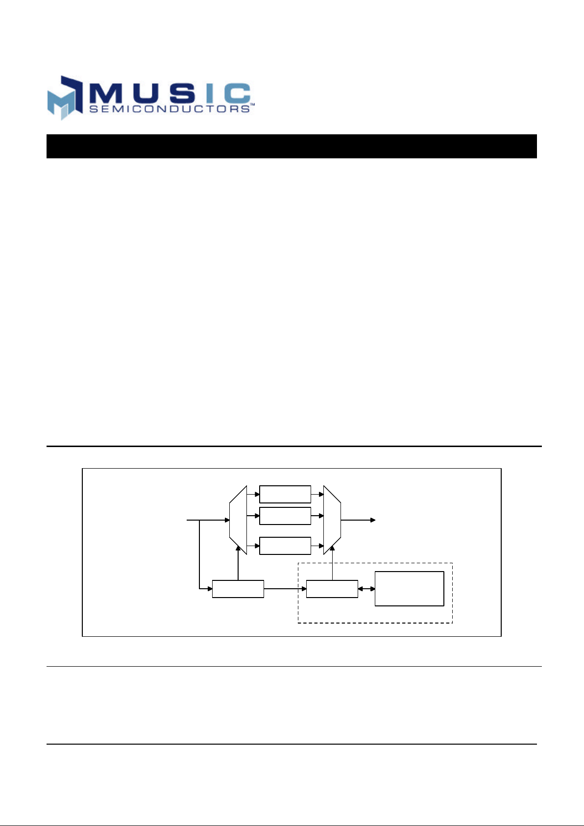
Packet Scheduler
Packet
Classifier
Packet Output
FIFO 1
FIFO 2
FIFO N
Control ASIC
MUSIC
Semiconductors
Alto
Packet Input
Figure 1: Packet Scheduling System Diagram
MUSIC Semiconductors, the MUSIC logo, and the phrase “MUSIC Semiconductors” are Registered Trademarks of MUSIC
Semiconductors. “MUSIC” is a trademark of MUSIC Semiconductors.
Page 2

MUPA64K16 Alto Priority Queue Scheduler
MUSIC Semiconductors Confidential 2 Rev 0.3 Draft
Table 1: Pin Description
Signal
Name
Function Function
REG[2.0] Input
Register Select. Selects the register to be read or written during a DQ[31:0] bus
operation.
OP[2:0] Input
Instruction Bus OP[2:0] selects the operation to be performed. See Table 5 showing op
codes for a list of legal values.
PQ[3.0] Input
Priority Queue Select. Selects the priority queue to which an operation applied. Note
that some operations, such as Noop, do not use this value.
/W Input
Read/Write. /W enables a register write or an operation that inputs data, such as Insert,
depending on the value of OP[2:0].
/CS Input
Chip Select. /CS indicates to the device that a new command is available on OP[2:0],
REG[2:0], PQ[3:0] and /W. If /W is zero, then /CS also indicates that there is new data
on the DQ[31:0]. /CS must be synchronous to CLK.
STR[4:0] Output
Status Register. Provides device status information; equivalent to bits 4:0 of the Status
Register (see Table 2).
CLK Input
Device clock. All internal operations and interface timings are synchronized to the rising
edge of the clock.
/RST Input
System Reset. The PLL in Alto requires 100 microseconds to stabilize after reset and
no commands should be issued during this time. Also, the UID manager requires an
additional 2200 clock cycles to initialize after this 100 microsecond interval.
AD[15:0] Output
Associated Data Bus. This bus outputs the associated data for interface to external
RAM. The contents of both the IDR and MDR are made available on this bus, selected
by ADS.
/ADV Output
Associated Data Bus Valid. ADV indicates the validity of the AD[15:0] bus. AD[15:0] is
invalid when ADS=1 and a peek or extract operation is performed on an empty priority
queue. /ADV signal is an address bit AD[16] of the Associated Data Bus, however,
AD[16] is not a part of the SRAM address.
ADS Input
Associated Data Bus Select. ADS determines whether the AD[15:0] bus carries the
value of the IDR (ADS=0) or the MDR (ADS=1).
/ADOE Input
Associated Data Bus Output Enable. /ADOE asynchronously enables Alto to drive the
AD[15:0] bus.
DQ[31:0] Input/Output
Data Bus. The bi-directional data bus writes to and reads from the registers. Data for
registers that are less than 32 bits occupy the least significant bits of DQ[31:0].
/DQOE Input
Data Bus Output Enable. Asynchronously enables the device to drive the DQ[31:0]
pins.
/RDY Input
READY. RDY indicates that the bus is idle and able to accept a new command.
/TRST Input JTAG reset pin.
TCLK Input JTAG Test Clock.
TMS Input JTAG Test Mode Select.
TDI Input JTAG Test data Input.
TDO Output JTAG Test Data Output.
V
DD
Power Supply Voltage for Core (1.8V)
V
DDQ
Power Supply Voltage for I/O (3.3V)
V
SS
GND Ground
AV
DD
Input Supply Voltage for PLL (1.8V)
AV
SS
GND Ground for PLL
Page 3
MUPA64K16 Alto Priority Queue Scheduler
MUSIC Semiconductors Confidential 3 Rev 0.3 Draft
Functional Description
This section provides an overview of the use of the
Alto device. Detailed information is provided
elsewhere in this document.
The Alto priority queue is a high-performance sorting
engine designed to support packet scheduling in
Ethernet and ATM switches. Alto supports packet
scheduling for up to 16 physical queues, with a total of
up to 65,536 per flow or per virtual circuit queues.
The Alto device also contains a Unique Identifier
(UID) manager that provides an associated data value
that is not in use for a specific queue. The UID
generator is independent of the priority queue and its
use is optional. The UID generator can be used to
assist with queuing memory management by selecting
an unused packet storage location. The priority queue
functionality and the UID manager functionality are
independent of each other, so either can be used
without the other, or both can be used together.
Alto provides a simple synchronous interface that
consists of a 32-bit bi-directional data bus (DQ[31:0]),
a register selection input (REG[2:0]), a read/write
input (/W), and a priority queue selection input
(PQ[3:0]). In addition, device status can be read from
a register over the DQ[31:0] bus or obtained directly
from the STR[4:0] pins. Alto also provides a separate
address output bus (AD[15:0]) that can be used to
drive an external SRAM, if desired.
The Alto device stores <key, data> pairs in a priority
queue such that the entry with the minimum key value
is at the top of the queue. The basic operations of the
device allow new entries to be inserted into the priority
queue or the entry with the minimum key value to be
extracted from the priority queue. Other operations
include the ability to read the entry with the minimum
key value without altering the priority queue, or to
perform both an extraction and an insertion
simultaneously. Figure 3 shows datapath for the
device registers.
The Alto device holds 64K entries, each of which
consists of a 32-bit key and 16 bits of associated data.
The 65,536 entries can be distributed evenly among
one, two, four, eight or sixteen priority queues. A Size
Register for each priority queue indicates the number
of elements in the queues. If the key values are based
on time, or any other monotonically increasing value,
there will come a time at which the 32-bit key value
will wrap. The Alto device includes a Wrap Register,
which indicates the key value that is to be treated as
the minimum value. For example, if the Wrap Register
is set to one, then one will be treated as the minimum
key value, two will be the next value and zero will be
considered the maximum key value. Each priority
queue has its own Wrap Register.
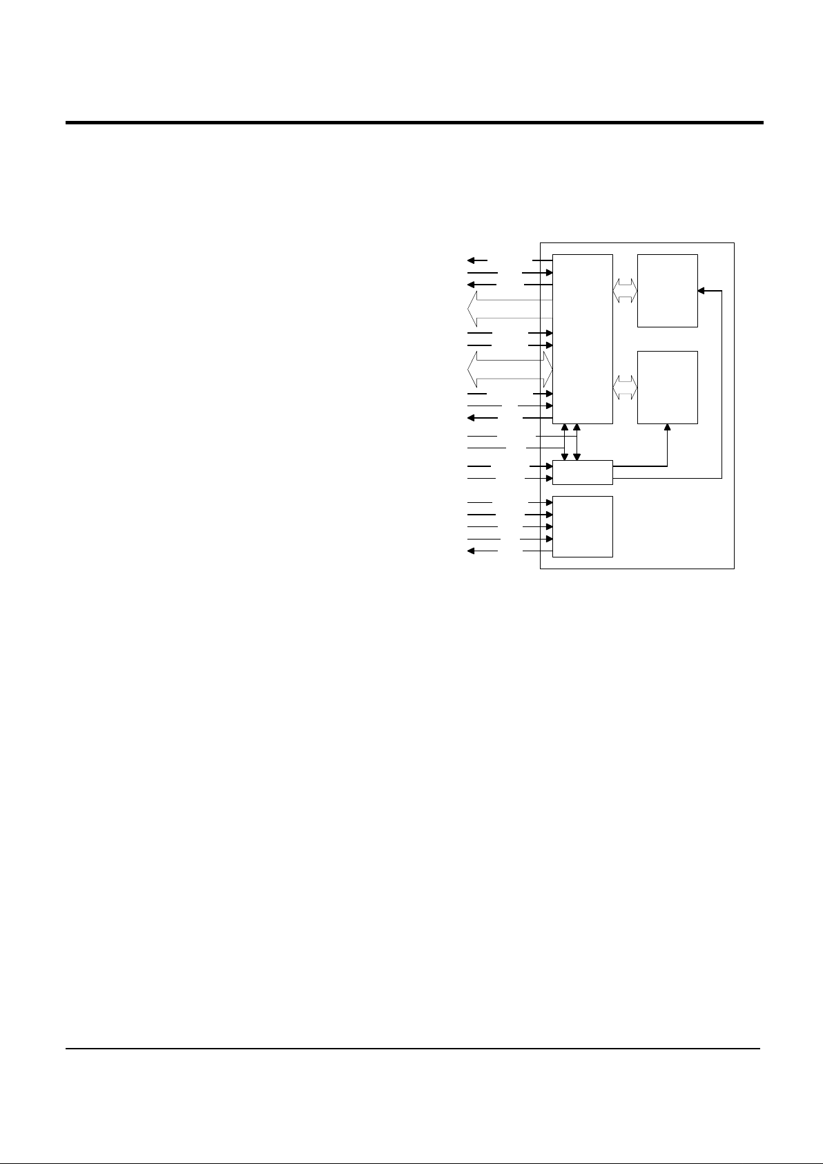
The functional block diagram of the MUPA64K16 is
shown in Figure 2. The device contains a set of
registers, a priority queue and a Unique Identifier
Manager.
DQ[31:0]
Priority
Queue
Registers
OP[2:0]
PQ[3:0]
/DQOE
JTAG
TRSTb
TCLK
TMS
TDI
TDO
AD[15:0]
/ADOE
STR[4:0]
REG[2:0]
/W
RSTb
ADS
RDY
Operand
Decoder
/CS
UID
Manager
/ADV
Figure 2: Functional block diagram.
Priority Queue
The priority queue logic block implements a priority
queue that contains 65,536 <key, data> pair
combinations. The key is a 32-bit value that is sorted
by the priority queue and the data is a 16-bit data field
that can contain an arbitrary value. This block
contains the instruction logic for all the queue
operations.
The basic operations of the priority queue are:
• INSERT a new <key, data> pair
• EXTRACT returns the minimum <key, data> pair
as selected by the PQ[3:0] inputs
• BOTH performs Extract and Insert both
operations
• PEEK returns the minimum <key, data> pair as
selected by the PQ[3:0] inputs
Priority Queue logic block receives instructions and
related data from the registers and generates the
output data and the control signals to update the
Status Register. The execution of the instruction is
indicated by the “DONE” signal, which is sent to the
registers to prepare for the next instruction from the
registers.
Unique Identifier (UID) Manager
The UID Manager stores up to 64K 16-bit unused
data elements, each of which represents a unique
Page 4

MUPA64K16 Alto Priority Queue Scheduler
MUSIC Semiconductors Confidential 4 Rev 0.3 Draft
identifier. The UID Manager returns the lowest unused
identifier, and replaces any identifier currently not
used. The basic operations of the UID manager are:
• UID Get: obtain an unused UID
• UID Put: return a UID to the pool of unused UIDs
Pipeline operations are supported; as soon as an
operation begins execution, the input registers are
available to receive data for the next operation.
The contents of the Size Register (SR) are cleared
when either the Mode Register (MR) or the Size
Register (SR) detects a WRITE operation. When the
priority queue (PQ) line addresses the SR, the
contents of the SR will be incremented or
decremented by one for INSERT or EXTRACT
operations. The respective Wrap Register (WR) will
be updated via the DQ input port using the PQ line
value and the contents of the Mode Register (MR).
Similarly, the contents of the WR will be cleared when
the MR detects the WRITE operation.
The contents of the Size Registers (SR), Wrap
Registers(WR), Input Key Register (IKR), Input Data
Register(IDR), priority queue, and opcode are stored
in the packet buffer when any of these instructions
(INSERT, EXTRACT, BOTH, PEEK) are detected.
After the completion of the previously issued queue
instruction, these contents are transferred to the
priority queue to execute the priority queue’s next
instruction.
The input buffers are now available to accept
additional queue instructions from the external I/O
interface. Any additional new instructions can be
issued after checking the status information (STR) bits
(either 0 or 1 depending upon the instruction).
STR[4:0] (Status, Output)
STR[4:0] provide device status information, and is
equivalent to Status Register bits 4:0.
• STR[0] is one if IKR and IDR are ready to accept
new values; STR[0] is zero if a command has
been issued, but execution has not yet started.
• STR[1] is one if MKR and MDR contain new
values to be read; STR[1] is reset to zero if either
the MKR or MDR registers are read.
• STR[2] is one if the UPR is ready to accept a new
value.
• STR[3] is one off any UGR contains a new UID
value to be read.
• STR[4] is one if the most recent UID Get
operation completed and the associated UID Get
Register contains the new UID value.
Register Descriptions
Table 2 gives an overview of the device registers and
their attributes. Figure 3 shows the register datapath.
Input Data Register (1 x 16 bits)
The Input Data Register (IDR) is loaded with an
associated data value for the next INSERT or BOTH
instruction. The IDR is write only. The IDR can be
read via the AD[15:0] bus when ADS is zero.
Input Key Register (1 x 32 bits)
The Input Key Register (IKR) is loaded with an key
value for the next INSERT or BOTH instruction. The
IKR is write only.
Min Data Register (1 x 16 bits)
The Min Data Register (MDR) contains the data
associated with the minimum key of the selected
priority queue. The MDR is loaded by Peek, Extract
and Both instructions. The MDR is read only. The
MDR can be read via the AD[15:0] bus when ADS is
one.
Min Key Register (1 x 32 bits)
The Min Key Register (MKR) contains the minimum
key of the selected priority queue. The MKR is loaded
by the Peek, Extract and Both instructions. The MKR
is read only.
Mode Register (1 x 3 bits)
The Mode Register (MR) bits select the number of
priority queues:
• 0: one priority queue (64K each)
• 1: two priority queues (32K each)
• 2: four priority queues (16K each)
• 3: eight priority queues (8K each)
• 4, 5, 6, 7: sixteen priority queues (4K each)
The MR is read/write and is initialized to all zeros.
Table 3 shows how the MR value affects other
registers in the device.
Note: Writing to the mode register will reset all Size
Registers and all Wrap Registers to zero.
Page 5
MUPA64K16 Alto Priority Queue Scheduler
MUSIC Semiconductors Confidential 5 Rev 0.3 Draft
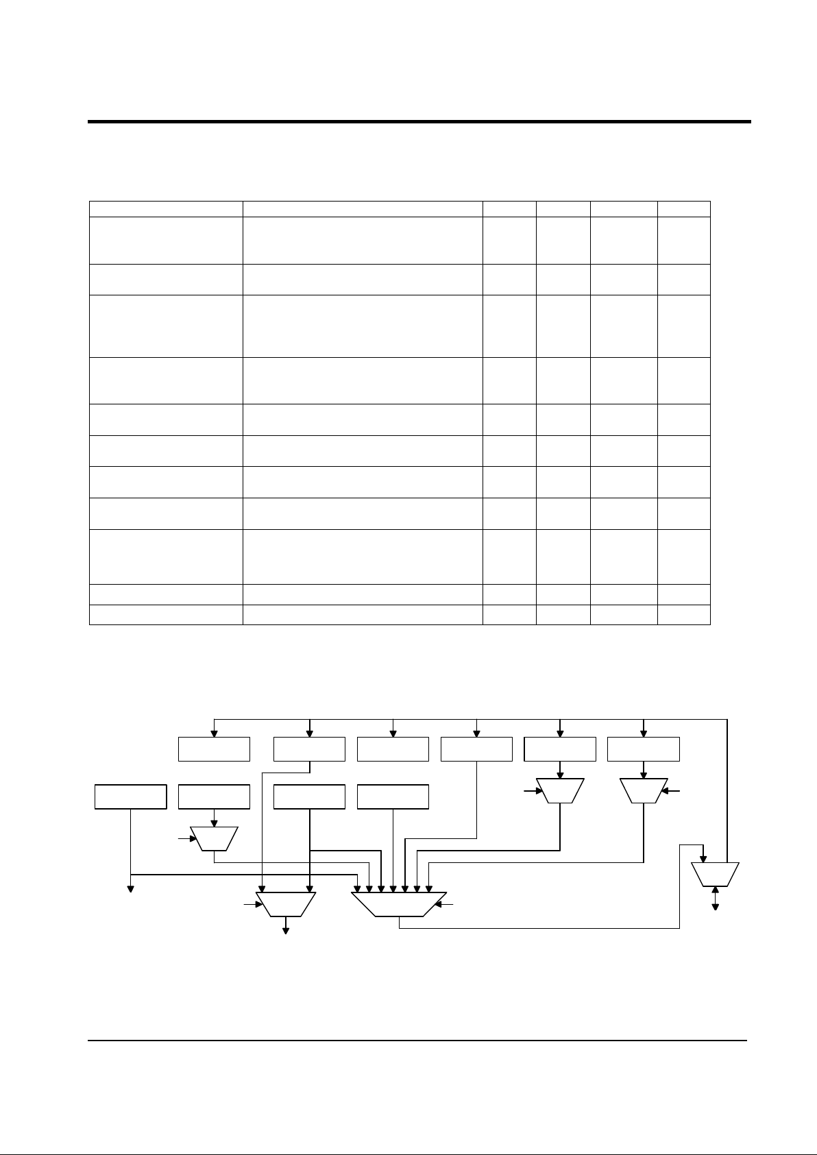
Table 2: Registers
Register Description R/W Size Reg[2:0] /W
Input Data Register
(IDR)
Contains the associated data value
for the next INSERT or BOTH
instruction
W 16 1 0
Input Key Register
(IKR)
Contains the key value for the next
INSERT or BOTH instruction W 32 0 0
Minimum Data
Register
(MDR)
Contains the data associated with the
minimum key value returned by a
PEEK, EXTRACT or BOTH
instruction
R 16 1 1
Minimum Key Register
(MKR)
Contains the minimum key value
returned by the PEEK, EXTRACT or
BOTH instruction
R 32 0 1
Size Registers (16)
(SR)
Indicates the size of each of the
priority queues R/W 17 2 0/1
Wrap Registers (16)
(WR)
Holds the value that is to be
considered minimum R/W 32 3 0/1
UID Get Registers (16)
(UGR)
Holds the next available unique
identifier that is not in use R 17 5 1
UID Put Register
(UPR)
Accepts identifiers that are no longer
in use to be returned to the free list W 16 5 0
Mode Register (MR) Determines the number of
independent priority queues in use: 1,
2 4, 8 or 16
R/W 3 4 0/1
Status Register (STR) Provides device status R 21 6 1
Reserved R/W N/A 7 0/1
ADS
PQ[3:0]
PQ[3:0] PQ[3:0]
MUX
MUX
UID Put
Register
Size
Register x16
Status
Register
Input Data
Register
Input Key
Register
MUX
DQ[31:0]
REG[2:0]
Wrap
Register x16
Mode
Register
Min Data
Register
Min Key
Register
UID Get
Register x16
MUX MUX
STR[4:0] MUX
AD[15:0]
Figure 3: Register Datapath
Page 6
MUPA64K16 Alto Priority Queue Scheduler
MUSIC Semiconductors Confidential 6 Rev 0.3 Draft
Table 3: Relationship Among Registers
MR[2:0]
Number
Of
Queues
PQ
Lines
Used
Number of
UID Get
Registers
Number
Of Wrap
Registers
Number
Of Size
Registers
Width of
Size
Register
000 1 none
1
1 1 17 bits
001 2 PQ[0]
2
2 2 16 bits
010 4 PQ[1:0]
4
4 4 15 bits
011 8 PQ[2:0]
8
8 8 14 bits
100, 101 16 PQ[3:0]
16
16 16 13 bits
110, 111
As seen in Table 3, although the Size Register, Wrap
Register and UID Get Register are replicated 16
times, not all of these registers are accessible if the
MR value is less than four.
Table 4: Status Register
Bit 0 If Bit 0 is ‘1’ IKR and IDR are ready to
accept new values; If Bit 0 is ‘0’ if a
command has been issued, but execution
has not yet started.
Bit 1 If Bit 1 is ‘1’ MKR and MDR contain new
values to be read; If Bit 1 is reset to zero,
either the MKR or MDR registers are
read.
Bit 2 If Bit 2 is ‘1” the UPR is ready to accept a
new UID value.
Bit 3 If Bit 3 is ‘1’ any UGR contains a new UID
value to be read.
Bit 4 If Bit 4 is ‘1’ the most recent UID Get
operation completed and the associated
UID Get Register contains the new UID
value.
Bit
[20:5]
Bits [20:5] provide the status of the most
recent UID Get operation for each
individual UID Get Register. Bit 5 is ‘1’ if
the most recent UID Get operation
completed for queue zero, Bit 6 is ‘1’ if the
most recent UID Get operation completed
for queue one, and so forth.
The STR is read only. Bits 4:0 of the Status Register
can be read directly on pins STR[4:0].
Size Register (16 x 17 bits)
The Size Register (SR) contains the number of active
entries in the priority queue as selected by PQ[3:0].
Note that each SR ranges from zero to N, where N is
the maximum number of elements in the queue. Each
priority queues has its own SR. The size can be read
and a write to the SR sets the priority queue size to
zero. The SR is read only. A write to the SR will reset
its value to zero after the current operation
completes. All SRs are initialized to zero.
Wrap Register (16 x 32 bits)
The Wrap Register (WR) contains the minimum key
value for the priority queue as selected by PQ[3:0]. If
the WR contains the value N, then N is considered to
be the smallest key value and N-1 is considered to be
the largest key value. Each priority queues has its
own WR. The WR is read/write, although the new
wrap value will not be used until after the current
operation completes. All WRs are initialized to zero.
UID Get Register (16 x 17 bits)
Each UID Get Register (UGR) contains an identifier
for the priority queue as selected by PQ[3:0]. A
separate UGR exists for each priority queue to allow
these identifiers to be generated in advance. The
minimum UID is zero and the maximum UID is one
less than the maximum number of elements for a
queue. The identifiers are unique only within a queue
and not among queues. Bits 15:0 contain the UID
value. Bit 16 indicates whether bits 15:0 are valid. Bit
17 indicates whether the UGR has a new value since
the last time that it was read. The UGRs are read
only registers.
UID Put Register (1 x 16 bits)
The UID Put Register (UPR) accepts identifiers that
are no longer in use so that they can be reused. The
unique identifier is returned to the free list of UIDs for
the priority queue selected by PQ[3:0]. The UPR is
write only register.
Page 7

MUPA64K16 Alto Priority Queue Scheduler
MUSIC Semiconductors Confidential 7 Rev 0.3 Draft
Operational Description
All instructions either accept new data from registers
or return data to registers. All I/O operations read and
write registers. An input operation (e.g., Insert) is
performed by writing data to registers, then triggering
the operation; an output operation (e.g., Extract) is
performed by triggering the operation, then reading
data from registers.
Each operation described below requires a fixed
number of clock cycles to perform. The operations
are broken into three classes: register operations,
priority queue operations, and UID operations. Within
a class, only one operation can be run at a time.
However, operations in different classes can run in
parallel.
The ability to run several operations in parallel means
Insert, Extract and Both operations can be pipelined
such that a result is obtained every nine clock cycles.
Operation results can be read from registers and new
information written to registers while the priority
queue operation is in progress. The device will idle
and perform no operation if an operation completes
and no new operation has been chosen.
Every operation across the DQ[31:0] bus accesses a
register for read or write. In addition, the register
operation can be combined with the command to
start a priority queue operation. Consider inserting a
<key, data> pair using two register writes. The first
command is a register write to the IDR. The second
command is an Insert with the IKR selected. This has
the effect of writing the IKR and at the same time,
commanding the device to start a priority queue
Insert operation as soon as any previous operation
has completed. To start an operation without
modifying a register, simply perform a register read
rather than a register write.
Table 5 shows a list of the operations and the op
code necessary to invoke them. Note that the
complete op code is provided by the combination of
OP[2:0], /W, PQ[3:0] and REG[2:0]. So for the
example above of writing the IKR while starting an
Insert operation for queue 5, OP[2:0] = 1, /W = 0,
PQ[3:0] = 5, REG[2:0] = 0
Table 5: Op codes and the registers used
Instruction OP[2:0] Inputs Outputs
Noop 0 None None
Insert 1 IDR, IKR,
PQ[3:0]
AD[15:0]
Extract 2 PQ[3:0] MDR, MKR,
AD[15:0]
Both 3 IDR, IKR,
PQ[3:0]
MDR, MKR,
AD[15:0]
Peek 4 PQ[3:0] MDR, MKR,
AD[15:0]
UID Get 5 PQ[3:0] UGR
UID Put 6 UPR,
PQ[3:0]
None
RESERVED 7 N/A N/A
REGISTER OPERATIONS
Register Read/Write
A Register Read/Write accesses a register for read or
write, but that no priority queue operation is selected.
Register Read/Write may occur in parallel with other
operations.
Alto registers can be read and written using the
synchronous interface that consists of a 32-bit bidirectional data bus (DQ[31:0]), a register select input
(REG[2:0]), a read/write input (/W), and a priority
queue selection input (PQ[3:0]). The Status Register
also can be read from pins STR[4:0]. The Input Data
Register and the Min Data Register can be read with
the address output bus (AD[15:0]) for interface to
external SRAM.
The device allows pipelined operations; separate
registers are provided for data input and data output.
Data can be written to and read from registers while
the priority queue controller or the UID manager
controller are performing operations.
A register operation can be combined with a
command to start either a priority queue operation or
a UID manager operation. Consider inserting a <key,
data> pair into the priority queue using two register
write operations. The first register operation writes
the Input Key Register. The second register operation
writes the Input Data Register and simultaneously
requests the start of an Input operation to the priority
queue. If it is desirable to start a priority queue
operation or a UID manager operation without
modifying a register, the request to start an operation
can be combined with a register write operation.
Page 8

MUPA64K16 Alto Priority Queue Scheduler
MUSIC Semiconductors Confidential 8 Rev 0.3 Draft
PRIORITY QUEUE OPERATIONS
Alto stores <key, data> pairs in a priority queue such
that the entry with the minimum key value is at the
top of the queue. The basic operations of Alto allow
new entries to be inserted into the priority queue or
the entry with the minimum key value to be extracted
from the priority queue. Additional operations include
the reading of minimum key values without altering
the priority queue and a single operation that
combines an insert and an extract operation. If a
priority queue operation completes, the priority queue
controller will go idle until the next operation is
triggered.
Insert
The INSERT operation takes a key from the Input
Key Register and associated data from the Input
Data Register and inputs a new key/associated data
pair into the priority queue selected by PQ[3:0]. The
associated data written with the key is made
available in the Min Data Register and, if ADS is
zero, on the AD[15:0] bus. INSERT requires ten clock
cycles.
Peek
The PEEK operation returns the minimum key and its
associated data in the priority queue as selected by
PQ[3:0], but it does not change the priority queue
itself. PEEK returns the minimum key via the Min Key
Register and the associated data in the Min Data
Register and, if ADS is zero, on the AD[15:0] bus.
PEEK requires three clock cycles.
Extract
The EXTRACT operation returns the minimum key
and its associated data in the priority queue as
selected by PQ[3:0] and removes the element from
the priority queue. EXTRACT returns the minimum
key via the Min Key Register and the associated data
in the Min Data Register and, if ADS is zero, on the
AD[15:0] bus. EXTRACT requires ten clock cycles.
Both
The BOTH operation performs an EXTRACT and an
INSERT in a single operation. The BOTH operation
requires ten clock cycles.
If BOTH is performed on an empty priority queue, the
returned value is the same as the inserted value and
the priority queue remains empty.
If BOTH is performed on a full priority queue, the
inserted value is returned if its key is less than or
equal to the minimum key in the priority queue.
Otherwise, the entry with the minimum key is
returned from the priority queue and the new value is
inserted. In either case, the priority queue remains
full.
Whenever possible the designer should utilize the
BOTH operation, since this operation will be
completed within 150ns, rather than separate
INSERT and EXTRACT operations (a duration of
300ns), to maximize the device performance.
UNIQUE IDENTIFIER (UID) OPERATIONS
Alto also contains a Unique Identifier (UID) Manager.
This provides an associated data value which is not
in use for specific queues and is used to maintain a
list of unused packet buffers. The UID Manager can
generate independent priority queues and assist with
the queue memory management by selecting unused
packet storage locations. Both the priority queue and
UID Manager can function independently of each
other; so either one can be used without the other, or
both can be used together.
UID Get
The UID Get operation selects an unused identifier
for the priority queue selected by PQ[3:0] and makes
it available in the UID Get Register. The UID Get
operation requires nine clock cycles.
UID Put
The UID Put operation retrieves a UID value from the
UID Put Register and returns it to the list of unused
identifiers for the priority queue selected by PQ[3:0].
The UID Put operation requires three clock cycles.
RESET OPERATION
Power-Up Reset
Note that core voltage is 1.8V and this determines
when the PLL initializes.
When VDD is initially applied to Alto it will take some
amount of time for power to actually reach the
nominal 1.8V potential. Generally, this initial powerup time is called, “VDD ramp” when VDD is, “ramping”
from 0V to 1.8V. When the initial ramp reaches
approximately 80%, or 1.44V, Alto begins an internal
reset operation which must be allowed sufficient time,
relative to the assertion and deassertion of the
RESET pin, to reset Alto. There are two methods to
guarantee reset upon device power-up.
The first method accounts for those applications that
utilize a special power-up circuit which, through
hardware, will assert the reset pin upon power-up. In
this case, the deassertion (fall edge) of the RESET
pin must not occur until at least 100µs after the time
at which VDD ramp initially reached the 1.8V
threshold.
The second method accounts for those applications
which produce a reset pulse some time after the
initial power-up sequence. In this case, it is
recommended that a positive pulse, with a duration of
at least 100µs, be applied to the RESET pin no
sooner than 100µs after the point in time where the
initial VDD has reached 1.8V.
Page 9

MUPA64K16 Alto Priority Queue Scheduler
MUSIC Semiconductors Confidential 9 Rev 0.3 Draft
In both methods described, it is important to note that
the logic levels present at each of the hardware
configuration pins are also latched into Alto as a
function of the reset operation (hardware or
software). These hardware configuration values are
guaranteed to be latched into Alto 100µs after the
deassertion of the RESET pin.
The hardware configuration values latched into the
during the reset operation are dependent upon the
logic levels present at Alto pins, upon power-up. The
66MHz clock reference must be applied for reset to
take effect.
Hardware Reset
The hardware reset operation requires that the reset
pin (/RST) be asserted for a minimum of three
continuous clock cycles during normal operation.
When the hardware reset operation occurs as the
part of power-up sequence; the PLL requires a lock
time of 100 µs based on external clock. Only after the
PLL has locked the frequency will the instructions be
recognized.
The PLL in Alto requires 100µs to stabilize after reset
and no commands should be issued during this time.
Also, the UID manager requires an additional 2200
clock cycles to initialize after this 100µs interval.
The MDR, MKR, MR, SRs, UGR and WRs all are
reset to zero. The STR (Status Register) should
become 0001. After 2200 clock cycles to initialize the
UID system, the STR should become 0101.
Software Reset
The software reset operation can be accomplished by
writing into the Mode Register. This will cause a
software reset of the device, even if Alto has recently
completed a hardware reset. When more than one
priority queue is desired, the Mode Register must first
be set to the appropriate value. The software reset
takes approximately 100µs. Both the hardware reset
and software reset will reset Alto such that all
registers and state machines will be reset to default
values and the hardware configuration values will be
re-latched into Alto (similar to power-up/reset
operation). Driver code should wait 100µs following a
software reset before interfacing with the device.
Since the internal device requires 2200 clock cycles
(a duration of 33 µs) to initialize; no instructions
should be issued within this time period.
INSTRUCTION SEQUENCES
The basic operation of Alto is simple. For input
operations, data is written to registers and the
operation is started. For output operation, the
operation is started and the results are read from
registers when the operation is complete. Figure 4
shows the normal data flow through Alto.
The way to perform each basic operation is shown
below. Operation completion can be determined
using the Status Register, using the status pins
(STR[4:0]) or by counting clock cycles.
The Insert, Extract, Both, and Peek operations are
performed as shown in Tables 6, 7, 8, and 9. A UID
Get operation is performed as shown in Table 10,
and a UID Put operation is performed as shown in
Table 11.
Operations can be pipelined and interleaved; also,
priority queue operations and UID manager
operations can execute in parallel. When an
operation is started, the values of the appropriate
registers are loaded into the execution unit. The input
registers are available to hold new input values. If a
new operation is requested of an execution unit that
is busy, the new operation will begin as soon as the
previous operation is complete. The instruction FIFO
for each execution unit is one deep; issuing two or
more new instructions to an execution unit that is
busy will cause only one of the instructions to
execute.
Status
Register
Mode
Register
Priority Queue
Wrap
Register x16
Size Register
x16
Input Data
Register
Input Key
Register
Min Data
Register
Min Key
Register
UID Manager
UID Put
Register
UID Get
Register x16
Figure 4: Dataflow diagram
Page 10

MUPA64K16 Alto Priority Queue Scheduler
MUSIC Semiconductors Confidential 10 Rev 0.3 Draft
Table 6: Insert Operation
Operation Instruction OP[2:0] REG[2:0] /W PQ[3:0]
Write IKR Noop 0 0 0 N/A
Write IDR,
start Insert
Insert 1 1 0 N
Table 7: Extract Operation
Operation Instruction OP[2:0] REG[2:0] /W PQ[3:0]
Start Extract Extract 2 N/A 1 N
Wait for
Extract to
complete
Read MDR Noop 0 1 1 N/A
Read MKR
(if desired)
Noop 0 0 1 N/A
Table 8: Peek Operation
Operation Instruction OP[2:0] REG[2:0] /W PQ[3:0]
Start Peek Peek 4 N/A 1 N
Wait for
Peek to
complete
Read MDR Noop 0 1 1 N/A
Read MKR
(if desired)
Noop 0 0 1 N/A
Table 9: Both Operation
Operation Instruction OP[2:0] REG[2:0] /W PQ[3:0]
Write IKR Noop 0 0 0 N/A
Write IDR,
start Both
Both 3 1 0 N
Wait for Both
to complete
Read MDR Noop 0 1 1 N/A
Read MKR
(if desired)
Noop 0 0 1 N/A
Page 11

MUPA64K16 Alto Priority Queue Scheduler
MUSIC Semiconductors Confidential 11 Rev 0.3 Draft
Table 10: UID Get Operation
Operation Instruction OP[2:0] REG[2:0] /W PQ[3:0]
Start UID
Get
UID Get 5 N/A 1 N
Wait for UID
Get to
complete
Read UGR Noop 0 5 1 N
Table 11: UID Put Operation
Operation Instruction OP[2:0] REG[2:0] /W PQ[3:0]
Write UPR,
Start UID
Put
UID Put 6 6 0 N
Table 12: Size and Wrap Registers
MR[2:0] Number of
Queues
Number of
Size
Registers
Number of
Wrap registers
Width of
Size register
PQ Lines
used
000 1 1 1 16 bits none
001 2 2 2 15 bits PQ[0]
010 4 4 4 14 bits PQ[1,0]
011 8 8 8 13 bits PQ[2:0]
100, 101,
110, 111
16 16 16 12 bits PQ[3:0]
Size and Wrap register bank and instruction
decode
The SWM module contains: Instruction decode and
write logic for 16 SR (Size) registers and 16 WR
(Wrap) registers. Priority queue can be configured
with use of PQ[3:0] inputs and mode register bits
MR[2:0]. Table 12 shows the relationship between
the PQ[3:0], MR[2:0] and number of queues.
Decode logic for queue operation instructions: insert,
extract, both, peek, Ram Write, Ram Read. Decode
logic for instruction that reads size and wrap register
contents pointed to by PQ inputs.
Size register contents are cleared when a write is
detected either for mode register or for size register.
Size register contents pointed to by PQ and mode
register are increased or decreased by one if an
instruction in execution is insert or extract.
Wrap register contents are cleared when a write is
detected for mode register. When a write is detected
for wrap register, using PQ value and mode register
contents, appropriate wrap register is updated from
DQ input.
When an instruction that operates on queue (insert,
extract, peek, both) is detected, PQ, opcode, size
register, wrap register, IKR and IDR are stored in a
buffer. Upon detection of completion of previously
issued queue instruction, the contents are
transferred to the priority queue for execution of the
queue instruction. The buffer is now ready to accept
one additional queue instruction from external
interface.
If it is not required to read the Size Register all the
time, it can be tracked in ASIC.
The following is an example of a complex set of
pipelined instructions. The basic sequence is six
instructions, but they're interleaved to achieve
optimal pipelining.
Page 12

MUPA64K16 Alto Priority Queue Scheduler
MUSIC Semiconductors Confidential 12 Rev 0.3 Draft
Table 13: Pipeline Instructions
Pipeline
Cycle
Clock
Cycle
Operation Instruction OP[2:0] REG[2:0] /W PQ[3:0]
P 1 Read UGR, Start UID Get (9
clocks)
UID Get 5 5 1 N
P-1 4 Wait for Both to complete
P-1 7 Read MDR Noop 0 1 1 N/A
P-1 10 Read MKR (if desired) Noop 0 0 1 N/A
P 13 Write IKR Noop 0 0 0 N/A
P 15 Write IDR, start Both (10 clocks) Both 3 1 0 N
P-1 17 Write UPR, Start UID Put (3
clocks
UID Put 6 6 0 N/A
P+1 19 Read UGR, Start UID Get UID Get 5 5 1 N
P 22 Wait for Both to complete
P 25 Read MDR Noop 0 1 1 N/A
P 28 Read MKR (if desired) Noop 0 0 1 N/A
P+1 31 Write IKR Noop 0 0 0 N/A
P+1 33 Write IDR, start Both (10 clocks) Both 3 1 0 N
P 35 Write UPR, Start UID Put UID Put 6 6 0 N/A
JTAG INTERFACE
This section contains the Test Access Port and
Boundary Scan Architecture as specified by the IEEE
JTAG standard 1149.1. It consists of five JTAG
interface signals TCK, TMS, /TRST, TDI and TDO.
/TRST (JTAG Reset, Input)
/TRST is the Test Reset input.
TCLK (JTAG Test Clock, Input)
TCLK is the Test Clock input.
TMS (JTAG Test Mode Select, Input)
TMS is the Test Mode Select input.
TDI (JTAG Test Data Input, Input)
TDI is the Test Data input.
TDO (JTAG Test Data Output, Output)
TDO is the Test Data output.
Page 13

MUPA64K16 Alto Priority Queue Scheduler
MUSIC Semiconductors Confidential 13 Rev 0.3 Draft
Timing Diagrams
Bus Interface Unit Timing Diagram (Synchronous)
The BIU interface timing diagrams for various input cycles are shown below.
Figure 5: Single Command Operation
thdpq
tsupq
thdreg
tsureg
thdcs
tsucs
NOOP NOOP
Command
CLK
/CS
REG[2:0]
PQ[3:0]
Figure 6: Single Read Operation
Page 14

MUPA64K16 Alto Priority Queue Scheduler
MUSIC Semiconductors Confidential 14 Rev 0.3 Draft
Figure 7: Single Write Operation
Figure 8: Read Followed by Read Operation
Page 15

MUPA64K16 Alto Priority Queue Scheduler
MUSIC Semiconductors Confidential 15 Rev 0.3 Draft
Figure 9: Read Followed by Write Operation
Figure 10: Write Followed by Read Operation
tdout
thddq
tsudq
thdpqthdpq
tsupq
thdreg
thdreg_sel
tsureg
thdwr
tsuwr
thdcs
tsucs
Write Read
In Out
CLK
/CS
/WR
REG[2:0]
PQ[3:0]
DQ[31:0]
Page 16

MUPA64K16 Alto Priority Queue Scheduler
MUSIC Semiconductors Confidential 16 Rev 0.3 Draft
Figure 11: Write Followed by Write Operation
thddqthddq
tsudq
thdpqthdpq
tsupq
thdreg
Thdreg_sel
tsureg
thdwr
tsuwr
thdcs
tsucs
Read1 Read2
In1 In2
CLK
/CS
/WR
REG[2:0]
PQ[3:0]
DQ[31:0]
Page 17

MUPA64K16 Alto Priority Queue Scheduler
MUSIC Semiconductors Confidential 17 Rev 0.3 Draft
Electrical Characteristics
Absolute Maximum Ratings
• Supply Voltage: V
DD =
1.98Volts
• Supply Voltage: V
DDQ
= 3.6Volts
• Voltage on all other pins: 5.5Volts
• Storage Temperature:
NOTE: Stresses exceeding those listed under Absolute Maximum Ratings may induce failure.
Exposure to absolute maximum ratings for extended periods may reduce reliability.
Functionality at or above these conditions is not implied. All voltages referenced to GND (Vcc).
Table 14: DC Electrical Characteristics
Symbol Parameter Min Typ Max Unit
V
DD
Operating Supply Voltage 1.62 1.8 1.98 Volts
V
DDQ
Operating Supply Voltage 3.0 3.3 3.6 Volts
V
IH
Input High Voltage 2.0 5.5 Volts
V
IL
Input Low Voltage -0.3 0.8 Volts
V
OH
Output High Voltage 2.4 Volts
V
OL
Output High Voltage 0.4 Volts
I
OH
Output High Current TBD TBD
I
OL
Output Low Current TBD TBD
I
IZ
Input Leakage Current +/- 10 +/- 1000 nA
I
OZ
Output Leakage Current +/- 10 +/- 1000 nA
Table 15: AC Characteristics
Symbol Description Min Typ
Max
Unit
t
CLK
Maximum clock frequency
66
MHz
t
CKHI
CLK high pulse: worst-case 40%/60% duty cycle 6.0
9.0
ns
t
CKLO
CLK low pulse: worst-case 40%/60% duty cycle 6.0
9.0
ns
t
SUCS
Setup time for Chip Select input (/CS) 3.0 ns
t
HDCS
Hold time for Chip Select input (/CS) 0.5 ns
t
SUWR
Setup time for Write input (/WR) 3.4 ns
t
HDWR
Hold time for Write input (/WR) 0.5 ns
t
SUREG
Setup time for REG[2:0] inputs 3.7 ns
t
HDREG
Hold time for REG[2:0] inputs 0.5 ns
t
SUPQ
Setup time for PQ[3:0] inputs 4.5 ns
t
HDPQ
Hold time for PQ[3:0] inputs 0.5 ns
t
SUDQ
Setup time for DQ[31:0] bus 4.0 ns
t
HDDQ
Hold time for DQ[31:0] bus 0.5 ns
t
DOUT
Clock to valid Data Out 9.6 ns
Page 18

MUPA64K16 Alto Priority Queue Scheduler
MUSIC Semiconductors Confidential 18 Rev 0.3 Draft
Table 16: Capacitance
Symbol Parameter Max Units
C
IN
Input Capacitance 3 pF
C
OUT
Output Capacitance 10 pF
Table 17: Pin List and Signal Names
1 V
DDQ
33 /W 65 V
DDQ
97 V
DD
2 DQ[16] 34 V
DD
66 TRST 98 AD[13]
3 DQ[17] 35 REG[0] 67 TCLK 99 AD[14]
4 Vss 36 REG[1] 68 TMS 100 AD[15]
5 DQ[18] 37 REG[2] 69 TDI 101 AD[16]
6 DQ[19] 38 Vss 70 Vss 102 Vss
7 Vss 39 V
DDQ
71 TDO 103 V
DDQ
8 DQ[20] 40 PQ[0] 72 ACK 104 DQ[0]
9 DQ[21] 41 PQ[1] 73 /CSO 105 DQ[1]
10 V
DD
42 PQ[2] 74 V
DD
106 Vss
11 DQ[22] 43 PQ[3] 75 STR[0] 107 DQ[2]
12 DQ[23] 44 Vss 76 STR[1] 108 DQ[3]
13 Vss 45 OP[0] 77 STR[2] 109 V
DD
14 DQ[24] 46 OP[1] 78 STR[3] 110 DQ[4]
15 DQ[25] 47 OP[2] 79 STR[4] 111 DQ[5]
16 DQ[26] 48 V
DD
80 Vss 112 Vss
17 V
DDQ
49 Vss 81 AD[0] 113 DQ[6]
18 DQ[27] 50 Vss 82 AD[1] 114 DQ[7]
19 DQ[28] 51 Vss 83 AD[2] 115 V
DDQ
20 DQ[29] 52 Vss 84 V
DDQ
116 DQ[8]
21 V
DD
53 AV
DD
85 AD[3] 117 DQ[9]
22 DQ[30] 54 AVcc 86 AD[4] 118 Vss
23 DQ[31] 55 CLK 87 AD[5] 119 Vss
24 Vss 56 Vss 88 V
DD
120 DQ[10]
25 /CS 57 Vss 89 AD[6] 121 DQ[11]
26 /CSA 58 V
DD
90 AD[7] 122 Vss
27 V
DDQ
59 Vss 91 AD[8] 123 DQ[12]
28 /ADOE 60 Vss 92 Vss 124 DQ[13]
29 ADS 61 Vss 93 AD[9] 125 V
DD
30 /DQOE 62 NC 94 AD[10] 126 DQ[14]
31 Vss 63 NC 95 AD[11] 127 DQ[15]
32 /RST 64 Vss 96 AD[12] 128 Vss
Page 19

MUPA64K16 Alto Priority Queue Scheduler
MUSIC Semiconductors Confidential 19 Rev 0.3 Draft
ORDERING INFORMATION
Part Number Total Queues Max Ports Clock Speed Package Temperature Voltage
MUPA64K16-15TJC 64K 16 15 ns 128-pin LQFP 0–70°C 1.8/3.3V
MUPA64K16-15TJI 64K 16 15 ns 128-pin LQFP 0–70°C 1.8/3.3V
MUSIC Semiconductors’ agent or distributor:
MUSIC Semiconductors reserves the right to make changes to its products
and specifications at any time in order to improve on performance,
manufacturability or reliability. Information furnished by MUSIC is believed to
be accurate, but no responsibility is assumed by MUSIC Semiconductors for
the use of said information, nor for any infringements of patents or of other
third-party rights which may result from said use. No license is granted by
implication or otherwise under any patent or patent rights of any MUSIC
company.
© Copyright 2001, MUSIC Semiconductors
www.musicsemi.com
info@musicsemi.com
Worldwide Headquarters
MUSIC Semiconductors
1521 California Circle
Milpitas, CA 95035
USA
Tel: 408 869-4600
Fax: 408 942-0837
USA Only:800 933-1550 Tech Support
888 226-6874 Product Info
Asian Headquarters
MUSIC Semiconductors
Special Export Processing Zone
Carmelray Industrial Park
Canlubang, Calamba, Laguna
Philippines
Tel: +63 49 549 1480
Fax: +63 49 549 1024
Sales Tel/Fax: +632 723 6215
European Headquarters
MUSIC Semiconductors
P.O. Box 184
6470 ED Eygelshoven
The Netherlands
Tel: +31 43 455-2675
Fax: +31 43 455-1573
 Loading...