

Page 1

www.samwha.com
Multi Layer Ceramic Capacitors
Introduction
SAMWHA's series of multilayer ceramic(MLC) chip capacitors is designed to meet a wide variety of need.
Multilayer ceramic chip capacitors are available in both class I and class II formulations. Temperature
compensation formulations are class I and temperature stable and general application formulations are
classified at class II. The class I multilayer ceramic capacitors are COG with negligible dependence of
electrical properties on temperature, voltage, frequency. The most of commonly used class II dielectric are
X7R, X5R and Y5V. The X7R provides intermediate capacitance values which vary ±15% over the
temperature range of -55℃ to 125℃. The X5R provides intermediate capacitance values which vary ±15%
over the temperature range of -55℃ to 85℃. The Y5V provides the highest capacitance value which vary
from 22% to -82% over the temperature range of -30℃ to 85℃. All class II capacitors vary in capacitance
value under the influence of temperature, operating voltage and frequency. We offer a complete line of
products for both class I and II .
Features
Samwha’s high density ceramic bodies offer superior performance and reliability
Samwha offer various temperature characteristics, rated voltage and packing method
Material with high dielectric constant and superior manufacturing technology allows very high values
in a small size
Solder coated terminals offer superior solderability
Applications
Wide applications throughout commercial and industrial market.
Communication products like Cellular Phone, Pager, Codeless phone
Multimedia products like DVD, CD-ROM, FDD, HDD, Game machine, Computer, Note book,
Digital camera, LCD
Audio visual products like TV, Camcorder, Minidisk, MP3 Player
Communication products like Electronic tuner, Duplexer, VCXO, TCXO, Modem
OA equipment products like Printer, Copy Machine, Fax Machine
※ special specification like a Automobile, Medical, Military, Aviation should be discuss with our sales representatives
SAMWHA CAPACITOR Co., Ltd.
4
Multi Layer Ceramic Capacitors
Page 2
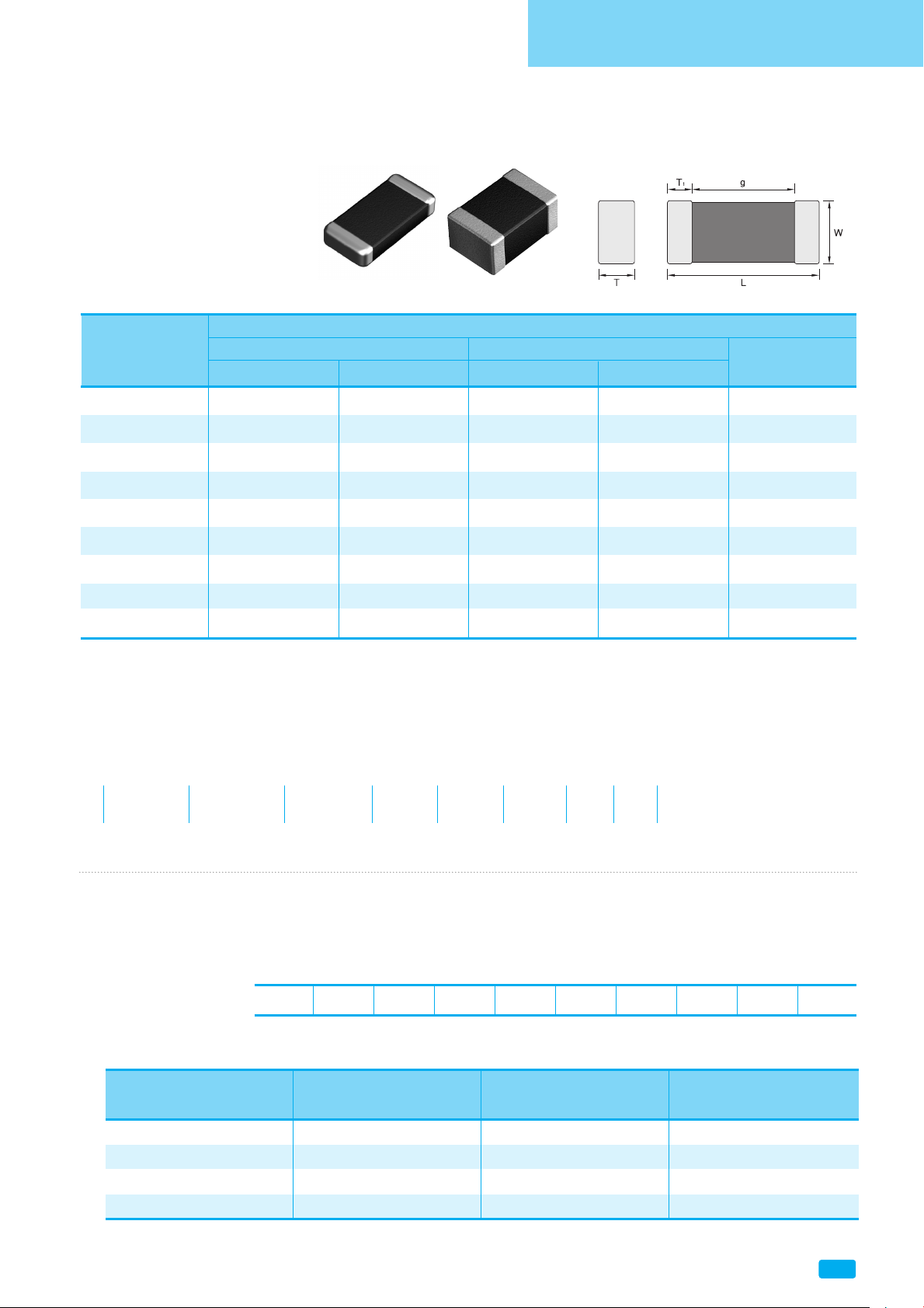
SMD Type
Multi Layer Ceramic Capacitors
5
Shape & Dimensions
Dimensions
Code(inch) Length Width
L Tol(±) W Tol(±)
T1(min)
0603(0201) 0.60 0.03 0.30 0.03 0.05
1005(0402) 1.00 0.05 0.50 0.05 0.05
1608(0603) 1.60 0.15 0.80 0.10 0.10
2012(0805) 2.00 0.20 1.25 0.15 0.10
3216(1206) 3.20 0.30 1.60 0.20 0.15
3225(1210) 3.20 0.40 2.50 0.25 0.15
4520(1808) 4.50 0.40 2.00 0.25 0.20
4532(1812) 4.50 0.40 3.20 0.30 0.20
5750(2220) 5.70 0.50 5.00 0.40 0.30
(Unit : mm)
CS 1608 X7R 104 K 160 N R B
How to Order(Product Identification)
Type
CS : SMD
SA : ARRAY
Size Code
This is expressed in tens of a millimeter.
The first two digits are the length, the last two digits are width.
Size
(mm)
0603 1005 1608 2012 3216 3225 4520 4532 5750
SMD Type
*1608 Size ≥ 10㎌⇒W : 0.8±0.15, T : 0.8±0.15
Temperature Coefficient Code
Temperature Temperature Capacitance Change or Operating
Characteristice Range Temperature Coefficient Temperature Range
C0G -55 to 125℃ 0±30ppm/℃-55 to 125℃
X7R -55 to 125℃±15% -55 to 125℃
X5R -55 to 85℃±15% -55 to 85℃
Y5V -30 to 85℃+22, -82% -30 to 85℃
Page 3
www.samwha.com
Multi Layer Ceramic Capacitors
SAMWHA CAPACITOR Co., Ltd.
6
Capacitance Tolerance Code
Code Tolerance Code Tolerance
B ±0.1pF M ±20%
C ±0.25pF P +100, -0%
D ±0.5pF Z +80, -20%
F ±1.0% H +0.25/-0pF
G ±2.0% I +0/-0.25pF
J ±5% U +5/-0%
K ±10% V +0/-5%
Voltage Code
Code 6R3 100 160 250 500 101 201 251 631 302
Vol. DC 6.3V DC 10V DC 16V DC 25V DC 50V DC 100V DC 200V DC 250V DC 630V DC 3000V
Capacitance Code(Pico Farads)
The nominal capacitance value in pF is expressed by three digit numbers.
The first two digits represents significant figures and the last digit denotes the number of zero
Ex.) 104 = 100000pF R denotes decimal 8R2 = 8.2pF
Termination Code
Ex.) N : Ni-Sn (Nickel-Tin Plate)
Packing Code
Ex.) R : Reel Type B : Bulk Type
Thickness Option
Thickness(mm)
Code
Thickness(mm)
Code
t Tol(±) t Tol(±)
0.30 0.03 Blank 1.30 0.20 E
0.50 0.05 Blank 1.35 0.20 H
0.60 0.10 A 1.60 0.20 I
0.80 0.10 B 1.80 0.20 J
0.85 0.15 B 2.00 0.25 K
1.00 0.15 E 2.50 0.25 L
1.10 0.15 E 2.80 0.30 M
1.15 0.15 E 3.20 0.30 N
1.25 0.15 E 5.00 0.40 O
Page 4
Multi Layer Ceramic Capacitors
7
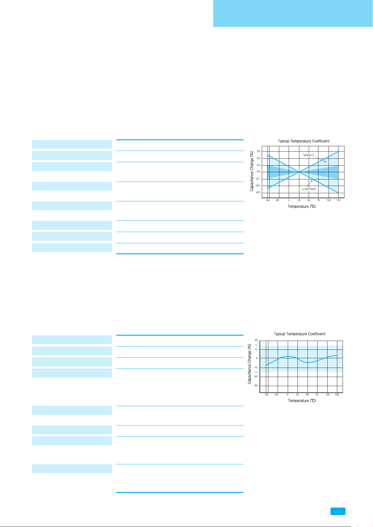
Typical Performance Characteristics
COG
Application
Suited for precision circuits, requiring stable dielectric characteristics, negligible dependence of capacitance and
dissipation factor on time, voltage and frequency.
Dielectric Characteristics
Temperature Characteristic 0±30ppm/℃
Operating Temperature -55~125℃
Capacitance Tolerance 10pF : ±5%, ±10%, (±1%, ±2%, ±20%)
≤10pF : ±0.1pF, ±0.25pF, ±0.5pF
Dissipation Factor & Q ≥30pF : DF≤0.1%, Q≥1000
30pF : Q≥400+20×C
Insulation Resistance More than 10,000MΩor 500ΩF
(Whichever is smaller)
Dielectric Strength 3×RVDC
Test Voltage 0.5 to 5Vrms(≤1000pF), 1±0.2Vrms(>1000pF)
Test Frequency 1±0.1M㎐(≤1000pF), 1±0.1k㎐(>1000pF)
Application
Stable class Ⅱdielectric properties, suited for by-pass and coupling purposes, filtering, frequency discrimination, DC
blockage, and as voltage transient suppression elements.
Dielectric Characteristics
Temperature Characteristic ±15%
Operating Temperature -55~125℃
Capacitance Tolerance ±10%, ±20%, (±5%, +80~-20%)
Dissipation Factor & Q 50V Min. : 2.5% Max. 25V Min. : 3.0% Max.
16V Min. : 3.5% Max. 10V Min. : 5.0% Max.
6.3V Min.
: 5.0% Max.
(<3.3㎌), 10% Max.(≥3.3㎌)
Thin layer lange capacitors type 10% Max.
Insulation Resistance
More than 10,000MΩor 500ΩF(Whichever is smaller)
Thin layer lange capacitors type
50ΩF
Min.
Dielectric Strength >2.5×RVDC
Test Voltage 1±0.2Vrms(≤10㎌, 10V Min.)
0.5±0.1Vrms(≤10㎌, 6.3V Max.)
0.5±0.1Vrms(>10㎌)
Test Frequency 1±0.1k㎐(≤10㎌, 10V Min.)
1±0.1k㎐(≤10㎌, 6.3V Max.)
120±24㎐(>10㎌)
X7R
SMD Type
Page 5
www.samwha.com
Multi Layer Ceramic Capacitors
SAMWHA CAPACITOR Co., Ltd.
8
Application
Stable class Ⅱdielectric properties, suited for by-pass and coupling purposes, filtering, frequency discrimination, DC
blockage, and as voltage transient suppression elements.
Dielectric Characteristics
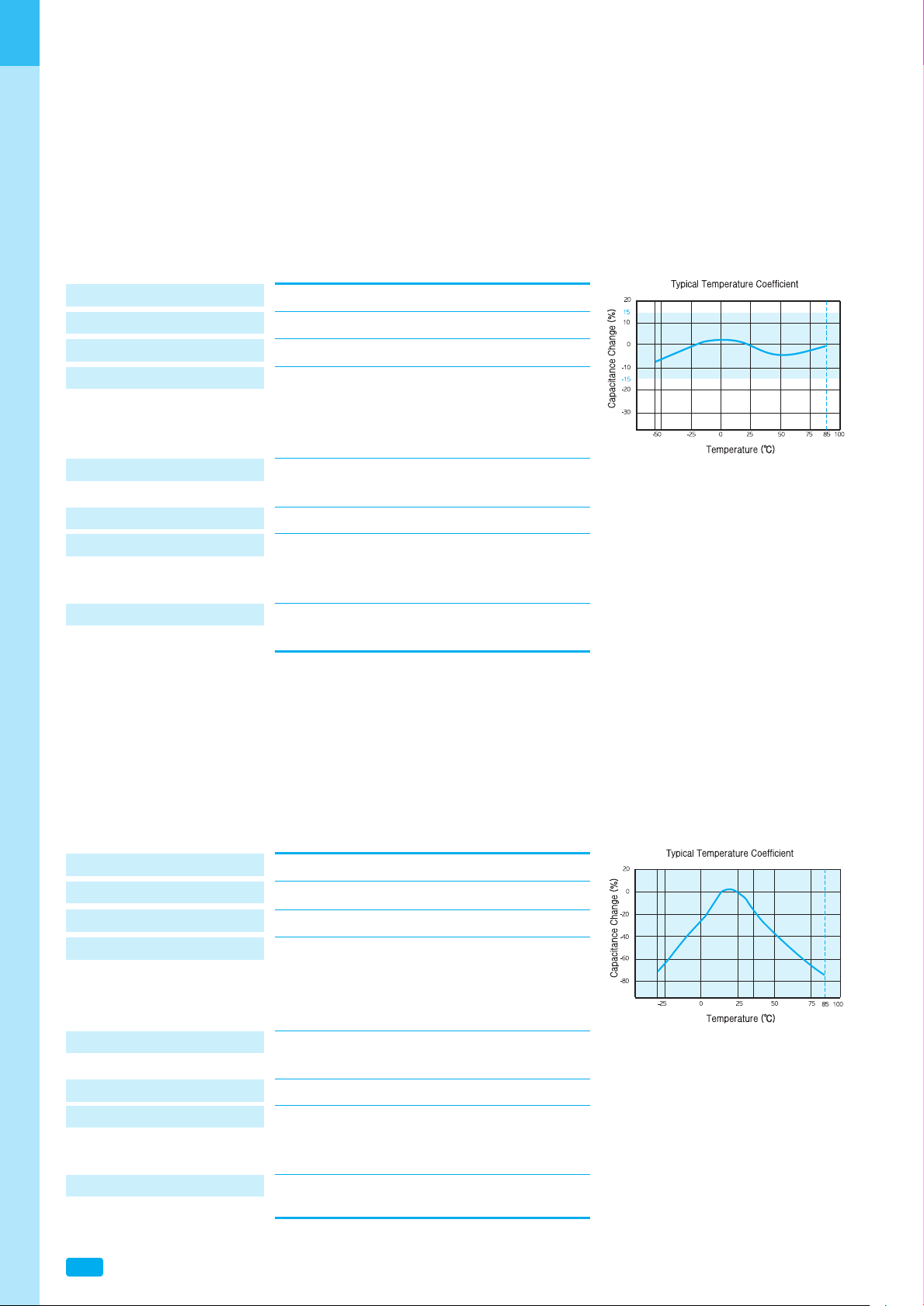
Temperature Characteristic ±15%
Operating Temperature -55~85℃
Capacitance Tolerance ±10%, ±20%, (±5%, +80~-20%)
Dissipation Factor & Q 50V Min. : 2.5% Max. 25V Min. : 3.0% Max.
16V Min. : 3.5% Max. 10V Min. : 5.0% Max.
6.3V Min.
: 5.0% Max.
(<3.3㎌), 10% Max.(≥3.3㎌)
Thin layer lange capacitors type 10% Max.
Insulation Resistance
More than 10,000MΩ or 500ΩF(Whichever is smaller)
Thin layer lange capacitors type
50ΩFMin.
Dielectric Strength >2.5×RVDC
Test Voltage 1±0.2Vrms(≤10㎌, 10V Min.)
0.5±0.1Vrms(≤10㎌, 6.3V Max.)
0.5±0.1Vrms(>10㎌)
Test Frequency 1±0.1k㎐(≤10㎌, 10V Min.)
1±0.1k㎐(≤10㎌, 6.3V Max.), 120±24㎐(>10㎌)
X5R
Application
The Hi-K(Y5V) dielectrics deliver high capacitance density and are ideally suited for applications where space is at a
premium, or as replacement for tantalum capacitors. Typically applications include use as by-pass or decoupling elements.
Best performance is obtained at or near room temperature, with low DC bias.
Dielectric Characteristics
Temperature Characteristic +22%~-82%
Operating Temperature -30~85℃
Capacitance Tolerance -20~+80%(±20%)
Dissipation Factor & Q 50V Min. : 5% Max. 25V Min. : 7% Max.
16V Min. : 9% Max. 10V Min. : 12.5% Max.
6.3V Min.
: 15% Max.
Thin layer lange capacitors type 20% Max.
Insulation Resistance
More than 10,000MΩor 500ΩF(Whichever is smaller)
Thin layer lange capacitors type
50
ΩF
Min.
Dielectric Strength >2.5×RVDC
Test Voltage 1±0.2Vrms(≤10㎌, 10V Min.)
0.5±0.1Vrms(≤10㎌, 6.3V Max.)
0.5±0.1Vrms(>10㎌)
Test Frequency 1±0.1k㎐(≤10㎌, 10V Min.)
1±0.1k㎐(≤10㎌, 6.3V Max.), 120±24㎐(>10㎌)
Y5V
Page 6
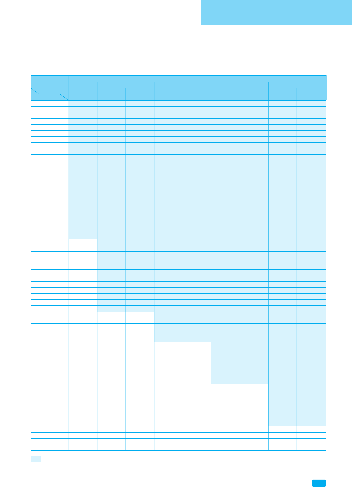
Multi Layer Ceramic Capacitors
9
Type
C0G
Size(inch) 0603(0201) 1005(0402) 1608(0603) 2012(0805) 3216(1206)
25 25 50 25 50 25 50 25 50
Cap.
0.5㎊(0R5)
1㎊(010)
2㎊(020)
3㎊(030)
4㎊(040)
5㎊(050)
6㎊(060)
7㎊(070)
8㎊(080)
9㎊(090)
10㎊(100)
12㎊(120)
15㎊(150)
18㎊(180)
22㎊(220)
27㎊(270)
33㎊(330)
39㎊(390)
47㎊(470)
56㎊(560)
68㎊(680)
82㎊(820)
100㎊(101)
120㎊(121)
150㎊(151)
180㎊(181)
220㎊(221)
270㎊(271)
330㎊(331)
390㎊(391)
470㎊(471)
560㎊(561)
680㎊(681)
820㎊(821)
1000㎊(102)
1200㎊(122)
1500㎊(152)
1800㎊(182)
2200㎊(222)
2700㎊(272)
3300㎊(332)
3900㎊(392)
4700㎊(472)
5600㎊(562)
6800㎊(682)
8200㎊(822)
10000㎊(103)
12000㎊(123)
15000㎊(153)
18000㎊(183)
22000㎊(223)
27000㎊(273)
33000㎊(333)
47000㎊(473)
56000㎊(563)
68000㎊(683)
82000㎊(823)
0.1㎌(104)
C0G-Temperature Compensating Type(0603~3216)
Appendix Ⅰ
SMD Type
Volt(V)
Temperature Compensating Type : Dissipation Factor Page 22 (No.5)
Page 7
www.samwha.com
Multi Layer Ceramic Capacitors
SAMWHA CAPACITOR Co., Ltd.
10
Type
Size(inch)
Cap.
100㎊(101)
470㎊(471)
1000㎊(102)
2200㎊(222)
4700㎊(472)
10000㎊(103)
15000㎊(153)
22000㎊(223)
33000㎊(333)
47000㎊(473)
68000㎊(683)
0.1㎌(104)
0.15㎌(154)
0.22㎌(224)
0.33㎌(334)
0.47㎌(474)
0.68㎌(684)
1.0㎌(105)
1.5㎌(155)
2.2㎌(225)
4.7㎌(475)
6.8㎌(685)
10㎌(106)
22㎌(226)
47㎌(476)
100㎌(107)
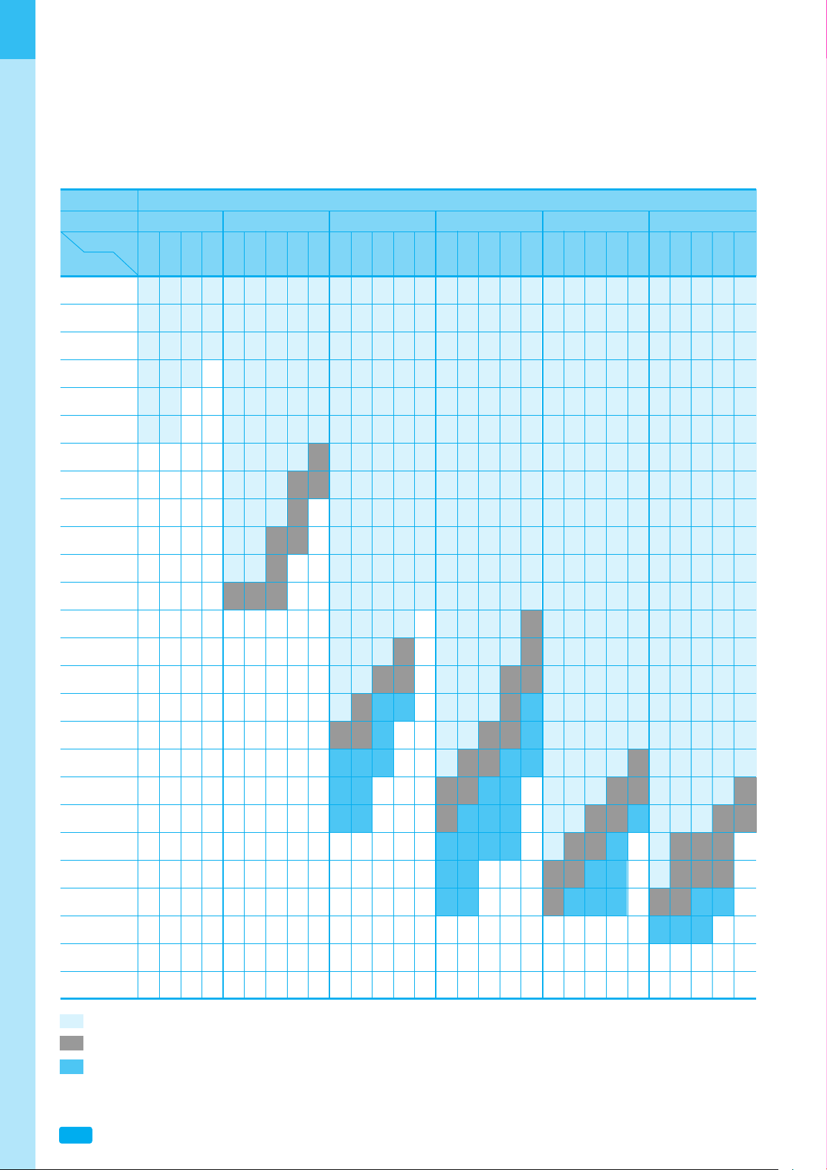
X7R-High Dielectric Constant Type(0603~3225) & Thin Layer Large-Capacitance Type
X7R
Appendix Ⅱ
0603(0201) 1005(0402) 1608(0603) 2012(0805) 3216(1206) 3225(1210)
6.3 10 16 25 6.3 10 16 25 50 6.3 10 16 25 50 6.3 10 16 25 50 6.3 10 16 25 50 6.3 10 16 25 50
General Type : Dissipation Factor Page 22 (No.5)
General Type : Dissipation Factor Page 22 (No.5)
Thin Layer Large-Capacitance Type : Dissipation Factor Page 22 (No.5)
Volt(V) Volt(V)
Page 8
Multi Layer Ceramic Capacitors
11
SMD Type
Type
Size(inch)
Cap.
100㎊(101)
470㎊(471)
1000㎊(102)
2200㎊(222)
4700㎊(472)
10000㎊(103)
15000㎊(153)
22000㎊(223)
33000㎊(333)
47000㎊(473)
68000㎊(683)
0.1㎌(104)
0.15㎌(154)
0.22㎌(224)
0.33㎌(334)
0.47㎌(474)
0.68㎌(684)
1.0㎌(105)
1.5㎌(155)
2.2㎌(225)
4.7㎌(475)
6.8㎌(685)
10㎌(106)
22㎌(226)
47㎌(476)
100㎌(107)
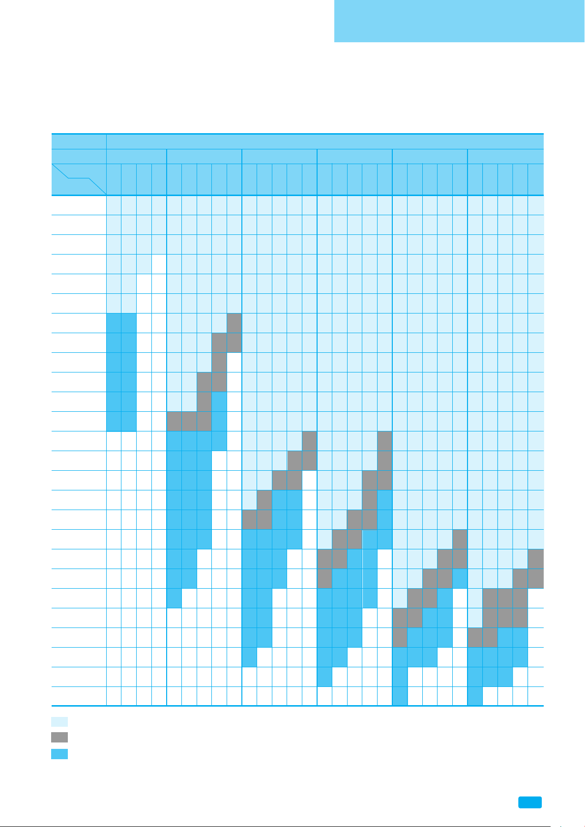
X5R-High Dielectric Constant Type(0603~3225) & Thin Layer Large-Capacitance Type
X5R
0603(0201) 1005(0402) 1608(0603) 2012(0805) 3216(1206) 3225(1210)
6.3 10 16 25 6.3 10 16 25 50 6.3 10 16 25 50 6.3 10 16 25 50 6.3 10 16 25 50 6.3 10 16 25 50
General Type : Dissipation Factor Page 22 (No.5)
General Type : Dissipation Factor Page 22 (No.5)
Thin Layer Large-Capacitance Type : Dissipation Factor Page 22 (No.5)
Page 9
www.samwha.com
Multi Layer Ceramic Capacitors
SAMWHA CAPACITOR Co., Ltd.
12
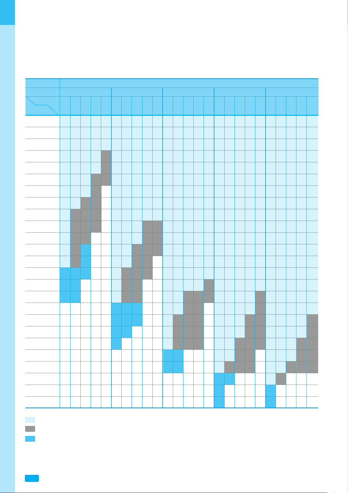
Y5V-High Dielectric Constant Type(0603~3225) & Thin Layer Large-Capacitance Type
Y5V
1005(0402) 1608(0603) 2012(0805) 3216(1206) 3225(1210)
6.3 10 16 25 50 6.3 10 16 25 50 6.3 10 16 25 50 6.3 10 16 25 50 6.3 10 16 25 50
General Type : Dissipation Factor Page 22 (No.5)
General Type : Dissipation Factor Page 22 (No.5)
Thin Layer Large-Capacitance Type : Dissipation Factor Page 22 (No.5)
Type
Size(inch)
Cap.
1000㎊(102)
2200㎊(222)
4700㎊(472)
10000㎊(103)
15000㎊(153)
22000㎊(223)
33000㎊(333)
47000㎊(473)
68000㎊(683)
0.1㎌(104)
0.15㎌(154)
0.22㎌(224)
0.33㎌(334)
0.47㎌(474)
0.68㎌(684)
1.0㎌(105)
1.5㎌(155)
2.2㎌(225)
3.3㎌(335)
4.7㎌(475)
6.8㎌(685)
10㎌(106)
22㎌(226)
47㎌(476)
100㎌(107)
Volt(V)
Page 10

Multi Layer Ceramic Capacitors
13
SMD Type-High Voltage
Product Offering
SAMWHA high voltage MLCC products with the temperature characteristics of C0G and X7R are designed
for commercial and industrial applications. The products are applied to DC-DC converters and ballast
circuit to reduce ripple noise and diverting potentially unsafe transients in various sizes with working
voltage up to DC 7kV. These high voltage capacitors feature a special internal electrode design which has
capacitor network to reduce voltage concentrations by distributing voltage throughout the entire capacitor.
Features
High reliability
The highest voltage rating by the special internal electrode design
Wide voltage level : from 100VDCto 7,000V
DC
Surface mount suited for wave and reflow soldering
RoHS compliant
Applications
DC-DC Converters
Network Equipments
Back-Lighting Inverter
Lighting Ballast
Modem & Power Supply
LAN/WLAN Interface
※ special specification like a Automobile, Medical, Military, Aviation should be discuss with our sales representatives
Special Options for the Safety
Inset electrode margins to prevent short mode failure resulted from the crack by mechanical bending
stress
Soft termination is optionally available to reduce possibility for the crack of MLCCs by mechanical
bending stress
SMD Type-High Voltage
Page 11
www.samwha.com
Multi Layer Ceramic Capacitors
SAMWHA CAPACITOR Co., Ltd.
14
Tolerance
Code Tolerance Code Tolerance
B
±
0.1pF C
±
0.25pF
D
±
0.50pF F
±
1%
G
±
2% J
±
5%
K
±
10% M
±
20%
Z +80~-20%
Thickness Option
Rated Voltage Code
1st two digits are value, 3rd digit denotes number of zeros; 302 = 3,000V, 502 = 5,000V, 722 = 7,200V
Plating Packing
Ni / Sn Plated B : Bulk Pack R : Reel Pack C : Case Box
Thickness(mm)
Code
Thickness(mm)
Code
t Tol(±) t Tol(±)
0.60 0.10 A 1.35 0.20 H
0.80 0.10 B 1.60 0.20 I
0.85 0.15 B 1.80 0.20 J
1.00 0.15 E 2.00 0.25 K
1.10 0.15 E 2.50 0.25 L
1.15 0.15 E 2.80 0.30 M
1.25 0.15 E 3.20 0.5 N
1.30 0.20 E 5.00 0.5 O
Dielectric (Temp. Coefficient)
COG, X7R
Capacitance
1st two digits are value, 3rd digit denotes number of zeros;
331 = 330pF, 104 = 100000pF, 8R2 = 8.2pF
Size
(mm)
1608 2012 3216 3225 4520 4532 5750 7566 9595
CS 4520 COG 150 J 302 N R E
How to Order(Product Identification)
Type
CS : SMD
Size Code
Page 12
Multi Layer Ceramic Capacitors
15
SMD Type-High Voltage
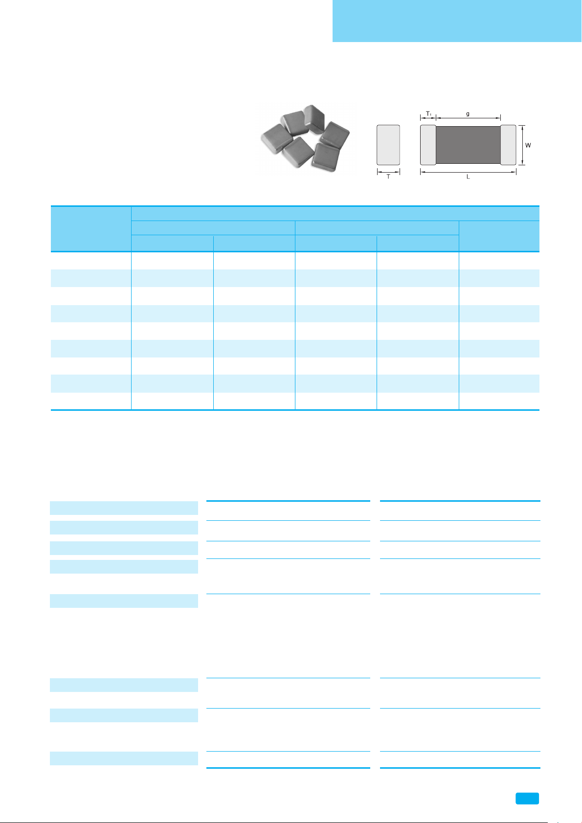
Dielectric Characteristics
Dielectric Classification Ultra Stable Stable
Rated temperature range -55℃ to +125℃-55℃ to +125℃
TCC
(Temperature Characteristics Coefficient)
0±30ppm ±15%
Dissifation Factor(tan δ)C≥30pF : Q≥1,000 (DF:≤ 0.1%) 2.5% Max.
C<30pF :
Q≥400+20C(DF: ≤1/(400+20C))
IR(Insulation Resistance) 500V Below : Rated voltage 60sec 500V Below:Rated voltage 60sec
500V Above : 500V 60sec 500V Above:500V 60sec
More than 10,000 ㏁ -DC100V~1KV
:C≥0.01㎌:More than 100㏁㎌
:C<0.01㎌:More than 10,000㏁
-DC2~3KV:More than6,000 ㏁
Capacitance Tolerance <10pF : ±0.25pF, ±0.5pF ±10%, ±20%
≥10pF : ±5%, ±0%
Dielectric strength 630V:150% Rated Voltage 100V:150% Rated Voltage
1kV~7.2kV:120% Rated Voltage 630V:150% Rated Voltage
1kV~7.2kV: 120% Rated Voltage
Aging characteristics 0% 2.5% per decade hr, typical
Typical Performance Characteristics
COG(NPO) X7R
Dimensions
Code Length Width
L Tol(±) W Tol(±)
T1(min)
1608(0603) 1.60 0.15 0.80 0.10 0.10
2012(0805) 2.00 0.20 1.25 0.15 0.10
3216(1206) 3.20 0.30 1.60 0.20 0.15
3225(1210) 3.20 0.40 2.50 0.25 0.15
4520(1808) 4.50 0.40 2.00 0.25 0.20
4532(1812) 4.50 0.40 3.20 0.30 0.20
5750(2220) 5.70 0.50 5.00 0.40 0.30
7566(3026) 7.50 0.50 6.60 0.50 0.30
9595(3838) 9.50 0.50 9.50 0.50 0.30
(Unit : mm)
Shape & Dimensions
*1608 Size ≥ 10㎌⇒W : 0.8±0.15, T : 0.8±0.15
Page 13
Page 14
Page 15
SAMWHA CAPACITOR Co., Ltd.
18
www.samwha.com
Multi Layer Ceramic Capacitors
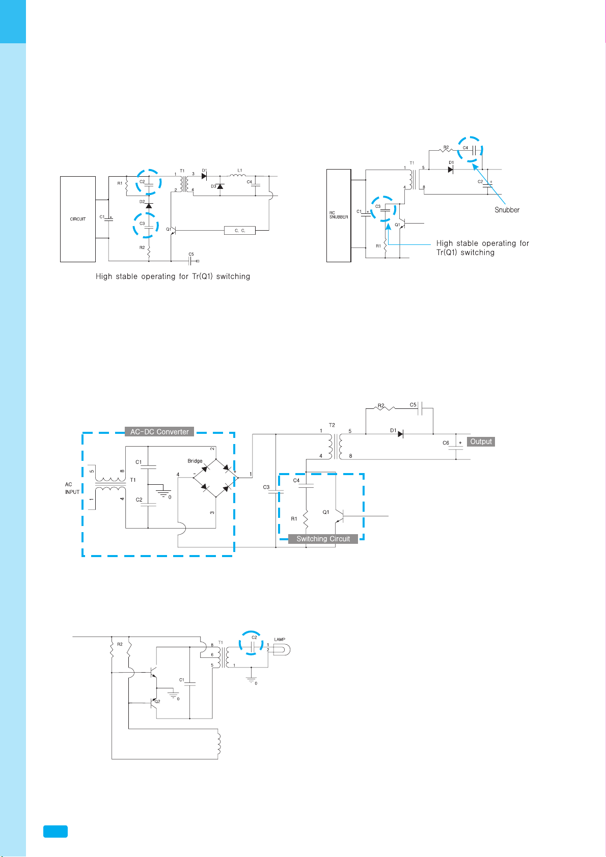
Application(Typical circuit)
DC-DC Converter
Primary circuit and Snubber switching power supply
LCD back light Inverter
Switching Power Supply
C2 : X7R ; 250V 10nF~47nF
C3 : COG ; 630V 47pF~100pF
C3 : COG, X7R ; 2kV 100pF~1000pF
C4 : COG, X7R ; 2kV 100pF~1000pF
C1, C2 : COG or X7R 1000pF~4700pF
C4 : COG ; 2kV 100pF~330pF
C5 : COG ; 1kV/2kV 100pF~470pF
C2 : COG ; 3kV 10 ~100pF
Page 16
Multi Layer Ceramic Capacitors
19
SMD Type-High Voltage
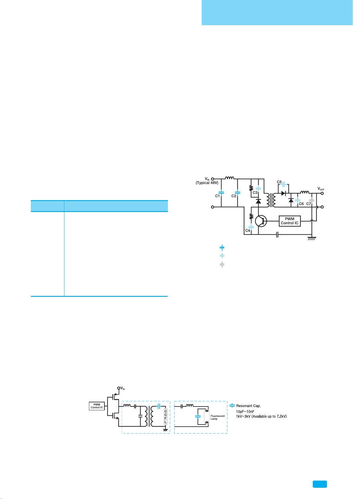
MLCC Applications for DC-DC Converter Modules
MLCC Applications for Ballast Circuits
High voltage MLCCs are mainly used to DC-DC converter modules for industrial applications which have high input
voltage of typical 48V. These are used as functions of high frequency noise filtering (decoupling) of power line and
snubber capacitor to protect switching device from unsafe transients by inductance of transformer or connection line
due to switching operation. For these applications, MLCCs have merits for high allowable ripple current and high
reliability.
Figure 2 shows isolated DC-DC converter circuit diagram and MLCC applications such as decoupling and snubber.
Input voltage is 36~75VDC(typical 48VDC) for general industrial applications such as base station, server and network
equipments. Decoupling MLCCs are applied to input and output (based on viewpoint of switch or transformer)
power line to reduce ripple voltage, and MLCCs for snubber application used to absorb surge energy. SAMWHA
MLCCs are recommended for each application as shown in Table 1.
Table 1. MLCC recommendation for isolated
type DC-DC converter module
Items MLCC Recommendation
*Input 1210 X7R 470nF 100V
(C1, C2) 1812 X7R 1.0uF 100V
Snubber Available wide range of products
(C3~C6) 250V ~2kV (Available up to 7.2 kV)
100pF~2.2nF (Available up to 470nF)
Output (High Capacitance Application)
(C7) 1210 X5R 100uF 6.3V
1206 X5R 47uF 6.3V
0805 X5R 47uF 6.3V
Input Decoupling MLCC (~1.0uF 100V)
Snubber Cap. (100pF~2.2nF 250V~2kV)
Output Decoupling MLCC (10~100uF 6.3V
*Typical input voltage of 48V for industrial application
Fig. 3. Typical electronic ballast circuit and MLCC application
High voltage MLCCs are suitable for the ballast circuit as a function of resonant capacitor as presented in Figure 3.
MLCCs with high voltage rating from 1kV to 3kV (available up to 7.2kV) are mainly used for these application.
SAMWHA offers wide range of capacitance and rated voltage with high reliability.
Page 17
SAMWHA CAPACITOR Co., Ltd.
20
www.samwha.com
Multi Layer Ceramic Capacitors
Caution(Rating)
1. Operating Voltage
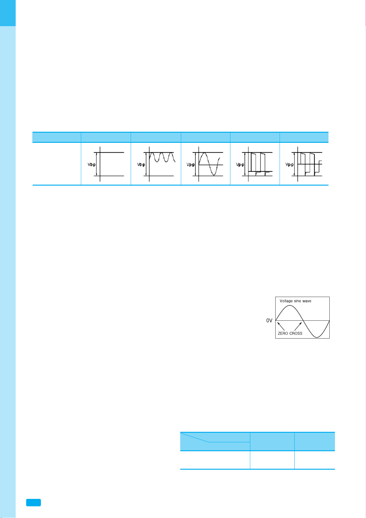
When DC-rated capacitors are to be used in AC or ripple current circuits, be sure to maintain the Vp-p Value of the
applied voltage or the Vo-p which contains DC bias within the rated voltage range.
When the voltage is applied to the circuit, starting or stopping may generate irregular voltage for a transit period
because of resonance or switching. Be sure to use a capacitor with a rated voltage range that includes these
irregular voltages.
2. Test condition for AC withstanding Voltage
(1) Test Equipment
Tests for AC withstanding voltage should be made with equipment capable of creating a wave similar to a 50/60
Hz sine wave. If the distorted sine wave or overload exceeding the specified voltage value is applied, a defect
may be caused.
(2) Voltage applied method
The capacitor's leads or terminals should be firmly connected to the output of the withstanding voltage test
equipment, and then the voltage should be raised from near zero to the test voltage. If the test voltage is applied
directly to the capacitor without raising it from near zero,it should be applied with the
*zero cross. At the end of the test time, the test voltage should be reduced to near
zero, and then the capacitor's leads or terminals should be taken off the output of the
withstanding voltage test equipment. If the test voltage is applied directly to the
capacitor without raising it from near zero, surge voltage may occur and cause a
defect. *ZERO CROSS is the point where voltage sine wave
(3) Dielectric strength testing method
In case of dielectric strength test, the capacitor’s is applied between the terminations for 1 to 5 sec., provided the
charge/discharge current is less than 50mA.
3. Soldering
If a chip component is heated or cooled abruptly during soldering, it may crack due to the thermal shock. To
prevent this, follow our recommendations below for adequate soldering conditions. Carefully perform preheating
so that temperature difference (ΔT) between the
solder and component surface is in the following
range. The smaller the temperatures difference (Δ
T) between the solder and component surface is,
the smaller the influence on the chip is.
Voltage
Positional
Measurement
DV Voltage DC+AC Voltage AC Voltage Pulse Voltage(1) Pulse Voltage(2)
Chip Size
3.2×1.6mm 3.2×2.5mm
Slodering Method and under and over
Reflow Method or
ΔT 190℃ΔT130℃
Soldering Lron Method
Page 18
Multi Layer Ceramic Capacitors
21
SMD Type-High Voltage
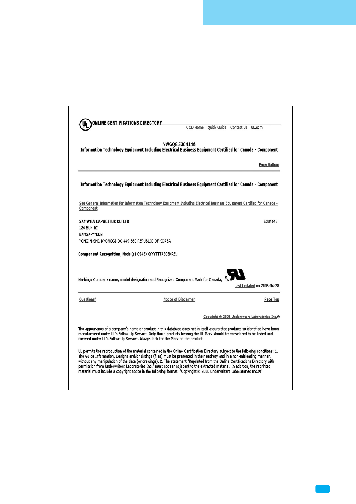
SAMWHA CAPACITOR CO., LTD offers a line of MLCC(Multilayer Ceramic Capacitor).
These parts are rated at 3kV dc and safety approved and certified to UL
(Underwriters Laboratories Inc. )
Page 19
SAMWHA CAPACITOR Co., Ltd.
22
www.samwha.com
Multi Layer Ceramic Capacitors
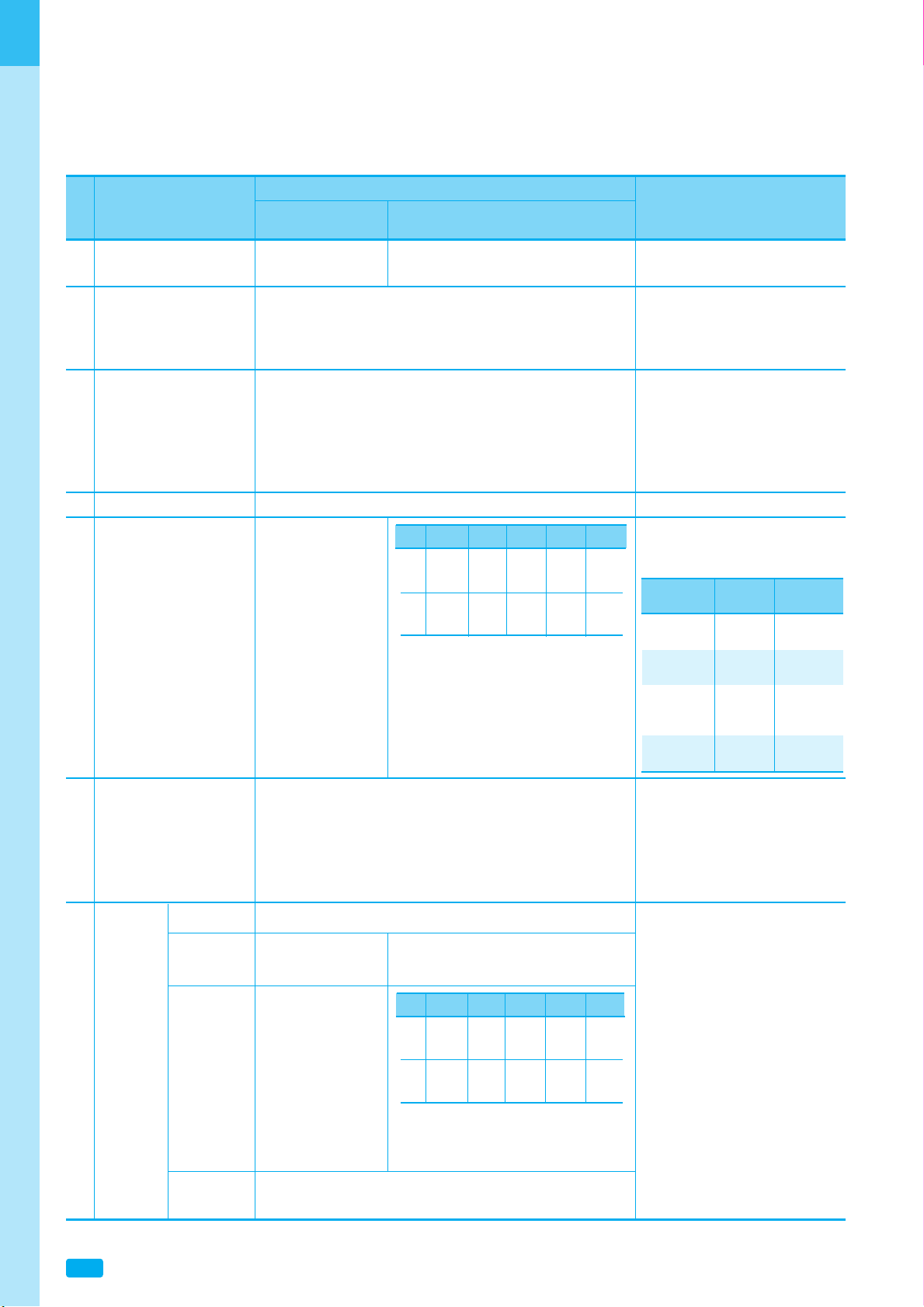
Reliability and Test Conditions(General Type)
No.
Item
Characteristic
Temperature
Compensating Type
High Dielectric Constant Type
Test Methods
and Conditions
1 Operating X7R : -55 to +125℃ X5R : -55 to +85℃
Temperature Range
C0G : -55 to +125℃
Y5V : -30 to +85℃
2 Insulation Resistance More than 10,000
MΩ or 500ΩF(Whichever is smaller)
3 Dielectric Strength No defects or abnormalities
4 Capacitance Within the specified tolerance
5 Dissipation Factor 30㎊ Min. :
Q≥1,000 (DF≤0.1%)
30㎊ Max. :
Q≥400+20C
(DF≤1/(400+20C))
6 Solderability of Termination should be covered with more than - Pb-Free Type
Termination 75% of new solder Solder : 96.5Sn-3Ag-0.5Cu
Solder Temperature : 260
±
5℃
Immersion Time : 3±0.1sec
- Pre-Heating
at 80~120℃ for 10~30sec
7 Appearance No marked defect
Capacitchange
Within ±
2.5% or ±0.25㎊
X7R, X5R : ≤±7.5%
(whichever is larger) Y5V : ≤±20%
Dissipation
Factor
(or Q)
I.R. More than 10,000
MΩ or 500Ω.F (Whichever is smaller)
Char.
50V Min.
25V 16V 10V 6.3V
X7R ≤2.5%/≤3%/≤3.5%/≤5%/≤5%/
X5R ≤5% ≤7% ≤7% ≤10% ≤10%
Y5V
≤
5%/≤7%/≤9% ≤
12.5%/
≤
15%
≤
9% ≤9%
≤
12.5%
≤
15%
Char.
50V Min.
25V 16V 10V 6.3V
X7R ≤2.5%/≤3%/≤3.5%/≤5%/≤5%/
X5R
≤
5% ≤7% ≤7% ≤10% ≤10%
Y5V
≤
5%/≤7%/≤9% ≤
12.5%/
≤
15%
≤
9% ≤9%≤
12.5%≤
15%
Cap.
Testing Testing
Frequency Voltage
C0G
1±
0.1M
㎐
0.5 to 5V
rms
(C≤1000pF)
C0G
1±0.1k㎐ 1±0.2Vrms
(C >1000pF)
X7R, X5R, Y5V
(C≤10㎌ 1±0.1k㎐ 1±0.2Vrms
6.3V Min.)
X7R, X5R, Y5V
(C >10㎌)
120±24㎐
0.5±0.1Vrms
Resistance
to
Soldering
Heat
30㎊ Min. :
Q≥1,000 (DF≤0.1%)
30㎊ Max. :
Q≥400+20C
(DF≤1/(400+20C))
- Preheat the capacitor at 120 to 150℃
for 1 minute. (Preheating for 3225,
4520, 4532 Step1 : 100℃ to 120℃, 1min
Step2 : 170℃ to 200℃, 1min) Immerse the
capacitor in a eutectic solder solution
- Soldering Temp. : 260±5℃
- Immersion Time : 10±0.5sec
- Initial measurement
Perform a heat treatment at 150+0, -10℃
for one hour and then let sit for 48±4
hours at room temperature.
Perform the intial measurement.
- Measurement after test
Take it out and set it for 24±2 hours
(temperature compensating type)
or 48±4 hours (high dielectric constant
type)then measure
- Applied the rated voltage for 2
minutes of charging.
- The charge/discharge current is
less than 50mA.
- C0G : The rated voltage×300%
- X7R, X5R, Y5V : 〃×250%
- Applied between the terminations
for 1 to 5 seconds.
- The charge/discharge current is
less than 50mA.
You can check the specification at
the appendix for each product
with mark
The capacitance/Q/D.F. should be
measured at 25℃ at the frequency
and voltage shown in the table.
Page 20
Multi Layer Ceramic Capacitors
23
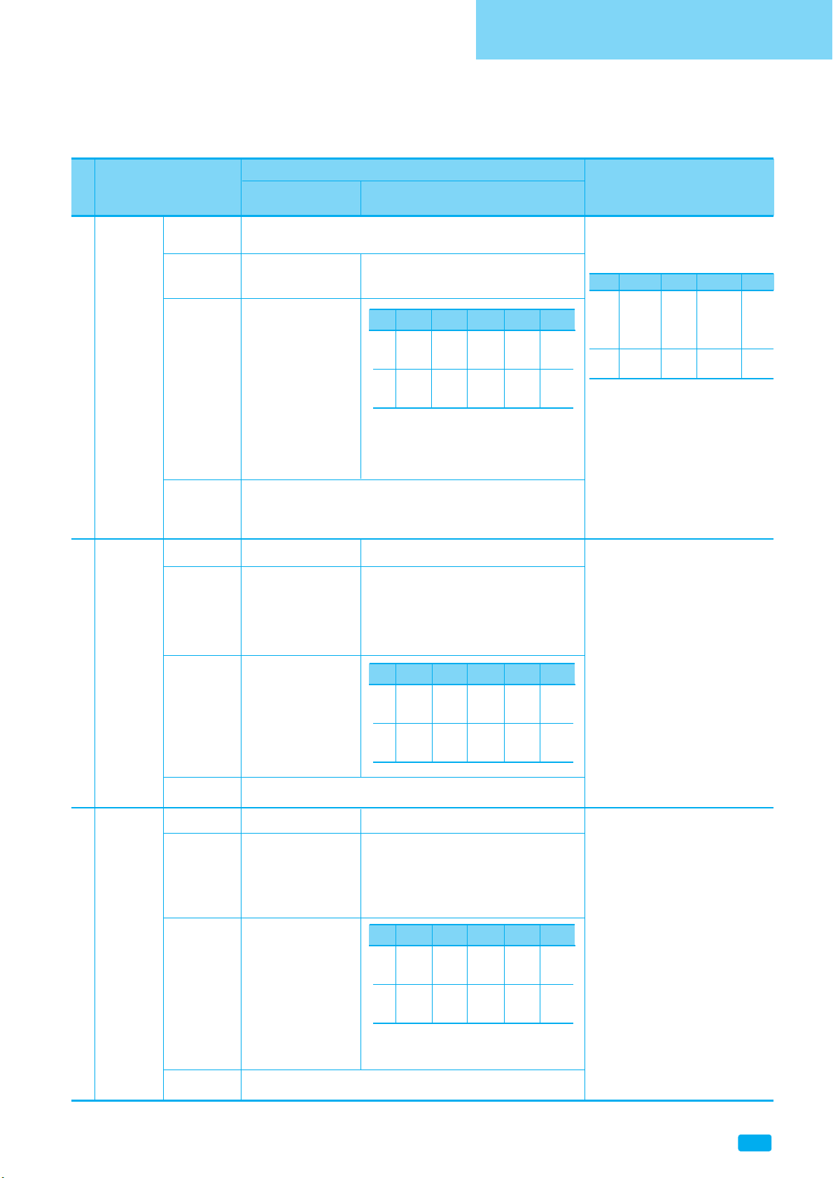
SMD Type
30㎊ Min. :
Q≥1,000 (DF≤0.1%)
30㎊ Max. :
Q≥400+20C
(DF≤1/(400+20C))
No.
Item
Characteristic
Temperature
Compensating Type
High Dielectric Constant Type
Test Methods
and Conditions
8
Temperature
Appearance
No marking defects
Cycle
Capacitance
Within ±2.5% or ±0.25㎊
X7R, X5R : Within ±7.5%
Change (whichever is larger) Y5V : Within
±
20%
Dissipation
Factor
(or Q)
I.R. More than 10,000
MΩor 500Ω.F(Whichever is smaller)
9
Humidity
Appearance
No marking defects
Load
Capacitance
Within ±7.5% or ±0.75㎊
X7R, X5R : Within ±12.5%
Change (whichever is larger) Y5V : Within
+
30%, -40%
(Y5V/1.0㎌, 2.2㎌, 4.7㎌/10V)
Within
±
30% (others)
I.R. More than 500
MΩor 25Ω.F(Whichever is smaller)
10
Appearance
No marking defects
Capacitance
Within ±3% or ±0.3㎊
X7R, X5R : Within ±12.5%
Change (whichever is larger) Y5V : Within
±
30%(Cap. < 1.0㎌)
Within
+
30%, -40%
(Cap. ≥ 1.0㎌)
Dissipation
Factor
(or Q)
I.R. More than 10,000
MΩ or 50Ω.F(Whichever & Smaller)
30㎊ Min. :
Q≥200 (DF≤0.5%)
30㎊ Max. :
Q≥100 +10/3C
(DF≤1/(100+10/3C))
30㎊ Min. :
Q≥350 (DF≤0.3%)
10㎊≤Cp ≤30
㎊:
Q≥275 +5/2C
(DF≤1/(275+5/2C))
10㎊ Max. :
Q≥200+10C
(DF≤1/(200+10C))
High
Temperature
Load
Char.
50V Min.
25V 16V 10V 6.3V
X7R ≤5%/≤5%/≤5%/≤7.5%/≤7.5%/
X5R ≤7.5% ≤10% ≤10% ≤12.5%≤
12.5%
Y5V
≤
7.5%/≤10%/≤12.5% ≤
15%/
≤
20%
≤
12.5%≤
12.5%≤
15%≤
20%
Char.
50V Min.
25V 16V 10V 6.3V
X7R ≤5%/≤5%/≤5%/≤7.5%/≤7.5%/
X5R ≤7.5% ≤10% ≤10% ≤12.5%≤
12.5%
Y5V
≤
7.5%/≤10%/≤12.5% ≤
15%/
≤
20%
≤
12.5%≤
12.5% ≤15%≤
20%
Char.
50V Min.
25V 16V 10V 6.3V
X7R ≤5%/≤5%/≤5%/≤7.5%/≤7.5%/
X5R ≤7.5% ≤10% ≤10%
≤
12.5%
≤
12.5%
Y5V
≤
7.5%/≤10%/≤12.5% ≤
15%/
≤
20%
≤
12.5%≤
12.5%≤
15%≤
20%
- Temperature : 40±2℃
- Humidity : 90~95%
- Hour : 500
±
12hrs
- Test Voltage : The rated voltage
- Take it out and set it for 24
±
2 hours
(temperature compensating) or
48
±
4 hours(high dielectric constant
type) at room temperature, then
measure.
The charge/discharge current is
less than 50mA
- Testing time : 1000
±
12hrs
- Applied voltage :
Rated voltage < DC250V : ×200%
- Temperature :
C0G, X7R → 125
±
3℃
X5R , Y5V → 85
±
3℃
- Measurement after test
Take it out and set it for 24±2
hours(temperature compensating
type)or 48±4 hours (high dielectric
constant type) at room temperature,
then measure.
The charge/discharge current is
less than 50mA.
Perform the five cycless according
to the four heat treatments listed in
the following table.
Step 1 2 3 4
Min. Max.
Temp.
Operating
Room
Operating
Room
(℃) Temp. Temp. Temp. Temp.
+0, -3 +3, -0
Time
30
±
3 2 to 3 30±3 2 to 3
(Min)
- Initial measurement
Perform a heat treatment at 150+0,
-10℃ for one hour and then let sit
for 48
±
4 hours at room temperature.
- Measurement after test
Take it out and set it for 24
±
2 hours
(temperature compensating) or
48
±
4 hours(high dielectric constant
type) at room temperature, then
measure.
Dissipation
Factor
(or Q)
Page 21
SAMWHA CAPACITOR Co., Ltd.
24
www.samwha.com
Multi Layer Ceramic Capacitors
No.
Item
Characteristic
Temperature
Compensating Type
High Dielectric Constant Type
Test Methods
and Conditions
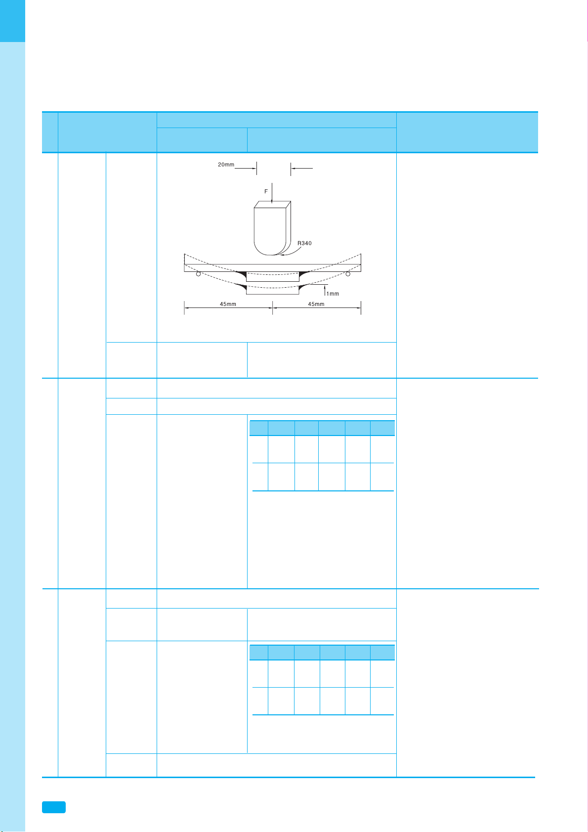
11 Bending
Strength
Capacitance Within ±5% or ±0.5
㎊
X7R, X5R : Within ±12.5%
Change (whichever is larger)
Y5V : Within ±30%
12
Appearance
No defects or abnormalities
Capacitance Whin the specified tolerance
- Substrate Material :
Glass EPOXY Board
- Board Thickness :
1.6mm
0.8mm(0603/1005size)
※ Test Condition
- Bending Limit : 1mm
- Pressurizing Speed : 1mm/sec
Shown in Fig. After soldering and
then let sit for 24+4hr(temperature
compensating type), 48±4hr (high
dielectric constant type) at room
temperature.
The capacitor should be subjected
to a simple harmonic motion having
a total amplitude of 1.5mm, the
frequency being varied uniformly
between the approximate limits of
10 and 55Hz, shall be traversed(from
10Hz to 55Hz then 10Hz again) in
approximately 1 minute.
This motion shall be applied for a
period of 2 hours in each 3mutually
perpendicular directions(total is
6hours).
- Temperature : 40±2℃
- Humidity : 90~95%
- Hour : 500±12hours
- Measurement after test
Take it out and set it for 24±2 hours
(temperature compensating type) or
48±4 hours(high dielectric constant
type) at room temperature, then
measure.
No cracking or marking defects shall occur
Vibration
Resistance
Char.
50V Min.
25V 16V 10V 6.3V
X7R ≤2.5%/≤3%/≤3.5%/≤5%/≤5%/
X5R ≤5% ≤7% ≤7% ≤10% ≤10%
Y5V
≤
5%/≤7%/≤9% ≤
12.5%/
≤
15%
≤
9% ≤9%≤
12.5%≤
15%
Char.
50V Min.
25V 16V 10V 6.3V
X7R ≤5%/≤5%/≤5%/≤7.5%/≤7.5%/
X5R ≤7.5% ≤10% ≤10%≤
12.5%≤
12.5%
Y5V
≤
7.5%/≤10%/≤12.5% ≤
15%/
≤
20%
≤
12.5% ≤12.5% ≤15%≤
20%
30㎊ Min. :
Q 1,000 (DF 0.1%)
30㎊ Max. :
Q 400+20C
(DF 1/ (400+20C))
30㎊ Min. :
Q≥350 (DF≤0.3%)
10
㎊
≤Cp ≤30
㎊:
Q≥275 +5/2C
(DF≤1/(275+5/2C))
10㎊ Max. :
Q≥200+10C
(DF≤1/(200+10C))
13 Humidity
Steady
State
Appearance
No marking defects
Capacitance Within ±5% or ±0.5
㎊
X7R, X5R : Within ±12.5%
Change (whichever is larger)
Y5V : Within ±30%
Dissipation
(or Q)
I.R
More than 1,000
MΩor 50Ω.F (Whichever is Smaller)
Q/DF
Page 22
Multi Layer Ceramic Capacitors
25
SMD Type
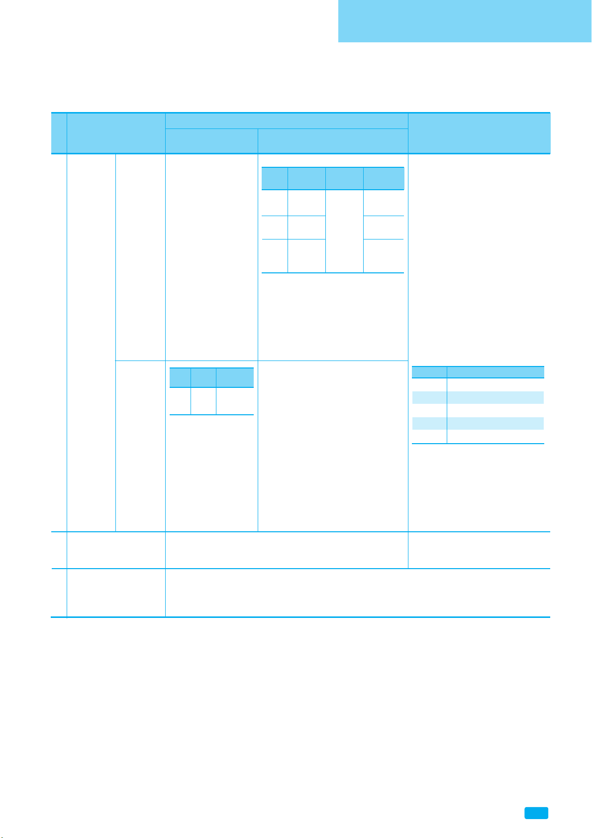
Char.
Temp. Reference Cap.
Range Temp. Change
X7R
-55 to Within
+125
℃
±
15%
X5R
-55 to Within
+85
℃
±
15%
Y5V
-30 to
Within
+85
℃
22
%
-82%
Step Temperature(℃)
125±2
2 -55±3
325±2
4 125±3(for C0G)
525±2
(1)
Temperature Compensating Type:
The temperature coefficient is
determined using the capacitance
measured in step 3 as a reference,
When cycling the temperature
sequentially from step 1 through 5,
(C0G: +25 to 125℃) the capacitance
shall be with in the specified
tolerance for the temperature
coefficient.
The capacitance drift is calculated
by dividing the difference
between the maximum measured
values in the step 1, 3 and 5 by the
Cap. value in step 3
(2) High Dielectric Constant Type :
The ranges of capacitance
change compared with the 25℃
value over the temperature
range shown in the table shall
be in the specified range.
15 Preservation(keeping) ※When solderability is considered, capacitors are
recommended to be used in 12 months
16 The regulation of ※Never use materials mentioned below in MLCC products regulated this document.
environmental Pb, Cd, Hg, Cr
+6
, PBB(polybrominated biphenyl), PBDE(polybrominated diphenyl ethers),
pollution materials. asbestos.
25
℃
No.
Item
Characteristic
Temperature
Compensating Type
High Dielectric Constant Type
Test Methods
and Conditions
14
Capacitance
Capacitance
Temperature
Change
Characteristics
Temperature
Coefficient
Char.
Temp.
Temperature
Range Coefficient
C0G
-55 to
±30ppm/℃
+125℃
(1) Temperature : 25℃±10℃
(2)
Relative Humidity : Below 70% RH
- In case of high Voltage and thin layer type Capacitor, it can be different from nomal specification.
So Please ask to our sales person.
Page 23
SAMWHA CAPACITOR Co., Ltd.
26
www.samwha.com
Multi Layer Ceramic Capacitors
Features
SAMWHA Series meet AEC-Q200 requirements
SAMWHA Series Certify ISO/TS 16949 and ISO 14001
SAMWHA Series are RoHS Compliant
Applications
Automotive electronic equipment
Automotive Applications
CQ 1608 X7R 104 K 500 N R B
How to Order(Product Identification)
Monolithic Multilayer Ceramic Capacitor Leadless Type for Automotive Application
Size Code
This is expressed in tens of a millimeter.
The first two digits are the length, The last two digits are width.
Temperature Coefficient Code
Classification Code Temperature Range Capacitance ToleranceClass
ClassⅠ C0G -55 to +125℃±30 ppm/℃
ClassⅡ X7R -55 to +125℃±15%
Capacitance Code(Pico farads)
The nominal capacitance value in pF is expressed by three digit numbers.
The first two digits represents significant figures and the last digit denotes the number of zero
Ex.) 104 = 100000pF
R denotes decimal
8R2 = 8.2pF
Page 24
Multi Layer Ceramic Capacitors
27
Automotive Applications
Capacitance Tolerance Code
Code Tolerance Code Tolerance
B ±0.1pF G ±2.0%
C ±0.25pF J ±5%
D ±0.5pF K ±10%
F ±1.0% M ±2.0%
Voltage Code
Code 6R3 100 160 250 500 101 201 251 501 631 102 202 302
Rated DC DC DC DC DC DC DC DC DC DC DC DC DC
Voltage 6.3V 10V 16V 25V 50V 100V 200V 250V 500V 630V 1KV 2KV 3KV
Termination Code
N : Nickel-Tin Plate A : Nickel-Tin Plate (Soft Termination)
Packing Code
R : Reel Type, B : Bulk Type
Thickness Option
Thickness(mm)
Code
Thickness(mm)
Code
t Tol(±) t Tol(±)
0.50 0.05 Blank 1.25 0.15 E
0.60 0.10 A 1.30 0.20 E
0.80 0.10 B 1.35 0.20 H
0.85 0.15 B 1.60 0.20 I
1.00 0.15 E 1.80 0.20 J
1.10 0.15 E 2.00 0.25 K
1.15 0.15 E 2.50 0.25 L
Temperature Characteristics
See Page 32 (No.21)
Page 25
SAMWHA CAPACITOR Co., Ltd.
28
www.samwha.com
Multi Layer Ceramic Capacitors
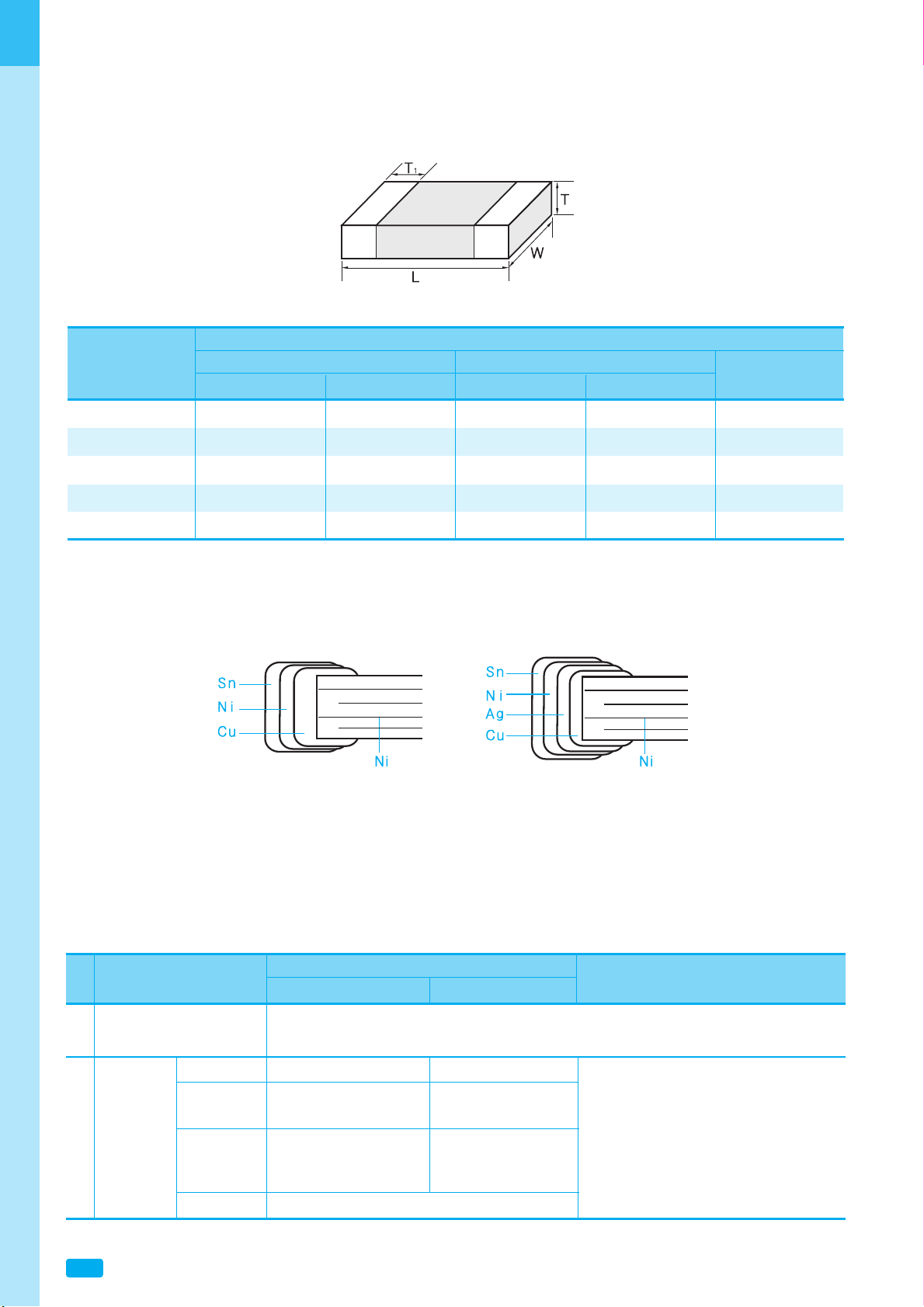
Dimensions
Code Length Width
L Tol(±) W Tol(±)
T1(min)
1005(0402) 1.00 0.05 0.50 0.05 0.05
1608(0603) 1.60 0.15 0.80 0.10 0.10
2012(0805) 2.00 0.20 1.25 0.15 0.10
3216(1206) 3.20 0.30 1.60 0.20 0.15
3225(1210) 3.20 0.40 2.50 0.25 0.15
Dimensions
Construction of Termination
a. Ni TypeⅠ b. Ni TypeⅡ (Soft Termination)
1. Pre-and Post-Stress
Electrical Test
2. High
Temperature
Exposure
(Storage)
Appearance
Capacitance
Change
Q/D.F.
I.R.
No marking defects
Within
±2.5% or ±0.25pF
(Whichever is larger)
30pF Min.: Q
≥
1000
30pF Max.: Q
≥
400+20×C
C: Nominal Capacitance(pF)
More than 10,000M
Ω
or 500
Ω.F
(Whichever is smaller)
Within
±10.0%
Rated Voltage
16V Min.: 0.05 Max.
10V: 0.075 Max.
Temperature : 150
±3℃
Maintenance Time : 1000+48/-0 hrs
Let sit for 24
±2 hours at room temperature,
then measure.
No.
AEC-Q200
Specification
Class
Ⅰ ClassⅡ
Test Methods and Conditions
Specifications and Test Methods (For Automotive Applications)
Page 26
Multi Layer Ceramic Capacitors
29
Automotive Applications
3. Temperature
Cycle
Appearance
Capacitance
Change
Q/D.F.
I.R.
No marking defects
Within
±2.5% or ±0.25pF
(Whichever is larger)
30pF Min.: Q
≥
1000
30pF Max.: Q
≥
400+20×C
C: Nominal Capacitance(pF)
More than 10,000M
Ω
or 500
Ω.F
(Whichever is smaller)
Within
±10.0%
Rated Voltage
16V Min.: 0.05 Max.
10V: 0.075 Max.
Within
±12.5%
Rated Voltage
16V Min.: 0.05 Max.
10V: 0.075 Max.
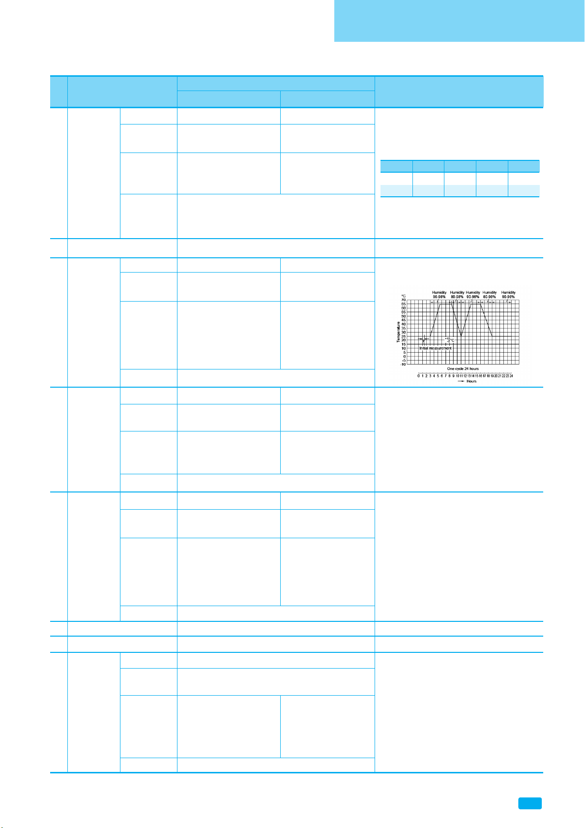
Perform the 1000 cycles according to the four
heat treatments listed in the following table.
Let sit for 24
±2 hours at room temperature,
then measure.
5. Moisture
Resistance
Appearance
Capacitance
Change
Q/D.F.
I.R.
No marking defects
Within
±3.0% or ±0.30pF
(Whichever is larger)
30pF Min.: Q
≥
350
10pF Min. and 30pF
Max.: Q
≥
275+5/2×C
10pF Max.: Q
≥
200+10×C
C: Nominal Capacitance(pF)
More than 10,000M
Ω
or 500
Ω.F
(Whichever is smaller)
Temperature : 25~65
℃
, Humidity : 80~98%
Cycle Time : 24 hrs/cycle, 10 cycles
Within
±12.5%
Rated Voltage
16V Min.: 0.05 Max.
10V: 0.075 Max.
6. Biased
Humidity
Appearance
Capacitance
Change
Q/D.F.
I.R.
No marking defects
Within
±3.0% or ±0.30pF
(Whichever is larger)
30pF Min.: Q
≥
200
30pF Max.: Q
≥
100+10/3×C
C: Nominal Capacitance(pF)
More than 10,000M
Ω
or 500
Ω.F
(Whichever is smaller)
Temperature : 85
±3
℃
Humidity : 80~85%
Applied Voltage : Rated Voltage and 1.3+0.2/-0V
Maintenance Time : 1000+48/-0 hrs
Let sit for 24
±2 hours at room temperature,
then measure.
The charge/discharge current is less than
50mA.
Rated Voltage
50V: 0.025 Max.
25V: 0.03 Max.
16V: 0.035 Max.
10V: 0.05 Max.
10. Resistance to
Solvents
Appearance
Capacitance
Change
Q/D.F.
I.R.
No marking defects
Within the specified tolerance
30pF Min.: Q
≥
1000
30pF Max.: Q
≥
400+20×C
C: Nominal Capacitance(pF)
More than 10,000M
Ω
or 500
Ω.F
(Whichever is smaller)
Per MIL-STD-202 Method 215
Within±12.5%
Rated Voltage
16V Min.: 0.05 Max.
10V: 0.075 Max.
7. Operational
Life
Appearance
Capacitance
Change
Q/D.F.
I.R.
No marking defects
Within
±3.0% or ±0.30pF
(Whichever is larger)
30pF Min.: Q
≥
350
10pF Min. and 30pF
Max.: Q
≥
275+5/2×C
10pF Max.: Q
≥
200+10×C
C: Nominal Capacitance(pF)
More than 10,000M
Ω
or 500
Ω.F
(Whichever is smaller)
Temperature : 125
±3
℃
Applied Voltage : Rated Voltage× 200%
Maintenance Time : 1000+48/-0 hrs
Let sit for 24
±2 hours at room temperature,
then measure. The charge/discharge current is
less than 50mA.
Initial Measurement for Class II
Applied 200% of the rated voltage for one hour
at 125
±3
℃
Remove and let sit for 24±2 hours at
room temperature, then measure.
8. External Visual
9. Physical Dimension
No defects or abnormalities
Within the specified dimensions
Visual inspection
Using calipers
4. Destructive Physical Analysis
No defects or abnormalities Per EIA-469
Initial measurement
Perform the initial measurement according to
Note 1 for Class II.
No.
AEC-Q200
Specification
Class
Ⅰ ClassⅡ
Test Methods and Conditions
Step 1 2 3 4
Temp.(
℃
) -55+0/-3 25±2 125+3/-0 25±2
Time(min) 15±3115±31
Page 27
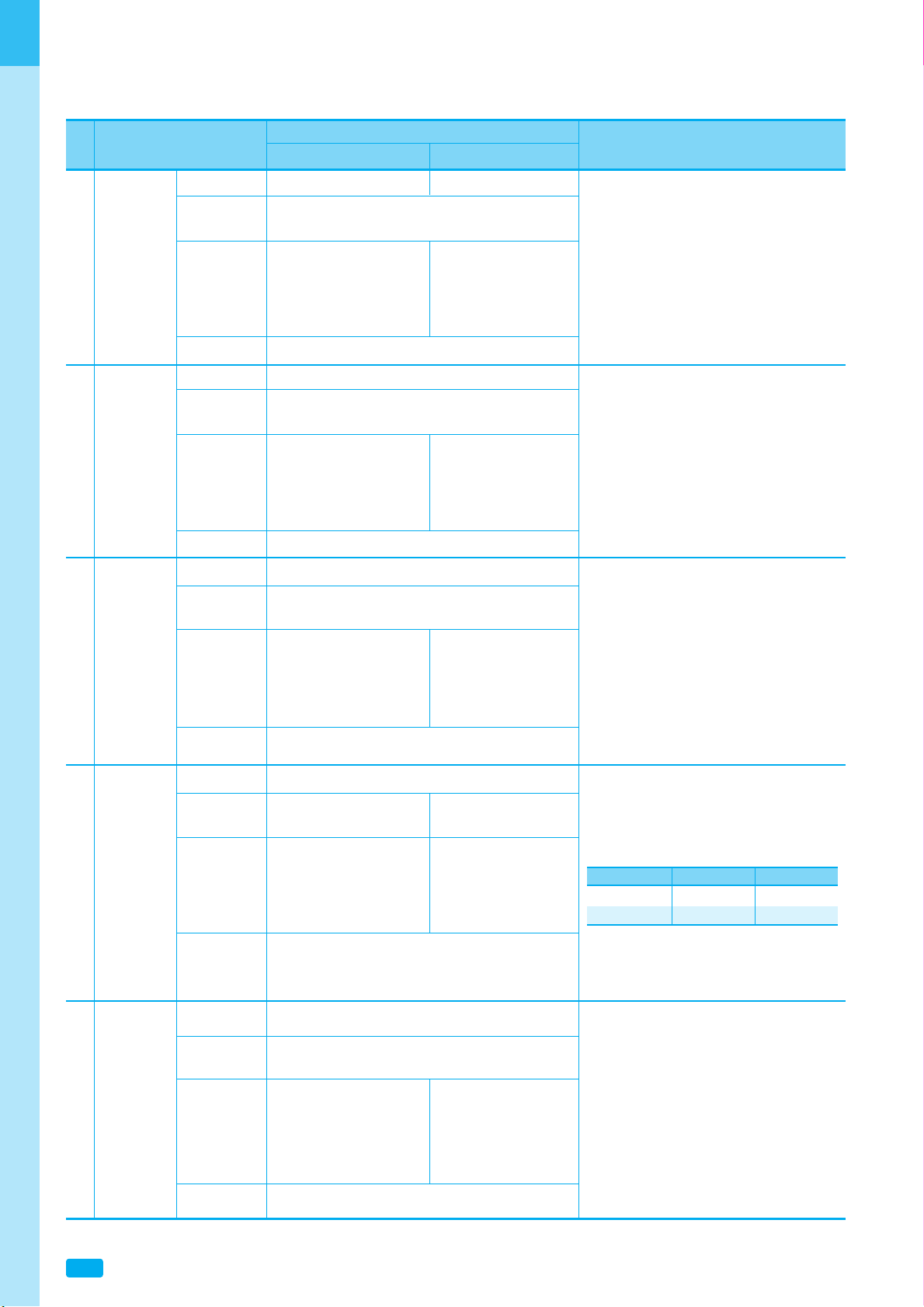
SAMWHA CAPACITOR Co., Ltd.
30
www.samwha.com
Multi Layer Ceramic Capacitors
Rated Voltage
50V: 0.025 Max.
25V: 0.03 Max.
16V: 0.035 Max.
10V: 0.05 Max.
11. Mechanical
Shock
Appearance
Capacitance
Change
Q/D.F.
I.R.
No marking defects
Within the specified tolerance
30pF Min.: Q
≥
1000
30pF Max.: Q
≥
400+20×C
C: Nominal Capacitance(pF)
More than 10,000M
Ω
or 500
Ω.F
(Whichever is smaller)
Three shocks in each direction should be
applied along 3 mutually perpendicular axes of
the test specimen (18 shocks)
Test Pulse
Wave form : Half-sine
Duration : 0.5ms
Peak value : 1,500G
Velocity change : 4.7m/s
Rated Voltage
50V: 0.025 Max.
25V: 0.03 Max.
16V: 0.035 Max.
10V: 0.05 Max.
12. Vibration
Appearance
Capacitance
Change
Q/D.F.
I.R.
No defects or abnormalities
Within the specified tolerance
30pF Min.: Q
≥
1000
30pF Max.: Q
≥
400+20×C
C: Nominal Capacitance(pF)
More than 10,000M
Ω
or 500
Ω.F
(Whichever is smaller)
The specimens should be subjected to a
simple harmonic motion having a total
amplitude of 1.5mm. The entire frequency
range of 10 to 2,000 Hz and return to 10 Hz
should be traversed in 20 minutes. This cycle
should be performed 12 times in each of three
mutually perpendicular directions (total of 36
times).
Rated Voltage
50V: 0.025 Max.
25V: 0.03 Max.
16V: 0.035 Max.
10V: 0.05 Max.
13. Resistance to
Soldering
Heat
Appearance
Capacitance
Change
Q/D.F.
I.R.
No marking defects
Within the specified tolerance
30pF Min.: Q
≥
1000
30pF Max.: Q
≥
400+20×C
C: Nominal Capacitance(pF)
More than 10,000MΩor 500
Ω.F
(Whichever is smaller)
Temperature (Eutectic solder solution) : 260
±5
℃
Dipping Time : 10±1s
Let sit for 24
±2 hours at room temperature,
then measure.
Initial measurement
Perform the initial measurement according to
Note 1 for Class II.
Rated Voltage
50V: 0.025 Max.
25V: 0.03 Max.
16V: 0.035 Max.
10V: 0.05 Max.
14. Thermal
Shock
Appearance
Capacitance
Change
Q/D.F.
I.R.
No marking defects
Within
±3.0% or ±0.30pF Within±12.5%
(Whichever is larger)
30pF Min.: Q
≥
1000
30pF Max.: Q
≥
400+20×C
C: Nominal Capacitance(pF)
More than 10,000M
Ω
or 500
Ω.F
(Whichever is smaller)
Perform the 300 cycles according to the two
heat treatments listed in the following table.
Transfer Time : 20s Max.
Let sit for 24
±2 hours at room temperature, then
measure.
Rated Voltage
50V: 0.025 Max.
25V: 0.03 Max.
16V: 0.035 Max.
10V: 0.05 Max.
15. ESD
Appearance
Capacitance
Change
Q/D.F.
I.R.
No marking defects
Within the specified tolerance
30pF Min.: Q
≥
1000
30pF Max.: Q
≥
400+20×C
C: Nominal Capacitance(pF)
More than 10,000M
Ω
or 500
Ω.F
(Whichever is smaller)
Per AEC-Q200-002
No.
AEC-Q200
Specification
Class
Ⅰ ClassⅡ
Test Methods and Conditions
Initial measurement
Perform the initial measurement according to
Note 1 for Class II.
Step 1 2
Temp.(
℃
) -55+0/-3 125+3/-0
Time(min) 15±315±3
Page 28
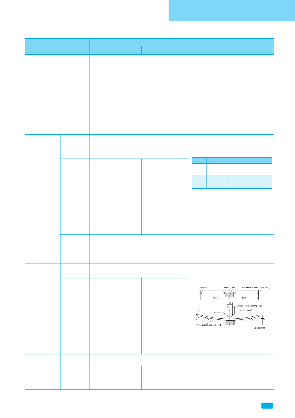
Multi Layer Ceramic Capacitors
31
Automotive Applications
16. Solderability
95% of the terminations is to be soldered evenly
and continuously.
(a) Preheat at 155℃for 4 hours, and then
immerse the capacitor in a solution of ethanol
and rosin. Immerse in eutectic solder solution
for 5+0/-0.5 seconds at 235
±5
℃.
(b) Steam aging for 8 hours, and then immerse
the capacitor in a solution of ethanol and rosin.
Immerse in eutectic solder solution for 5+0/-0.5
seconds at 235
±5
℃.
(c) Steam aging for 8 hours, and then immerse
the capacitor in a solution of ethanol and rosin.
Immerse in eutectic solder solution for 120
±5
seconds at 260
±5
℃.
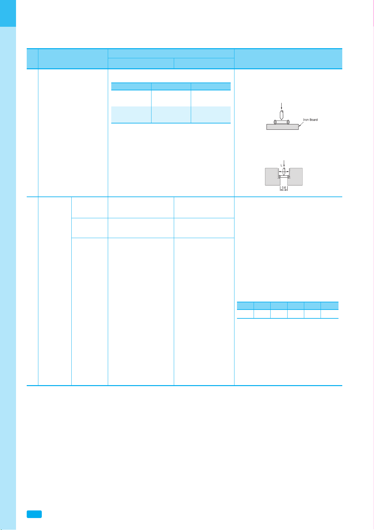
18. Board Flex
Appearance
Capacitance
Change
No marking defects
Within ±5.0% or ±0.5pF Within±10.0%
(Whichever is larger)
Apply a force in the direction shown in the
following figure for 5
±1 seconds.
19. Terminal
Strength
Appearance
Capacitance
Change
No marking defects
Within
±5.0% or ±0.5pF Within±10.0%
(Whichever is larger)
Apply *18N force in parallel with the test jig for
60
±1 seconds.
*10N for 1608(EIA:0603) size
2N for 1005(EIA:0402) size
Flexure for Class I:
≤3
mm
for Class II:
≤
2mm
Rated Voltage
50V: 0.025 Max.
25V: 0.03 Max.
16V: 0.035 Max.
10V: 0.05 Max.
More than 100,000M
Ω
or 500
Ω.F
(Whichever is smaller)
More than 10,000M
Ω
or 10
Ω.F
(Whichever is smaller)
17. Electrical
Characteriza
-tion
Appearance
Capacitance
Change
Q/D.F.
I.R. at 25
℃
I.R. at 125
℃
Dielectric
Strength
No defects or abnormalities
Within the specified tolerance
30pF Min.: Q
≥
1000
30pF Max.: Q
≥
400+20×C
C: Nominal Capacitance(pF)
More than 100,000M
Ω
or 1,000
Ω.F
(Whichever is smaller)
More than 10,000M
Ω
or 100
Ω.F
(Whichever is smaller)
No dielectric breakdown or mechanical breakdown
The capacitance/Q/D.F. should be measured at
25
℃
at the frequency and voltage shown in the
table
Should be measured with a DC voltage not
exceeding rated voltage at 25
℃
and 125℃for 2
minutes of charging.
Applied 250% of the rated voltage for 1~5
seconds
The charge/discharge current is less than
50mA.
No.
AEC-Q200
Specification
Class
Ⅰ ClassⅡ
Test Methods and Conditions
Class Capacitance (C) Frequency Voltage
Class I C≤1000pF 1±0.1MHz 0.5~5Vrms
C>1000pF 1±0.1kHz 1±0.2Vrms
Class II C≤110μF1±0.1kHz 1±0.2Vrms
C>10μF 120±24Hz 0.5±0.1Vrms
Page 29
SAMWHA CAPACITOR Co., Ltd.
32
www.samwha.com
Multi Layer Ceramic Capacitors
20. Beam Load Test
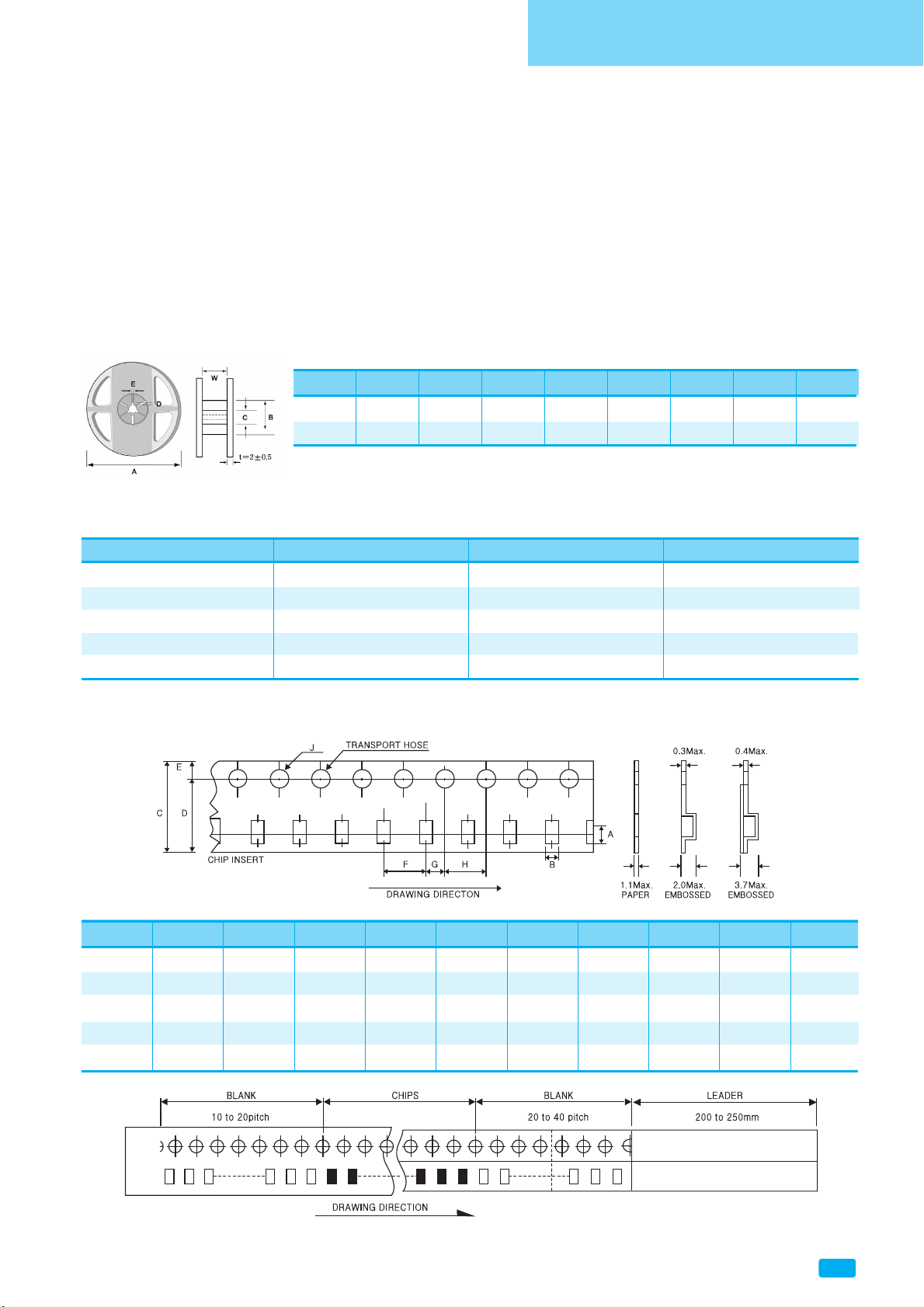
The chip endure following force. Apply a force as shown in the following figure.
(i) Chip Length : 2.5mm Max.
Beam Speed : 0.5mm/s
No.
AEC-Q200
Specification
Class
Ⅰ ClassⅡ
Test Methods and Conditions
Chip Length Thickness (T) Force
2.5mm Max.
T≤0.5mm 8N
T>0.5mm 20N
3.2mm Min.
T<1.25mm 15N
T≥1.25 54.5N
(ii) Chip Length : 3.2mm Min.
Beam Speed : 2.5mm/s
Within±15%
21. Capacitance
Temperature
Characteristics
Capacitance
Change
Temperature
Coefficient
Capacitance
Drift
0
±30 ppm/
℃
Within ±0.2% or ±0.05pF
(Whichever is larger)
(i) Class I
The temperature coefficient is determined
using the capacitance measured in step 3 as a
reference. When cycling the temperature
sequentially from step 1 through 5, the
capacitance should be within the specified
tolerance for the temperature coefficient.
The capacitance drift is calculated by dividing
the differences
between the maximum and minimum
measured values in steps
1, 3 and 5 by the capacitance value in step 3.
(ii) Class II
The ranges of capacitance change compared
with the 25
℃
value over the temperature range
from -55
℃
to 125
℃
Initial measurement
Perform the initial measurement according to
Note 1 for Class II.
Step 1 2 3 4 5
Temp.(℃)
25±2 -55±325±2 125±325±2
*Note 1. Initial Measurement for Class II
Perform a heat treatment at 150+0/-10
℃
for one hour, and then let sit for 24±2 hours at room temperature, then measure.
Page 30
Multi Layer Ceramic Capacitors
33
Automotive Applications
Packing
Mark
Size Code EIA Code
AB CD E W
7" REEL 1005~3225 0402~1210 Ø178±2 Ø50Min. Ø13±0.5 Ø21±0.8 2±0.5 10±1.5
13" REEL 1005~3225 0402~1210 Ø330±2 Ø70Min. Ø13±0.5 Ø21±0.8 2±0.5 10±1.5
Type EIA CODE 7" Quantity(EA)/Reel 13" Quantity(EA)/Reel
1005 0402 10,000 50,000
1608 0603 4,000 16,000
2012 0805 3,000 ~ 4,000 10,000
3216 1206 2,000 ~ 4,000 6,000 ~ 10,000
3225 1210 1,000 ~ 3,000 4,000 ~ 10,000
TYPE
EIA CODE
AB CDEFGHJ
1005 0402 1.15
±0.1 0.65±0.1 8.0±0.3 3.5±0.05 1.75±0.1 2.0±0.05 2.0±0.1 4.0±0.1 1.5±0.1
1608 0603 1.9
±0.2 1.10±0.2 8.0±0.3 3.5±0.05 1.75±0.1 4.0±0.1 2.0±0.1 4.0±0.1 1.5±0.1
2012 0805 2.4±0.2 1.65±0.2 8.0±0.3 3.5±0.05 1.75±0.1 4.0±0.1 2.0±0.1 4.0±0.1 1.5±0.1
3216 1206 3.6±0.2 2.00±0.2 8.0±0.3 3.5±0.05 1.75±0.1 4.0±0.1 2.0±0.1 4.0±0.1 1.5±0.1
3225 1210 3.6±0.2 2.80±0.2 8.0±0.3 3.5±0.05 1.75±0.1 4.0±0.1 2.0±0.1 4.0±0.1 1.5±0.1
Number of Packages
Tape Dimensions
Bulk packing
① 1000 pcs per Polybag
② 5 Polybags per Inner box
③ 10 Inner boxes per Out box
Reel Dimensions
Reel Packing
① 8~10 Reels per Inner box
② 10 Inner boxes per Out box
Page 31
SAMWHA CAPACITOR Co., Ltd.
34
www.samwha.com
Multi Layer Ceramic Capacitors
Size Code
(EIA Code)
Cap.
0.5㎊(0R5)
1㎊(010)
2㎊(020)
3㎊(030)
4㎊(040)
5㎊(050)
6㎊(060)
7㎊(070)
8㎊(080)
9㎊(090)
10㎊(100)
12㎊(120)
15㎊(150)
18㎊(180)
22㎊(220)
27㎊(270)
33㎊(330)
39㎊(390)
47㎊(470)
56㎊(560)
68㎊(680)
82㎊(820)
100㎊(101)
120㎊(121)
150㎊(151)
180㎊(181)
220㎊(221)
270㎊(271)
330㎊(331)
390㎊(391)
470㎊(471)
560㎊(561)
680㎊(681)
820㎊(821)
1000㎊(102)
1200㎊(122)
1500㎊(152)
1800㎊(182)
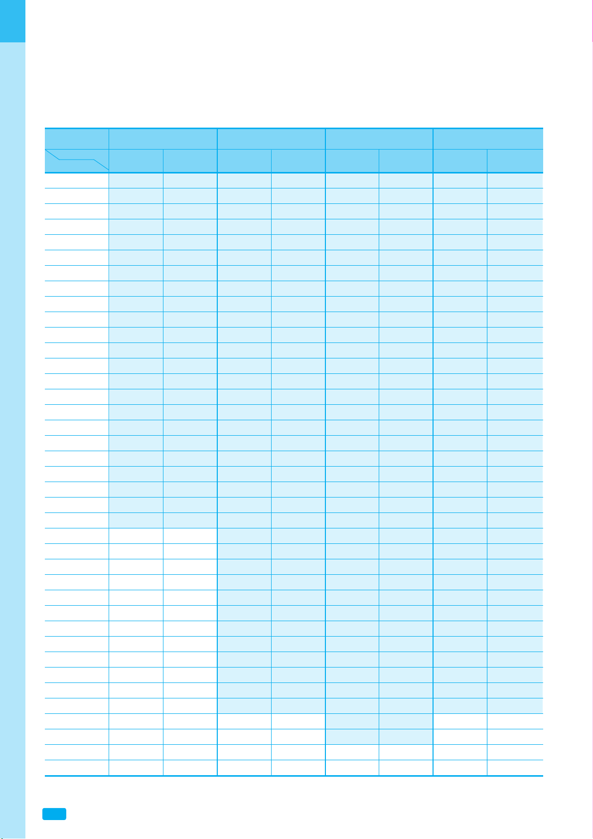
2200㎊(222)
Class I (C0G)
Capacitance Table.
Volt(V)
1005(0402)
2525 50 25 50 25 50 50 100
1608(0603) 2012(0805) 3216(1206)
Page 32
Multi Layer Ceramic Capacitors
35
Automotive Applications
Size Code
(EIA Code)
Cap.
1000㎊(102)
1500㎊(152)
2200㎊(222)
3300㎊(332)
4700㎊(472)
6800㎊(682)
10000㎊(103)
15000㎊(153)
22000㎊(223)
33000㎊(333)
47000㎊(473)
68000㎊(683)
0.1㎌(104)
0.15㎌(154)
0.22㎌(224)
0.33㎌(334)
0.47㎌(474)
0.68㎌(684)
1.0㎌(105)
2.2㎌(225)
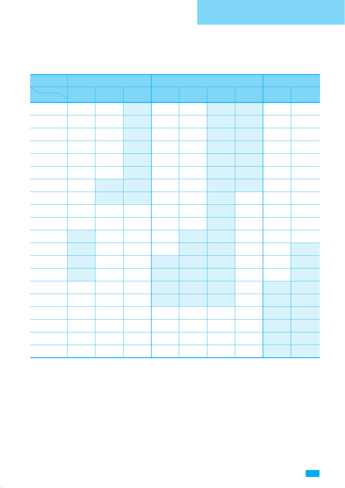
Class II (X7R)
Volt(V)
1608(0603)
16 25 50 16 25 50 100 25 50
2012(0805) 3216(1206)
Page 33
www.samwha.com
Multi Layer Ceramic Capacitors
SAMWHA CAPACITOR Co., Ltd.
36
Caution
▶ Storage Condition
When solderability is considered, capacitor are recommended to be used in 12 months.
(1) Temperature: 25
℃
± 10
℃
(2) Relative Humidity: Below 70% RH
▶ The Regulation of Environmental Pollution Materials
Never use materials mentioned below in MLCC products regulated this document.
Pb, Cd, Hg, Cr+6, PBB(Polybrominated biphenyl), PBDE(Polybrominated diphenyl ethers), asbestos
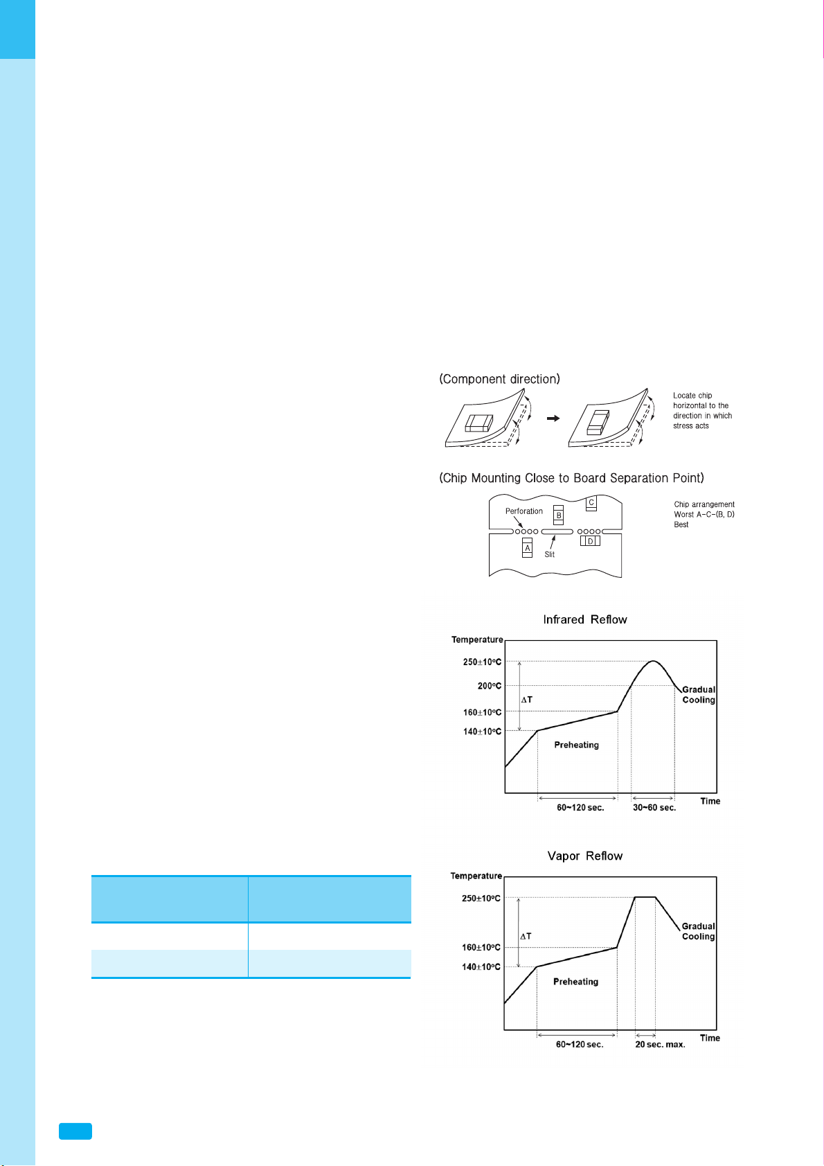
▶ Mounting Position
Choose a mounting position that minimizes the stress
imposed on the chip during flexing or bending of the
board.
▶ Reflow Soldering
1. The sudden temperature change easily causes
mechanical damages to ceramic components.
Therefore, the preheating procedures should be
required for the soldering of ceramic components.
2. Please refer to the recommended soldering profiles as
shown in figures, and keep the temperature
difference(△T) within the range recommended in
Table 1.
Table 1.
Size code Temperature
(EIA Code) Difference
1005~3216 (0402~1206) △T≤190℃
3225 (1210) △T≤130℃
Page 34
Multi Layer Ceramic Capacitors
37
Automotive Applications
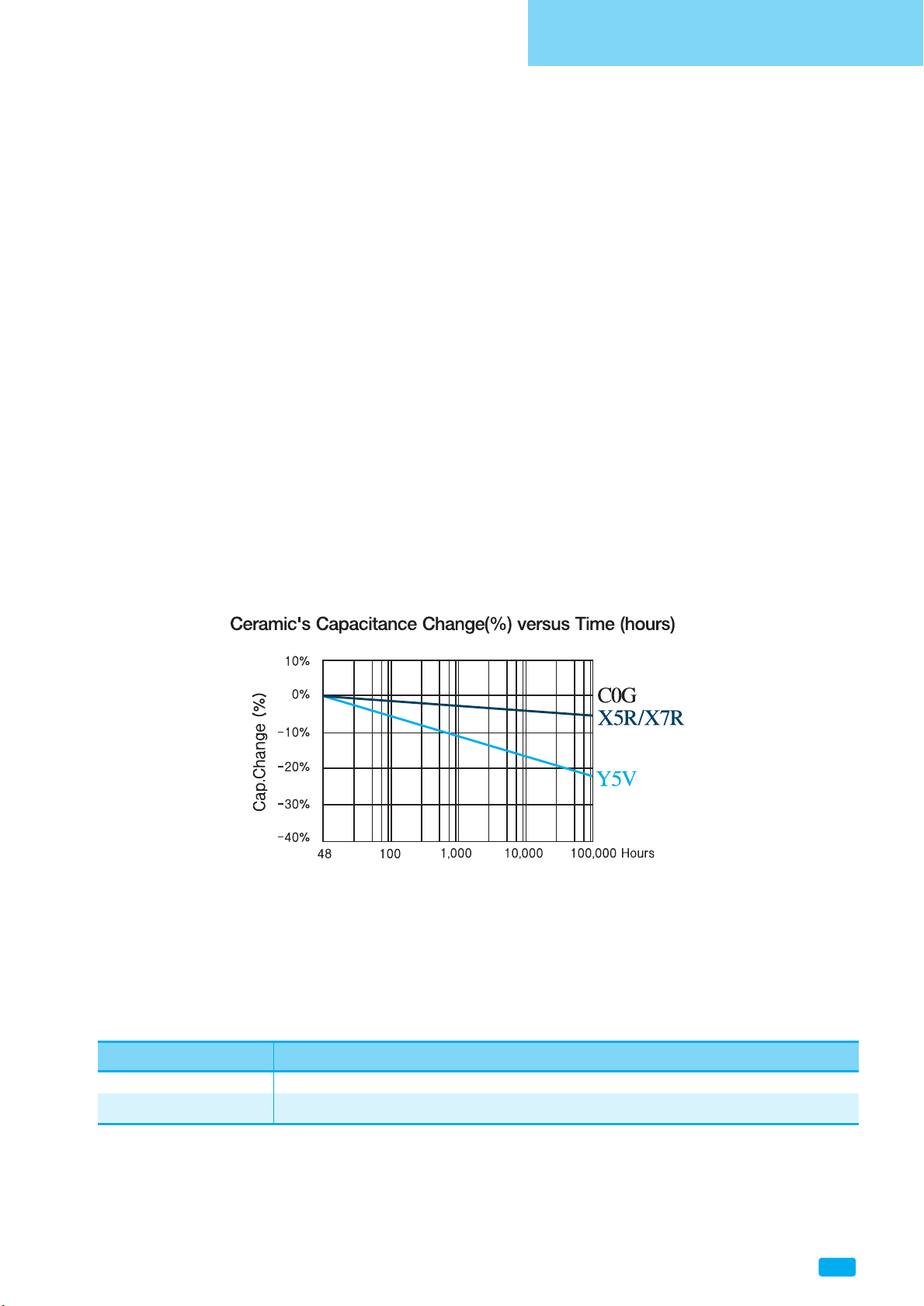
▶ 'Aging'/'De-aging' behavior of high dielectric constant type MLCCs
(Typically represented by X7R temperature characteristic of which main composition is BaTiO3)
'Aging' / 'De-aging' Behavior of high dielectric MLCCs Please note that high dielectric type dielectric ceramic
capacitors have a "normal" 'aging' behavior / characteristic, that is; their capacitance value decreases with time
from its value when it was first manufactured. From that date, the capacitance value begins to decrease at a
logarithmic rate defined by:
Ct= C48(1 - k log10 t)
The capacitance value can be restored (also known as 'de-aged') by exposing the component to elevated
temperatures approaching its curie temperature (approximately 120℃). This 'de-aging' can occur during the
component's solder-assembly onto the PCB, during life or temperature cycle testing, or by baking at 150℃
for about 1 hour.
Ct: Capacitance value, t hours after the start of 'aging'
C48: Capacitance value, 48 hours after its manufacture
k : Aging constant (capacitance decrease per decade-hour)
t : time, in hours, from the start of 'aging'
Dielectric Maximum percent capacitance loss per decade hour, k
C0G 0
X7R ~3%
 Loading...