

Datasheet MU9C4K64-90TDC, MU9C4K64-90TDI, MU9C4K64-70TDC, MU9C4K64-12TDI, MU9C4K64-35TDC Datasheet (MUSIC)
...Page 1
Data Sheet
MUSIC Semiconductors, the MUSIC logo, and the phrase “MUSIC Semiconductors” are
June 1 2002 Rev. 6
Registered trademarks of MUSIC Semiconductors. MUSIC is a trademark of
MUSIC Semiconductors.
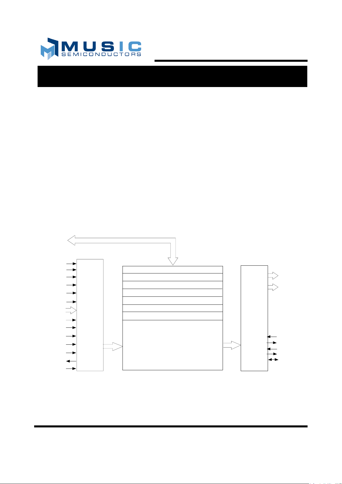
DQ31–0
/VB
AA Bus
PA3–0
/MM
/RESET
TCLK
TMS
TDI
TDO
/TRST
CONTROL
AND
ADDRESS
DECODER
PRIORITY
ENCODER
AND
FLAG
LOGIC
/E
/CS1
/CS2
/W
/OE
/AV
AC Bus
/DSC
INSTRUCTION REGISTER
DEVICE SELECT REGISTER
STATUS REGISTER
CONFIGURATION REGISTER
ADDRESS REGISTER
MASK REGISTERS 1–7
COMPARAND REGISTER
4 K x 64 Word
(MU9C4K64)
8 K x 64 Word
(MU9C8K64)
Address Database
/M F
/M I
/FF
/FI
Figure 1: Block Diagram
APPLICATION BENEFITS
• 28 million IPv4 packets per second supports up to 18
Gb Ethernet or 7 OC-48 ATM ports at wire speed
• Exact match on MAC addresses
• Processes DA and SA within 190 ns, supporting three ports
of 1 Gb or 34 ports of 100 Mb Ethernet at wire
speed
• Mixed mode L3 and L2 single search engine for two ports
at 1 Gb or 29 ports of 100 Mb Ethernet at wire
speed
• Directly addresses external RAM containing
associated data of any width
• Hardware control states directly address memory and
registers; Instruction and Status registers for optional
software control
DISTINCTIVE CHARACTERISTICS
• 4K and 8K x 64-bit words
• 64-bit binary compares
• 35 ns deterministic compare and output time
• 32-bit Data I/O port
• 16-bit Match Address Output port
• Address/Control bus directly controls device operations for
faster operation or higher throughput
• Seven selectable mask registers
• Synchronous operation
• Cascadable for increased depth
• Extensive set of control states for flexibility
• JTAG interface
• 100-pin LQFP package; 3.3 Volt operation
MU9C Routing Coprocessor (RCP) Family
Page 2
MU9C Binary Routing Coprocessor (RCP) Family General Description
2
Rev. 6
GENERAL DESCRIPTION
The MU9C RCP family consists of 4K and 8K x 64-bit
Routing Coprocessors (RCPs) with a 32-bit wide data
interface. The device is designed for use in layer 2
switches to provide very high throughput address
translation using tables held in external RAM. The MU9C
RCP has a fully deterministic search time, independent of
the size of the list and the position of the data in the list.
This unique feature guarantees that the wire speed address
recognition does not impact the latency or induce some
jitter on the latency of the global system. Address fields
from the packet header are compared against a list of
entries stored in the array. As a result of the comparison,
the MU9C RCP generates an index that is used to access
an external RAM where port mapping data and other
associated information is stored.
A set of control states provides a powerful and flexible
control interface to the MU9C RCP. This control structure
allows memory read and write, register read and write,
data move, comparison, validity control, addressing
control, and initialization operations.
The MU9C RCP architecture uses direct hardware control
of the device and an independent bus for returning match
results. Software control is also supported for systems
where maximum performance is not needed.
OPERATIONAL OVERVIEW
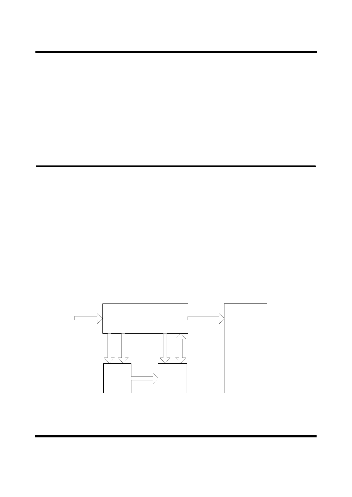
The MU9C RCP is designed to act as an address translator
for lookup tables in layer 2 switches. Refer to Figure 2 for
a simplified block diagram of a switch. During normal
operation, the controller extracts the address information
from an arriving packet to form the comparand, which is
then compared against the contents of the MU9C RCP.
The MU9C RCP generates an index that is used to access
the data in an external RAM, which holds the destination
port for accessing the network. The controller reads the
data from the RAM and forwards the packet.
The validity of a location in the Address Database is
determined by an extra bit called the Validity bit. This bit is
set and reset either with an index or an associative match.
Therefore, when a new entry is written to the database, its
Validity bit is set valid.
The index at which a write takes
place is driven onto the PA:AA bus, so that output port
data can be written simultaneously into the external RAM
at the correct index.
When a database location is deleted, the Validity bit for that
entry is reset, and the index of the location is driven onto
the Active Address bus. This simple mechanism allows
easy maintenance of the tables in both the database and the
external RAM.
The MU9C RCP supports simple daisy chained vertical
cascading that serves to prioritize multiple devices and
provides system-level match and full indication. If the
slight timing overhead associated with the daisy chain is
unacceptable, the MU9C RCP is designed to facilitate
external prioritization across multiple devices.
Figure 2: Switch Block Diagram
Controller
RAM
Switch
Fabric
MU9C
Switch Control
and Packet Data
Network
Address
Data
RCP
Control
Packet Stream
RAM
Address
Page 3
Pin Descriptions MU9C Binary Routing Coprocessor (RCP) Family
Rev. 6 3
PIN DESCRIPTIONS
Note: Signal names that start with a slash (“/”) are active LOW.
All signals are 3.3V CMOS level. Never leave inputs floating.
The CAM architecture draws large currents during compare
operations, mandating the use of good layout and bypassing
techniques. Refer to the Electrical Characteristics section for
more information.
DQ31–0 (Data Bus, Three-state, Common Input/
Output)
The DQ31–0 lines convey data to and from the MU9C
RCP. When the /E input is HIGH the DQ31–0 lines are
held in their high-impedance state. The /W input
determines whether data flows to or from the device on the
DQ31–0 lines. The source or destination of the data is
determined by the AC bus, DSC, and the /AV line. During
a Write cycle, data on the DQ31–0 lines is registered by
the falling edge of /E.
AC12–0/AC11–0 (Address/Control Bus, Input)
When Hardware control is selected, the AC bus conveys
address or control information to the MU9C RCP,
depending on the state of the /AV input. When /AV is
LOW then the AC bus carries an address; when /AV is
HIGH the AC bus carries control information. Data on the
AC bus is registered by the falling edge of /E. When
software control is selected, the state of the AC bus does
not affect the operation of the device.
DSC (Data Segment Control, Input)
When DQ bus access to a 64 bit register or memory word
is performed, the DSC input determines whether bits 31–0
(DSC LOW) or bits 63–32 (DSC HIGH) are accessed.
Access to 32 bit registers require that DSC be held LOW.
AA12–0/AA11–0 (Active Address, Output)
The AA bus conveys the Match address, the Next Free
address, or Random Access address, depending on the
most recent memory cycle. The /OE input enables the AA
bus; when the /OE input is HIGH, the AA bus is in its
high-impedance state; when /OE is LOW the AA bus is
active. In a vertically cascaded system after a Comparison
cycle, Write at Next Free Address cycle or Read/Write at
Highest-Priority match, only the highest-priority device
will enable its AA bus, regardless of the state of the /OE
input. In the event of a mismatch in the Address Database
after a Compare cycle, or after a Write at Next Free
Address cycle into an already full system, the
lowest-priority device will drive the AA bus with all 1s.
The AA bus is latched when /E is LOW, and are free to
change only when /E is HIGH.
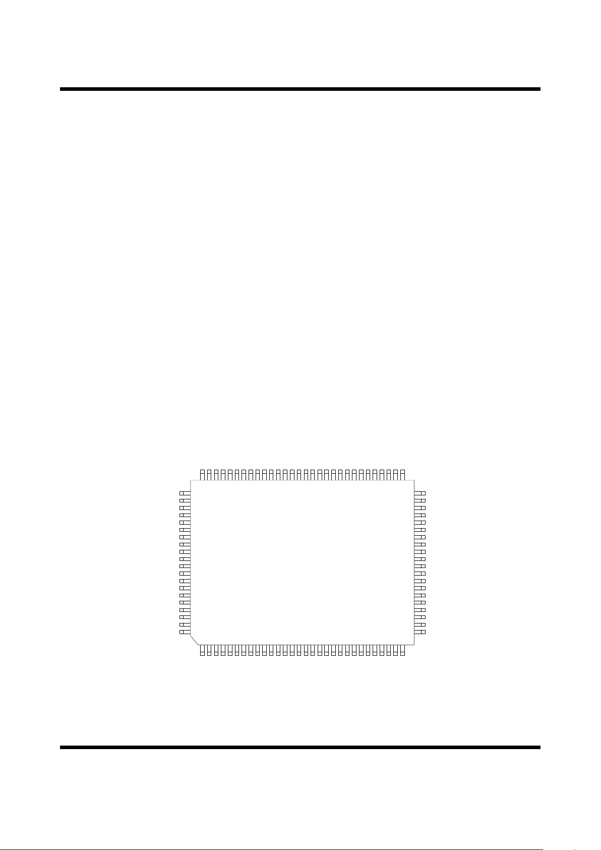
Figure 3: MU9C RCP Pinout
82
83
84
85
86
87
88
89
90
91
92
93
94
95
96
97
98
81
31
10 0
99
33
34
35
36
37
38
39
40
41
42
43
44
45
46
47
48
49
50
32
TCLK
TMS
TDI
DQ0
DQ1
DQ2
DQ3
VDD
DQ4
DQ5
DQ6
DQ7
VSS
DQ8
DQ9
DQ10
DQ11
VDD
DQ12
DQ13
DQ14
DQ15
VSS
VSS
VSS
AC11
AC10
AC9
AC8
AC7
AC6
VDD
AC5
AC4
AC3
AC2
AC1
AC0
TDO
AA12/NC*
8
0
7
9
7
8
7
7
7
6
7
5
7
4
7
3
7
2
7
1
7
0
6
9
6
8
6
7
6
6
6
5
6
4
6
3
6
2
6
1
6
0
5
9
5
8
5
7
5
6
5
5
5
4
5
3
5
2
5
1
D
Q
1
6
D
Q
1
7
D
Q
1
8
D
Q
1
9
V
D
D
D
Q
2
0
D
Q
2
1
D
Q
2
2
D
Q
2
3
V
S
S
D
Q
2
4
D
Q
2
5
D
Q
2
6
D
Q
2
7
V
D
D
D
Q
2
8
D
Q
2
9
D
Q
3
0
D
Q
3
1
V
S
S
/
E
/
W
/
C
S
1
/
C
S
2
/
O
E
V
S
S
/
A
V
/
V
B
/
R
E
S
E
T
/
T
R
S
T
1
2
3
4
5
6
7
8
9
1
0
1
1
1
2
1
3
1
4
1
5
1
6
1
7
1
8
1
9
2
0
2
1
2
2
2
3
2
4
2
5
2
6
2
7
2
8
2
9
3
0
V
S
S
V
S
S
A
A
1
2
/
N
C
*
A
A
8
V
S
S
A
A
7
A
A
6
A
A
5
A
A
4
V
D
D
A
A
3
A
A
2
A
A
1
A
A
0
V
S
S
/
M
F
/
F
F
V
D
D
/
M
I
/
F
I
V
S
S
/
M
M
D
S
C
P
A
3
P
A
2
P
A
1
P
A
0
A
A
1
0
A
A
9
A
A
1
1
MU9CxK64
100-Pin LQFP
(Top View)
* NC on MU9C4K64
Page 4

MU9C Binary Routing Coprocessor (RCP) Family Pin Descriptions
4
Rev. 6
PA3–0 (Page Address, Output)
The PA3–0 lines convey Page Address information. When
the /OE input is HIGH, the PA3–0 outputs are in their
high-impedance state; when /OE is LOW the PA3–0 lines
carry the Page Address value held in the Configuration
register. The PA3–0 lines are latched when /E is LOW, and
are free to change only when /E is HIGH. The Page
Address value of the currently active or highest-priority
responding device is output at the same time, and under
the same conditions, as the AA bus is active.
/E (Chip Enable, Input)
The /E input is the main chip enable and synchronizing
control for the MU9C RCP. When /E is HIGH, the chip is
disabled and the DQ31–0 lines are held in their
high-impedance state. The falling edge of /E registers the
/W, /CS1, /CS2, /AV, /AC bus, DSC, and the /VB and
DQ31–0 lines for a Write cycle. /E being LOW causes the
results of the previous comparison or memory access to be
latched on the PA:AA bus; when /E goes HIGH the latches
opens allowing the new comparison results or random
access memory address to flow to the PA:AA bus.
/CS1, /CS2 (Chip Select 1, Chip Select 2, Inputs)
The /CS1 and /CS2 inputs enable the MU9C RCP. If
either /CS1 or /CS2 are LOW, the device is selected for a
Read, Write, or Compare cycle through the DQ31–0 lines,
or for an internal data transfer. The /CS1 and /CS2 lines do
not have any effect on the PA:AA bus. The state of the
/CS1 and /CS2 lines is registered by the falling edge of /E.
/W (Write Enable, Input)
The /W input determines the direction of data transfer on
the DQ31–0 lines during Read, Write, and Data Move
cycles. When /W is LOW, data flows into the DQ31–0
lines; when /W is HIGH, data flows out. The /W line also
conditions the control state present on the AC bus and
DSC lines. The state of the /W line is registered by the
falling edge of /E.
/OE (Output Enable, Input)
The /OE input enables the PA:AA bus. When /OE is
HIGH, PA:AA bus are in their high-impedance state.
When /OE is LOW, PA:AA bus are active, and convey the
results of the last Comparison Cycle Match address or
Memory Access address. In a vertically cascaded system,
only the PA:AA bus of the highest-priority device will be
activated by /OE being LOW; in lower-priority devices,
the PA:AA bus remains in high-impedance regardless of
the state of /OE.
/AV (Address Valid, Input)
When Hardware control is selected, the /AV input
determines whether the AC bus carries address or control
information. When /AV is LOW, the AC bus conveys a
memory address; when /AV is HIGH, the AC bus conveys
control information. The state of the /AV line is registered
by the falling edge of /E. When software control is
selected, the /AV line distinguishes between instructions
and data on the DQ31–0 lines; when /AV is LOW, data is
present on the DQ31–0 lines; when /AV is HIGH, an
instruction is present on the DQ11–0 lines.
/VB (Validity Bit, Three-state, Common
Input/Output)
During accesses over the DQ31–0 lines, the /VB line
conveys validity information to and from the MU9C RCP.
During a Write cycle (/W=LOW), when /VB is LOW the
addressed location is set valid; when /VB is HIGH it is set
empty. During a Read cycle (/W=HIGH), the validity of
the addressed location is read on the /VB line. During a
Write cycle, the state of the /VB line is registered by the
falling edge of /E.
/MF (Match Flag, Output)
The /MF output indicates whether a valid match has
occurred during the previous Comparison cycle. If the /MF
output is HIGH at the end of a Comparison cycle, then no
match occurred; if it is LOW then either a match occurred
within the device, or the /MI input is LOW, conditioned by
the /MF output from a higher-priority device in the system.
The state of the /MF line will not change until after the
rising edge of /E during the Comparison cycle. Note that
/MF indicates the results of the most recent Comparison
cycle; it will not change when the PA:AA bus carry an
address other than the Match address.
/MI (Match Input, Input)
The /MI input receives match information from the next
higher-priority MU9C RCP in a vertically cascaded
system to provide system-level prioritization. When the
/MI input is HIGH, the /MF output will only go LOW if
there is a match during a Comparison cycle; when the /MI
input is LOW, the /MF output will go LOW. The /MF
output from one device is connected to the /MI input of the
next lower-priority device. The /MI pin of the
highest-priority device must be tied HIGH.
/FF (Full Flag, Output)
The /FF output indicates when all the memory locations
have their Validity bits set valid (LOW). When there is at
least one location with its Validity bit set HIGH, the /FF
output will be HIGH; when all locations have their Validity
bits set LOW, and the /FI input is LOW, the /FF output will
Page 5

MU9C Binary Routing Coprocessor (RCP) Family
Rev. 6 5
be LOW. If the /FI input is HIGH, the /FF output will be
HIGH. The state of the /FF line will not change until after
the rising edge of /E during a Write cycle.
/FI (Full Input, Input)
The /FI input receives full information from the next
higher-priority MU9C RCP in a vertically cascaded
system to provide system-level full information. When the
/FI input is LOW the /FF output will be HIGH if there is at
least one location whose Validity bit is set invalid; when
all locations have their Validity bits set valid, the /FF
output goes LOW. When the /FI input is HIGH, the /FF
output will remain HIGH. The /FF output from one device
is connected to the /FI input of the next lower-priority
device to give system-full indication. The /FI pin of the
highest-priority device must be tied LOW.
/MM (Multiple Match, Open Drain Output)
The /MM line indicates that there is a multiple match
within the system. When the /MI input is HIGH, the /MM
line is pulled LOW if there are at least two matches within
the MU9C RCP as a result of the previous Comparison
cycle; when there are less than two matches, the /MM line
floats HIGH. When the /MI input is LOW, the /MM line is
pulled LOW if there are one or more matches within the
MU9C RCP as a result of the previous Comparison cycle;
when there are no matches, the /MM line floats HIGH.
The /MM lines have open-drain outputs, so all /MM lines
within the system are connected together to give
system-level multiple match indication. The state of the
/MM line will not change until after the rising edge of /E
during a Comparison cycle.
/RESET
The /RESET input is used to reset the MU9C RCP to a
known state. When the /RESET line is pulled LOW it
causes the MU9C RCP to enter its reset state. After power
is applied to the MU9C RCP, the /RESET line must be
held LOW for a time equal to or greater than the minimum
RESET pulse width before the device can operate
correctly. This pin is internally pulled up.
TCLK (JTAG Test Clock, Input)
The TCLK input is the Test Clock input. This pin is
internally pulled up.
TMS (JTAG Test Mode Select, Input)
The TMS input is the Test Mode Select input. This pin is
internally pulled up.
TDI (JTAG Test Data Input, Input)
The TDI input is the Test Data input. This pin is internally
pulled up.
TDO (JTAG Test Data Output, Output)
The TCLK output is the Test Data Output. This pin is
internally pulled up.
/TRST (JTAG Reset, Input)
The /TRST input is the Reset input, and serves to reset the
Test Access Port circuitry to its reset condition. This pin is
internally pulled up.
VDD, VSS (Positive Power Supply, Ground)
These pins are the main power supply connections to the
MU9C RCP. VDD must be held at +3.3 Volts and ± 0.3
Volts relative to the VSS pin, which is at 0 Volts, system
reference potential, for correct operation of the device.
Note: The TCLK, TMS, TDI, TDO, and /TRST lines are defined
in the IEEE Standard Test Access Port and Boundary-scan
Architecture IEEE Standard. 1149.1-1990 and IEEE Standard.
1149.1a-1993.
FUNCTIONAL DESCRIPTION
Data is read from and written to the MU9C RCP through
the DQ31–0 lines. The Control bus, which is comprised of
Chip Enable (/E), two Chip Selects (/CS1, /CS2), Write
Enable (/W), Output Enable (/OE), Validity Bit Control
(/VB), Address Valid (/AV), Data Segment Control (DSC),
and the Address/Control inputs (AC bus) controls the
MU9C RCP. When the /AV line is LOW, the AC bus
carries an address for random access into the Memory
array; when it is HIGH, the AC bus conveys control
information. The MU9C RCP control states perform
Register Read/Write, Memory Read/Write, Data Move,
Comparison, Validity Bit Control, Initialization, and
Address Register Control. These functions are
summarized in Control State Overview on page 15.
Random access to memory locations occurs when the /AV
line is LOW; during a Write cycle, the validity of the
location is set by the /VB input. When the /AV line is
HIGH the control states allow read and write access to the
register set comprising Comparand register, seven mask
registers, a Configuration register, a Status register, an
Address register, a Device Select register, and an
Instruction register. The Configuration register sets the
persistent operating conditions of the device: the Page
address of the device, selection of mask register for
directly addressed memory writes, and selection between
hardware and software control.
Page 6

MU9C Binary Routing Coprocessor (RCP) Family Functional Description
6
Rev. 6
When Hardware control is selected, control is through the
AC bus and DSC line. When Software control is selected,
control is through the Instruction register, which is loaded
from the DQ bus. Under software control the /AV line is
used to distinguish between data and an instruction on the
DQ bus. Therefore, in Software Control mode, random
access to the Memory array can take place only using
indirect addressing through the Address register.
The two Chip Select lines /CS1, /CS2 enable the device and
simplify access to a multi-chip system, if either Chip Select
line is LOW the device is selected. The MU9C RCP also
can be selected through the Device Select register when its
value is set to that of the Page address of the device, and the
enable bit in the Device Select register is set LOW. The /OE
input enables the output signal and is used to synchronize
devices in a multi-chip system, and to prevent race
conditions among devices during priority resolution.
The output signals comprise the Active address (AA bus),
and the Page address (PA bus). The PA:AA bus provides
the current Active address, which is either the Match
address, Next Free address, or the Random Access
address, concatenated with the Device Page address. The
source of Active address is dependent on the previous
control state, allowing access to associated data in the
external RAM at the same location as an access in the
MU9C RCP for all types of cycles.
The Output enable, /OE, controls the PA:AA bus: when it is
LOW after a Compare cycle, the highest-priority
responding device outputs its Page and Match addresses on
PA:AA bus. Only the highest-priority responding device is
enabled, all other lower-priority devices will have their
PA:AA bus in the high-impedance state, regardless of the
state of their respective /OE lines: when /OE is HIGH, the
PA:AA remain in the high-impedance state.
When a mismatch occurs in the system, the lowest-priority
device, as defined in the Configuration register, will drive
the PA:AA bus with all 1s. When any Read or Write cycle
occurs, the address of the accessed location is output on
the PA:AA bus. The address output on the PA:AA bus is
persistent, and is held latched until /E goes HIGH during
the next cycle that changes the Active address. The PA:AA
bus is free to change only while /E is HIGH. Once /E goes
LOW, the state of the PA:AA bus is latched.
After a Compare cycle, the /MF and /MM flags are free to
change after /E has gone HIGH. Once the Match Flag
daisy chain has resolved device prioritization, the /OE
lines can be asserted to enable the PA:AA bus from the
highest-priority matching device.
In a multi-chip system, when a device remains deselected
during a Compare cycle through /CS1 and /CS2 being
HIGH and there being no match between the Device
Select register and the Page Address register, that device
will clear any previous positive match results. In other
words, if it had previously been indicating a match from
an earlier Comparison cycle, it will now be set to indicate
a mismatch, even though it was not selected during the
most recent Compare cycle.
For pure software control of the MU9C RCP, instructions
can be loaded into the Instruction register, and results read
from the Status register. The Status register holds the
results of comparison: PA:AA bus, /MF, /FF, and /MM
plus two PA:AA Validation bits that indicate the type of
cycle that generated the PA:AA bus value.
Vertical cascading is supported through a daisy chain
architecture. There are two daisy chains, one each for the
Match flag and the Full flag; the Multiple Match flag is
connected between devices through an open-drain line.
The Match flag (/MF) from a higher-priority device is
connected to the Match input (/MI) of the next
lower-priority device to provide prioritization throughout
a multiple device system. The /MF output from the
lowest-priority device provides a system Match flag. If the
delay through the daisy chain is unacceptable, the /OE
input can be used by external priority-resolution circuitry
to enable the highest-priority responder in the system.
The match conditions on the Match and Multiple Match
flag lines are persistent indicating the results of the most
recent Compare cycle. The Match flags are free to change
after the rising edge of /E during a Compare cycle, at
which time the daisy chain starts to resolve device
prioritization. Once the daisy chain has settled, the /OE
lines can be pulled LOW to access the Highest-Priority
Match address on the PA:AA bus.
The Multiple Match open-drain output (/MM) provides
multiple match indication when there are two or more
matches in a single device, or a device has its /MI input
LOW and has a match; the /MM flags of all devices in the
system are wire-ORed. Multiple responders can be
accessed sequentially by resetting the Highest-Priority
Match latch with the control state Advance to Next
Matching Location.
The Full flag (/FF) is cascaded from one device to the Full
Flag input (/FI) of the next lower-priority device in the
system. The /FF output from the lowest-priority device
provides a system Full flag. The Full flag is free to change
after the rising edge of /E during a Write cycle. The daisy
chains are persistent and are not conditioned by the /OE
input.
The MU9C RCP supports JTAG boundary-scan testing
through the pins TCK, TMS, TDI, TDO, and /TRST,
according to the IEEE 1149 Standard: Test Access Port
and Boundary-scan Architecture.
Page 7

Operational Characteristics MU9C Binary Routing Coprocessor (RCP) Family
Rev. 6 7
OPERATIONAL CHARACTERISTICS
Processor Interface
The processor interface is through a 32-bit data bus
DQ31–0 and control signals comprised of Chip Enable
(/E), two Chip Selects (/CS1, /CS2), Write Enable (/W),
Output Enable (/OE), Validity Bit Control (/VB), Address
Valid (/AV), Data Segment Control (DSC), and
Address/Control inputs (AC bus). When the /AV line is
LOW, the DSC and AC bus carries an address for random
access into the Memory array; when it is HIGH, the AC
bus conveys control information.
Most of the functionality of the MU9C RCP is accessed
through the control states on DSC and AC bus when /AV
is HIGH. The processor maps the control structure into
memory space and controls the MU9C RCP through
memory Read and Write cycles. Using this memory
mapping scheme, the /AV line should be driven from logic
that generates a HIGH level within the mapped range of
the control states, and a LOW level outside it. Other
control inputs /E, /W, /CS1, and /CS2 are analogous to
SRAM control inputs.
The /VB line acts like an extra data bit during memory
Read and Write cycles and is used to read and write the
validity of any memory location.
The MU9C RCP is enabled either through hardware
through /CS1 or /CS2 being LOW, or it is enabled by the
value written to the Device Select register matching with
the Page Address field of the Configuration register. One
extra bit in the Device Select register enables the
comparison between the Page Address value and the
Device Select register. These Chip Select mechanisms
operate in parallel. If any one is active, the device is
enabled.
The MU9C RCP can be controlled directly through
software. The Software Control mode is selected through
settings in the Configuration register.
When the Software Control mode is selected, control states
are written to the Instruction register from DQ11–0 during a
Write cycle with the /AV line held HIGH. DQ12 acts as the
DSC input. If the control state does not involve any data
transaction on the DQ31–0 lines, the instruction is executed
during the same cycle; the state of DQ13 modifies the
instruction, its state is equivalent to the /W input.
Note: It is up to the system designer to ensure that the correct
cycle type follows the loading of an instruction in Software
Control mode. If the instruction expects a Read cycle, and a
Write cycle is executed, or vice versa, the function of the MU9C
RCP is undefined. Such an error may lead to data loss, but will
not damage the device physically.
A Read cycle with the /AV line HIGH will access the
Status register, allowing results to be read back without
loading a new instruction. After a Comparison cycle,
Write at Next Free Address cycle or Read/Write at
Highest-Priority match in a vertically cascaded system,
only the highest-priority device will enable its DQ31–0
lines and output the contents of its Status register. After a
Comparison cycle, in the event of a mismatch in the
MU9C, the DQ31–0 lines of the lowest-priority device
will be enabled. After a random access Read or Write
cycle, the Status register of any selected device will be
enabled. Under these circumstances, it is up to the user to
ensure that only a single device is enabled through /CS1,
/CS2, or the Device Select register.
The instruction is persistent, so that all subsequent data
transactions will be executed according to the control state
held in the Instruction register. The results of a
Comparison cycle can be read back from the Status
register, and include PA:AA bus, /MF, /MM, and /FF. The
following sequence of events provides the fastest
operation of the MU9C RCP in Software Control mode:
Note: It is up to the system designer to ensure that the correct
cycle type follows the loading of an instruction in Software
Control mode. If the instruction expects a Read cycle, and a
Write cycle is executed, or vice versa, the function of the MU9C
RCP is undefined. Such an error may lead to data loss, but will
not damage the device physically.
Hardware Control
Direct hardware control using the AC bus and DSC line
enhances performance of the MU9C RCP. The AC bus
inputs determine which CAM location is accessed, and the
DSC determines whether bits 31–0 (DSC LOW) or bits
63–32 (DSC HIGH) are active. The Hardware Control
mode is selected when Configuration Register bits
FR27–26 are set LOW. The AC bus inputs are qualified by
/W, /AV, and /VB. When /AV is LOW, the AC bus and
DSC line carry the address for a random Read or Write
cycle, depending on the state of /W, and /VB carries the
validity of the location. During a Write cycle, /VB is
written to the Validity bit of the addressed location; during
a Read cycle, the validity of the location is read on the /VB
line. When /VB is LOW, the location contains valid data;
when /VB is HIGH the location is empty.
When /AV is HIGH, the AC bus and DSC line carry
address and control information. The DSC line selects
whether bits 31–0 (DSC LOW) or bits 63–32 (DSC
/AV Operation
1 Load ‘Compare DQ with CAM’ instruction
0 Comparand on DQ31–0
1 Read Status register
0 Next Comparand on DQ31–0
1 Read Status register, etc.
Page 8

MU9C Binary Routing Coprocessor (RCP) Family Operational Characteristics
8
Rev. 6
HIGH) participate in the operation. The AC8–6 lines
select the mask register and the AC5–0 lines provide the
Op-Code. If masking is not used, and all random
addressing of the memory is indirect through the Address
register, then only the DSC and AC5–0 lines are needed
for full control of the device.
In applications where a restricted number of control lines
are available, or where speed is not critical, the MU9C
RCP can be controlled in Software Control mode where
the control states are loaded into the Instruction register
through the DQ31–0 lines. The control states are identical
in both Hardware and Software Control modes, although
DQ12 and DQ13 take on special significance in Software
mode.
Software Control
For optimum performance, the AC bus and DSC line
control the MU9C RCP, allowing data transactions
through the DQ31–0 lines during a control cycle. In cases
where the overhead of a separate data load cycle can be
accommodated, the MU9C RCP can be operated through
the Instruction register. The AC bus and DSC line are not
used.
Control through the Instruction register is selected by the
FR27–26 bits of the Configuration register being set
HIGH. The instruction is loaded from the DQ11–0 lines
(with DSC on DQ12) into the Instruction register during a
Write cycle with the /AV line HIGH. The instructions are
directly analogous to the control states for any operation
that does not involve data transfer on the DQ31–0 lines, in
which case the instruction is executed during the same
cycle as the instruction is loaded. To distinguish between
Read and Write control states, DQ13 is used to indicate
which type of instruction should be executed. When DQ13
is LOW at the beginning of the cycle, the instruction
executed is the Write Cycle instruction (/W = LOW when
control state is conveyed on AC bus and DSC); when
DQ13 is HIGH at the beginning of the cycle, the
instruction executed is the Read Cycle instruction (/W =
HIGH when control state is conveyed on the AC bus).
When the instruction calls for data to be written or read
from the DQ31–0 lines, the instruction is loaded into the
Instruction register during the cycle, and the next Data Read
or Write cycle with /AV LOW executes the instruction
using the DQ31–0 bus for the data transaction. The
instruction is persistent; for example, if no other instruction
is loaded into the Instruction Register, subsequent data
transactions with the /AV line LOW will be executed
according to the instruction currently loaded in the
Instruction register. When there is a data access to a
memory location on DQ31–0 associated with the
instruction, the /VB line carries the validity of that location.
Instructions that involve data transactions on DQ31–0, and
are therefore executed on a subsequent Read or Write
cycle with the /AV line LOW, are all Read/Write Memory
and Read/Write Register instructions, Read Validity, Write
PA3-0. All other instructions are executed in a single cycle
with the state of DQ13 being interpreted as the state of the
/W line during the equivalent hardware control state.
For Read Cycles with the /AV line HIGH, there is a
Software Control mode. This mode is selected through the
Configuration bits FR27–26. In Software Control mode
(FR27–26 = 0b11) a Read cycle with /AV HIGH accesses
the Status register.
Active Address Interface PA:AA Bus
The Active Address interface PA:AA bus carries the
currently active address. The address source depends on
the most recent control state that caused it to change. The
possible address sources that are output on PA:AA bus are:
Highest-Priority Match address, Next Free address, Read
address, and Write address.
PA:AA Bus After a Comparison Cycle
After a Comparison cycle, or access to the
Highest-Priority address, the PA:AA bus carries one of the
following two possible results:
• The Match address if the Comparison cycle resulted
in a match in the MU9C. Only the device containing
the highest-priority match enables its PA:AA bus. All
other devices with either no match or a lower-priority
match, as indicated by the Match Flag daisy chain,
keep their PA:AA bus in high-impedance regardless
of the state of their /OE inputs.
• All 1s if there was no match in the MU9C. The
lowest-priority device, as indicated by bit FR25 in the
Configuration register, enables its PA:AA bus and
provides the source of all 1s. All other devices will
keep their PA:AA bus in high-impedance regardless
of the state of their /OE inputs.
PA:AA Bus After a Write at Next Free Address Cycle
After a Write at Next Free Address cycle the PA:AA
carries the address that was written to during that cycle.
Only the device in which the write occurred enables its
PA:AA bus. All other devices keep their PA:AA bus in
high-impedance regardless of the state of their /OE inputs.
In the event that the system was full prior to the Write at
Next Free Address cycle being executed, so that the write
operation was suppressed, the PA:AA carries all 1s. The
lowest-priority device, as indicated by bit FR25 in the
Configuration register, enables its PA:AA bus and
provides the source of all 1s. All other devices keep their
PA:AA in high-impedance regardless of the state of their
/OE inputs.
Page 9

Register Descriptions MU9C Binary Routing Coprocessor (RCP) Family
Rev. 6 9
PA:AA Bus After a Random Access Read or Write to the
CAM
After a random Read or Write cycle to the MU9C, the
PA:AA bus carries the address that was accessed during
that cycle. Only the device in which the access occurred
enables its PA:AA bus. All other devices keep their
PA:AA bus in high-impedance regardless of the state of
their /OE inputs. Note that the access to the PA:AA bus
differs in this respect from the operation of the Status
register, which is accessible in any selected device under
this particular circumstance.
In the event that the Write cycle was broadcast to multiple
devices, all devices that have their /OE lines held LOW will
enable their PA:AA bus. Under this circumstance, it is up to
the system designer to ensure that only one /OE line is
driven LOW to prevent bus contention on the PA:AA bus.
PA:AA Bus Conditions of Operation
• During a control state that does not have any effect on
the device address, such as a Write Register cycle, the
PA:AA bus remains unchanged. In other words, the
state of the PA:AA bus persists until another cycle
causes it to change.
• When enabled by /OE being LOW, the PA:AA bus is
only free to change while /E is HIGH. When /E goes
LOW the PA:AA bus is latched.
• The PA:AA bus is enabled when /OE is LOW
provided that the previous cycle causes them to be
active. When /OE is HIGH, the PA:AA bus is in
high-impedance. Note that /OE is asynchronous with
respect to /E, and is independent of Chip Select from
either /CS1, /CS2, or through the Device Select
register, except in the case of non-broadcast random
Read and Write cycles to the MU9C.
PA:AA Bus and the Match Flags
The Match flags /MF and /MM reflect the results of the
most recent Comparison cycle. During a Comparison
cycle, they do not change until after /E has gone HIGH
after which they are free to change combinatorially; their
state is latched when /E is LOW. This condition allows
some pipelining to occur and is useful in systems with
long daisy chains. A Comparison cycle can be followed by
another cycle that does not affect the PA:AA bus before
the daisy chain is resolved. For example:
The WRL CR control state can be executed before the
daisy chain has resolved device prioritization after the
CMP CR control state. The /OE then is asserted at a
suitable time, depending on the length of the daisy chain.
The Match address of the highest-priority responding
device then is driven onto the PA:AA bus.
The /MF, /MM lines continue to indicate the results of the
most recent match, even when the PA:AA bus carries an
address other than the Match address. This condition
allows rapid return to the Match address value on the
PA:AA bus lines through a RDL[HPM] cycle, without the
daisy chain having to re-resolve device-level prioritization.
PA:AA Bus and the Status Register
The Status Register bits SR15–0 reflect the PA:AA bus
under all conditions. The Status Register flags /MF, /MM,
and /FF represent the local conditions within the device,
and are not conditioned by the /MI and /FI inputs.
After a Comparison cycle, Write at Next Free address, or
access to the Highest-Priority Matching device, a Status
Register Read cycle is executed in the same device as the
active PA:AA bus. In the case of a random access Read or
Write cycle, the Status register of any selected device can
be accessed by a Read Status Register cycle. The system
designer must ensure that a Status Register Read cycle
after a random Read or Write cycle is into a single device
using Chip Select /CS1, /CS2, or the Device Select
register to prevent bus contention on the DQ31–0 bus.
REGISTER DESCRIPTIONS
The Comparand register, seven mask registers, Address
register, Configuration register, Status register, Next Free
Address register, Device Select register, and Instruction
register comprise the register set. Note that all
RESERVED bits can be read and written without affecting
the operation of the device.
However, for forward compatibility with future product
enhancements, system designers should not rely on any
particular RESERVED bit having no effect on the
operation of the device in future revisions. Therefore all
RESERVED bits should be set to logical zero.
The Register Set
Comparand Register
The 64-bit Comparand register holds the value to be
compared with the valid contents of the Address Database
array, although the DQ lines can be compared directly, and
then optionally written into the Comparand register.
CMP CR
WR CR
Page 10

MU9C Binary Routing Coprocessor (RCP) Family Register Descriptions
10
Rev. 6
Mask Registers
There are seven 64-bit mask registers that are used to mask
Compare and Write cycles. When a bit is set LOW in a
selected mask register, the corresponding bit enters into
comparison during a Compare cycle, or is written during a
Write cycle. When a bit is set HIGH in a selected mask
register, the corresponding bit does not enter into
comparison during a Compare cycle, or remains
unchanged after a Write cycle.
Address Register
The 32-bit Address register is used for indirect addressing
of the Address Database. When random access to the
Address Database is restricted to indirect addressing, the
width of the control bus can be reduced to 9 bits if
masking is used or 6 bits if it is not. Control states allow
increment and decrement of the Address register as well as
auto-increment and auto-decrement Read and Write
cycles. Bits AR12–0 hold the address while bits AR31–13
are reserved and should be set LOW.
Configuration Register
The 32-bit Configuration register sets the persistent
operating conditions of the MU9C RCP. Bits FR31–29
select which mask register is used for direct Write cycles
to the Address database when the address is conveyed on
the AC bus (/AV=LOW), a value of 000 in this field
results in unmasked direct Write cycles. Bits FR27–26
select the mode of operation: Hardware Control mode or
Software Control mode. Bit FR25 is used to identify the
lowest-priority device in a vertically cascaded system. Bits
FR3–0 hold the device Page address. All other bits are
reserved and should be set LOW. See Table 3.
Status Register
The 32-bit Status register holds the results of the most
recent control state that caused the PA:AA lines to change.
It is intended for use in Software Control mode where
results of an operation are read from the MU9C through
the DQ31–0 lines. Bit SR30 holds the Match flag, /MF,
which goes LOW when there is a match in the Address
Database. Bit SR29 holds an internal version of the
Multiple Match flag, /MM, which is LOW if there is a
multiple match in the particular device; note that this is not
a system-level multiple match indication. Bit SR28 holds
the Full flag, /FF, which goes LOW when all the Address
Database locations are set valid, and the /FI line is LOW.
Bits SR25–24 indicate the type of result held in the Active
Address field: Match address, Memory Access address, or
Reset state. Bits SR19–16 hold the Page address, PA3–0,
for the device. Bits SR12–0 hold the Active address,
identical to that on the AA bus. All other bits are reserved
and are set LOW. See Table 4.
Next Free Address Register
The 32-bit Next Free Address register holds the
highest-priority address that has its Validity bit set empty
(HIGH). System-level prioritization ensures that only the
device with the highest-priority empty address in a
vertically cascaded system will respond to a Read Next
Free Address Register Control state. Bits NF19–16 hold
the device Page address, PA3–0. Bits NF12–0 hold the
next free address value. All other bits are reserved, and are
set LOW. See Table 5.
Device Select Register
The 32-bit Device Select register is used for software
selection of the MU9C RCP. A particular device is selected
when the value in bits DS3–0 are the same as the Page
Address value PA3–0 and the Device Select Enable bit,
DS8, is set LOW. Setting DS8 HIGH prevents the Device
Select register from enabling the MU9C RCP. All other bits
are reserved and should be set LOW. See Table 6.
Instruction Register
In Software Control mode, control states are written to the
32-bit Instruction register instead of being fed to the
MU9C RCP through the DSC and AC11–0 lines. Bits
IR12–0 are equivalent to the DSC and AC11–0 lines and
the control states they invoke are identical to those of the
Hardware Control mode. The remaining bits are reserved
and should be set LOW.
The Address Database
The Address Database is organized as 4096 or 8192 64-bit
locations: location 0000H as the highest-priority location,
and location 0FFFH or 1FFFH as the lowest-priority
location. Write cycles to the next free address start at
location 0000H when the MU9C RCP is empty, and
continue down to 0FFFH or 1FFFH when it becomes full.
Each 64-bit location in the Address Database array has one
extra bit, the Validity bit, which is used to indicate whether
the location is empty or has valid contents. When the
Validity bit is HIGH, the location is empty and is not
compared during Comparison cycles; when it is LOW the
contents are valid and will be compared during a
Comparison cycle. The Validity bits are set or reset during
Write cycles through the /VB line. The Validity bit of a
location is accessed on the /VB line during a Read cycle.
The Validity bits can be set and reset through control
states. The Validity bits also are used in the generation of
the next free address value.
Address Database Access
Data is written to or read from the Address Database array
either randomly by address, or associatively by
comparison and next free address. Random addressing can
be either direct with the address on the DSC and AC12–0
lines (/AV=LOW) or indirect with the address held in the
Page 11

Register Descriptions MU9C Binary Routing Coprocessor (RCP) Family
Rev. 6 11
Address register. Address Database access is controlled
through the control states on the DSC and AC12–0 lines
(/AV=HIGH) in Hardware Control mode, or through the
Instruction register in Software Control mode.
Chip Select
There are two methods of selecting an MU9C RCP:
through Hardware control inputs /CS1 and /CS2, and
through software control through the Data Select register.
Chip Select Inputs
The Chip Select lines /CS1 and /CS2 enable an MU9C
RCP to participate in a control cycle. If either /CS1 or
/CS2 are LOW the device is selected. By connecting all
the /CS1 lines together in a multi-device system, and
decoding the lines to each individual device’s /CS2 line,
control states can operate locally within a single device or
globally in all devices. Control states can be broadcast to
all devices within the system by pulling the /CS1 lines
LOW, for operations such as Write Comparand register;
individual devices can be selected to respond to a control
state such as Write at Address by pulling a single decoded
/CS2 line LOW.
Device Select Register
One dedicated line is needed per device to do local
selection of one device within a multi-device system. In
cases where control lines are at a premium, the Device
Select register can be used as the method of selection. If
Device Select Register bit DS8 is LOW, only the device or
devices whose Page Address value, held in Configuration
Register bits FR3-0, match with the Device Select Register
bits DS3–0 will be selected. Note that the match condition
of the Device Select register is ORed with the state of the
/CS1 and /CS2 lines. If DS8 is HIGH, the device remains
unselected through the Device Select register.
The conditions of the Device Select register, the /CS1 and
/CS2 lines are sampled at the time of the falling edge of /E.
In a particular MU9C RCP within a system, that CAM
will be selected under the following conditions:
Therefore, the /CS1 lines of all devices are tied together
for global cycles that broadcast control states to all devices
within the system; then, for local cycles, an individual
device is selected by loading all the Device Select
Registers bit DS8 LOW and bits DS3–0 with the Page
Address value of the device to be selected. On a
subsequent cycle, /CS1 and /CS2 remain HIGH, and only
the device whose Page Address value matches with its
DS3–0 will respond. After an individual device has been
selected, a global Write cycle to the Device Select register
using /CS1 line is executed to select another device, or to
disable the software chip select mechanism altogether.
Vertical Cascading
A system of any practical depth can be designed by
vertically cascading MU9C RCPs. The scheme uses a
daisy chain to provide system level prioritization as well
as Match, Multiple Match, and Full flags. There are three
daisy chains: Match, Multiple Match, and Full.
When a control state is broadcast that accesses the
highest-priority matching location or Status register, the
daisy chain ensures only that the device that responds is
the one with the highest-priority match in the system. All
other devices will have their DQ31–0 lines and PA:AA
bus outputs held in high-impedance. Therefore, the Match
Flag daisy chain controls access to the system resources
for control states that are conditional on the results of the
previous Compare cycle.
During a Comparison cycle, the Match and Multiple
Match flags will not change until /E goes HIGH during
that cycle. At this time, the daisy chain starts to resolve
system-level prioritization. Once sufficient time has
elapsed for the daisy chain to be resolved, the PA:AA bus
can be enabled with /OE, and Status Register Read cycles
will access only the highest-priority matching device.
Note that the daisy chain resolves system-level
prioritization combinatorially once initiated by /E going
HIGH. Other cycles that do not affect the daisy chain or
match results can take place in the MU9C RCP while the
daisy chain is resolving, for example, WR CR, allowing
some degree of pipelining. During a Write cycle, the Full
flag will not change until /E goes HIGH during that cycle.
There is a small propagation delay per device in the daisy
chain. Alternatively, vertical cascading can be done with
external logic that provides prioritization and select lines
back into each device. The MU9C RCP architecture
supports external prioritization for cases where the daisy
chain overhead proves unacceptable. Figure 4 shows a
system in which a number of MU9C RCPs are vertically
cascaded.
(/CS1=LOW) OR (/CS2=LOW)
OR ((DS8 = LOW) AND (DS3–0 = PA3–0))
Page 12

MU9C Binary Routing Coprocessor (RCP) Family Register Descriptions
12
Rev. 6
Figure 4: Vertically Cascading MU9C RCPs
Full Cascading
The Full flag is set LOW in a particular MU9C RCP if the
/FI line is LOW, and that device is full. During a Write
cycle, the Full flag will not change until /E goes HIGH
during that cycle. When the /FI line is HIGH, one or more
locations are free in the higher-priority devices; therefore,
when the /FI line is HIGH, whether or not that particular
device is full, its /FF output will remain HIGH. This
method allows the Full Flag daisy chain to recognize
non-contiguous empty locations throughout the entire
MU9C RCP system.
The daisy chain gives System Full indication. When the
device at the end of the chain has its /FF output LOW, the
entire CAM system is full. The first device in the daisy
chain has its /FI line tied LOW to ensure data can be
written into the system.
The daisy chain also controls Write at Next Free Address
cycles as well as Read Next Free Address cycles so that
they work globally across the system, and not just locally in
a specific device. Only the device in which the /FI line is
LOW, and which is not full, will respond to the Write cycle.
Therefore, deletions and insertions can be made in the
memory, without the need to keep track of empty locations.
Match Cascading
The Match flag /MF will be LOW in a particular device
within a vertically cascaded system when its /MI input is
LOW, or when there is a match in that device. During a
Comparison cycle, the Match flag will not change until /E
goes HIGH during that cycle. When the /MI line is LOW,
one or more locations in higher-priority devices have a
match; when the /MI line is LOW, the /MF output will be
forced LOW. This method allows the Match Flag daisy
chain to respond to and prioritize matches throughout the
entire MU9C RCP system.
The daisy chaining gives a System Match indication. When
the device at the end of the daisy chain has its /MF output
LOW, there is a match within the MU9C system. The first
device in the daisy chain has its /MI input tied HIGH.
The daisy chain also controls access to the device by
controlling the outputs during a Read Highest-Priority
Match data, or Read Status register, onto the DQ31–0 lines.
The device must be selected with either /CS1, or /CS2, or
the Data Select register. After a Comparison or Read/Write
at Highest-Priority Match Address cycle, only the device
whose /MI line is HIGH, and which has a valid match, will
drive data onto DQ31–0 or onto PA:AA bus; any device
that has its /MI line set LOW will have its outputs in their
high-impedance state, even if it has a valid match.
Therefore, Reads from and Writes to the Highest-Priority
Matching address operate over the entire system; only the
device in which the /MI line is HIGH and that has a match
will respond to the cycle. This scheme automatically
prioritizes a system of vertically cascaded devices, the
highest up in the chain has the highest-priority. Note
however, that cycles that do not access highest-priority
match data or the Status register will operate without regard
to the state of the Match daisy chain.
Multiple Match Flag Daisy Chain
The Multiple Match flag, /MM, is an open-drain output, and
will be pulled LOW by a particular device when its /MI
input is HIGH and there is more than one match within the
device, or when the /MI input is LOW and there is one
match within the device. During a Comparison cycle, the
Multiple Match flag will not change until /E goes HIGH
during that cycle. This wired-OR output provides system
level indication of the multiple match condition within a
vertically cascaded system of MU9C RCPs.
Match Flag Timing Overhead
There is a propagation delay for the match results to ripple
down through the daisy chain. All the MU9C RCPs
within the system execute a Comparison cycle in parallel,
so the local results are available at the end of a
Comparison cycle. The local Match flags do not change
during a Comparison cycle until /E goes HIGH. The
logical combination of the results then propagates down
MU9C
MU9C
MU9C
+3.3V
'0''1'
/MI /FI
/MF /FF /MM
/MI /FI
/MF /FF /MM
/MI /FI
/MF /FF /MM
Match
Full Multiple-match
Lowest Priority
Highest Priority
Page 13

Register Descriptions MU9C Binary Routing Coprocessor (RCP) Family
Rev. 6 13
the daisy chain with a delay through each stage. The
compare time in each device operating in parallel is added
to the ripple delay through the daisy chain. Before reading
the results of a comparison from the System Match flag,
the daisy chain must be given time to settle to a valid state.
If there are N devices vertically cascaded in a system, and
the time to get a valid output on /MF for one device is
t(MF), and the propagation delay for the flag to ripple
through one device from /MI valid to /MF valid is t(PD),
then the time t(DC) for the daisy chain to develop a valid
output condition is:
This period of time must elapse before the flagged results
of the comparison are available, and before /OE is driven
LOW or a Status Register Read cycle is performed.
There is a similar but shorter delay for the Full Flag daisy
chain, but this only limits the rate at which back-to-back
Write at Next Free Address cycles can be performed.
External Prioritization
For systems where the propagation delay associated with
the Match Flag daisy chain is unacceptable, the MU9C
RCP supports external prioritization. Using external
prioritization, each /MF output is fed to a 1 of N
prioritizing circuit whose outputs are fed back to the /CS
and /OE inputs of the respective MU9C RCPs. A ccess to
the Highest-Priority Match Memory location or Status
register is accomplished by only enabling the /CS to the
Highest-Priority Match device based on the status of the
/MF flags in the system. Likewise, access to the
Highest-Priority Match device’s PA:AA bus match
address result is accomplished by enabling only the /OE
line to the Highest-Priority Match device.
Initialization
After power is applied to the MU9C RCP the /RESET
line must be pulled LOW for at least 50 ns to ensure that
the device establishes its correct initial operating
conditions. There are control states to initialize the
system-level operating conditions that can be run once the
device or devices in the system have been reset after
power has been applied.
Reset
The Reset condition occurs when the /RESET line is
pulled LOW (Hardware reset,) or when the Reset Control
state is executed (Software reset.) The conditions after a
reset are shown in Table 2.
The Instruction register is enabled for Software Control
mode. To activate Hardware control, the appropriate value
should be written to the Configuration register in two
cycles from the DQ31–0 lines.
For a Hardware reset, FR25, which defines the lowest
priority device, is set HIGH. This means that either FR25
must be set LOW in the lowest-priority device, or a
Memory access cycle or a Compare cycle that generates a
match must be executed for there to be any response when
reading the PA:AA bus or the Status register.
System Initialization
Once the MU9C RCP devices in the system have been
reset, the system operating conditions must be set up. The
MU9C RCP is reset to Software Control mode, so a value
must be written to the Configuration register to set the
persistent operating state of the device. This first write to
the devices in the system must be through Software
control. The following sequence writes a new value to the
Configuration register under software control:
1. Write 006H to MU9C RCPs (/AV=HIGH,
DQ13=LOW).
The value 006H is the control state Write to
Configuration register, WR FR, with no mask. /AV
being HIGH indicates that this is the instruction to be
written to the Instruction register, and DQ13 being
LOW indicates that it is a Write cycle.
2. Write XXXXXXXXH to MU9C RCPs (/AV=LOW).
The value XXXXXXXXH is written to the
Configuration register, and if FR27–26=00 then the
devices are set to operate in Hardware Control mode.
/AV being LOW causes the control state to execute
using the data present on the DQ31–0 lines.
If the devices in a vertically cascaded system are to be
selected solely through the Device Select register, then the
Page addresses must be set to unique values in each
device. However, to set the Page address in each
Configuration register in turn would require that each
device already had a unique Page Address value. To
overcome this dilemma, there are two special control
states that allow the Page Address registers to be set
individually in this circumstance. Once the general
operating conditions have been established by
broadcasting a configuration value to all the MU9C RCPs
in the system, the Page Address values must be set to a
unique value in each device. This is done through a
sequence of WR PA control states, each executed with a
unique value on the DQ31-0 lines. This control state
writes the DS3–0 value into the Page Address field of the
Configuration register of the highest-priority empty
device, and then sets the Full flag of that device to indicate
full (LOW). The next WR PA will therefore be directed to
the next lower-priority device within the system. The
sequence continues until all Page Address values have
been written. The RST FF control state is then broadcast to
all devices to set the Full flags back to Empty, and the
system is then ready for normal operation.
t(DC) = t(MF)+(N-1)*t(PD)
Page 14

MU9C Binary Routing Coprocessor (RCP) Family Register Descriptions
14
Rev. 6
JTAG
For detailed information on JTAG testing, refer to the
IEEE Standard Test Access Port and Boundary-scan
Architecture IEEE Std. 1149.1-1990 and 1149.1a-1993.
The MU9C RCP Instruction register is 3 bits long, giving
eight possible JTAG instructions. The least significant bit
is clocked in first. The JTAG instructions are as follows:
The MU9C4K64 IDCode is: X4000133H The
MU9C8K64 IDCode is: XAC08133H (X is the four-bit
revision code)
BSDL files are available on the MUSIC Semiconductors
website or contact MUSIC Technical Support.
JTAG Function Instruction
EXTEST 000
RESERVED 001
RESERVED 010
CLAMP 011
IDCODE 100
INTEST 101
SAMPLE/PRELOAD 110
BYPASS 111
Page 15

Control State Overview MU9C Binary Routing Coprocessor (RCP) Family
Rev. 6 15
CONTROL STATE OVERVIEW
Table 1: Control State Overview
AC Bus /W = LOW PA: AA Scope /W = HIGH PA:AA Scope
Register Read/Write
(32-bit operations)
xxx xxx 000 011 NOP n/c n/a RD NFA n/c NFD
xxx nnn 000 100 WR AR {MRnnn} n/c AS RD AR n/c S
xxx nnn 000 110 WR FR {MRnnn} n/c AS RD FR n/c S
xxx nnn 001 000 WR DS {MRnnn} n/c AS RD DS n/c S
xxx xxx 000 111 RESERVED n/c n/a RD SR n/c HPD/S
xxx nnn 000 101 WRs CR {MRnnn} n/c AS RDs CR n/c S
xxx nnn 001 001 WRs MRnnn n/c AS RDs MR nnn n/c S
Memory Read/Write
(32-bit operations)
A(12:0)/ A(11:0) [/AV= LOW] WRs aaa aaa AS RDs aaa aaa S
xxx nnn 000 000 WRs [AR] {MRnnn} aaa AS RDs [AR] aaa S
xxx nnn 100 110 WRs [AR]+ {MRnnn} aaa AS RDs [AR]+ aaa S
xxx nnn 100 111 WRs [AR]- {MRnnn} aaa AS RDs [AR]- aaa S
xxx nnn 000 010 WRs [HPM] {MRnnn} HPMA HPD RDs [HPM] HPMA HPD
xxx nnn 000 001 WRs [NFA] {MRnnn} NFA NFD RDs [HPM]; NEXT HPMA HPD
Data Move
(64-bit operations)
xxx nnn 001 100 MOV [AR],CR {MRnnn} aaa AS MOV CR, [AR] {MRnnn} aaa AS
xxx nnn 001 101 MOV [NFA],CR {MRnnn} NFA NFD RESERVED n/c AS
xxx nnn 001 110 MOV [HPM],CR {MRnnn} HPMA HPD MOV CR,[HPM] {MRnnn} HPMA HPD
Comparison
(64-bit operations)
xxx nnn 011 000 CMP CR {MRnnn} HPMA AS RESERVED n/c n/a
xxx nnn 011 001 CMPs DQ {MRnnn} HPMA AS RESERVED n/c n/a
xxx nnn 011 010 CMPWs DQ {MRnnn} HPMA AS RESERVED n/c n/a
xxx xxx 011 011 NEXT HPMA HPD RESERVED n/c n/a
Validity Bit Control
xxx xxx 100 000 SET V@[AR] aaa AS RD V@[AR] aaa S
xxx xxx 100 001 RST V@[AR] aaa AS RESERVED n/c n/a
xxx xxx 100 010 RST V@[HPM] HPMA HPS RESERVED n/c n/a
xxx xxx 100 011 RST V@AML HPMA AS RESERVED n/c n/a
Initialization
xxx xxx 111 100 WR PA n/c NFD RESERVED n/c n/a
xxx xxx 111 101 RST FF n/c AS RESERVED n/c n/a
xxx xxx 111 111 RST All 1s AS RESERVED n/c n/a
Address Register Control
xxx xxx 100 100 INC AR n/c AS RESERVED n/c n/a
xxx xxx 100 101 DEC AR n/c AS RESERVED n/c n/a
Key: aaa = Random access address n/c = No change
All 1s = All PA:AA outputs HIGH NFA = Next Free address
AS = All selected devices NFD = Highest-Priority device with a Free location
HPD = Highest-Priority device s = Segment (L for DSC LOW, H for DSC HIGH)
HPMA = Highest-Priority Match address S = Selected device
n/a = Not applicable
The "Scope" of a control state describes which devices respond in a multi-CAM system.
The "PA:AA" field describes what is output on the PA3–0:AA11–0 bus as a result of the control state.
/AV is HIGH unless otherwise noted.
DSC must be LOW if "s" is not indicated.
Page 16

MU9C Binary Routing Coprocessor (RCP) Family Control State Descriptions
16
Rev. 6
CONTROL STATE DESCRIPTIONS
REGISTER READ/WRITE
Control State: No Operation
Mnemonic: NOP Binary
Binary Op-Code: XXX XXX 000 011
/W: LOW /AV: HIGH PA:AA: n/c Scope: n/a
Description: No operation. The device performs no
operation during the cycle. No existing states change. DSC
must be LOW.
Control State: Read Next Free Address
Mnemonic: RD NFA
Binary Op-Code: XXX XXX 000 011
/W: HIGH /AV: HIGH PA:AA: n/c Scope: NFD
Description: Reads the value of the Next Free address on
the DQ11–0/DQ12–0 bus. In a vertically cascaded system
this will be in the device whose /FI=LOW and /FF=HIGH,
and at the highest-priority location whose Validity bit is
set HIGH. This value is the address of the location where a
subsequent Write at Next Free Address cycle will be
written. The Page address of the device value is output
DQ19–16; DQ31–20 are LOW. DSC must be LOW.
Control State: Write Address Register
Mnemonic: WR AR{MRnnn}
Binary Op-Code: XXX nnn 000 100
/W: LOW /AV: HIGH PA:AA: n/c Scope: AS
Description: Writes data from the DQ31–0 bus to the
Address register. The write is masked by the contents of
Mask Register nnn. When nnn=000 no mask is used; when
masking is selected, only bits in the addressed location
that correspond to LOW values in the selected mask
register are updated. DSC must be LOW.
Control State: Read Address Register
Mnemonic: RD AR
Binary Op-Code: XXX XXX 000 100
/W: HIGH /AV: HIGH PA:AA: n/c Scope: S
Description: Reads the contents of the Address register to
the DQ31–0 bus. DSC must be LOW.
Control State: Write Configuration Register
Mnemonic: WR FR{MRnnn}
Binary Op-Code: XXX nnn 000 110
/W: LOW /AV: HIGH PA:AA: n/c Scope: AS
Description: Writes data from the DQ31–0 bus to the
Configuration register. The write is masked by the
contents of Mask Register nnn. When nnn=000 no mask is
used; when masking is selected, only bits in the addressed
location that correspond to LOW values in the selected
mask register are updated. DSC must be LOW.
Control State: Read Configuration Register
Mnemonic: RD FR
Binary Op-Code: XXX XXX 000 110
/W: HIGH /AV: HIGH PA:AA: n/c Scope: S
Description: Reads the contents of the Configuration
register to the DQ31–0 bus. DSC must be LOW.
Control State: Write Device Select Register
Mnemonic: WR DS{MRnnn}
Binary Op-Code: XXX nnn 001 000
/W: LOW /AV: HIGH PA:AA: n/c Scope: AS
Description: Writes data from the DQ31–0 bus to the
Device Select register. The write is masked by the contents
of Mask Register nnn. When nnn=000 no mask is used;
when masking is selected, only bits in the addressed
location that correspond to LOW values in the selected
mask register are updated. DSC must be LOW.
Control State: Read Device Select Register
Mnemonic: RD DS
Binary Op-Code: XXX XXX 001 000
/W: HIGH AV: HIGH PA:AA: n/c Scope: S
Description: Reads the contents of the Device Select
register to the DQ31–0 bus. DSC must be LOW.
Control State: Read Status Register
Mnemonic: RD SR
Binary Op-Code: XXX XXX 000 111
/W: HIGH /AV: HIGH PA:AA: n/c Scope: HPD/S
Description: Reads the contents of the Status register to
the DQ31–0 bus. After a Comparison or Read/Write at
Highest-Priority Matching Address cycle only the
highest-priority device with a match responds to this
control state; in the event of a mismatch, the
lowest-priority device responds. After a random access
Read or Write cycle into the Memory array, RD SR will
take place in any selected device. DSC must be LOW.
Control State: Write Comparand Register
Mnemonic: WRs CR{MRnnn}
Binary Op-Code: XXX nnn 000 101
/W: LOW /AV: HIGH PA:AA: n/c Scope: AS
Description: Writes data from the DQ31–0 bus to bits
31-0 (DSC LOW) or 63-32 (DSC HIGH) of the
Comparand register. The write is masked by bits 31–0
(DSC LOW) or 63-32 (DSC HIGH) of Mask Register nnn.
When nnn=000 no mask is used; when masking is
selected, only bits in the addressed location that
correspond to LOW values in the selected mask register
are updated.
Page 17

Control State Descriptions MU9C Binary Routing Coprocessor (RCP) Family
Rev. 6 17
Control State: Read Comparand Register
Mnemonic: RDs CR
Binary Op-Code: 0 XXX XXX 000 101
/W: HIGH /AV: HIGH PA:AA: n/c Scope: S
Description: Reads bits 31–0 (DSC LOW) or 63-32 (DSC
HIGH) of the Comparand register to the DQ31–0 bus.
Control State: Write Mask Register
Mnemonic: WRs MRnnn
Binary Op-Code: XXX nnn 001 001
/W: LOW /AV: HIGH PA:AA: n/c Scope: AS
Description: Writes data from the DQ31–0 bus to bits
31–0 (DSC LOW) or 63-32 (DSC HIGH) of Mask register
nnn. If nnn=000 then no data is written.
Control State: Read Mask Register
Mnemonic: RDs MRnnn
Binary Op-Code: XXX nnn 001 001
/W: HIGH /AV: HIGH PA:AA: n/c Scope: S
Description: Reads bits 31–0 (DSC LOW) or 63-32 (DSC
HIGH) of Mask register nnn to the DQ31–0 bus. If
nnn=000 then the output is undefined.
MEMORY READ/WRITE
Control State: Direct Write at Address
Mnemonic: WRs[aaa]
Binary Op-Code: aaa
/W: LOW /AV: LOW PA:AA: aaa Scope: AS
Description: Writes data from the DQ31-0 bus to bits
31-0 (DSC LOW) or 63-32 (DSC HIGH) of the location
defined by the address value present on the AC bus. The
write optionally can be masked by bits 31–0 (DSC LOW)
or 63-32 (DSC HIGH) of the mask register selected
through the Configuration register; when masking is
selected, only bits in the addressed location that
correspond to LOW values in the selected mask register
are updated. The validity of the location is set by the state
of the /VB input, /VB=LOW: Valid, /VB = HIGH: Empty.
This control state provides direct random access memory
writes. This control state, along with the Read cycle and
HIGH segment equivalents are the only ones that use
direct addressing. It is selected by the /AV line being
LOW. All other control states have the /AV line HIGH
whereby the AC bus carries a control code. This control
state is not available in software mode.
Control State: Direct Read at Address
Mnemonic: RDs[aaa]
Binary Op-Code: aaa
/W: HIGH /AV: LOW PA:AA: aaa Scope: S
Description: Reads data from bits 31–0 (DSC LOW) or
63-32 (DSC HIGH) of the location defined by the address
value present on the AC bus to the DQ31–0 bus. This
control state provides direct random access memory reads.
This control state, along with the Write cycle and HIGH
segment equivalents are the only ones that use direct
addressing. It is selected by the /AV line being LOW. All
other control states have the /AV line HIGH whereby the
AC bus carries a control code. During the Read cycle, the
/VB line carries the Validity Bit value of the addressed
location. This control state is not available in software
mode.
Control State: Indirect Write at Address
Mnemonic: WRs[AR]{MRnnn}
Binary Op-Code: XXX nnn 000 000
/W: LOW /AV: HIGH PA:AA: aaa Scope: AS
Description: Writes data from the DQ31-0 bus to bits
31-0 (DSC LOW) or 63-32 (DSC HIGH) of the location
defined by the contents of the Address register. The
validity of the location is set by the state of the /VB input,
/VB = LOW: Valid, /VB = HIGH: Empty. The write is
masked by bits 31–0 (DSC LOW) or 63-32 (DSC HIGH)
of the contents of Mask Register nnn. When nnn=000 no
mask is used; when masking is selected, only bits in the
addressed location that correspond to LOW values in the
selected mask register are updated. This control state
provides indirect random access memory writes.
Control State: Indirect Read at Address
Mnemonic: RDs[AR]
Binary Op-Code: XXX nnn 000 000
/W: HIGH /AV: HIGH PA:AA: aaa Scope: S
Description: Reads data from bits 31–0 (DSC LOW) or
63-32 (DSC HIGH) of the location defined by the contents
of the Address register to the DQ31–0 bus. This control
state provides indirect random access memory reads.
During the Read cycle, the /VB line carries the Validity Bit
value of the addressed location.
Page 18

MU9C Binary Routing Coprocessor (RCP) Family Control State Descriptions
18
Rev. 6
Control State: Indirect Write at Address;
Increment Address Register
Mnemonic: WRs[AR]+{MRnnn}
Binary Op-Code: XXX nnn 100 110
/W: LOW /AV: HIGH PA:AA: aaa Scope: AS
Description: Writes data from the DQ31-0 bus to bits
31-0 (DSC LOW) or 63-32 (DSC HIGH) of the location
defined by the contents of the Address register. The
validity of the location is set by the state of the /VB input,
/VB = LOW: Valid, /VB = HIGH: Empty. The write is
masked by bits 31-0 (DSC LOW) or 63-32 (DSC HIGH)
of the contents of Mask Register nnn. When nnn=000 no
mask is used; when masking is selected, only bits in the
addressed location that correspond to LOW values in the
selected mask register are updated. The contents of the
Address register are incremented.
Control State: Indirect Read at Address;
Increment Address Register
Mnemonic: RDs[AR]+
Binary Op-Code: XXX XXX 100 110
/W: HIGH /AV: HIGH PA:AA: aaa Scope: S
Description: Reads data from bits 31-0 (DSC LOW) or
63-32 (DSC HIGH) of the location defined by the contents
of the Address register to the DQ31-0 bus. This control
state provides indirect random access memory reads.
During the Read cycle, the /VB line carries the Validity Bit
value of the addressed location. The contents of the
Address register are incremented.
Control State: Indirect Write at Address;
Decrement Address Register
Mnemonic: WRs[AR]-{MRnnn}
Binary Op-Code: XXX nnn 100 111
/W: LOW /AV: HIGH PA:AA: aaa Scope: AS
Description: Writes data from bits 31–0 (DSC LOW) or
63-32 (DSC HIGH) of the DQ31–0 bus to the location
defined by the contents of the Address register. The
validity of the location is set by the state of the /VB input,
/VB = LOW: Valid, /VB = HIGH: Empty. The write is
masked by bits 31–0 (DSC LOW) or 63-32 (DSC HIGH)
of the contents of Mask Register nnn. When nnn=000 no
mask is used; when masking is selected, only bits in the
addressed location that correspond to LOW values in the
selected mask register are updated. The contents of the
Address register are decremented.
Control State: Indirect Read at Address;
Decrement Address Register
Mnemonic: RDs[AR]Binary Op-Code: XXX XXX 100 111
/W: HIGH /AV: HIGH PA:AA: aaa Scope: S
Description: Reads data from bits 31–0 (DSC LOW) or
63-32 (DSC HIGH) of the location defined by the contents
of the Address register to the DQ31–0 bus. This control
state provides indirect random access memory reads.
During the Read cycle, the /VB line carries the Validity Bit
value of the addressed location. The contents of the
Address register are decremented.
Control State: Write to Highest-Priority
Matching Location
Mnemonic: WRs[HPM]{MRnnn}
Binary Op-Code: XXX nnn 000 010
/W: LOW /AV: HIGH PA:AA: HPMA Scope: HPD
Description: Writes data from the DQ31-0 bus to bits
31-0 (DSC LOW) or 63-32 (DSC HIGH) of the
highest-priority matching location in the Memory array.
The validity of the location is set by the state of the /VB
input, /VB=LOW: Valid, /VB=HIGH: Empty. The write is
masked by bits 31–0 (DSC LOW) or 63-32 (DSC HIGH)
of the contents of Mask Register nnn. When nnn=000 no
mask is used; when masking is selected, only bits in the
addressed location that correspond to LOW values in the
selected mask register are updated.
Control State: Read Highest-Priority
Matching Location
Mnemonic: RDs[HPM]
Binary Op-Code: XXX XXX 000 010
/W: HIGH /AV: HIGH PA:AA: HPMA Scope: HPD
Description: Reads data from bits 31–0 (DSC LOW) or
63-32 (DSC HIGH) the location defined by the
highest-priority matching location to the DQ31–0 bus. In
the event that the previous Comparison cycle resulted in a
mismatch, the DQ31–0 bus will remain in
high-impedance.
Page 19

Control State Descriptions MU9C Binary Routing Coprocessor (RCP) Family
Rev. 6 19
Control State: Write at Next Free Address
Mnemonic: WRs[NFA]{MRnnn}
Binary Op-Code: XXX nnn 000 001
/W: LOW /AV: HIGH PA:AA: NFA Scope: NFD
Description: Writes data from the DQ31-0 bus to bits
31-0 (DSC LOW) or 63-32 (DSC HIGH) of the next free
location in the Memory array. In a vertically cascaded
system, the write will take place in the device whose
/FI=LOW and /FF=HIGH, and at the highest-priority
location whose Validity bit is set HIGH. The validity of
the location is set by the state of the /VB input, /VB =
LOW: Valid, /VB = HIGH: Empty. The write is masked by
bits 31-0 (DSC LOW) or 63-32 (DSC HIGH) of the
contents of Mask Register nnn. When nnn=000 no mask is
used; when masking is selected, only bits in the addressed
location that correspond to LOW values in the selected
mask register are updated.
Control State: Read Highest-Priority
Matching Location;
Increment Match Address
Mnemonic: RDs[HPM]; NEXT
Binary Op-Code: XXX XXX 000 001
/W: HIGH /AV: HIGH PA:AA: HPMA Scope: HPD
Description: Reads data from bits 31-0 (DSC LOW) or
63-32 (DSC HIGH) of the location defined by the
highest-priority matching location to the DQ31-0 bus. In
the event that the previous Comparison cycle resulted in a
mismatch, the DQ31-0 bus will remain in high-impedance.
The Next Highest-Priority Matching location is selected
and its address appears on the PA:AA bus lines.
DATA MOVE
Control State: Move Data from Comparand
Register to Memory Indirect
Mnemonic: MOV [AR],CR{MRnnn}
Binary Op-Code: XXX nnn 001 100
/W: LOW /AV: HIGH PA:AA: aaa Scope: AS
Description: Moves data from the Comparand register to
the memory address defined by the contents of the
Address register. The validity of the location is set by the
state of the /VB input, /VB = LOW: Valid, /VB = HIGH:
Empty. The move is masked by the contents of Mask
Register nnn. When nnn=000 no mask is used; when
masking is selected, only bits in the addressed location
that correspond to LOW values in the selected mask
register are updated. DSC must be LOW.
Control State: Move Data from Memory to
Comparand Register Indirect
Mnemonic: MOV CR,[AR]{MRnnn}
Binary Op-Code: XXX nnn 001 100
/W: HIGH /AV: HIGH PA:AA: aaa Scope: AS
Description: Moves data from the memory address
defined by the contents of the Address register to the
Comparand register. The move is masked by the contents
of Mask Register nnn. When nnn=000 no mask is used;
when masking is selected, only bits in the addressed
location that correspond to LOW values in the selected
mask register are updated. Note that the /VB line is not
driven during this operation. DSC must be LOW.
Control State: Move Data from Comparand
Register to Next Free Address
Mnemonic: MOV [NFA],CR{MRnnn}
Binary Op-Code: XXX nnn 001 101
/W: LOW /AV: HIGH PA:AA: NFA Scope: NFD
Description: Moves data from the Comparand Register to
the Next Free address. In a vertically cascaded system, the
write will take place in the device whose /FI=LOW and
/FF=HIGH, and at the highest-priority location whose
Validity bit is set HIGH. The validity of the location is set
by the state of the /VB input, /VB = LOW: Valid, /VB =
HIGH: Empty. The move is masked by the contents of
Mask Register nnn. When nnn=000 no mask is used; when
masking is selected, only bits in the addressed location
that correspond to LOW values in the selected mask
register are updated. DSC must be LOW.
Control State: Move Data from Comparand
Register to Highest-Priority
Matching Location
Mnemonic: MOV [HPM],CR{MRnnn}
Binary Op-Code: XXX nnn 001 110
/W: LOW /AV: HIGH PA:AA: HPMA Scope: HPD
Description: Moves data from the Comparand register to
the Highest-Priority Matching address from the previous
Comparison cycle. The validity of the location is set by the
state of the /VB input, /VB = LOW: Valid, /VB = HIGH:
Empty. The move is masked by the contents of Mask
Register nnn. When nnn=000 no mask is used; when
masking is selected, only bits in the addressed location
that correspond to LOW values in the selected mask
register are updated. DSC must be LOW.
Page 20

MU9C Binary Routing Coprocessor (RCP) Family Control State Descriptions
20
Rev. 6
Control State: Move Data from Highest-Priority
Matching Location to Comparand
Register
Mnemonic: MOV CR,[HPM]{MRnnn}
Binary Op-Code: XXX nnn 001 110
/W: HIGH /AV: HIGH PA:AA: HPMA Scope: HPD
Description: Moves data from the Highest-Priority Match
address from the previous Comparison cycle to the
Comparand register. The move is masked by the contents
of Mask Register nnn. When nnn=000 no mask is used;
when masking is selected, only bits in the addressed
location that correspond to LOW values in the selected
mask register are updated. Note that the /VB line is not
driven during this operation. DSC must be LOW.
COMPARISON
Control State: Compare Comparand Register
with Memory Array
Mnemonic: CMP CR,{MRnnn}
Binary Op-Code: XXX nnn 011 000
/W: LOW /AV: HIGH PA:AA: HPMA Scope: AS
Description: The Comparand register is compared with
all locations in the Memory array that have their Validity
bits set LOW. The comparison is masked by the contents
of Mask Register nnn. When nnn=000 no mask is used;
when masking is selected, only bits that correspond to
LOW values in the selected mask register are compared.
DSC must be LOW.
Control State: Compare Data Bus with Memory
Array
Mnemonic: CMPs DQ,{MRnnn}
Binary Op-Code: XXX nnn 011 001
/W: LOW /AV: HIGH PA:AA: HPMA Scope: AS
Description: A comparand is formed such that bits 63-32
(DSC LOW) or 31-0 (DSC HIGH) of the Comparand
register provide bits 63-32 (DSC LOW) or 31-0 (DSC
HIGH) of the comparand, and bits 31-0 of the DQ bus
provide bits 31-0 (DSC LOW) or 63-32 (DSC HIGH) of
the comparand. This comparand is compared with all
locations in the Memory array that have their Validity bits
set LOW. The comparison is masked by the contents of
Mask Register nnn. When nnn=000 no mask is used; when
masking is selected, only bits that correspond to LOW
values in the selected mask register are compared.
Control State: Compare Data Bus with Memory
Array; Write Data Bus to
Comparand Register
Mnemonic: CMPWs DQ,{MRnnn}
Binary Op-Code: XXX nnn 011 010
/W: LOW /AV: HIGH PA:AA: HPMA Scope: AS
Description: The data from the DQ31–0 bus is written to
bits 31–0 (DSC LOW) or 63–32 (DSC HIGH) of the
Comparand register. The data from the 64 bit Comparand
register then is compared with all locations in the Memory
array that have their Validity bits set LOW. The
comparison is masked by the contents of Mask Register
nnn. When nnn=000 no mask is used. Note that the
selected mask register masks the comparison and not the
write to Comparand register.
Control State: Advance to Next Matching
Location
Mnemonic: NEXT
Binary Op-Code: XXX nnn 011 011
/W: LOW /AV: HIGH PA:AA: HPMA Scope: HPD
Description: Advances the Match address to the next
matching location when the previous Comparison cycle
resulted in a multiple match. The /MF flag will go HIGH
when all matches have been exhausted, therefore the
scheme operates in vertically cascaded systems through
the priority daisy chain. DSC must be LOW.
Page 21

Control State Descriptions MU9C Binary Routing Coprocessor (RCP) Family
Rev. 6 21
VALIDITY BIT CONTROL
Control State: Set Valid Indirect
Mnemonic: SET V@[AR]
Binary Op-Code: XXX XXX 100 000
/W: LOW /AV: HIGH PA:AA: aaa Scope: AS
Description: Set the Validity bit LOW at the location
pointed to by the contents of the Address register. The
location is set valid and will enter into comparisons during
a Comparison cycle, and will not be written to during a
Write at Next Free Address cycle. DSC must be LOW.
Control State: Read Validity Indirect
Mnemonic: RD V@[AR]
Binary Op-Code: XXX XXX 100 000
/W: HIGH /AV: HIGH PA:AA: aaa Scope: S
Description: Reads the Validity bit at the location
addressed by the contents of the Address register onto
DQ0. When the validity value is LOW, the location is
valid; when the validity value is HIGH, the location is
empty. DQ31-1 will read as logical 0s. DSC must be
LOW.
Control State: Set Empty Indirect
Mnemonic: RST V@[AR]
Binary Op-Code: XXX XXX 100 001
/W: LOW /AV: HIGH PA:AA: aaa Scope: AS
Description: Set the Validity bit HIGH at the location
pointed to by the contents of the Address register. The
location is set empty and will not enter into comparisons
during a Comparison cycle, and may be written to during a
Write at Next Free Address cycle. DSC must be LOW.
Control State: Set Empty at Highest-Priority
Matching Location
Mnemonic: RST V@[HPM]
Binary Op-Code: XXX XXX 100 010
/W: LOW /AV: HIGH PA:AA: HPMA Scope: HPD
Description: Set the Validity bit HIGH at the
highest-priority matching location from the previous
Comparison cycle. The location is set empty and will not
enter into comparisons during a Comparison cycle, and
may be written to during a Write at Next Free Address
cycle. DSC must be LOW.
Control State: Set Empty at All Matching Locations
Mnemonic: RST V@[AML]
Binary Op-Code: XXX XXX 100 011
/W: LOW /AV: HIGH PA:AA: HPMA Scope: AS
Description: Set the Validity bit HIGH at all matching
locations from the previous Comparison cycle. The
locations are set empty and will not enter into comparisons
during a Comparison cycle, and will be written to during a
Write at Next Free Address cycle. DSC must be LOW.
INITIALIZATION
Control State: Write Page Address to
Highest-Priority Empty Device;
Set Full
Mnemonic: WR PA
Binary Op-Code: XXX XXX 111 100
/W: LOW /AV: HIGH PA:AA: n/c Scope: NFD
Description: Writes DQ3–0 to the Page Address field of
the Configuration register, and sets the /FF LOW. This
control state is intended for sequential loading of Page
addresses in vertically cascaded systems that do not have
explicit lines controlling the /CS inputs to the individual
devices. DSC must be LOW.
Control State: Reset Full Flag
Mnemonic: RST FF
Binary Op-Code: XXX XXX 111 101
/W: LOW /AV: HIGH PA:AA: n/c Scope: AS
Description: Resets /FF HIGH. Used after sequentially
loading the PA fields with previous control state to set the
system back to empty. DSC must be LOW.
Control State: Reset
Mnemonic: RST
Binary Op-Code: XXX XXX 111 111
/W: LOW /AV: HIGH PA:AA: All 1s Scope: AS
Description: Resets the MU9C RCP. DSC must be LOW.
ADDRESS REGISTER CONTROL
Control State: Increment Address Register
Mnemonic: INC AR
Binary Op-Code: XXX XXX 100 100
/W: LOW /AV: HIGH PA:AA: n/c Scope: AS
Description: Increments the value held in the Address
register. Used for automatic sequencing through addresses
in the Memory array. DSC must be LOW.
Control State: Decrement Address Register
Mnemonic: DEC AR
Binary Op-Code: XXX XXX 100 101
/W: LOW /AV: HIGH PA:AA: n/c Scope: AS
Description: Decrements the value held in the Address
register. Used for automatic sequencing through addresses
in the Memory array. DSC must be LOW.
Control State: Undefined Operations
Mnemonic: RESERVED
Description: Binary Op-Codes that are not documented
are reserved control states. The results of these control
states are undefined.
Page 22

MU9C Binary Routing Coprocessor (RCP) Family Control State Descriptions
22
Rev. 6
Table 2: Reset Conditions
Resource Hardware Reset Software Reset
Memory Array All locations set Empty All locations set Empty
Comparand Register 00000000H 00000000H
Mask Registers 1–7 00000000H 00000000H
Address Register 00000000H 00000000H
Instruction Register 00000000H No Change
Next Free Address Register 00000000H 00000000H
Device Select Register
DS31–9 Reserved 000000H 000000H
DS8 SELEN 1 = Disabled 1 = Disabled
DS7–4 Reserved 0000 0000
DS3-0 Devic e Select 1111 No Change
Status Register
SR31 Reserved 0 0
SR30–28 Flags 111 = No Match, Not Full 1111
SR27–26 Reserved 00 00
SR25–24 Active Address Type 11 = Reset State 11 = Reset State
SR23–20 Reserved 0000 0000
SR19–16 Page Address 1111 1111
SR15–13 Reserved 000 000
SR12–0 Active Address 1111111111111 (SR12 i s set to 0 on M U9C4K) 1111111111111 (SR12 is set to 0 on MU9C4K)
Configuration Register
FR31–29 Direct Write Mask Source 000 = No Mask No Change
FR28 Reserved 0 0
FR27–26 Control Mode 11 = Software Control Mode No Change
FR25 LPC 1 = Not Low Priority CAM No Change
FR24–4 Reserved 000000H No Change
FR3–0 Page Address 1111 No Change
Page 23

Control State Descriptions MU9C Binary Routing Coprocessor (RCP) Family
Rev. 6 23
Table 3: Configuration Register Bit Assignments
Bit(s) Name Description
31:29 Direct Write Mask Source 000 = No Mask
001 = Mask Register 1
010 = Mask Register 2
011 = Mask Register 3
100 = Mask Register 4
101 = Mask Register 5
110 = Mask Register 6
111 = Mask Register 7
28 Reserved Set to 0
27:26 Control Mode 00 = Hardware Control Mode
01 = Reserved
10 = Reserved
11 = Software Control Mode. (If /AV = 1, access Status Register.)
25 LPC 0 = Low priority CAM
1 = Not low priority CAM
24:4 Reserved Set to 0
3:0 Page Address PA3-0 Page Address value
Table 4: Status Register Bit Assignments
Bit(s) Name Description
31 Reserved Set to 0
30 /MF 0 = Match in CAM
1 = No match in CAM
29 /MM 0 = Multiple match in CAM
1 = No multiple match in CAM
28 /FF 0 = Full
1 = Not full
27:26 Reserved Set to 0
25:24 Active Address Type 00 = Match address
01 = Memory access
10 = Reserved
11 = Reset state
23:20 Reserved Set to 0
19:16 Page Address PA3-0 Page Address
15:13 Reserved Set to 0
12:0 Active Address AA12-0 Active Address (AA12 is set to 0 on
MU9C4K)
Table 5: Next Free Register Bit Assignments
Bit(s) Name Description
31:20 Reserved Set to 0
19:16 Page Address PA3-0 Page Address
15:13 Reserved Set to 0
12:0 Next Free Address NF12-0 Next free address (NF12 is set to 0 on
MU9C4K)
Table 6: Device Select Register Bit Assignments
Bit(s) Name Description
31:9 Reserved Set to 0
8 SELEN 0 = Enable Select
1 = Disable Select
7:4 Reserved Set to 0
3:0 Device Select DS3-0 Device Select when PA3-0 = DS3-0 and SELEN = 0
Page 24

MU9C Binary Routing Coprocessor (RCP) Family Electrical
24
Rev. 6
ELECTRICAL
Operating Conditions
Voltages referenced to VSS at the device pin.
Electrical Characteristics
Capacitance
AC Test Conditions
Absolute Maximum Ratings
Supply Voltage -0.5 to 4.6 Volts Stresses exceeding those listed under Absolute Maximum
Ratings may induce failure. Exposure to absolute maximum
ratings for extended periods may reduce reliability.
Functionality at or above these conditions is not implied.
All voltages referenced to VSS.
Voltage on all other pins -0.5 to VDD +0.5 Volts
(-2 Volts for 10 ns, measured at the 50% point)
Temperature under bias -40° C to +85° C
Storage Temperature -55° C to +125° C
DC Output Current 20 mA (per output, one at a time, one second
duration)
Symbol Parameter Min. Ty pi ca l Max. Units Notes
V
DD
Operating supply voltage
3.0 3.3 3.6 Volts
V
IH
Input voltage logic 1 2.0 VCC + 0.3 Volts
V
IL
Input voltage logic 0 -0.3 0.8 Volts 1, 2
T
A
Ambient operating temperature Commercial
(-XXTCC)
070° C Still air
Industrial
(-XXTCI)
-40 85 ° C
Symbol Parameter Min. Ty pic al Max. Units Notes
I
DD
Average power supply current MU9C4K64 200 350 mA t
ELEL
= t
ELEL
(min.); 10
MU9C8K64 -35 470 650 mA
-40 410 600 mA
-50 320 450 mA
-70 225 350 mA
-90 180 275 mA
-12 140 200 mA
I
DD(SB)
Stand-by power supply current
25 mA
/E = HIGH
V
OH
Output voltage logic 1 2.4 Volts IOH = -2.0 mA
V
OL
Output voltage logic 0 0.4 Volts IOL = 4.0 mA
I
IZ
Input leakage current Others -2 2 µAVSS ≤ VIN ≤ V
DD
Internal
Pull-Ups
6 9 15 Kohms V
IN
= 0 V; 11
I
OZ
Output leakage current -10 10 µAVSS ≤ V
OUT
≤ V
DD
DQn = High -Z
Symbol Parameter Max. Units Notes
C
IN
Input capacitance 6 pF f = 1 MHz, VIN = 0V
C
OUT
Output capacitance 7 pF f = 1 MHz, V
OUT
= 0V
Input Signal Transitions 0.0 Volts to 3.0 Volts
Input Signal Rise Time < 3 ns
Input Signal Fall Time < 3 ns
Input Timing Reference Level 1.5 Volts
Output Timing Reference Level 1.5 Volts
Page 25

Electrical MU9C Binary Routing Coprocessor (RCP) Family
Rev. 6 25
Switching Test Figures
Figure 5: AC Test Load
Figure 6: Input Signal Waveform
R2
V
DD
R1
C1
To Device
Under Test
INPUT
WAVEFORM
0 V
50% AMPLITUDE
POINT
10 ns
V
IL (MIN)
Table 7: Switching Test Figures Component Values
Parameter MU9C4K64 MU9C8K64 Units
VDD 3.3 3.3 Volts
R1 635 635 Ohm
R2 702 702 Ohm
C1
(includes jig)
Test Load A 30 30 pF
Test Load B 5 5 pF
Page 26

MU9C Binary Routing Coprocessor (RCP) Family Electrical
26
Rev. 6
Switching Characteristics
Notes:
1. -1.0V for a duration of 10ns measured from the 50% amplitude points (see Figure 6) for input-only lines.
2. Common I/O lines are clamped so that transients cannot fall below -0.5V.
3. Applies to all cycle types except Compare cycles and Memory Read cycles (memory to DQ).
4. Applies to Compare cycles (including NEXT).
5. Control signals are /CS1, /CS2, /W, /AV, DSC, and the AC bus.
6. With loads specified in Figure 5, Test load A from Table 7.
7. With loads specified in Figure 5, Test load B from Table 7.
8. /E should be HIGH during /RESET active to ensure proper device defaults.
9. Test inputs are the TDI and TMS signals.
10. With output and I/O pins unloaded
11. Pins with internal pull-ups are /RESET, TCLK, TMS, TDI, and /TRST.
-35 -40 -50 -70 -90 -12
No Symbol Parameter (all times in nanoseconds) Min Max Min Max Min Max Min Max Min Max Min Max Notes
1a tELEL Chip Enable Cycle Time (Other Cycles) 40 40 50 50 50 75 3
1b tELEL Chip Enable Cycle Time (Compare Cycle) 35 40 50 70 90 120 4
2a tELEH Chip Enable LOW Pulse Width (Other Cycles) 30 30 40 40 40 55 3
2b tELEH Chip Enable LOW Pulse Width (Compare Cycle) 25 30 40 60 75 90 4
3tEHELChip Enable HIGH Pulse Width 9 1010101010
4 tCVEL Control Input to Chip Enable LOW Setup Time 5 5 5 5 8 10 5
5 tELCX Control Input to Chip Enable LOW Hold Time 4 4 4 4 4 5 5
6tELQXChip Enable LOW to Outputs Active 555555 6
7 tELQV Chip Enable LOW to Outputs Valid Register 30 35 40 40 40 50 6
Memory 35 40 50 50 70 80 6
8tEHQZ Chip Enable HIGH to Outputs High-Z 210210210210210215 7
9 tDVEL Data to Chip Enable LOW Setup Time 4 4 4 4 4 5 6
10 tELDX Data from Chip Enable LOW Hold Time Commercial 4 4 4 4 4 5
Industrialn/a55555
11 tFIVEL Full In Valid to Chip Enable LOW Setup Time 0 0 0 0 0 3
12 tFIVFFV Full In Valid to Full Flag Valid 5 6 8 8 9 12
13 tEHFFV Chip Enable HIGH to Full Flag Valid 15 15 16 16 16 25
14 tEHQX Chip Enable HIGH to Output Change 2 2 2 2 2 2
15 tEHQV Chip Enable HIGH to Output Valid 15 18 22 22 25 30
16 tMIVEL Match In Valid to Chip Enable LOW Setup 4 6 8 8 10 12
17 tEHMX Chip Enable HIGH to Match Flag Change 2 2 2 2 2 2
18 tEHMV Chip Enable HIGH to Match Flag Valid /MF 12 14 15 17 20 25
/MM151515172025
19 tELMV Chip Enable LOW to Match Flag Valid 42 50 60 n/a n/a n/a
20 tMIVMV Match In Valid to Match Flag Valid /MF 5 6 8 8 9 12
/MM7788912
21tOEHQZ Output Enable HIGH to Outputs High-Z 210210210210210215
22 tOELQV Output Enable LOW to Match Address Outputs Valid 8 10 12 12 14 16
23 tMIVOEL Match in Valid to Output Enable LOW 3 3 3 3 3 4
24 tFIVOEL Full in Valid to Output Enable LOW 3 3 3 3 3 4
25 tEHRSTL Chip Enable HIGH to Reset LOW 10 15 20 20 20 25
26 tRSTLRSTH Reset Pulse Width 25 30 50 50 50 70 8
27 tRSTHEL Reset HIGH to Chip Enable LOW 10 15 20 20 20 25
28 tTIVTCLKH Test Input Valid to TCLK HIGH Setup Time 20 20 20 20 20 25 9
29 tTCLKHTIX TCLK HIGH to Test Input Hold Time 20 20 20 20 20 25 9
30 tTCLKLT-
DOX
TCLK LOW to TDO Change 210210210210210215
31 tTCLKLT-
DOV
TCLK LOW to TDO Valid 20 20 20 20 20 25
32 tTCLKLT-
DOZ
TCLK LOW to TDO High-Z 20 20 20 20 20 25
Page 27

Timing Diagrams MU9C Binary Routing Coprocessor (RCP) Family
Rev. 6 27
TIMING DIAGRAMS
Figure 7: Read Cycle
Figure 8: Write Cycle
/CS1 or 2
/AV
AC Bus
DQ31-0, /VB
3
5
5
4
5
4
4
7
6
8
5
4
/E
/W
/E
/W
/AV
DSC, AC Bus
/FI
/FF
1a
3
2a
5
5 4
4
5
5 4
10
9
4
12
11
13
/CS1 or 2
DQ31-0, /VB
Page 28

MU9C Binary Routing Coprocessor (RCP) Family Timing Diagrams
28
Rev. 6
Figure 9: Compare Cycle
Figure 10: Reset Cycle
Figure 11: JTAG Test Cycle
/E
/CS1 or 2, /W
/AV, DSC, AC Bus
/MI
/MF, /MM
/OE
PA:AA Bus
/FI
1b
5
2b
5
3
4
910
14
22
15
4
23
20
16
21
24
17
DQ31–0, /VB
18
19
25
/E
/RESET
2726
30
TCLK
TDI, TMS
TDO
31
28
29
32
Page 29

Package MU9C Binary Routing Coprocessor (RCP) Family
Rev. 6 29
PACKAGE
100-pin
LQFP
Dim.
A1
Dim.
A2
Dim.
b
Dim.
c
Dim.
D
Dim.
E
Dim.
e
Dim.
Hd
Dim.
He
Dim.
L1
Dim.
L
Min. 0.05 1.35 0.22 0.09 13.90 19.90 0.65
nom
15.90 21.90 1.0
nom
0.45
Max. 0.15 1.45 0.38 0.20 14.10 20.10 16.10 22.10 0.75
1
e
b
L
A1
A2
L1
c
He
E
Hd
D
Page 30

ORDERING INFORMATION
Part Number Organization Cycle Time Package Temperature
MU9C4K64-50TDC 4096 x 64 50 ns 100-PIN LQFP 0–70° C
MU9C4K64-70TDC 4096 x 64 70 ns 100-PIN LQFP 0–70° C
MU9C4K64-90TDC 4096 x 64 90 ns 100-PIN LQFP 0–70° C
MU9C4K64-12TDC 4096 x 64 120 ns 100-PIN LQFP 0–70° C
MU9C4K64-70TDI 4096 x 64 70 ns 100-PIN LQFP -40–85° C
MU9C4K64-90TDI 4096 x 64 90 ns 100-PIN LQFP -40–85° C
MU9C4K64-12TDI 4096 x 64 120 ns 100-PIN LQFP -40–85° C
MU9C8K64-35TDC 8192 x 64 35 ns 100-PIN LQFP 0–70° C
MU9C8K64-40TDC 8192 x 64 40 ns 100-PIN LQFP 0–70° C
MU9C8K64-50TDC 8192 x 64 50 ns 100-PIN LQFP 0–70° C
MU9C8K64-70TDC 8192 x 64 70 ns 100-PIN LQFP 0–70° C
MU9C8K64-90TDC 8192 x 64 90 ns 100-PIN LQFP 0–70° C
MU9C8K64-12TDC 8192 x 64 120 ns 100-PIN LQFP 0–70° C
MU9C8K64-40TDI 8192 x 64 40 ns 100-PIN LQFP -40–85° C
MU9C8K64-50TDI 8192 x 64 50 ns 100-PIN LQFP -40–85° C
MU9C8K64-70TDI 8192 x 64 70 ns 100-PIN LQFP -40–85° C
MU9C8K64-90TDI 8192 x 64 90 ns 100-PIN LQFP -40–85° C
MUSIC Semiconductors’ agent or distributor:
MUSIC Semiconductors reserves the right to make changes to its products and specifications at
any time in order to improve on performance, manufacturability or reliability. Information
furnished by MUSIC is believed to be accurate, but no responsibility is assumed by MUSIC
Semiconductors for the use of said information, nor for any infringements of patents or of other
third-party rights which may result from said use. No license is granted by implication or
otherwise under any patent or patent rights of any MUSIC company.
© Copyright 2000 and 2002, MUSIC Semiconductors
MU9C Binary Routing Coprocessor (RCP) Family Ordering Information
30 Rev. 6
http://www.musicsemi.com
email: info@musicsemi.com
North American Sales
MUSIC Semiconductors
495 Union Ave., Suite 1B
Middlesex, NJ 08846
USA
Tel: 732 469-1886
Fax: 732 469-2397
USA Only: 800 933-1550 Tech Support
888 226-6874 Product Info
Asian Headquarters
MUSIC Semiconductors
110 Excellence Ave., SSEPZ 1
Carmelray Industrial Park
Canlubang, Laguna
Philippines 4028
Tel: +63 49 549-1480
Fax: +63 49 549-1024
Sales Tel/Fax: +632 723-6215
European Headquarters
MUSIC Semiconductors
P. O. Bo x 1 84
6470 ED Eygelshoven
The Netherlands
Tel: +31 43 455-2675
Fax: +31 43 455-1573
Worldwide Headquarters
MUSIC Semiconductors
5850 T.G. Lee Blvd, Suite 345
Orlando, FL 32822
USA
Tel: 407 850-1035
Fax: 407 850-1063
 Loading...