

Page 1
Data Sheet
MU9C8338 10/100Mb Ethernet Filter Interface
MU9C8338 10/100Mb Ethernet Filter Interface
MU9C8338 10/100Mb Ethernet Filter InterfaceMU9C8338 10/100Mb Ethernet Filter Interface
APPLICATION BENEFITS
• 10/100Mb Ethernet wire speed switching and
bridging for remote access and wireless networks
• Glueless connection to MUSIC LANCAM and most
10/100Mb Ethernet chip sets
• Offloads all DA/SA processing and management
functions from host processor
• Support station lists from 256 up to 32K
• Full support of Unicast, Multicast, and Broadcast
frames
• Built-in generic Processor port
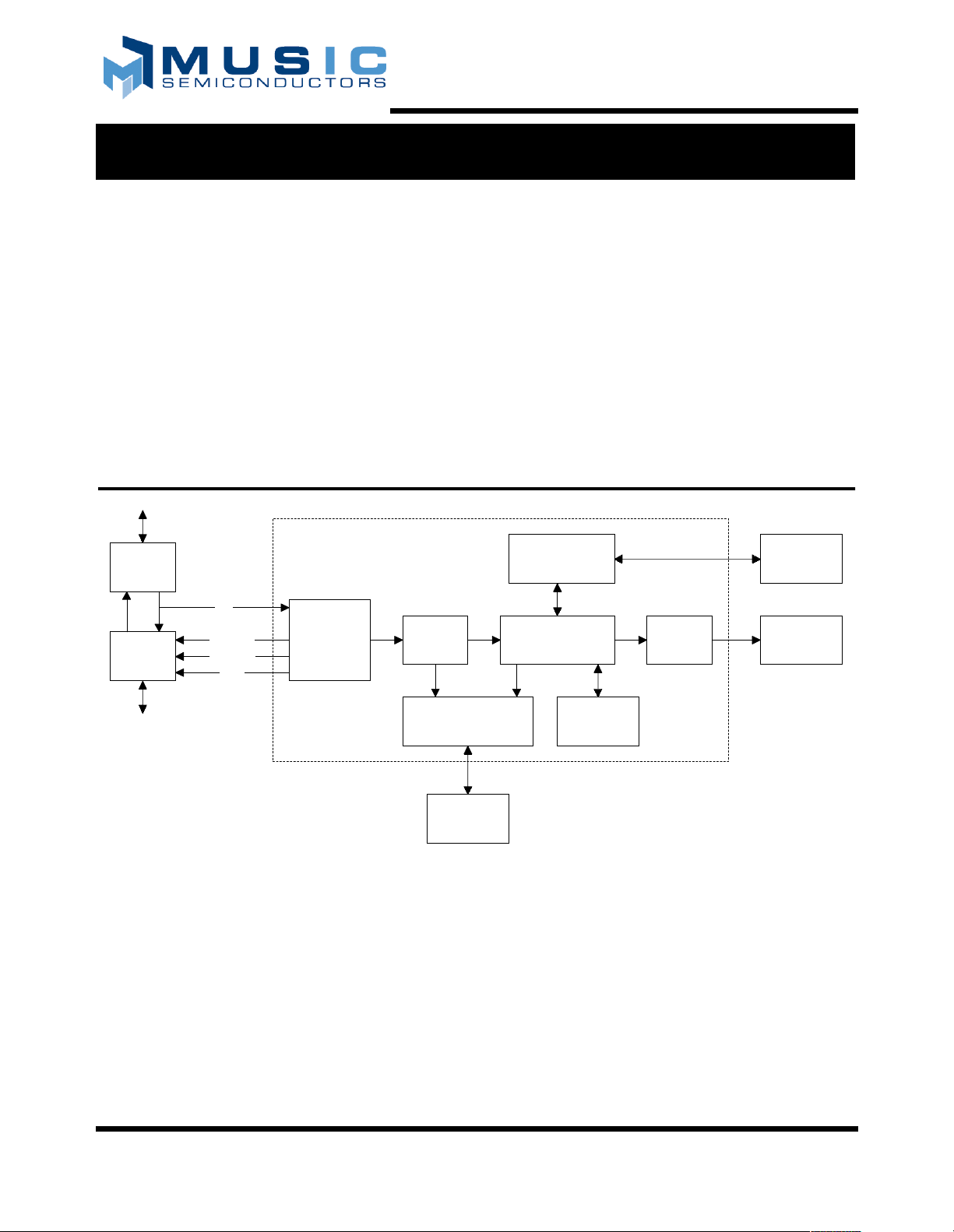
MUSIC
10/100
PHY
10/100
MAC
MII
REJECT
FR_ERR
TAG
MU9C8338
MII and
TAG Port
Packet
Parser
DISTINCTIVE CHARACTERISTICS
• Industry-standard 10/100Mb MII port
• Supports station list up to 32K addresses
• Port ID and MAC Frame Reject signal based on DA
search results
• Read search results from the Result port or CPU port
• Hardware support for Tag switching
• Optional automatic learning of new SAs
• Optional automatic Aging and Purging
• 144–pin LQFP packages
• 3.3 Volt operation with 5 Volt tolerant I/O
Processor
Interface
Controller
Result
Port
Processor
ASIC
LANCAM
Interface
MUSIC
LANCAM
Figure 1: System Application Diagram
MUSIC Semiconductors, th e MUSIC logo, and the phrase "MUSIC Semiconductors" are March 27, 2001 Rev. 1a
Registered trademarks of MUSIC Semiconductors. MUSIC and Epoch are a trademarks of
MUSIC Semiconductors.
Registers
Page 2

MU9C8338 10/100Mb Ethernet Filter Interface General Description
GENERAL DESCRIPTION
The MU9C8338, when configured with the MUSIC
Semiconductors MU9Cx480B family of LANCAMs
provides a high performance, large capacity Ethernet
address processing subsystem for use in Ethernet bridge,
OPERATIONAL OVERVIEW
Because of the flexibility of the MU9C8338, the best way
to approach the feature set of the device is to first look at a
typical 10/100Mb Ethernet application. The MU9C8338
captures the Destination address (DA) and the Source
address (SA) of an incoming Ethernet frame on the MII
port. After checking for a frame error or collision, the DA
is processed and the result (associated data, usually a port
ID) is made available. The SA then is checked, and either
learned if new, or aged if already in the list.
Typ ical MU9C8338 Application
The MU9C8338 plays an integral role in the example of
an Ethernet bridge system, shown in Figure 1.
This system can handle up to 32,768 addresses on a
bidirectional 100Mb Ethernet port by utilizing the
MU9C8338 device and four LANCAMs connected as
shown in Figure 1. The MII bus is "tapped" to collect
packet data as it passes from the Ethernet PHY to the
MAC. That data is processed automatically by the
MU9C8338/LANCAM combination. The MU9C8338
transfers the DA and SA to the CAMs for comparison. The
results of MU9C8338/LANCAM data processing are
available through the Result bus or through the Processor
bus. In addition to the Result bus, there is a serial Tag port
switch, or remote access products. The device is designed
to work in single-port system supporting a 100Mb/s
Ethernet port at wire speed.
for the MII port to relay the Tag ID to the system for
systems that support Tag switching.
When the DA is processed, the MU9C8338 first checks if
the frame is Unicast, Multicast, or Broadcast. Unicast
frames destined for the same collision domain (visible on
the same switch port as it came in on) are rejected. If the
DA is found in the CAM database, the port ID associated
with it is stored in the Result register. Multicast and
Broadcast frames are not processed by the system. Instead
they are identified and their classification is stored in the
Result register. Once processing completes, the Result
register is accessed through the Result port or Processor
port.
Provided the frame length is correct, and no errors are
detected, the SA is processed. If the SA exists in the CAM
database, the time stamp and Port ID are updated. If the
SA is not found in the CAM database, the address is
learned automatically, along with its Port ID and the
current time stamp information.
Address processing always has priority over management
routines, such as purging aged entries, inserting permanent
entries, deleting entries, or reading from the CAM
database.
2Rev. 1a
Page 3

Pin Descriptions MU9C8338 10/100Mb Ethernet Filter Interface
PIN DESCRIPTIONS
Note: All signals are implemented in CMOS technology with TTL levels. Signal names that start with a slash (“/”) are active LOW.
Inputs should never be left floating. Refer to the Electrical Characteristics section for more information.
/WRITE
/PCSS
PROC_RDY
/ INTR
GND
/RESET
INCR
VDD
/PCS
VDD
D1
D0
GND
A7
A6
A5
A4
A3
A2A1A0
VDD
D6
D4
D5
D3
D2
D7
D12
D13
D11
D10
D9
D8
D14
GND
VDD
RP0
RP1
RP2
RP3
GND
RP4
RP5
RP6
VDD
RP7
RP8
RP9
RP10
RP11
RP12
GND
RP13
RP14
RP15
RP_DV
VDD
SC_ENB
TST_HLD
GND
TST_HLD2
VDD
RP_NXT
RP_SEL
GND
GND
1
144
6
12
18
NC
NC
NC
NC
NC
24
30
36
138
42
132
48
126
54
120
60
114
66
108
102
VDD
D15
NC
/RESET_LC
/W
/E
/CM
/EC
GND
/MI
/FI
96
90
84
78
72
VDD
DQ0
DQ1
GND
DQ2
DQ3
DQ4
DQ5
VDD
DQ6
NC
DQ7
DQ8
DQ9
DQ10
GND
DQ11
DQ12
DQ13
NC
DQ14
DQ15
GND
SYSCLK
NC
NCNCNCNCNCNCNCNCNC
TP_SD
FRX_ER
GND
TP_DV
NC
VDD
REJ
Figure 2: Pinout
MII Interface
RXD[3:0] (Receive Data, Input, TTL)
RXD[3:0] is the 4-bit MII Receive Data nibble (see
Timing Diagrams: Timing Data for RXD, RX_DV, and
RX_ER).
RX_DV (Receive Data Valid, Input, TTL)
Data Valid is on RX_DV; RX_DV is asserted by the PHY
at the beginning of the first nibble of the data frame and
deasserted at the end of the last nibble of the frame. It
indicates that the data is synchronous to RX_CLK and is
itself synchronous to the clock (see Timing Diagrams:
Timing Data for RXD, RX_DV, and RX_ER).
RX_ER (Receive Error, Input, TTL)
RX_ER indicates a data symbol error in 100Mb/s mode or
Rev. 1a
3
NC
GND
RXD3
RXD0
RXD1
RXD2
VDD
RX_DV
RX_CLK
COL
RX_ER
CRS
GND
TDO
GND
TDI
TCK
VDD
TMS
/TRST
any other error that the PHY can detect, even if the MAC
is not capable of detecting that error (see Timing
Diagrams: Timing Data for RXD, RX_DV, and RX_ER).
RX_CLK (Receive Clock, Input, TTL)
RX_CLK is the receive clock recovered from the data by
the PHY. It is equal to 25MHz in 100Base-X mode or
2.5MHz in 10Base-X mode.
CRS (Carrier Sense, Input, TTL)
Carrier sense CRS indicates that the medium is active
(non-idle) and remains asserted during a collision. For Rx
or Tx: CRS is HIGH in 10/100Base-X half-duplex mode;
for Rx it is HIGH in repeater, full-duplex, and loopback
modes. CRS is not synchronized to RX_CLK.
Page 4

MU9C8338 10/100Mb Ethernet Filter Interface Pin Descriptions
COL (Collision, Input, TTL)
Collision detect COL is asserted by the PHY upon
detection of a collision on the medium and remains
asserted as long as the collision persists. It is HIGH in
half-duplex modes and remains HIGH for 1 microsecond
following the end of transmission; it is LOW in
full-duplex mode. It is asserted in response to
signal_quality_error message from the PMA in 10Base-X
Heartbeat mode.
Tag Port Interface
REJ (Reject, Output, TTL)
REJ is the reject packet command issued by the
MU9C8338. REJ is driven HIGH to reject a data frame,
and can be detected by and responded to by the MAC
device from 2 bit times after SFD to 512 bit times (64 byte
times) after SFD. The REJ signal can be made active
LOW by setting Bit 0 in the SSCFG register. (See Timing
Diagrams: REJ Timing Data.
FRX_ER (Frame Error, Output, TTL)
The Forced Receive Error pins provide the logical OR of
the RX_ER and REJ lines for the MII port (see Timing
Diagrams: Timing Data for FRX_ER in Relation to REJ
and RX_ER).
TP_SD (Ta g Port Data, Output, TTL)
The Tag Port Serial Data pin carries the destination Port
ID to external circuitry as soon as it is collected from the
CAM (see Timing Diagrams: Timing Data for Tag Ports
TP_DV and TP_SD).
TP_DV (Tag Port Data Valid, Output, TTL)
The Tag Port Data Valid pin is driven HIGH for as long as
unread data exists for the Destination Port ID. Pin TP_SD
carries the Destination Port ID (6 bits) to external circuitry
as soon as it is collected from the CAM (see Timing
Diagrams: Timing Data for Tag Ports TP_DV and
TP_SD).
Result Port Interface
See Timing Diagrams: Timing Data for Result Port
Interface. Table 1 shows the Result Port bit descriptions.
Note: Although the result data register can also be read through
the processor port, it is important to note that the means of
retrieving the data must be unique. Therefore, if the user is not
using the Result Port Interface, but is reading result data through
the processor port, RP_NXT and RP_SEL should be pulled low.
This ensures that all result data remains in the Result Data
register until read through the processor port. RP_NXT and
RP_SEL should be pulled low to 0 volts through a pull-down
resistor (typically 10k ohms).
RP[15:0] (Result Port Data, Output, Tri-state, TTL)
The Result Port Data carries the results of recently
processed packets detected on the MII port. See Table 1
for details of the Result Port Data bit descriptions. These
are identical to the Result Data register bits.
RP_DV (Result Port Data Valid, Output TTL)
The Result Port Data Valid indicates that the RP port
carries valid packet data. As long as there is valid packet
data, RP_DV will stay HIGH.
RP_NXT (Result Port Next Data, Input, TTL)
The Result Port Next pin brings the next result to the RP
bus if RP_SEL is asserted. If there are no additional results
available, the RP_DV will drop LOW after the time
interval specified in the Result Port Timing specification.
RP_SEL (Result Port Select, Input, TTL)
The Result Port Select pin controls RP[15:0] and
RP_NXT. RP_NXT and RP_SEL are connected by a
logical AND. Therefore, RP_SEL must be HIGH in order
for RP_NXT to bring the next result to the RP bus.
RP_SEL can stay continuously HIGH as long as there is
valid packet data, RP_DV will stay HIGH.
Table 1: Result Port Bit Descriptions
Bit(s) Description
15:10 6-Bit Source Port ID
9:8 Packet Type: Broadcast = 00, Multicast = 01,
Unicast = 10
7 (if Unicast) Match Found
6:1 6-Bit (if CAM Match Found) Destination Port ID
0 (If Match Found) Destination Port = Source Port
Control Interfaces
See Timing Diagrams: Timing Data for Control Interfaces.
SYSCLK (System Clock, Input, TTL)
CLK is the user-supplied system clock for synchronous
chip operation; its frequency must be 25-50 MHz with
duty cycle between 45 to 55 percent.
/RESET (Reset, Input, TTL)
When system Reset is taken LOW, all internal
state-machines are reset to their initial state and any data is
cleared. All registers are returned to default values.
/RESET is synchronous and should be held LOW for a
minimum of two SYSCLK cycles. The user must set the
LANCAM Segment Control register after asserting
/RESET.
4Rev. 1a
Page 5

Pin Descriptions MU9C8338 10/100Mb Ethernet Filter Interface
INCR (Increment Time Stamp Counters, Input, TTL)
INCR is a user command to invoke the built-in purge
routine. Both STCURR and STPURG 8-bit counters are
advanced one count on the rising edge of INCR, and the
time stamp stored with each LANCAM entry is compared
with STPURG. Matching entries subsequently are purged
or deleted. This pin must be configured, if it is required, by
setting bit 2 and bit 3 in the System Target (STARG)
register. Each counter can be incremented individually
through the Processor Port. (see Operational
Characteristics: STARG System Target Register
Mapping).
Host Processor Interface
The Host Processor interface is asynchronous to the
System Clock. This interface is controlled by the /PCS or
/PCSS (whichever is appropriate) and PROC_RDY
signals, which form the handshaking between the
processor and the MU9C8338. This allows the end system
to use a processor that runs at a different clock speed than
the clock required by the MU9C8338. (see Timing
Diagrams: Timing Data for Host Processor Interface).
/PCS (Processor Port Chip Select, Input, TTL)
Processor Chip Select is taken LOW by the host processor
to gain access to the MU9C8338 Port or Chip registers.
/PCSS (Processor Port Chip Select System, Input, TTL)
Processor Chip Select System is taken LOW by the host
processor to gain access to the MU9C8338 System
registers or to access the LANCAM.
/WRITE (Processor Port Read/Write, Input, TTL)
Read/Write determines the direction of data flow into or
out of the MU9C8338 host processor interface. If /WRITE
is LOW, the data is written into the register selected by
A[7:0] and /PCS or /PCSS; if HIGH, the data is read from
the register selected by A[7:0] and /PCS or /PCSS.
A[7:0] (Processor Port Address, Input, TTL)
Processor Address bus A[7:0] selects the MU9C8338
register accessed by the host processor.
D[15:0] (Processor Port Data, Input/Output, Tri-state, TTL)
Processor Data bus D[15:0] is the tri-state processor data
bus for the MU9C8338.
PROC_RDY (Processor Port Ready, Output, Tri-state, TTL)
When reading from or writing to any MU9C8338 internal
register, the PROC_RDY tri-state output goes LOW on the
falling edge of /PCS or /PCSS. If it is a read cycle,
PROC_RDY goes HIGH on the rising edge of SYSCLK
once data is available. If it is a write cycle, PROC_RDY
goes HIGH on the rising edge of SYSCLK when the
internal register is ready to accept data.
/INTR (Processor Interrupt, Output, TTL)
/INTR goes LOW to signal that one of the four
configurable interrupt conditions have been satisfied. The
four separate conditions are configured by setting bits in
the appropriate register. /INTR returns HIGH when the
appropriate register is read. See Table 2 for details of
which interrupt conditions are possible and which register
must be read to reset the /INTR pin to HIGH.
Table 2: /INTR Settings
Register R equired to
Select Interrupt
Condition
PTARG RSTAT. Please note that /INTR will only return
STARG SSTAT. Please note that /INTR will only return
Rev. 1a
5
To clear /INTR, Read Interrupt Condition
HIGH when all possible result data has been read.
HIGH when the LANCAM has become not full.
Therefore, after the SSTA T register read has
confirm e d th e status of the in te r r u pt c on d ition, an
entry should be removed from the LANCAM by
using the PURGE sequence.
The MII port ha s parsed an incoming packet. The DA lookup
has been performed and the result data is available to be
read from RDAT register.
The /FF output from the LANCAM (s) has indicated that the
LANCAM is full. When reading the SSTAT register, a full
condition is indicated by bit 0 = 0.
Page 6

MU9C8338 10/100Mb Ethernet Filter Interface Pin Descriptions
LANCAM Interface
See Timing Diagrams: Timing Data for LANCAM
Interface.
DQ[15:0] (LANCAM Bus, Input/Output, Tri-state, TTL)
DQ[15: 0] tri-state 16- bit bus transfers data or instructions
between the MU9C8338 and the LANCAM. When no
data or instructions are present on the bus, the bus goes
HIGH-Z.
/E (LANCAM Bus Enable, Output, Tri-state, TTL)
The /E chip enable is taken LOW to initiate LANCAM
activity. On LANCAM read cycles, /E is taken HIGH after
the MU9C8338 registers the data.
/W (LANCAM Bus Write, Output, Tri-state, TTL)
The MU9C8338 outputs /W (read/write select) to control
the direction of data flow between the MU9C8338 and the
LANCAM. If /W is LOW at the falling edge of /E, the
MU9C8338 outputs data on the DQ[15:0] bus for the
LANCAM as input. When /W is HIGH at the falling edge
of /E, the LANCAM outputs data on the DQ[15:0] bus to
the MU9C8338 as input.
/CM (LANCAM Bus Command Mode, Output, Tri-state, TTL)
The MU9C8338 outputs /CM Data/Command Select to
control whether the LANCAM interprets the DQ[15:0]
bus contents as command information or data. If both /CM
and /W are LOW at the falling edge of /E, the MU9C8338
outputs an instruction for the LANCAM to execute or a
value for one of the LANCAM configuration registers. If
/CM is LOW while /W is HIGH, then the LANCAM will
output data from one of its configuration registers to the
MU9C8338. If /CM is HIGH while /W is LOW, the
MU9C8338 will output data for the LANCAM to place in
one of its data registers or memory. If /CM is HIGH while
/W is HIGH, the LANCAM outputs data from one of its
data registers or memory to the MU9C8338.
/EC (LANCAM Bus Enable Chain, Output, Tri-state, TTL)
The Daisy Chain Enable signal performs two functions.
The /EC signal enables the LANCAMs /MF output to
show the results of a comparison. If /EC is LOW at the
falling edge of /E in a cycle, the /MF flag output is
enabled; otherwise, /MF is held HIGH. The /EC signal
also enables the /MF-/MI daisy chain that serves to select
the device with the highest-priority match in a string of
LANCAMs.
/MI (LANCAM Bus Match Flag, Input, TTL)
The /MI LANCAM Match flag input is used to indicate to
the MU9C8338 the conditions of the LANCAM Match
flag. The /MF output from the LANCAM should be
connected to this pin. If more than one LANCAM is used,
/MI should be connected to the /MF pin of the last
LANCAM in the daisy chain.
/FI (LANCAM Bus Full Flag, Input, TTL)
The /FI LANCAM Full flag input is used to indicate to the
MU9C8338 the condition of the LANCAM Full flag. The
/FF output from the LANCAM should be connected to this
pin. If more than one LANCAM is used, /FI should be
connected to the /FF of the last device in the daisy chain.
/RESET_LC (Reset LANCAM, Output, TTL)
/RESET_LC is LOW whenever /RESET is LOW. It is
taken HIGH only by writing to bit 0 in the System
Dynamic Configuration (SDCFG) register. See SDCFG
register information.
Test
SC_ENB (Scan Enable)
Enables scan chain for testing. Pin may be left
unconnected or tied to GND for normal operation
TST_HLD, TST_HLD2 (Test Hold)
Enables test mechanism. Pins may be left unconnected or
tied to GND for normal operation.
JTAG
Note: Please refer to IEEE Standard 1149.1 for information on
using the mandatory JTAG functions. The optional HIGH-Z
function is implemented and may be activated by writing 0011 to
the JTAG Instruction register.
/TRST (JTAG Reset, Input)
The /TRST is the Test Reset pin. It is internally pulled up
with a 3k minimum resistor. It must be tied to /RESET or
tied LOW when the JTAG port is not used.
TMS (JTAG Test Mode Select, Input)
The TMS input is the Test Mode Select input. This pin is
internally pulled up with a 3k minimum resistor.
TCK (JTAG Test Clock, Input)
The TCK input is the Test Clock input. It can be tied at a
valid logic level 1 when not in use. This pin is internally
pulled up with a 3k minimum resistor.
TDI (JTAG Test Data Input, Input)
The TDI input is the Test Data input. This pin is internally
pulled up with a 3k minimum resistor.
TDO (JTAG Test Data Output, Output)
The TDO output is the Test Data output.
Po wer and Ground
VDD, GND (Positive Power Supply, Ground)
These pins are the power supply connections to the
MU9C8338. VDD must meet the voltage supply
requirements in the Operating Conditions section relative
to the GND pins, which are at 0 Volts (system reference
potential), for correct operation of the device.
6Rev. 1a
Page 7
Functional Description MU9C8338 10/100Mb Ethernet Filter Interface
FUNCTIONAL DESCRIPTION
Internal Functions
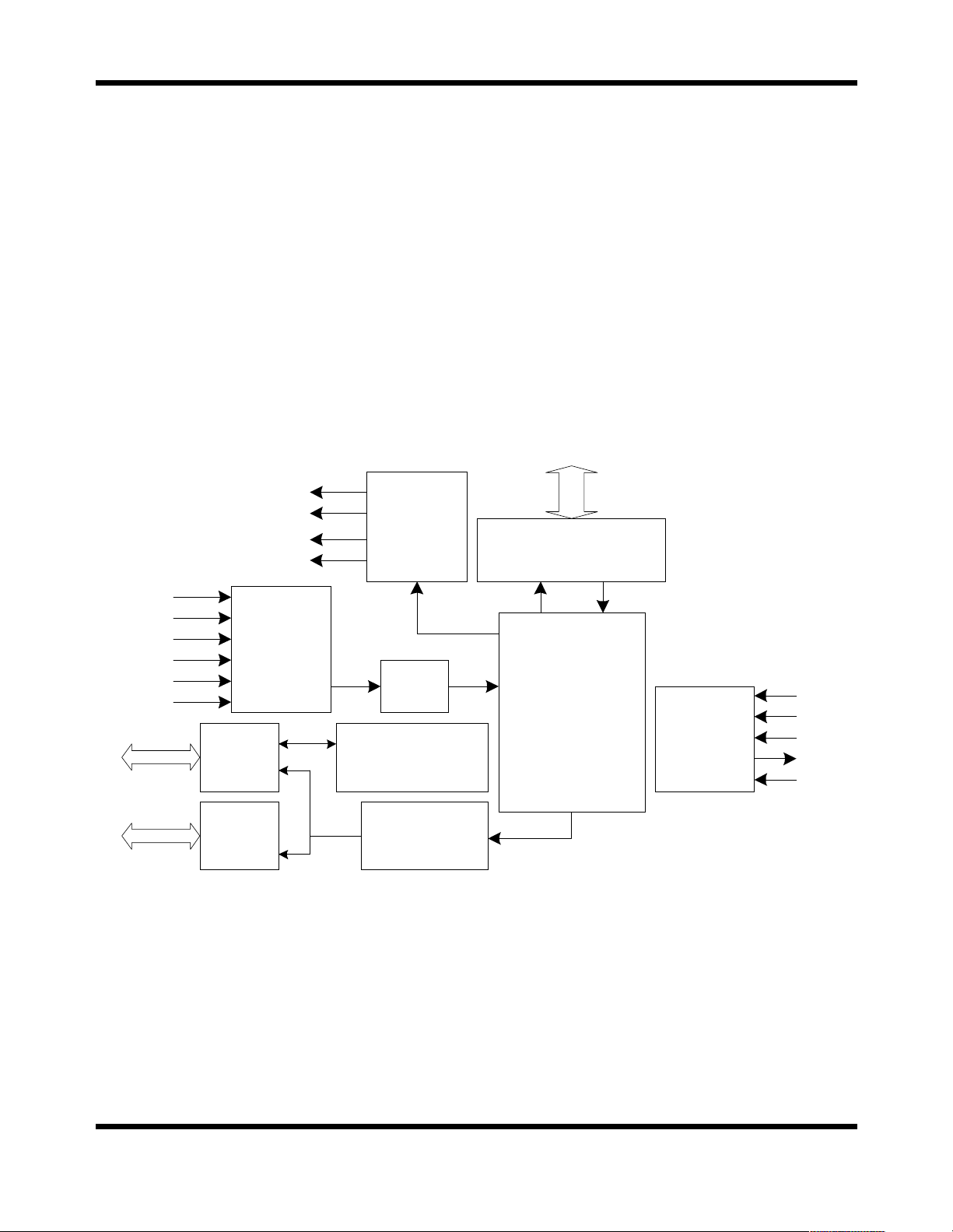
MU9C8338 internal functions are shown in Figure 3.
Before discussing the individual blocks, the underlying
principles are presented. The network interface is
monitored for network and data symbol errors. Receive
data [RXD] is clocked into a register using the 25MHz
recovered clock for 100Base-X or 2.5MHz clock for
10Base-X. The Preamble and Start Frame delimiter (SFD)
are scanned to locate the Destination address (DA) and the
Source address (SA).
The LANCTL block generates the command cycles and
operational codes to complete CPU-requested actions and
network-generated requests. The CPU must initialize the
CAM, write the permanent station list, and initiate other
housekeeping functions. Network traffic initiates DA
filtering, SA learning, and time stamp updates. All
state-machines required for real-time operations are
implemented in the ASIC hardware; the host CPU runs the
non-time-critical initialization routine.
The MU9C8338 schedules communication with the host
processor and the CAM through an arbitration process.
Once the system is initialized and configured,
highest-priority is given to network traffic.
FRX_ER
RX_DV
RX_ER
RXD[3:0]
RX_CLK
CRS
COL
CPU Bus
REJ
TP_SD
TP_DV
MII
Interface
Host CPU
Interface
Tag Port
Interface
MAC
Receiver
Configuration,
Control and Status
Registers
Information on the LANCAM operation and instruction
set can be found in the appropriate LANCAM data sheet
for each device.
LANCAM Bus
LANCAM
Interface
TCK
LANCTL
JTAG
Controller
TMS
TDI
TDO
/TRST
Result Bus
Rev. 1a
Result Bus
Interface
FIFO
Figure 3: Functional Block Diagram
7
Page 8

MU9C8338 10/100Mb Ethernet Filter Interface Functional Description
Destination Address Processing
Once configured, the MU9C8338 will extract the DA from
the frames that are received through the MII port. An
automatic address processing function is subsequently
triggered. Once the DA processing function is triggered,
the frame is monitored to detect whether it is a broadcast,
multicast, or unicast frame and the appropriate actions are
taken. DA processing consists of the following actions:
• Packets are characterized as Broadcast, Multicast, or
Unicast types.
• Unicast packets initiate a search of the CAM for
existing entries.
• If a DA match is found, the Port ID read from the
CAM is compared to the Source Port ID. If the Source
Port ID and Destination Port ID match, the frame is
rejected. If the Port IDs are different, the Tag
information is made available for MACs that support
Tag switching, through the Tag port.
• If the MU9C8338 rejects the frame, it asserts the
Reject output pin (REJ) and forces the MII RX_ER
output (FRX_ER) HIGH for the MII Port. This causes
the MAC to discard the frame.
• Once the DA processing function is complete, the
MU9C8338 stores the result. This result indicates the
characterization of the processed frame. (Broadcast,
Multicast, or Unicast) and the Source Port ID.
Additionally, if a unicast frame was processed, the
result of the search and the port ID of the DA is also
stored. Finally, the detail of whether the Destination
port and the Source port are identical is also stored.
• The result of DA processing may be read in two ways.
1. An interrupt may be sent to the host processor
indicating that there is a result available. The host
processor would read the result from an internal
Result Data register.
2. External circuitry can monitor the status of the
Result Port Data valid (RP_DV) output pin. This
output indicates that there is a result available in the
internal register which can be read through the Result
port. The external circuitry can read the data by
asserting the Result Port Select (RP_SEL) pin.
Assertion of Result Port Next (RP_NXT) clears the
value and advances the next entry if there is one
available.
Source Address Processing
Once configured, the MU9C8338 also will perform SA
processing functions after the address information has
been extracted from a received frame. The SA of each
arriving frame is stored by the MU9C8338 for further
processing, along with the port ID and the current time
stamp. Note that at start-up, permanent addresses and their
Port ID are loaded into the LANCAM through the CPU
port; as message traffic proceeds, new addresses are
learned and added to the LANCAM database, and aged
addresses are purged. SA processing consists of the
following actions:
• The SA field is collected and temporarily stored. Note
the SA cannot be a Broadcast or Multicast address by
definition.
• When the complete packet has arrived, the CRC field
is checked and the length of the packet is checked.
Any errors result in no further SA processing.
• If the packet did not contain any errors, (or the CRC
check facility is disabled), the SA field is compared
with the address fields that are stored in the
LANCAM.
• If a match is found, the Port ID and time stamp for
that entry are updated. If no match is found, the SA is
added to the CAM, along with the current time stamp
and the Port ID assigned to that particular Source port.
Functional Blocks
The building blocks that make up the MU9C8338 are
shown in Figure 3, and their functions are described by the
following.
MII Interface (MII Port)
The incoming asynchronous receive data is registered for
subsequent processing. MU9C8338 internal processing is
synchronous with the system clock.
Tag Port Interface (Tag P ort)
Rejection of a packet is indicated by the assertion of REJ.
The FRX_ER line, which otherwise reflects the state of
the RX_ER pin, is forced to HIGH at the same time. If the
DA is matched in the LANCAM, the TP_DV pin is
asserted and the destination port ID, high-order bit first, is
clocked out through the TP_SD pin transitioning after the
RX_CLK rising edge.
MAC Receiver
This block performs tasks that are a subset of the Ethernet
MAC. It detects errors, (CRS, COL, RX_ER, and Runt
Frame), determines the start of frame, parses addresses,
computes the CRC for 10Base-X packets, and formats the
4-bit nibbles into 48-bit SA and DA registers.
8Rev. 1a
Page 9
Functional Description MU9C8338 10/100Mb Ethernet Filter Interface
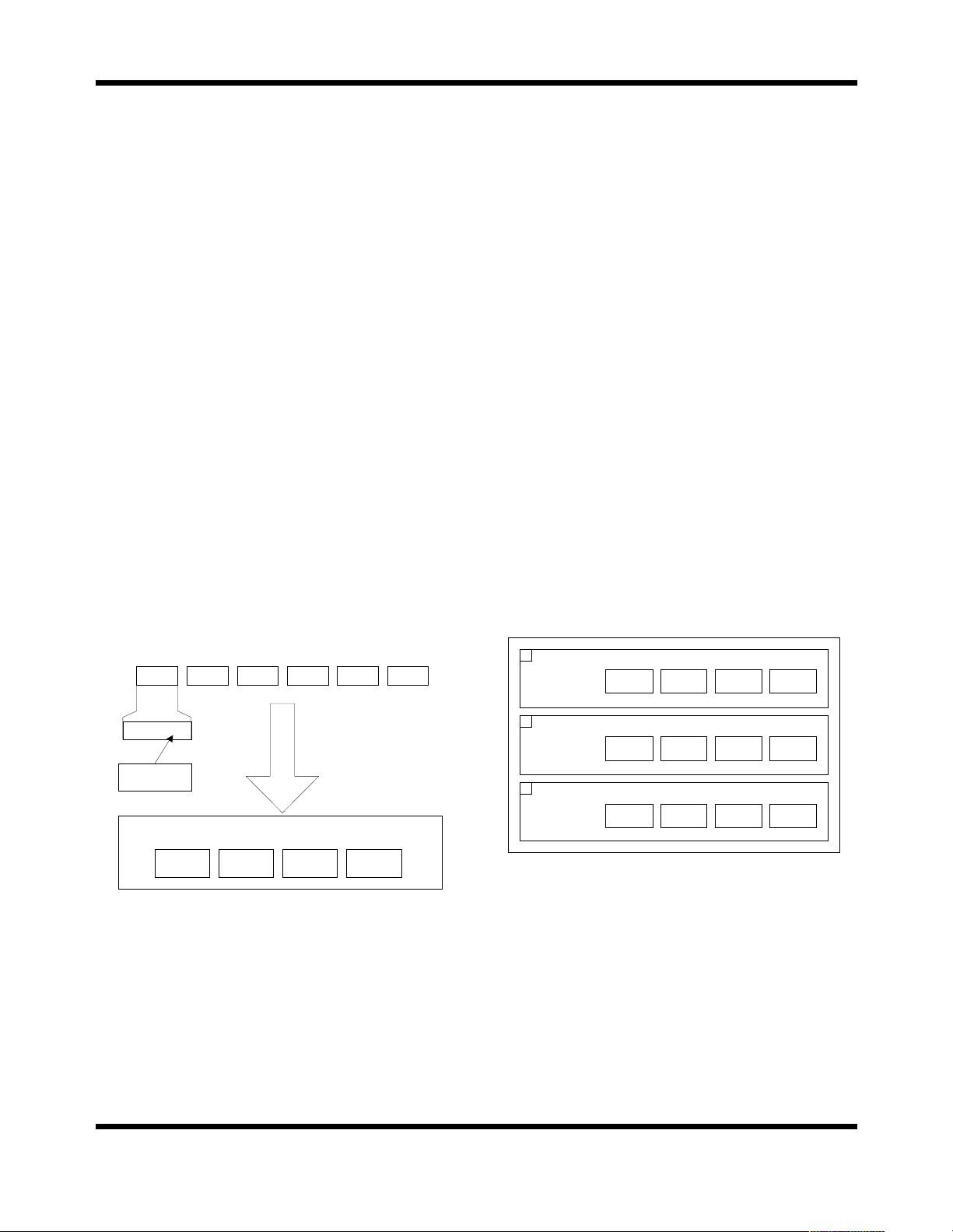
MAC Address Storage
When the MU9C8338 performs an SA processing
function, it automatically extracts the MAC address from
the packet. The database is searched and the MAC address
is added to the LANCAM database if necessary. Similarly,
when a DA processing function is performed, the
MU9C8338 automatically searches the database for the
extracted DA MAC address.
It is important that the user is aware of the byte ordering of
the 48-bit MAC address when it is stored in the LANCAM
database. This is because the user must byte-order MAC
addresses identically when a database entry is to be
manually added or deleted. Similarly, if the user wishes to
read out a MAC address, they should also be aware of the
byte ordering when the relevant data registers are read.
Throughout this data sheet MAC addresses are shown as
bit 47 being the most significant bit, which is placed on the
left. Similarly, bit 0 is shown as the least significant bit and
placed on the right. Using this notation, the
Individual/Group (I/G) bit subfield would be shown as bit
40. This bit would be the first bit of an address transmitted
If the MAC address shown in Figure 4 is added to the
database by the MU9C8338, it is stored as follows:
• Segment 3 = 6002h
• Segment 2 = 128Ch
• Segment 1 = 5634h
• Segment 0 = Associated data (permanent bit, time
stamp and port ID)
If the user wishes to use the built-in routines to manually
add, delete, or read MAC addresses from the database, the
System CAM Word registers (SCDW) are used as shown
in Figure 5. It shows how the MAC address, used as an
example in Figure 4, would be transferred using the
SCDW registers.
If the user intended to delete the MAC address, the SCDW
registers would be written as shown in item 1 and the
SDO_DELETE routine would be invoked.
If the user intended to add the address manually, the
SCDW registers would be written as shown in item 2 and
the SDO_ADD routine would be invoked.
onto the serial network and also the first bit received. The
IEEE 802.3 refers to the I/G bit subfield as bit 0. If the bit
is set to 1, it indicates that the address is a group address.
Conversely, if the bit is set to 0, it indicates it is an
individual address. Figure 4 shows a typical 48-bit MAC
address used in Ethernet or IEEE 802.3 networks.
47 40 162324313239 070815 00
:::::
02 5634128C60
MAC Address
Finally, if the user intended to read an entry, the
SDO_READ routine would be invoked and the address
would be read from the SCDW registers as shown in item
3. The built-in routines are explained more fully later in
this document.
1
SDO_DELETE
SCDW3 SCDW2 SCDW1 SCDW0
6002not used 5634128C
IEEE bit 0
Rev. 1a
0000 0010
I/G bit
LANCAM Database Entry
seg 3 seg 2 seg 1 seg 0
6002 assoc. data5634128C
Figure 4: MAC Address Byte Order
9
2
SDO_ADD
3
SDO_READ
SCDW3 SCDW2 SCDW1 SCDW0
6002 assoc. data5634128C
SCDW3 SCDW2 SCDW1 SCDW0
6002 assoc. data5634128C
Figure 5: SCDW Register Order
Page 10

MU9C8338 10/100Mb Ethernet Filter Interface Functional Description
LANCAM Sequencer
The sequencer is a state machine that generates the control
signals required for CAM read and write cycles, and
multiplexes appropriate data and operational codes to
LANCAM data lines. The sequencer operations are:
• Execute LANCAM cycles for CPU port
• DA processing
• SA processing
• Purging of aged entries
• Add Permanent Entries to LANCAM database
• Delete Entries from LANCAM database
• Read Entries from the LANCAM database.
FIFO and Result Port
When the DA sequence is executed, the result is stored in
a FIFO for later collection by either the CPU over the
Processor Bus from the Result register, or by external
hardware attached to the Result port.
Initialization
At power-up or after a hardware reset, the host processor
should download the LANCAM configuration and register
contents to enable the LANCAM to operate as required.
The LANCAM initialization and configuration that is
downloaded by the CPU should do the following: The
individual Page Address registers of each LANCAM in
the LANCAM chain should be set with appropriate values.
The Foreground Register set should be set to allow normal
DA and SA filtering. This involves setting the Control,
Segment Control, and Mask registers to suit. The
Background Register set should be set to allow the
background management tasks to be preformed. This
involves setting the Control, Segment Control, and Mask
registers to suit. The LANCAM should be configured to
store 48-bit MAC addresses in segments 3–1 and the
associated data in segment 0. The allocation of bits in the
16-bit associated data segment is specified in the
description of the SCDW0 Association Data register.
Permanent Station Addresses
Using the Add Entry routine, the nonvolatile station list
can be added to the LANCAM by the host processor. The
Associated Data bit 15 is set to 1, to indicate a permanent
entry. Permanent entries are removed only with the Delete
Entry routine.
Management
The Delete Entry and Read Entry routines are available for
database maintenance and housekeeping. Although
permanent addresses cannot be purged, they can be deleted
using the management Delete Entry routine.
Aging and Purging
Time stamps are added automatically to the LANCAM
entries by the MU9C8338. Two counters are provided to
store the current and purge time stamps. The Current Time
Stamp is the 8-bit value that automatically is added or
updated when a SA processing function is completed. The
Purge Time stamp is the 8-bit value that is compared with
the 8-bit time stamps stored with the LANCAM entries
during purges. The initial value of the counters are
STPURG = 01H and STCURR = 00H. The counters may
be incremented individually through the CPU commands.
Either the CPU or the external INCR pin can increment
both counters simultaneously. Whenever STPURG is
incremented, a purge operation is initiated. The counters
roll-over so the times should be thought of as slots to be
used and reused in a round-robin fashion.
The existence of two counters (time stamps) allows the
data-aging rate to be varied according to network traffic
density. When the difference between the counters is large
(default), the address data is purged less frequently;
shrinking the counter difference causes the data to age
sooner. Incoming SAs are time stamped or updated with
the current value of STCURR. Older entries time stamped
with the same value as STPURG are purged upon the
increment of STPURG. The permanent address database
built using the Add routine is not affected by time stamps.
The data age gap is effectively the length of time an entry
will exist in the LANCAM database if it is not updated.
This gap is the difference between the STCURR and
STPURG counter. When network traffic is low, STCURR
may be increased in order to increase the length of time an
entry will exist. When network traffic is high, STPURG
may be increased in order to decrease the length of time an
entry will exist. When STPURG is incremented older
entries are also purged from the database if their time
stamp matches STPURG.
STCURR and STPURG may be incremented
simultaneously to keep the data age gap constant and to
purge the older entries from the database.
To maintain "current" time, STCURR is advanced in any
one of the three ways:
1. The CPU issues an increment STCURR command.
Only the STCURR counter is increased.
2. The CPU issues an increment STCURR and STPURG
command. Both counters are increased simultaneously.
3. The INCR pin is asserted. Both counters are increased
simultaneously.
To maintain "purge" time and to purge aged CAM entries,
STPURG is advanced in any one of the following three
ways:
10 Rev. 1a
Page 11

Functional Description MU9C8338 10/100Mb Ethernet Filter Interface
1. The CPU issues an increment STPURG command.
Only the STPURG counter is increased.
2. The CPU issues an increment STCURR and STPURG
command. Both counters are increased simultaneously.
3. The INCR pin is asserted. Both counters are increased
simultaneously.
If the STPURG value was incremented, the MU9C8338
initiates a purge operation using the new STPURG value.
STPURG should never be incremented to equal STCURR.
The time stamping of LANCAM entries and the procedure
required to initiate a purge is explained as follows:
1. Incoming SAs to be learned are associated with the
most recent STCURR value. The time stamps of each
SA already in the CAM database is updated to
STCURR, each time a packet with that SA is processed.
2. STPURG and STCURR are advanced as described
earlier to purge entries that have the same time stamp
value as STCURR.
Following is an example, beginning with the defaults,
initially, STCURR = 00H and STPURG = 01H. As
packets arrive, learned or refreshed, SAs are labeled with
STCURR = 00H. (At that moment STPURG = 01H).
Increment, either hardware or software initiated, results in
STCURR = 01H and STPURG=02H.
A purge operation is initiated that will eliminate all CAM
entries with time stamp = 02H. The oldest entries (SAs)
that have not been updated in 255 increment times are
purged automatically without further involvement.
If the CAM Full flag is asserted, an interrupt (if
configured) to the CPU is generated. Assume that
STCURR = F0H, and STPURG = F1H. The CPU may
initiate an increment STPURG operation so that older
entries may be purged. This increases the value of
STPURG to F2H. A purge operation is initiated that will
eliminate all CAM entries with time stamp = F2H.
The CPU should monitor the System Status register, and if
the CAM is still full, the operation can be repeated until
entries are purged and the CAM Full flag is de-asserted.
Assume that STPURG was incremented 128 times. This
would purge the oldest half of the time stamp values and
thus, reduce the maximum age to half the previous 255.
This can be accomplished without disturbing ongoing
normal increment time stamp update operations.
CRC and Other Data Integrity Checks
For 10Base-X packets, a 32-bit cyclic redundancy check is
calculated from the data frame (exclusive of the preamble
and start frame delimiter) and compared to the frame
check sequence (FCS). This check is only performed if the
PCFG register is set accordingly to enable the facility.
Also, according to the MII interface specifications, the
RX_ER, CRS, and COL signals are monitored and error
conditions are recognized. If any error is identified, the
source address is not processed. This is intended to
maintain the integrity of the LANCAM database.
Rev. 1a
11
Page 12

MU9C8338 10/100Mb Ethernet Filter Interface Software Model
SOFTWARE MODEL
System Registers
One set of registers is available to address the MU9C8338
component and its attached LANCAMs as a single system.
The application decodes one range of addresses to produce
Table 3: System Registers
Name R/W Description Address Default Settings
SSTAT R System Status SYSTEM_BASE + 0H N/A
SSCFG W System Static Configuration SYSTEM_BASE + 1H 0000H
SDCFG W Syst em Dynamic Configuration SYSTEM_BASE + 2H 0H
STARG W System Targets SYSTEM_BASE + 3H 0H
SCDW0 R/W CAM Data Word 0 SYSTEM_BASE + 5H N/A
SCDW1 R/W CAM Data Word 1 SYSTEM_BASE + 6H N/A
SCDW2 R/W CAM Data Word 2 SYSTEM_BASE + 7H N/A
SCDW3 R/W CAM Data Word 3 SYSTEM_BASE + 8H N/A
STPURG R Time Stamp to Purge SYSTEM_BASE + 9H 01H
STCURR R Time Stamp Current SYSTEM_BASE + AH 00H
SMXSADACYC W Max SA/DA Cycle SYSTEM_BASE + CH 20H
SCSWB R CAM Status Word B SYSTEM_BASE + DH N/A
SCSWA R CAM Status Word A SYSTEM_BASE + EH N/A
SSAU W SA Update Op-Co de SYSTEM_BASE + 10 H 0368H
SSAL W SA Learn Op-Code SYSTEM_BASE + 11H 0334H
SLCCS W LANCAM Control Signals SYSTEM_BASE + 12H 0FH
SDO_DELETE W Perform Delete Sequence SYSTEM_BASE + 20H N/A
SDO_ADD W Perform Add Sequence SYSTEM_BASE + 21H N/A
SDO_READ W Perform Read Sequence SYSTEM_BASE + 24H N/A
SDO_INCTS W Perform Increment STCURR Sequence SYSTEM_BASE + 26H N/A
SDO_INCPR W Perform Increment STPURG Sequence SYSTEM_BASE + 27H N/A
SDO_INCTSPR W Perform Increment STCURR & STPURG Sequence SYSTEM_BASE + 28H N/A
SDO_SETADD W Perform SetAddr. Sequence SYSTEM_BASE + 29H N/A
a Processor Chip Select System signal (/PCSS). The
lowest address in this application-defined address range,
shown in Table 3, is referred to as SYSTEM_BASE.
System Status Register
The System Status register (SSTAT) provides a CPU
visibility into the state of the LANCAM array. The /FF bit
indicates the current state of the Full Flag output of the
LANCAM array. The /MF bit indicates the Match Flag
output of the LANCAM array.
Table 4: SSTAT: System Status Register Mapping
Name Bits Description
/FF 0 Full Flag from LANCAM array
/MF 1 Match Fl ag from LANCAM array
System Static Configuration Register
The System Static Configuration register (SSCFG) allows
the CPU to configure the LANCAM array. These are set
and forget values. The CAM_SPD sets the controller to
match the speed grade of the LANCAM components
attached. A 50MHz clock is assumed. The INV_REJ bit
configures the REJ port to be active LOW instead of active
HIGH.
Table 5 shows a CAM_SPD setting for a 120 ns speed
grade LANCAM component. 120 ns LANCAMs are no
longer available and it is recommended that when using a
90 ns LANCAM, set SSCFG[3:1] to 000. This setting
accommodates most applications and has the added
benefit of using the least amount of power.
Table 5: SSCFG: System Static Configuration
Register
Name Bits Description
CAM_SPD 3:1 000 = 120 ns (90 ns)
001 = 90 ns
010 = 70 ns
011 = RESERVED
100 = RESERVED
101 = RESERVED
110 = RESERVED
111 = RESERVED
INV_REJ 0 0 = Active HIGH
1 = Active LOW
12 Rev. 1a
Page 13

Software Model MU9C8338 10/100Mb Ethernet Filter Interface
The System Dynamic Configuration Register
The System Dynamic Configuration Register (SDCFG)
allows the CPU to control the MU9C8338 /RESET_LC
output pin. This pin normally would be connected to the
/RESET input of all the LANCAMs in a chain of
LANCAMs. When the RST_CAM bit is logic 0 the
/RESET_LC output is LOW and when the RST_CAM bit
is logic 1 the /RESET_LC output is HIGH. Note that if a
hardware reset is performed by taking the MU9C8338
/RESET input LOW, /RESET_LC is asserted LOW.
However once /RESET has been taken HIGH,
/RESET_LC remains LOW, holding the LANCAM(s) in
the reset condition. The RST_CAM bit must be set to 1 to
return /RESET_LC HIGH and hence allow the
LANCAMs to operate normally.
Table 6: SDCFG System Dynamic Configuration
Register
Name Bits Description
RST_CAM 0 0: Reset
1: Normal Operation
System Target Register
The System Target Register (STARG) allows the CPU to
determine how events are to be handled. The INCR_PIN
bits enable or disable to INCR hardware input. The
EN_FF_INT bits enable or disable whether the LANCAM
/FF output will produce an interrupt when the LANCAM
is full.
Table 7: STARG: System Target Register Mapping
Name Bits Description
INCR_PIN 3:2 00: Disable INCR pin
01: RESERVED
10: RESERVED
11: Enable INCR pin
EN_FF_I N T 1:0 00: Disable /FI int er r u p t
01: RESERVED
10: Enable /FI inte rr u pt
11: RESERVED
System CAM Word Registers
When using the series of built-in routines, the SCDW
registers are used to transfer data. The bit mapping is
different for each routine. Please refer to the appropriate
mapping for the relevant routine. Also refer to section
MAC Address Storage on page 9.
Table 8: SCDW: Data Mapping
Contents
Name SDO_DELETE
Sequence
SCDW0 [15:0] MAC_AD [15:0] Associated data
SCDW1 [15:0] MAC_AD [31:16] MAC_AD [1 5: 0]
SCDW2 [15:0] MAC_AD [47:32] MAC_AD [31:16]
SCDW3 [15:0] Not used MAC_AD [47:32]
Other Routines
During the LANCAM initialization and configuration
process, SCDW0 is used with SLCSS to configure the
LANCAMs. When SCDW0 is used to transfer associated
data, the bit mapping is as shown in Table 9.
SCDW0 has an additional purpose that allows the
associated data to be read after a DA processing function
has completed. After every DA is processed, the
associated data read from the LANCAM is placed in the
SCDW0 register, Therefore, if the system software reads
the SCDW0 register after a packet is processed, the Port
ID, Timestamp, and permanent bit information may be
found.
Table 9: SCDW0: Associated Data Register
Mapping
Name Bits
Time_Stamp 7:0
Port_ID 13:8
Reserved 14
Permanent 15
System Time Stamp Purge Register
The System Time Stamp Purge register (STPURG) stores
the purge time stamp value. It is a read-only register, but it
may be incremented by writing an arbitrary value to the
SDO_INCPR register.
Table 10: STPURG: System Time Stamp Purge
Register Mapping
Rev. 1a
Name Location
Purge Time Stam p Initial Value= 01H bits [7:0]
13
Page 14

MU9C8338 10/100Mb Ethernet Filter Interface Software Model
System Time Stamp Current Register
The System Time Stamp Current register (STCURR)
stores the current time stamp value. It is a read-only
register, but it may be incremented by writing an arbitrary
value to the SDO_INCTS register.
Table 11: STCURR: System Time Stamp Current
Register Mapping
Name Location
Current Time Stamp Initial Value=00H bits [7:0]
System Maximum SA/DA Cycles Register
This register establishes the number of clock cycles that
DA and SA operations will take. This is based on the
speed of the attached LANCAM components.
Table 12 shows a CAM_SPD setting for a 120 ns speed
grade LANCAM component. 120 ns LANCAMs are no
longer available and it is recommended that when using a
90 ns LANCAM, set the register to 27H. This setting
accommodates most applications and has the added
benefit of using the least amount of power.
Table 12: SMXSADACYC: System Maximum
SA/DA Cycles Register Mapping
Name Bits Description
CAM_SP D 5: 0 27H = 120 ns (90 ns)
25H = 90 ns
20H = 70 ns
others = RESERVED
System Status Word Registers
The Status Word registers store the 32-bit LANCAM
status register value after the LANCAM entry read routine
is performed. SCSWA stores the lower 16 bits of the status
register and SCSWB stores the upper 16 bits.
Table 13: SCSW: System Status Word Register
Mapping
Register LANCAM Status Register Bits
SCSWA [15:0] 15:0
SCSWB [1 5: 0] 31:16
System SA Op-Code Registers
The SA Op-Code registers store the LANCAM Op-Code
values required when the MU9C8338 performs the
automatic SA search routine. SSAU stores the code
required to update an SA and SSAL stores the code
required to learn an SA. These registers have the default
values required to perform the routines described in
Built-in Routines.
Table 14: System Op-Code Register Mapping
System LANCAM Control Register
The System LANCAM Control register enables the host
CPU to initialize and configure the LANCAMs. During
normal system operation bit 4 should be set to zero to
disable the LANCAM control bits. When the host CPU
wishes to write to the LANCAM (at initialization) bit 4 is
set to one while setting bits 3–0 to the values required for a
LANCAM data or command cycle. The data or command
to be transferred to the LANCAM should be loaded into
the SCDW0 register prior to the cycle being initiated.
Each LANCAM cycle is a four step process and is
described as follows:
1. Load SCDW0 with 16-bit data or command.
2. Load SLCCS with cycle value to take /E HIGH.
3. Load SLCCS with cycle value to take /E LOW.
4. Load SLCCS with cycle value to take /E HIGH. For
example a TCO CT command cycle would be
SCDW0= 0200H, SLCCS = 19H, 11H, 19H.
Table 15: System LANCAM Control Signal
Register Mapping
Name Bits Description
/EC 0 Enable Chain
/CM 1 Command Mode
/W 2 READ/WRITE
/E 3 Enable
ENABLE 4 0 => (Normal Operation) Disable Bits [3:0]
1 => Processor Port CAM access
System Command Registers
The System Command registers allow the CPU to execute
transactions applied to a LANCAM array. There are seven
command registers and they have the prefix SDO. Each
register is used to initiate a built-in routine that allows
general LANCAM housekeeping tasks to be performed.
The housekeeping sequence is initiated by writing any
arbitrary value to the appropriate register. Descriptions of
the routines performed when SDO_ADD, SDO_DELETE,
SDO_READ, and SDO_SETADD are accessed as shown
in Built-in Routines. SDO_INCTS, SDO_INCPR, and
SDO_INCTSPR control the time stamp counters.
SDO_INCPR and SDO_INCTSPR also cause the purge
routine described in Built-in Routines to be initiated. The
MU9C8338 may hold PROC_RDY inactive, if it is
processing any high-priority DA and SA searches. The
registers and their address values can be found in Table 3.
Register Bits Default Op-Code
SSAU 15:0 0368H, MOV_HM CR, MR1
SSAL 15:0 0334H, MOV_NF CR, V
14 Rev. 1a
Page 15

Software Model MU9C8338 10/100Mb Ethernet Filter Interface
Chip Registers
The system should decode one unique range of addresses
to produce an individual chip select (/PCS) signal for the
MU9C8338 component. The lowest address in this
Table 16: Chip Registers
Name R/W Description Address Default
CHIPROL W Chip Role CHIP_BASE + 1H 1H
CHIPVER R Chip Version CHIP_BASE + 2H 01H
RSTAT R Result Status CHIP_BASE + 3H N/A
RDAT R Result Data CHIP_BASE + 4H N/A
application-defined address range is referred to as
CHIP_BASE. Table 16 shows the Chip registers and their
address values.
Chip Role Register
The Chip Role register stores the designation of the
MU9C8338.
Note: The MU9C8338 device must have this register loaded with
0H prior to any System register accesses. If any System registers
are accessed while this register still contains the default setting
of 1H, the 8338 will ignore them. Therefore, the system software
Result Status Register
The Result Status register is used to convey whether the
Result Data register stores any valid result data. Reading
this register resets the /INTR pin if it was asserted because
of result data being processed (after all valid result data is
read).
Table 19: RSTAT: Result Status Register Mapping
MUST configure the CHIPROL register before any System
register accesses are made.
Table 17: CHIPROL: Chip Role Register Mapping
Name Bits Function Description
CHIPROL 2:0 Chip Must be set to
0H before
System register
access.
Chip Version Register
The Chip Version register stores the version of the chip.
The value of this read-only register will be incremented
for each subsequent release.
Name Bits Description
RDATA 0 1: Result Data available
Result Data Register
The Result Data register stores the result of the automatic
SA and DA processing.
Table 20: RDAT: Result Data Register Mapping
Name Bits Description
Source Port ID 15:10 6-bit Port ID
Packet Type 9:8 00: Broadcast
Table 18: CHIPVER: Chip Version Register
Mapping
Name Bits Description
CHIPVER 4:0 Chip Version
Match Found 7 0: Match Not Found
Destination Port ID 6:1 6-bit Port ID
0: No Result Data
01: Multicast
10: Unicast
11: RESERVED
1: Match Found
Rev. 1a
Destination Port = Source Port 0 1: Ports are the same
0: Ports are differen t
15
Page 16

MU9C8338 10/100Mb Ethernet Filter Interface Software Model
Port Registers
The MU9C8338 supports one port. This port is addressed
as an offset to the CHIP_BASE for the MU9C8338 in
Table 21: Port Registers
Name R/W Description Address Default
PID W Port ID CHIP_BASE + 40H 0H
PCFG W Configure Port CHIP_BASE + 41H 0H
PTARG W Target Port CHIP_BASE + 42H 0H
which it is implemented. Table 21 shows the Port registers
and their address values.
Port ID Register
The Port ID register stores the ID associated with the MII
port. The 6-bit value is the value added to LANCAM
entries when the SA search routine is performed.
Table 22: PID: Port ID Register Mapping
Name Bits Description
PORT_ID 5:0 6-Bit Port ID
Port Target Register
The Port Target register allows the operating conditions of
the port to be set. Bits 3:0 are Reserved and should be set
to 0H. Bits 5 and 4 determine what action is taken after the
DA is extracted from a frame that was received on the MII
port. Bits 7 and 6 determine what action is taken after the
SA is extracted from a frame that was received on the MII
port.
Table 24: PTARG: Port Target Register Mapping
Port Configure Register
The Port Configure register enables or disables the
10Base-X CRC check facility. If the facility is enabled,
Name Bits Description
SA 7:6 00: SAs are ignored
10Base-X packets found to have CRC errors will not have
their Source address processed. If the facility is disabled,
the Source address of 10Base-X packets are processed
regardless of CRC errors, assuming the PTARG register is
DA 5:4 00: DAs are ignored
configured appropriately.
This register only enables a CRC check for 10Base-X
packets. The facility should be disabled (bit 1=0) for
100Base - X packets.
RESERVED 3:0 Must be set to 0H.
Table 23: PC FG : Port Configur e Register Mappi n g
Name Bits Description
RESERVED 0 Write 0
Enable CRC Ch eck 1 0 = Disable (default)
1 = Enable
01: SAs are process ed
10: RESERVED
11: RESERVED
01: DAs are processed
10: DAs are processed and trigger a
CPU interrupt
11: RESERVED
All other v a lues: RESERVED
16 Rev. 1a
Page 17

Software Model MU9C8338 10/100Mb Ethernet Filter Interface
Built-In Routines
The MU9C8338 contains a series of built-in routines that
can be invoked or triggered by writing any arbitrary value
to the appropriate System Command register. There are
five built-in routines that can be used to perform general
system management functions. Additionally there are two
other routines that are used to alter the data-age gap
between the two time stamp counters. Details of the
built-in routines that are performed when invoked can be
found in Applications: Built-In Routines. Details of the
appropriate register for each routine can be found in
Operational Characteristics: Software Model-System
Registers. The following explains the steps that are
required when using each of the seven routines:
Increment the Current Time Stamp
Initiates the STCURR increment sequence by writing any
arbitrary value to SDO_INCTS.
Increment the Purge Time Stamp
Initiates the STPURG increment sequence by writing any
arbitrary value to SDO_INCPR.
Increment the Current Time Stamp and Purge Time Stamp
Initiates the STCURR and STPURG increment sequence
by writing any arbitrary value to SDO_INCTSPR.
Initiate Delete Sequence
1. Write the address to be deleted into System Command
Data Word (SCDW) 2, 1, and 0. Bits 47–32 should be
written into SCDW 2, bits 31–16 into SCDW1, and bits
15–0 into SCDW0.
2. Initiate the delete sequence by writing any value to the
SDO_DELETE register.
Initiate Add Sequence
1. Write the address to be added into System Command
Data Word (SCDW) 3, 2, and 1. Bits 47–32 should be
written into SCDW 3, bits 31–16 into SCDW2, and bits
15–0 into SCDW1.
2. Write the associated data for this entry into SCDW0.
The port ID should be set in bits 13–8 and bit 15 should
be set HIGH if the entry is to be permanent.
Initiate Set Address Sequence
1. Write the desired address of the CAM entry to be read
into SCDW0.
2. Initiate the set address sequence by writing any value to
the SDO_SETADD register.
Note: This sequence should be initiated prior to the read entry
sequence being initiated in order to specify the address that
should be read.
Initiate Read Entry Sequence
The Read Entry Sequence should only be used for
diagnostic purposes when the MU9C8338 is not
processing Destination addresses. Therefore, if the user
must read entries while packets are being processed, the
DA processing function should be disabled prior to
invoking the sequence. Once the entry has been read, the
DA processing function should be enabled to return the
MU9C8338 to normal.
1. Write the Page Address to the CAM device to be read
into SCDW0. This should match the value that was
configured during any CAM configuration routine.
2. Initiate the read entry sequence by writing any value to
the SDO_READ register.
3. The specified entry can be read from SCDW3, 2, and 1
and the associated data can be read from SCDW0. Bits
47–32 should be read from SCDW 3, bits 31–16 from
SCDW2, and bits 15–0 from SCDW1.
4. The CAM Status Register bits 31–16 associated with
the entry can be read from the System CAM Status
Word B (SCSWB) register.
5. The CAM Status Register bits 15–0 associated with the
entry can be read from the System CAM Status Word A
(SCSWA) register.
Note: This sequence should be initiated in conjunction with the
set address sequence in order to specify the address that should
be read. If successive entries are to be read, SDO_SETADD is
used only once as the CAM Address register will increment
automatically.
3. Initiate the add sequence by writing any value to the
SDO_ADD register.
Rev. 1a
17
Page 18

MU9C8338 10/100Mb Ethernet Filter Interface Applications
APPLICATIONS
Cascading of LANCAMs
The MUSIC MU9Cx480B LANCAM family can be
vertically cascaded to allow long station lists to be
implemented. The MU9C8338 LANCAM interface timing
allows up to four LANCAMs to be cascaded as shown in
Figure 6.
When LANCAMs are cascaded in this way, the system
Full and Match flags are connected to the MU9C8338 /FI
and /MI inputs respectively. When cascading LANCAMs,
a match flag ripple delay is introduced. Care must be taken
to ensure that the tMIVKH setup time is satisfied in
multiple LANCAM designs. Please refer to the LANCAM
B Family Data Sheet for a comprehensive description of
the device and how to calculate the ripple delay.
DQ[15:0]
/E
/W
/CM
/EC
/RESET
DQ[15:0]
/E
/W
/CM
/EC
/RESET
DQ[15:0]
/E
/W
/CM
/EC
/RESET
CAM 0
CAM 1
CAM 2
/MF
/MF
/MF
/MI
/FF
/MI
/FF
/MI
/FF
Vdd
/FI
/FI
/FI
Gnd
DQ[15:0]
/E
/W
/CM
/EC
/RESET
CAM 3
/MI
/FI
/FF
/MF
Figure 6: LANCAM Cascading
18 Rev. 1a
System Full Flag
System Match Flag
Page 19

Applications MU9C8338 10/100Mb Ethernet Filter Interface
Built-In Routines
The MU9C8338 contains built-in LANCAM routines that
perform all the necessary LANCAM operations. The DA
and SA search routines are performed automatically by the
device in order to provide the search result and update the
address table. The other routines are invoked as described
in Operational Characteristics: Built-in Routines.
Table 25: Destination Address Search Routine
Line /CM /W /E Cycle /EC Mnemonic DQ(15:0) Description
1 H L Short H xxxxH Dummy write to Segment 0
2 H L Short H ddddH Write 1st 16 bits to Segment 1
3 H L Short H ddddH Write 2nd 16 bits to Segment 2
4 H L Long L ddddH Write 3rd 16 bits to Segment 3 and compare
5 H H Long H ddddH Read Associated Data, FFFFH is no match
Table 26: Source Address Search Routine
Notes:
aaaaH = CAM Address value (Hexadecimal)
ddddH = Data value (Hexadecimal)
ppppH = CAM Page Address value (Hexadecimal)
xxxxH = "Don’t Care"
Line /CM /W /E Cycle /EC Mnemonic DQ(15:0) Description
1 H L Short H xxxxH Dummy write to Segment 0
2 H L Short H ddddH Write 1st 16 bits to Segment 1
3 H L Short H ddddH Write 2nd 16 bits to Segment 2
4 H L Short L ddddH Write 3rd 16 bits to Segment 3 and compare
If a match is found, update time stamp:
5a L L Long H MOV_HM,
CR,MR1
If no match is found, learn new address:
5b L L Long H MOV_NF,CR,V 033 4H Move SA to Next Free with Time Stamp and Port ID.
0368H Move to Highest match through MR1 to update Time
Stamp and Port ID. This command resides in SSAU
(see System Op-Code Registers).
This command resides in SSAL (see System Op-Code
Registers).
Table 27: Purge Routine
Line /CM /W /E Cycle /EC Mnemonic DQ(15:0) Description
1 L L Short H SBR 0619H Select Background Register set
2 H L Long H ddddH Purge time stamp value and compare
3 L L Long H VBC_ALM,E 043DH Mark all matching entries “Empty”
4 L L Short H SFR 0618H Select Foreground Register set
Rev. 1a
19
Page 20

MU9C8338 10/100Mb Ethernet Filter Interface Applications
Table 28: Add Permanent Entry Routine
Line /CM /W /E Cycle /EC Mnemonic DQ(15:0) Description
1 H L Short H ddddH Write Perm Bit and Port ID to Segment 0
2 H L Short H ddddH Write 1st 16 bits to Segment 1
3 H L Short H ddddH Write 2nd 16 bits to Segment 2
4 H L Short H ddddH Write 3rd 16 bits to Segment 3
5 L L Long H MOV_NF,CR,V 0334H Move to Next Free
Table 29: Delete Entry Routine
Line /CM /W /E Cycle /EC Mnemonic DQ(15:0) Description
1 H L Short H xxxxH Dummy Write to Segment 0
2 H L Short H ddddH Write 1st 16 bits to Segment 1
3 H L Short H ddddH Write 2nd 16 bits to Segment 2
4 H L Short L ddddH Write 3rd 16 bits to Segment 3 and compare
5 L L Long H VBC_HM,E 042DH Set Highest Match to “Empty”
Table 30: Set Address Register Routine
Line /CM /W /E Cycle /EC Mnemonic DQ(15:0) Description
1 L L Short H SBR 0619H Select Background Register set
2 L L Short H TCO_AR 0220H Target Address register
3 L L Short H aaaaH Address value
4 L L Short H SFR 0618H Select Foreground Register set
Table 31: Read Entries Routine
Line /CM /W /E Cycle /EC Mnemonic DQ(15:0) Description
1 L L Short H SBR 0619H Select Background Register set
2 L L Short H TCO_DS 0228H Target Device Select register
3 L L Short H ppppH Page Address value
4 H H Long H ddddH Data Read, Segment 0
5 H H Long H ddddH Data Read, Segment 1
6 H H Long H ddddH Data Read, Segment 2
7 H H Long H ddddH Data Read, Segment 3
8 L H Med H ddddH Command Read, Status Register bits 15:0
9 L H Med H ddddH Command Read, Status Register bits 31:16
10 L L Short H TCO_DS 0228H Target Device Select register
11 L L Short H FFFFH Select all devices
12 L L Short H SFR 0618H Select Foregroun d Register set
20 Rev. 1a
Page 21

Electrical MU9C8338 10/100Mb Ethernet Filter Interface
ELECTRICAL
Absolute Maximum Ratings
Supply Voltage -0.5 to 3.6 Volts
Voltage push/pull outputs* -0.5 to VDD +0.5 Volts
Voltage on all other pins -0.5 to 5.5 Volts
Storage Temperature -65° C to 150° C
I/O Source Sink Current ±20 mA
Stresses exceeding those listed under Absolute
Maximum Ratings may induce failure. Exposure to
absolute maximum ratings for extended periods may
reduce reliability. Functionality at or above these
conditions is not implied.
All voltages referenced to GND.
Note: Push/Pull Outputs: FRX_ER, /INTR, REJ, /RESET_LC, RP_DV, TP_DV, and TP_SD
Operating Conditions
Voltages referenced to GND at the device pin.
Symbol Parameter Min Typical Max Units Notes
V
DD
V
V
tR, t
T
Operating Supply Voltage 2.7 3.3 3.6 Volts
Input Voltage Logic 1 2.0 5.5 V olts
IH
Input Voltage Logic 0 -0.5 0.7 Volts
IL
Input Transition Time 2 500 ns
F
Ambient Oper ating Temperature Commercial 0 7 0 °C Still Air
A
Industrial -40 85 °C
DC Electrical Characteristics
Symbol Parameter Min Typical Max Units Notes
I
DD
I
DD(SB)
V
OH
V
OL
I
IZ
I
OZ
Notes:
1. Pins: FRX_ ER, /INTR, REJ, /RESET_LC, RP_DV, TP_DV, TP_SD, and TDO
2. Pins: D[15:0]
3. Pins: PROC_ RDY, RP[15:0], DQ[15:0], and /E
4. Pins: /CM, /EC, and /W
5. Pins: TCK, TDI, TMS, and TRST
6. Pins: DQ[15:0] and /E
Average Power Supply Current 75 90 mA
Stand-by Power Supply Current 100 µA
Output Voltage Logic 1 2.2 Volts
2.2 Volts
2.2 Volts
2.2 Volts
Output Voltage Logic 0 0.4 Vo lts
0.4 Volts
0.4 Volts
0.4 Volts
Input Leakage C urrent -1 1 µAGND
-170 -66 -15 mA
Output Leakage C urrent -1 1 µA GND ≤ V
-170 -66 -15 µA
IOH = 2.0mA
IOH = 4.0mA
IOH = 8.0mA
IOH = 12.0mA
IOL = 2.0mA
IOL = 4.0mA
IOL = 8.0mA
IOL = 12.0mA
≤ VIN ≤ V
VIN ≤ GND
OUT
VIN = GND
1
2
3
4
1
2
3
4
DD
5
≤ VDD
6
Rev. 1a
21
Page 22

MU9C8338 10/100Mb Ethernet Filter Interface Timing Diagrams
Capacitance
Symbol Parameter Typ Units Notes
C
C
IN
OUT
C
I0
Input Capacit ance 6 pF f = 1 MHz, VIN = 0 V
Output Capacitance 9 pF f = 1 MHz, V
OUT
= 0 V
Bi-directional Capacitance 10 pF f = 1 MHz, VI0 = 0 V
TIMING DIAGRAMS
Host Processor
Table 32: Host Processor Interface Timing Data
No. Symbol Parameter (ns) Min Max Notes
1 tPLDX /PCS (/PCSS) LOW to D(15:0) enable SYSCLK+5
2 tPHDZ /PCS (/PCSS) HIGH to D(15:0) disable SYSCLK+5
3 tWVPL /WRITE setup to /PCS (/PCSS) 3
4 tPLWX /WRITE hold from /PCS (/PCSS) 7
5 tCHDV SYSCLK HIGH to D(15:0) (read) 10
6 tDVPH D(15:0) setup to /PCS (/PCSS) HIGH (write) 5
7 tPHDX D(15:0) hold from /PCS (/PCSS) HIGH (write) 7
8 tCHPRH PROC_RDY delay from SYSCLK HIGH 10
9 tAVPL A(7:0) setup to /PCS (/PCSS) LOW 5
10 tPLA X A(7: 0) ho l d fro m /P CS (/PCSS) LOW 7
11 tPHPL /PCS (/PCSS) HIGH time 2*SYSCLK+8
12 tPLPRL /PCS (/PCSS) to PROC_RDY LOW 10
13 tPRHPRL PROC_RD Y HIGH time 1*SYSCLK
/PCS (/PCSS)
D[15:0](read)
A[7:0]
/WRITE (read)
PROC_RDY
SYSCLK
t3
t9
t1 t5 t2
t10
t4
t12
t8
t13
Figure 7: Host Processor Interface - Read Sequence
22 Rev. 1a
t11
Page 23

Timing Diagrams MU9C8338 10/100Mb Ethernet Filter Interface
t6
t13
t7
t11
/PCS (/PCSS)
A[7:0]
PROC_RDY
D[15:0](write)
/WRITE (write)
SYSCLK
t3
t9
t10
t12
t4
t8
Figure 8: Host Processor Interface - Write Sequence
Result Port Interface
Table 33: Result Port Interface Timing Data
No. Symbol Parame ter (ns) Min Max Notes
16 tNL SH RP_NXT de as s e rt to RP_SE L as s e rt 0
17 tSHRPV RP_SEL to RP(15:0) Valid 20
18 tNHRPX RP_NXT to RP(15:0) invalid 0
19 tNHSL RP_NXT to RP_SEL deassert 3*SYSCLK+5
20 tNHPDL RP_NXT to RP_DV deassert 7*SYSCLK+10
21 tNHRPnV RP_NXT to next Valid RP(15:0) 7*SYSCLK
22 tNLNH RP _NX T LOW Time 3*SYSCL K+5
23 tNHNL RP_NXT pulse width 3*SYSCLK+5
Rev. 1a
RP_DV
16
17
RP_SEL
18
RP[15:0]
22
valid
RP_NXT
Figure 9: Result Port - Additional Valid Data Packets
RP_DV
16
17
RP_SEL
RP[15:0]
22 23
18
valid
RP_NXT
Figure 10: Result Port - No Additional Valid Data Packets
23
21
invalid
23
20
19
invalid
valid
Page 24

MU9C8338 10/100Mb Ethernet Filter Interface Timing Diagrams
Table 34: RXD, RX_DV, and RX_ER Timing Data
No. Symbol Parame ter (ns) Min Max Notes
14 tRDVRCLH Data setup prior to rising RX_CLK edge 10
15 tRCCHRDX Data hold after rising RX_CLK edge 10
14
15
RX_CLK
RXD, RX_DV, RX_ER
Control Port Interface
Table 35: Control Port Interface Timing Data
No. Symbol Parame ter (ns) Min Max Notes
24 tCHRH SYSCLK HIGH to /RESE T H IGH 2*SYSCLK
25 tRLRLCL /RESET LOW to RESET_LC LOW 10 4*SYSCLK+10
26 tCHRLCL SYSCLK to RESET_LC LOW 0 10
27 tCHIH SYSCLK to /INTR HIGH 0 10
28 tCH IL SYSCLK to /INT R LOW 0 10
VCC
SYSCLK
/RESET
RESET_LC
/INTR
24
27 28
25
26
24 Rev. 1a
Page 25

Timing Diagrams MU9C8338 10/100Mb Ethernet Filter Interface
Table 36: REJ (Base 10) Timing Data
No. Symbol Parame ter (ns) Min Max Notes
36 tJLRCH REJ to rising edge of RX_CLK 400
37 tRCHJH Rising edge of RX_CLK to REJ (after SFD event) 4800 50400
38 tJHJL REJ assertion width 2*RX_CLK
39 tRCHJH RX_CLK rising edge to REJ HIGH 10 20
40 tRCHSL RX_CLK rising edge to REJ LOW 10 20
RX_CLK
RXD[3:0]
RX_DV
/REJ
Preamble
SFD SA0DA0 DA1 DA2 DA3 DA4 DA5 DA6 DA7 DA8 DA9 DA10 DA11 SA1
36
37
39 40
38
Table 37: REJ (Base 100) Timing Data
No. Symbol Parame ter (ns) Min Max Notes
41 tJLRCH REJ to rising edge of RX_CLK 40
42 tRCHJH Rising edge of RX_CLK to REJ (after SFD event) 480 5040
43 tJHJL REJ assertion width 2*RX_CLK
44 tRCHJH RX_CLK rising edge to REJ HIGH 10 20
45 tRHJL RX_CLK rising edge to REJ LOW 10 20
RX_CLK
RXD[3:0]
RX_DV
/REJ
Preamble
SFD SA0DA0 DA1 DA2 DA3 DA4 DA5 DA6 DA7 DA8 DA9
41
42
44 45
DA10
DA11 SA1
43
Table 38: FRX_ER in Relation to REJ and RX_ER Timing Data
No. Symbol Parame ter (ns) Min Max Notes
46 tJLFEH Delay REJ LOW to FRX_ER HIGH 0 20
47 tREHFEH Delay RX_ER HIGH to FRX_ER HIG H 0 20
48 tJHFEL Delay REJ HIGH to FRX_ER LOW 0 20
49 tRFLFEL Delay RX_ER LOW to RX_ER LOW 0 20
48
49
Rev. 1a
46
/REJ
47
RX_ER
FRX_ER
25
Page 26

MU9C8338 10/100Mb Ethernet Filter Interface Timing Diagrams
Table 39: Tag Ports TP_DV and TP_SD Timing Data
No. Symbol Parame ter (ns) Min Max Notes
50 tRCJTOH Delay RX_CLK HIGH to TP_DV HIGH 0 20
51 tRCHTSH Delay RX_CLK HIGH to TP_SD HIGH 0 20
52 tRCHTDL Delay RX_CLK HIGH to TP_DV LOW 0 20
53 tRCHTSL Delay RX_CLK HIGH to TP_SD LOW 0 20
RX_CLK
50
52
TP_DV
51 53
TP_SD
BIT5 BIT4 BIT3 BIT2 BIT1 BIT0
(MSB)
(LSB)
Timing Data for LANCAM Interface
Switching Characteristics
LANCAM Compare Cycle Time 70 ns 90 ns 120 ns (90 ns)
No. Symbol Parameter Typ Typ Typ Notes
1 tELEL Chip Enable Compare Cycle Time 7*SYSCLK 8*SYSCLK 8*SYSCLK 1
Short Cycle 1*SYSCLK 2*SYS CL K 2 *SYS CL K 1,2
2 tELEH Chip Enable LOW Pulse Width
3 tEHEL Chip Enable HIGH Pulse Width 1*SYSCLK 1*SYSCLK 1*SYSCLK 1
4 tEHELC Chip Enable HIGH Pulse Width (Compare) 4*SYSCLK 4*SYSCLK 4*SYSCLK 1
5 tELQV Chip Enable LOW to DQ Bus VALID (Read) 3*SYSCLK 4*SYSCLK 5*SYSCLK 1,3
No. Symbol Parameter (all times in nanoseconds) Min. Max. Notes
6 tKHEL SYSCLK HIGH to Chip Enable LOW Delay Time 5 21
7 tKHEH SYSCLK HIGH to Chip Enable HIGH Delay Time 5 21
8 tKHGX SYSCLK HIGH to CAM Controls INVALID Delay Time 5 21 4
9 tKHGV SYSCLK HIGH to CAM Controls VALID Delay Time 5 21 4
10 tKHQV SYSCLK HIGH to DQ Bus VALID Delay Time 5 21
11 tKHQX SYSCLK HIGH to DQ Bus INVALID Delay Time 5 21
12 tFIVKH Full Input VALID to SYSCLK HIGH Setup Time 10 5
13 tMIVKH MA TCH Input VALID to SYSCLK HIGH Setu p Time 10 6
Notes:
1. The MU9C8338 LANCAM interface must be configured to accept the speed grade of the LANCAM being used. Once it is configured for the
appropriate speed grade (70 ns, 90 ns, or 120 ns (90 ns)) the cycle time will vary accordingly.
2. The MU9C8338 contains built-in routines that include LANCAM short, medium, or long cycles. The cycle will vary depending upon what
LANCAM cycle is being performed by the MU9C8338.
3. A LANCAM read cycle initiated by the MU9C8338 could be to the internal memory array or to the LANCAM registers. The timing specified meets
the requirements to successfully read from either source.
4. CAM Control signals are /CM, /W, and /EC.
5. The /FI input is latched by the MU9C8338 on every rising edge of SYSCLK.
6. The LANCAM interface is designed to work properly with up to four LANCAMs.
Medium Cycle 2*SY SCL K 3*SYSCLK 4*SYSCLK
Long Cycle 3*SYSCLK 4*SYSCLK 5*SYSCLK
All
26 Rev. 1a
Page 27

Timing Diagrams MU9C8338 10/100Mb Ethernet Filter Interface
SYSCLK
63
22
7
/E
6
/W
/CM
/EC
DQ15-0
SYSCLK
/W
/CM
/EC
DQ15-0
/FI
9
9
9
5
8
8
8
Figure 11: LANCAM Interface: Read
6 3
22
7
/E
9
9
9
10
8
8
8
11
6
12
Rev. 1a
Figure 12: LANCAM Interface: Write
SYSCLK
/E
9
/W
9
/CM
9
/EC
/MI
Figure 13: LANCAM Interface: Compare
27
76
8
8
8
1
4142
6
13
Page 28

MU9C8338 10/100Mb Ethernet Filter Interface Ordering Information
ORDERING INFORMATION
Part Number Package Temperature Voltage
MU9C8338-TFC 144-Pin LQFP 0–70° C3.3
MU9C8338-TFI 144-Pin LQFP -40–85° C3.3
PACKAGE OUTLINE
He
E
D
Hd
A
A2
A1
1
e
b
L1
L
Table 40: 144-Pin LQFP
Dim. A Dim. A1 Dim. A2 Dim. b Dim. D Dim. E Dim. e Dim. Hd Dim. He Dim. L1 L
Min. 0.25 1.35 0.215 19.9 19.9
Nom. 1.40 0.22 20.0 20.0 22.0 22.0 1.0
0.5
Max. 1.7 1.45 0.225 20.1 20.1 22.2 22.2 1.2
MUSIC Semiconductors’ agent or distributor:
World wi de Head qu arter s
MUSIC Semiconductors
1521 California Circle
Milpitas, CA 95035
USA
Tel: 408 869-4600
Fax: 408 942-0837
http://www.music-ic.com
USA Only: 800 933-1550 Tech Support
email: info@music-ic. com
888 226-6874 Product Info
MUSIC Semiconductors reserves the right to make changes to its products and
specifications at any time in order to improve on performance, manufacturability or
reliability. Information furnished by MUSIC is believed to be accurate, but no
responsibilit y is assu med by MUSI C Se mic ondu ctors for the us e of said i nform ati on, nor
for any infringemen ts of patents or of other thi rd-par ty ri ghts wh ich may result fro m said
use. No license is granted by implication or otherwise under any patent or patent rights of
any MUSIC comp any.
© Copyright 2000, M U SI C Semiconductors
Asian Headquarters
MUSIC Semiconductors
Special Export Processing Zone
Carmelray Industrial Park
Canlubang, Calamba, Laguna
Philippines
Tel: +63 49 549-1480
Fax: +63 49 549-1024
Sales Tel/Fax: +632 723-6215
21.8 21.8
0.5
European Headquarters
MUSIC Semiconductors
P. O. Box 184
6470 ED Eygelshoven
The Netherlands
Tel: +31 43 455-2675
Fax: +31 43 455-1573
0.8
28 Rev. 1a
 Loading...