

Page 1
MU9C8338A Evalu ation Kit Users Manual
MU9C8338A Evalu ation Kit Users Manual
MU9C8338A Evalu ation Kit Users ManualMU9C8338A Evalu ation Kit Users Manual
BILL OF MATERIALS
The kit should contain the following:
• Evaluation board PCB
• 5v power-supply unit and power cord
• 25-pin D-type parallel port cable
•Data CD
• This manual
• CAMView LANCAM Viewer Manual
INTRODUCTION
Data Sheet Draft
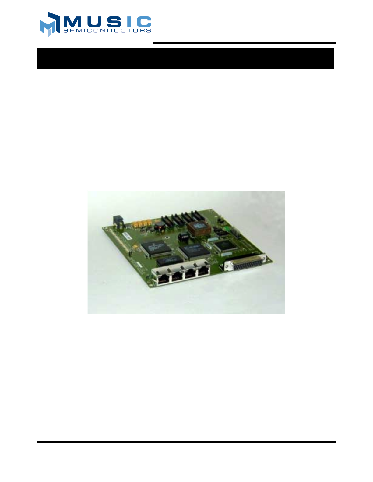
Figure 1: MU9C8338A Evaluation Board
The Evaluation board is shown in Figure 1. It is a very
simple printed circuit board that will allow a user to
evaluate the MUSIC Semiconductors MU9C8338A
Ethernet Filter device. The user simply plugs the board
into a standard PC printer port using the 25-pin connector
supplied. Sample C-Code functions and a demo program
are provided that allows the user to perform the following
tasks:
• Initialize the MU9C8338A and LANCAM
• Read and write internal registers
• Read the LANCAM contents
• Delete LANCAM entries
MUSIC Semiconductors, the MUSIC logo, and the phrase "MUSIC Semiconductors" are May 1, 2001 Rev. 0.2 Draft
Registered tr ademarks of MUSIC Semiconductors. MUSIC is a trademark of
MUSIC Semiconductors.
• Write permanent entries to the LANCAM
• Invoke the Purge routine using the software registers
or INCR pin
• View the data recently transmitted from the hardware
Result Port or Tag port
A simple Windows Software Tool is also provided that
allows the user to view instantly the contents of the
LANCAM database. This tool is called the CAMView
LANCAM Viewer and allows the user to view all or some
of the entries in the device. This can be used in
conjunction with the users own C-Code to play with the
MU9C8338A and view the additions and modifications to
the LANCAM database.
Page 2

MU9C8338A Evaluation Kit Users Manual Hardware Installation
The user may also view any of the device signals by
connecting a logic analyzer to the board. Four
MICTOR-38 high-density connectors are provided that
will allow the user access to the signals. The connectors
are widely used by many logic analyzer pods. Network
traffic can be received by the MU9C8338A through the
RJ-45 connector shown in Figure 2. This enables the user
to send packets and then observe how the device parses
and deals with the Ethernet address information.
HARDWARE INSTALLATION
The Evaluation board is installed in the following way:
1. Remove the power supply unit and cable from the box.
Plug the power supply cable into the power supply unit.
The other end of the cable can be plugged into a
standard 110V outlet. Don’t plug the output connector
into the Evaluation Board for the moment.
2. Remove the 25-pin D-type parallel port connector from
the box. Insert one end into the parallel port connector
in the back of the PC. The board should work with all
parallel port configurations. It shouldn’t matter whether
the port is configured as PS-2, EPP or ECP. The only
stipulation is that the port is capable of bi-directional
data transfer. The base address of the port being used
should be set in any C-Code.
3. Carefully remove the Evaluation board from the
anti-static bag and place on an anti-static surface. It is
advisable that the Evaluation board is used in a lab
environment, where the board can be placed on an
anti-static surface on a work-bench. If this is not
possible, it is important that the board is laid flat on a
desk or table. It is very important that metal objects
should be kept away from the board as they may cause
short circuits in the metal circuit tracks. The board is
supplied with rubber insulating feet applied to the
bottom. These may be removed by hand if the user
wished to lie the board completely flat.
4. Make sure the FPGA data PROM is correctly installed
in socket U10 (see Figure 2 for location).
5. Plug the other end of the parallel port connector into P1
(see Figure 2 for location).
6. Connect the other end of the power supply unit into the
connector J1 (see Figure 2 for location).
7. If the power supply unit is plugged in correctly at the
power socket, two green LEDs D24 and D25 should
now be lit and the red D1 should be flashing (see Figure
2 for location).
8. If D1 is not flashing remove the power cord from J1
and check the data PROM in located properly in socket
U10. If neither of the green LEDs D24 and D25 is lit,
unplug the power supply cord and test the output with
an electrical meter. The output should be approximately
5v DC.
9. If you are still having problems installing the board,
please call MUSIC Semiconductors.
10.When the power is applied, the Result and Tag port
LEDs (see Figure 2 for location) should perform a
self-test and flash a few times. This will allow you to
check that all these LEDs are operational. The LED
self-test jumper (JP9) must be closed or the LEDs will
remain off.
11.If there was no problems, the LEDs should be lit as
described earlier, and you are now ready to use the
Evaluation board. Instructions about how the C-Code
and the Windows Software Tool is installed can be
found in the Software Installation section.
SOFTWARE INSTALLATION
The Evaluation board is supplied with some sample
C-Code, a Windows Software tool, documentation and
some design information. The design information is the
schematics, which are provided in Orcad Capture Version
7.2 format, the FPGA files, and the Verilog code for the
FPGA.
The software is provided on a data CD labeled
"MU9C8338A Evaluation Kit". The CD contains two
setup executable files. One will install the CAMView
LANCAM Viewer and the other will install the C-Code,
schematics, FPGA binary files, and associated
documentation. The CAMView Setup.exe file is located in
the CAMView directory. The installation process for the
LANCAM Viewer is described in detail in a separate
manual. This manual is titled "CAMView LANCAM
Viewer User Manual" and should be found in the Kit along
with this manual. The manual will describe how to install
the Windows Software and how it should be used.
The installation process which installs the C-Code,
documentation, and CAD files is as follows:
1. Insert the data CD titled: "MU9C8338A Evaluation
Kit" in the CD drive.
2. Press the Windows START button and select "Run".
Use "Browse" to select the "Setup.exe" file on the CD.
Click "OK". Alternatively use "Windows Explorer" to
locate the "Setup.exe" file from the CD drive. Once it is
located, double click on the icon.
3. An Install window will pop up that has the title
"MU9C8338A Evaluation Kit". Inside this there will be
a smaller "Welcome" window. Press "Next" to
continue.
2 Rev. 0.2 Draft
Page 3
Software Installation MU9C8338A Evaluation Kit Users Manual
4. An Install window will pop up that has the title
"MU9C8338A Evaluation Kit". Inside this there will be
a smaller "Welcome" window. Press "Next" to
continue.
5. A "User Information" window will prompt you for your
name and Company name. Enter this information if not
automatically entered and press "Next".
6. A "Choose Destination Location" window will prompt
you to specify the default directory for all the files that
will be copied to your computer. You can either leave
this directory as the default shown or use the "Browse"
button to specify another. Once you are ready, press
"Next" to continue.
7. A "Select Program Folder" window will inform you
8. A "Start Copying Files" window will prompt you to
press "Next" to start copying files and thus finish the
installation. Press "Next" to continue. This will copy all
of the files to your hard disk.
9. A "Setup Complete" window will inform you that the
installation has finished. Press "Finish" to complete the
setup.
Once the installation is complete the following files should
have been copied to your hard disk. The default for the
<INSTALL_DIR> is C:\MUSICSemi\Hardware. You may
have changed this during the installation process. If it has
been changed, substitute the new home directory where
<INSTALL_DIR> is shown. The files and their paths are
shown in Tables 1 through 5.
that a new program folder will be created. You can
either leave this folder as shown or change the settings.
Once you are ready, press "Next" to continue.
Table 1: C-Code Files
Path Description
<INSTALL_DIR>\C_Code\Filter.h Header file that contains all the register defines and functions
<INSTALL_DIR>\C_Code\Demo.c Demo file that w ill allow the user to perf orm some basic operati ons
<INSTALL_DIR>\C_Code\Skeleton.c File that shows the basic operation of the board
<INSTALL_DIR>\C_Code\Clear.c File that contains a simple Clear Screen function
Table 2: Documentation Files
Path Description
<INSTALL_DIR>\Docs\8338AEval.pdf This Manual
<INSTALL_DIR>\Docs\8338A Data Sheet.pdf The data sheet for the MU9C8338A
<INSTALL_DIR>\Docs\8338Aerrat a.pdf An errata showing some bugs present in the MU9C 8338A
<INSTALL_DIR>\Docs\AN-N38.pdf An Application note showing how to use the MU9 C8338A
<INSTALL_DIR>\Docs\ AN-N34.pdf An Application note showing how to use the MU9C8338A with the
MPC860 processor
Table 3: Schematic Files
Path Description
<INSTALL_DIR>\Schematics\Eval8358V1.2.dsn The Schematics design file
<INSTALL_DIR>\Schematics\Eval8358V1.2.opj The Schematics OPJ file
Rev. 0.2 Draft 3
Page 4
MU9C8338A Evaluation Kit Users Manual Software Installation
Table 4: Verilog Code
Path Description
<INSTALL_DIR>\Verilog\bufg.v Clock buffer file
<INSTALL_DIR>\Verilog\clk.v Clock divider
<INSTALL_DIR>\Verilog\dp_fifo.v FIFO used to store Result port entries
<INSTALL_DIR>\Verilog\epp.v Par allel port interface
<INSTALL_DIR>\Verilog\fstat.v Fifo entry counter
<INSTALL_DIR>\Verilog\led.v LED control for heartbeat, Result port and Tag port LEDs
<INSTALL_DIR>\Verilog\phy.v PHY register serial access interface
<INSTALL_DIR>\Verilog\phy _led.v LED control for the PHY LEDs
<INSTALL_DIR>\Verilog\proc.v The MU9C8338A processor port interf ace
<INSTALL_DIR>\Verilog\reg.v The FPGA internal registers
<INSTALL_DIR>\Verilog\res.v The MU9C8338A Result port interface
<INSTALL_DIR>\Verilog\rst.v The reset circuit
<INSTALL_DIR>\Verilog\tag.v The MU9C8338A Tag port interface
<INSTALL_DIR>\Verilog\tag_fifo.v FIFO used to store Tag port entries
<INSTALL_DIR>\Verilog\top.v The top lev el module that wires all other modules together
<INSTALL_DIR>\Verilog\mu8338Ademo.v The pseudo pad layer
Table 5: FPGA Binary Files
Path Description
<INSTALL_DIR>\FPGA\8338A.ucf The FPGA constraints file
<INSTALL_DIR>\FPG A\8338AV1_0.bit The FPGA binary file used when down-loading the design into the FPGA.
<INSTALL_DIR>\FPGA\8338AV1_0.mcs The FPGA PRO M file. The version number may change with subsequent
<INSTALL_DIR>\FPGA\res_ra m .edn The edn file for the Result port FIFO memory
<INSTALL_DIR>\FPGA\tag_ram.edn The edn file for the Tag port FIFO memory
The version number may change with subsequent releases.
releases.
4 Rev. 0.2 Draft
Page 5
Hardware MU9C8338A Evaluation Kit Users Manual
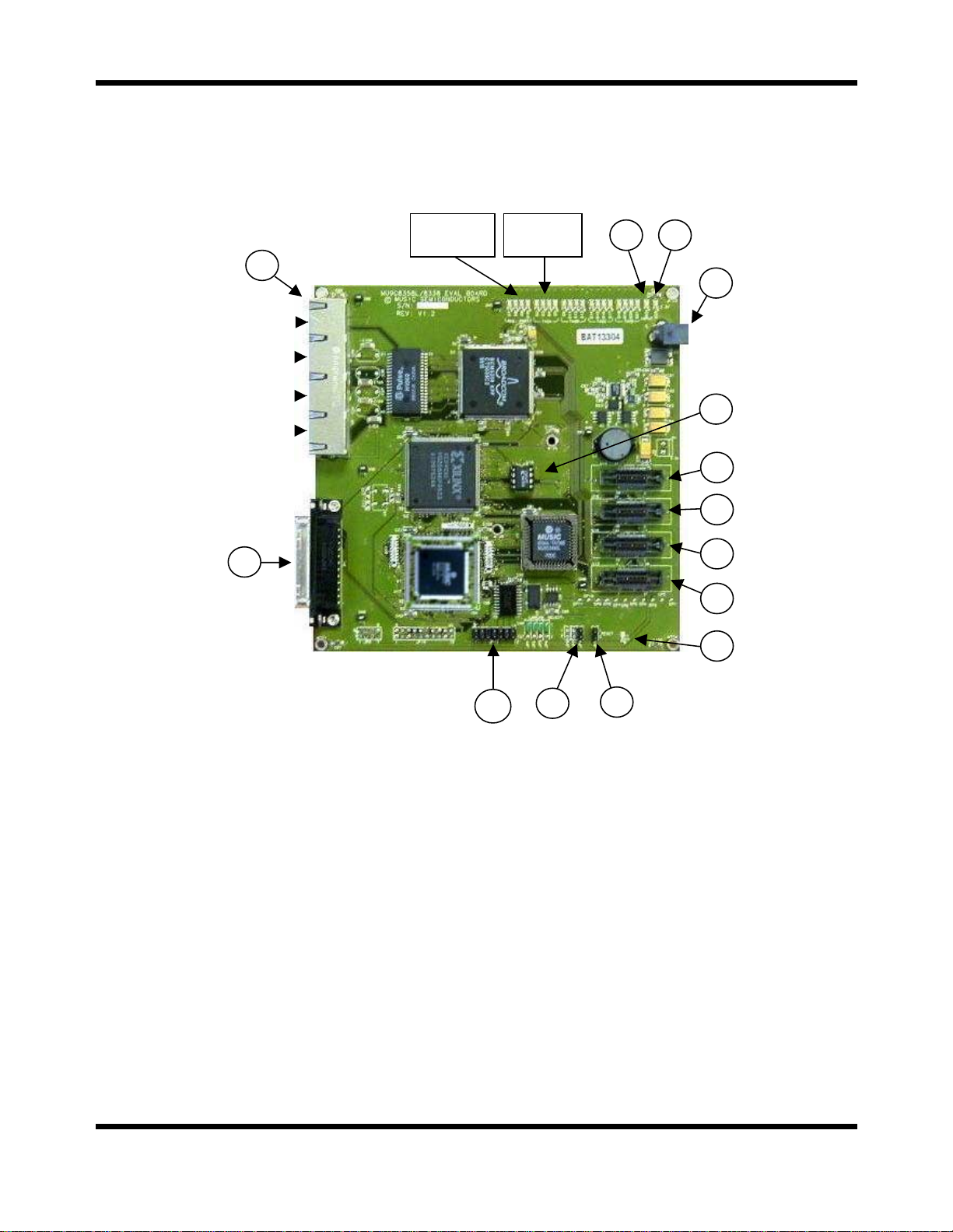
HARDWARE
The Evaluation Board has connectors that allow a logic
analyzer to probe all the signals on the board. There are
also some jumpers that allow the board to be configured or
Result
Port LEDs
U5
10/100 Mb/s
Ethernet Port
Do Not Use
Do Not Use
Do Not Use
P1
reset. LEDs are provided so that the user may quickly
determine the power, FPGA status, Result status, and TAG
port status. Figure 2 shows the location of all these items.
TAG Port
LEDs
D24 D25
J1
U10
U16
U15
U14
Figure 2: Jumper, Connector, and LED Positions
There are four RJ-45 connectors on the board. This is
because the board is also used with the MUSIC
Semiconductors MU9C8358L filter which is a 4-port
device. The user should only connect network traffic to the
port that is shown as "10/100 Mb/s Ethernet" in Figure 2.
Parallel Port
The Evaluation board is connected to a users PC by means
of the Parallel (or printer) port. The Windows GUI and the
C-Code provided assume as default that the Parallel port is
located at address 0x378. The Base Address pre-processor
definition in the Filter.h file may be changed to the address
of your port if it is not 0x378. The Windows GUI will
allow you to choose 0x278 or 0x378 as the Base Address.
If you have problems getting the C-Code or Software GUI
to operate with your Parallel port, please notify MUSIC
Semiconductors.
U13
D1
JP11
JP9
JP5
The Hardware in the Evaluation board is designed in such
a way that it should operate with any parallel port that is
able to perform bi-directional data operations. The
hardware uses the Parallel port in PS-2 mode and expects
the data to be passed using the standard 8-bit Parallel port
data bus. Therefore, it doesn’t matter whether the PC bios
has the port set to Standard, PS-2, EPP or ECP mode as it
should operate in all these modes.
The C-Code routines and the Windows GUI both use the
Standard Parallel port Data and Control registers to output
or input any data. One stipulation is that if the port is set to
ECP mode in the PC bios, the port’s ECR register must be
set to PS-2 mode. The Windows GUI will do this
automatically. Any user specific code must use the
Init_Parallel_Port function as shown in the Skeleton.c file.
This function sets the ECR register appropriately and sets
the control bus to the default values.
Rev. 0.2 Draft 5
Page 6
MU9C8338A Evaluation Kit Users Manual Hardware
WAIT
DATA
ASb
DSb
WRITEb
WAIT
DATA
ASb
DSb
addr[7:0] addr[15:8] data[7:0] data[15:8]
WRITE CYCLES
addr[7:0] addr[15:8] data[7:0] data[15:8]
WRITEb
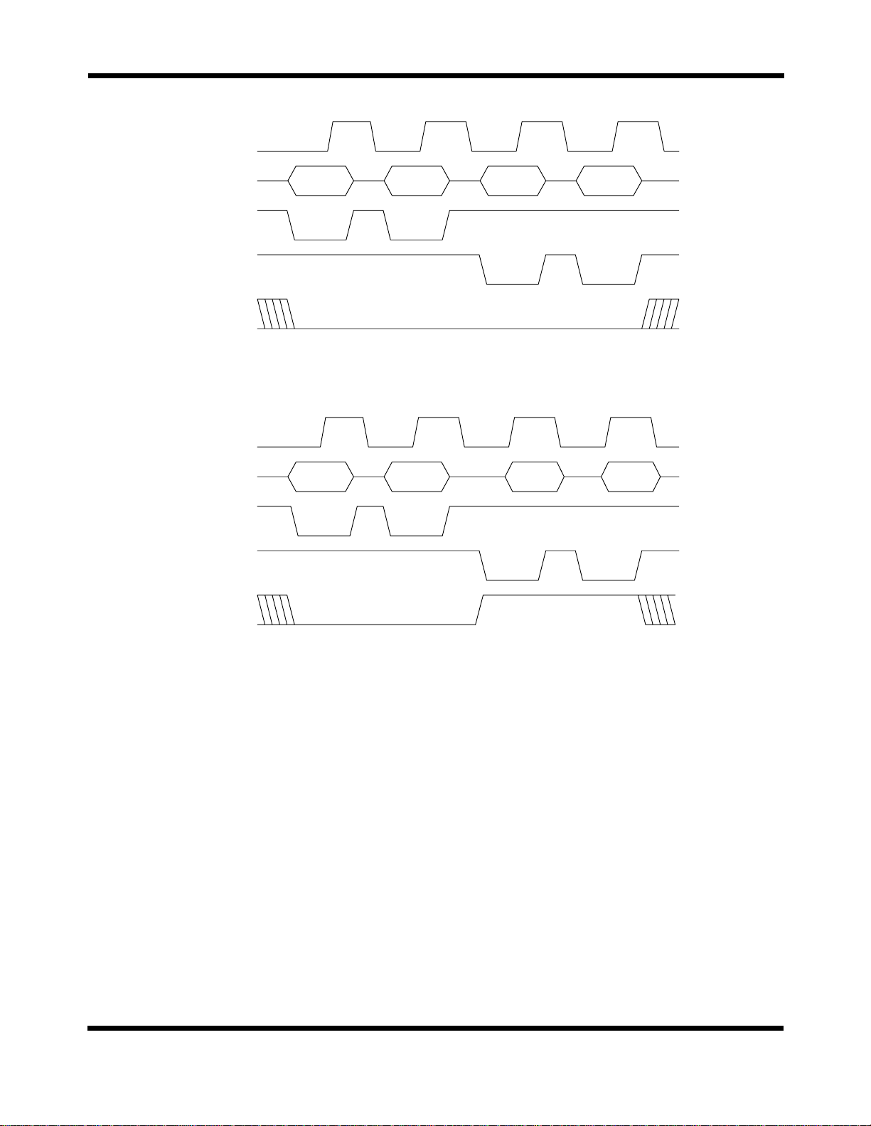
Figure 3: Parallel Port Read and Write Access
The Windows GUI and the C-Code functions transfer data
between the PC and the Evaluation board using four
consecutive 8-bit cycles. This allows a 16-bit address and
a 16-bit data word to be transferred. The FPGA expects a
read and write access to be as it is shown in Figure 3. The
Windows GUI, the reg_write, and reg_read functions use
the Parallel port’s Control register to assert the Address
Strobe (ASb), Data Strobe (DSb), and Write Strobe
(WRITEb) while read or writing the data using the 8-bit
data bus. The GUI and functions also monitor the port’s
Status register to detect the condition of the WAIT signal.
The write access uses two 8-bit address write cycles
followed by two 8-bit data write cycles. The read access
uses two 8-bit address write cycles followed by two 8-bit
data read cycles. Both accesses assert the appropriate
Strobe to indicate where it is an address or data cycle. The
FPGA completes a cycle by asserting its WAIT output.
There is two other Parallel port signals that are not directly
READ CYCLES
used for transferring data. These are the IRQb and INITb
signals. IRQb is a Parallel port input and is asserted low by
the Evaluation board when the MU9C8338A /INTR signal
is asserted low. It will return to its original state, which is
logic 1 once the /INTR output is returned to logic 1. The
user may monitor the state of the IRQb input with the
Poll_For_INTR function or configure their PC to use a
user-designed Interrupt Service Routine. The other signal
is the INITb output, which is used to perform a hardware
reset. The HardWare_Reset function asserts this signal low
to cause a full reset of the Evaluation board.
6 Rev. 0.2 Draft
Page 7

Hardware MU9C8338A Evaluation Kit Users Manual
FPGA Registers
The Evaluation Board has three components that have
internal registers. The three components are the
MU9C8338A Ethernet Filter, the Broadcom Physical
Layer device, and the Xilinx FPGA. All the MU9C8338A
registers that can be read or written are explained in detail
in the MU9C8338A data sheet. The Physical Layer device
internal registers should not normally be altered. The
Evaluation Board is supplied with some basic C-Code that
suit most applications. Neither of these two components
will have their internal registers discussed in this
document.
The Xilinx FPGA allows the user to interface with the
board. It also contains logic that stores Result and Tag data
that was read from the MU9C8338A after it has processed
Ethernet traffic. Table 6 lists all of the registers and gives a
full description.
will allow the Physical Layer device to be configured to
Table 6: FPGA Internal Registers
Address Name R/W Bits Description
00h Revision R [15:8] Version Number. The first versio n is A1.
R [7:0] Revision Number. The first revision is 0.
01h Software Reset R/W [15:0] Write any value to this regis ter or read this r egister to perf o rm a software
reset of the F PGA. Re ading th is re gist er will n ot caus e a re set. Reads as
00h.
02h Result Port Entries
Count
03h Tag Port Entries
Count
04h Reserved R [15:0] This register is not used in this version.
05h Reserved R [15:0] This register is not used in this version.
06h Reserved R [15:0] This register is not used in this version.
07h PHY Read Data R [15:0] When a PHY register is read, the parallel port read cycle completes
08h PHY Status R [15:2] Reads as 0000h.
09h Reserved R [15:0] Thi s register is for MUSIC Semiconductor test purposes .
R [15:4] Reads as 000h.
R [3:0] The number of v al i d entrie s th at are a vailable to be read from th e Resul t
Port FIFO (addr: 14h). The FI FO wil l onl y hold f ifteen entrie s. The Resul t
Port FIFO will only store entries if the Result Port Mode Select register
(addr: 0Ah) is set ap propriately. For a des cription of the Result Port
Hardware, see the Hardware section.
R [15:4] Reads as 000h.
R [3:0] The number of valid entries that are available to be read from the Tag
Port FIFO (addr: 10h). The FIFO will only hold fifteen entries.
For a description of the Tag Port Hardware, see the Hardware section.
before the data is available from the PHY. Therefore, after the register
read is invoked, the data is placed in this register. Any read from the
PHY must be f ol low ed b y a read o f thi s regist er to r etrie v e the dat a. F or a
description of PHY register functions, see the Hardware section.
R [1] 1 = PHY Access in progress.
0 = No PHY access in prog ress.
R [0] 1 = New Read data available in PH Y Read Data register (addr: 07h).
0 = No unread PHY data available.
For a description of PHY register functions, see the Hardware section.
Rev. 0.2 Draft 7
Page 8

MU9C8338A Evaluation Kit Users Manual Hardware
Table 6: FPGA Internal Registers (continued)
Address Name R/W Bits Description
0Ah Result Port
Mode/LED
0Bh INCR Select R/W [15:1] Reads as 0000h.
0Ch – 0Fh Reser ved R [15:0] These regis te r s are no t us e d in t hi s vers io n.
10h Tag Port Data R [15:8] Read as 00h.
11h – 13h Reserved R [15:0] These registers are not used in this version.
14h Result Port Data R [15:0] When the Result Port mode is set to Hardware using the register addr:
R/W [15:5] Reads as 000h.
R/W [4] Heartbeat O n/ O ff.
1 = Heartbeat LED (D1) Off.
0 = Heartbeat LED (D1) flashes to indicate that the FPGA is operating
properly. Default is On.
R/W [3] LED Test. Set this bit to 1 to invoke the LED test. The test will flash the
Result and Tag port LEDs to show that they are all functioning. This is
self-clearing bit and will reset to 0 after the test has been invoked. This
bit will have no effect if the LED test jumper JP 9 is open.
R/W [2] LED On/Off.
1 = The Result and Tag Port LEDs are turned off. The LED test may still
be invoked by setting bit 3.
0 = The Result and Tag P ort LEDs indi cat e ho w man y entrie s are st or ed
in the internal FPGA FIFOs.
R/W [1] Result Port Reset Condition. The RP_SEL and RP_NXT signals should
be held at specific values prior to a hardware reset. Setting this bit to 1,
sets the signals to those values. A hardware reset should be performed
immediately by the user after this bit is set. The bit will clear after the
reset. This is explained further in the Result Port Hardware description
in the Hardware section.
R/W [0] Result Port Mode. The result data can be read from the Result
Hardware p ort or f rom a n int ernal M U9C8 338 A r egist er. If the result po rt
is used to retrieve the data, the FPGA will read the data and store in an
internal FIFO.
0 = Hardware Mode. The RP_SEL and RP_NXT signal s are enabled to
read the port.
1 = Software Mode. The RP_SEL and RP_NXT signals are held at logic
0, thus transferring all results to the MU9C8338A internal register.
R/W [0] Write a 1 to this bit to cause the MU9C8338A INCR in put pin to be
asserted. This is a sel f-clearing bit and will reset to 0 after the pin has
been asserted and de-asserted. The internal MU9C8338A register that
allows the INCR to be enabled must be set appropriately prior to setting
this bit.
R [7] FRX_ER. If this bit is 1, the FRX_ER pin of the Tag port was asserted.
R [6] REJ. If this bit is se t, the REJ pi n wa s ass e rted.
R [5:0] The Tag port Port ID data. I f no Port ID was i dentified, 3Fh is given as
the Port ID.
The number of entries available will be indicated in the Tag Port Entries
Count register (addr: 03h) and also shown by the LEDs D2 through D5
(if enabled).
For a description of the Tag Port Hardware, see the Hardware section.
0Fh, the RP_SEL and RP_NXT pins are enabled. Any result data will be
read by the FPGA and pl ac ed in an int erna l FIFO. The data can be read
from this regist er . The numb er of entri es av ail abl e will be in dicat ed in the
Result Port Entries Count register (addr: 02h) and also shown by the
LEDs D7 through D10 (if enabled).
For a description of the Result Port Hardware, see the Hardware
section.
8 Rev. 0.2 Draft
Page 9

Hardware MU9C8338A Evaluation Kit Users Manual
Jumpers
The Evaluation Board has jumper pins that allow the user
to configure options and connect an external JTAG
Controller pod. Table 7 shows the board and where each of
the jumpers or connector is located.
Table 7: Jumper Description
Jumper Name Description
JP5 Reset Short the pins to cause a hardw are r eset of all compo nents on th e Ev aluat ion bo ard. The
JP9 LED Test On/Off Open: The LED tes t is disabled. While this ju mper is open, initiating an LED test from
JP11 JTAG Controll er A JTAG Controller pod may be connected to the board. The JTAG circuitry of the
MU9C8338A, LANC AM, FPGA, and PHY will all be reset.
register 0Fh will hav e no effect.
Closed: The LED t est will be performed on power up, hardware reset and if register 0Fh
bit 3 is set to 1.
MU9C8338A and PHY is connected to the pod to allow the user to evaluate the
MU9C8338A’s JT AG functions. If thi s is not required, leave the connector open.
Pin 1 – TMS
Pin 2 – TRST
Pin 3 – TDI
Pin 4 – 0v
Pin 5 – Unconnected
Pin 6 – No pin for keying
Pin 7 – TDO
Pin 8 – 0v
Pin 9 – TCK Return
Pin 10 – 0v
Pin 11 – TCK
Pin 12 – 0v
Pin 13 – Unconnected
Pin 14 – Unconnected
Rev. 0.2 Draft 9
Page 10

MU9C8338A Evaluation Kit Users Manual Hardware
Logic Analyzer P ort
The Evaluation board has 4 logic analyzer pods. These
allow a "MICTOR-38" style connector to be used to probe
any of the internal signals. The positions of the connectors
are shown in Figure 1. Tables 8 through 11 list each of the
signals that are available for probing.
Table 8: Logic Analyzer Pod U13
Pod U13
Pin 38 D0 MII RX CLK Pin 37 D0 Not Used (see note)
Pin 36 D1 MII RX ER Pin 35 D1 Not Used (see note)
Pin 34 D2 MII RX D3 Pin 33 D2 Not Used (see note)
Pin 32 D3 MII RX D2 Pin 31 D3 Not Used (see note)
Pin 30 D4 MII RX D1 Pin 29 D4 Not Used (see note)
Pin 28 D5 MII RX D0 Pin 27 D5 Not Used (see note)
Pin 26 D6 MII RX DV Pin 25 D6 Not Used (see note)
Pin 24 D7 MII RX COL Pin 23 D7 Not Used (see note)
Pin 22 D8 MII RX CRS Pin 21 D8 Not Used (see note)
Pin 20 D9 Not Used (see note) Pin 19 D9 Not Used (see note)
Pin 18 D10 Not Used (see note) Pin 17 D10 Not Used (see note)
Pin 16 D11 Not Used (see note) Pin 15 D11 RP_SEL
Pin 14 D12 Not Used (see note) Pin 13 D12 RP_NXT
Pin 12 D13 Not Used (see note) Pin 11 D13 RP_DV
Pin 10 D14 Not Used (see note) Pin 9 D14 Hardware Reset (/Reset)
Pin 8 D15 Not Used (see note) Pin 7 D15 NC
Pin 6 CLK System 50MHz Clock Pin 5 CLK System 50MHz Clock
Pin 4 GND 0v Pin 3 SDA NC
Pin 2 +5v NC Pin 1 SCL NC
Table 9: Logic Analyzer Pod U14
Pod U14
Pin 38 D0 Not Used (see note) Pin 37 D0 Tag port REJ
Pin 36 D1 Not Used (see note) Pin 35 D1 Not Used (see note)
Pin 34 D2 Not Used (see note) Pin 33 D2 Not Used (see note)
Pin 32 D3 Not Used (see note) Pin 31 D3 Not Used (see note)
Pin 30 D4 Not Used (see note) Pin 29 D4 Tag port FRX_ER
Pin 28 D5 Not Used (see note) Pin 27 D5 Not Used (see note)
Pin 26 D6 Not Used (see note) Pin 25 D6 Not Used (see note)
Pin 24 D7 Not Used (see note) Pin 23 D7 Not Used (see note)
Pin 22 D8 Not Used (see note) Pin 21 D8 Tag port TP_SD
Pin 20 D9 LANCAM /E Pin 19 D9 Not Used (see note)
Pin 18 D10 LANCAM /W Pin 17 D10 Not Used (see note)
Pin 16 D11 LANCAM /CM Pin 15 D11 Not Used (see note)
Pin 14 D12 LANCAM /EC Pin 13 D12 Tag port TP_DV
Pin 12 D13 LANCAM /MI Pin 1 1 D13 Not Used (see note)
Pin 10 D14 LANCAM /FI Pin 9 D14 Not Used (see note)
Pin 8 D15 LANCAM /RESET_LC Pin 7 D15 Not Used (see note)
Pin 6 CLK System 50MHz Clock Pin 5 CLK System 50MHz Clock
Pin 4 GND 0v Pin 3 SDA NC
Pin 2 +5v NC Pin 1 SCL NC
10 Rev. 0.2 Draft
Page 11

Hardware MU9C8338A Evaluation Kit Users Manual
Table 10: Logic Analyzer Pod U15
Pod U15
Pin 38 D0 D0 Pin 37 D0 /PCS
Pin 36 D1 D1 Pin 35 D1 /PCSS
Pin 34 D2 D2 Pin 33 D2 /WRITE
Pin 32 D3 D3 Pin 31 D3 PROC_RDY
Pin 30 D4 D4 Pin 29 D4 /INTR
Pin 28 D5 D5 Pin 27 D5 INCR
Pin 26 D6 D6 Pin 25 D6 PHY MDC
Pin 24 D7 D7 Pin 23 D7 PHY MDIO
Pin 22 D8 D8 Pin 21 D8 A0
Pin 20 D9 D9 Pin 19 D9 A1
Pin 18 D10 D10 Pin 17 D10 A2
Pin 16 D11 D11 Pin 15 D11 A3
Pin 14 D12 D12 Pin 13 D12 A4
Pin 12 D13 D13 Pin 11 D13 A5
Pin 10 D14 D14 Pin 9 D14 A6
Pin 8 D15 D15 Pin 7 D15 A7
Pin 6 CLK System 50MHz Clock Pin 5 CLK System 50MHz Clock
Pin 4 GND 0v Pin 3 SDA NC
Pin 2 +5v NC Pin 1 SCL NC
Table 11: Logic Analyzer Pod U16
Pod U16
Pin 38 D0 RP0 Pin 37 D0 LANCAM DQ0
Pin 36 D1 RP1 Pin 35 D1 LANCAM DQ1
Pin 34 D2 RP2 Pin 33 D2 LANCAM DQ2
Pin 32 D3 RP3 Pin 31 D3 LANCAM DQ3
Pin 30 D4 RP4 Pin 29 D4 LANCAM DQ4
Pin 28 D5 RP5 Pin 27 D5 LANCAM DQ5
Pin 26 D6 RP6 Pin 25 D6 LANCAM DQ6
Pin 24 D7 RP7 Pin 23 D7 LANCAM DQ7
Pin 22 D8 RP8 Pin 21 D8 LANCAM DQ8
Pin 20 D9 RP9 Pin 19 D9 LANCAM DQ9
Pin 18 D10 RP10 Pin 17 D10 LANCAM DQ10
Pin 16 D11 RP11 Pin 15 D11 LANCAM DQ11
Pin 14 D12 RP12 Pin 13 D12 LANCAM DQ12
Pin 12 D13 RP13 Pin 11 D13 LANCAM DQ13
Pin 10 D14 RP14 Pin 9 D14 LANCAM DQ14
Pin 8 D15 RP15 Pin 7 D15 LANCAM DQ15
Pin 6 CLK System 50MHz Clock Pin 5 CLK System 50MHz Clock
Pin 4 GND 0v Pin 3 SDA NC
Pin 2 +5v NC Pin 1 SCL NC
Note: NC = No Connect. “Not Used” indicates a pin that was used in the MU9C8358L version of the Evaluation board but is not used
here.
Rev. 0.2 Draft 11
Page 12

MU9C8338A Evaluation Kit Users Manual Hardware
LEDs
The Evaluation board has diagnostic LEDs. Figure 2
shows the position of the LEDs that indicate the power,
and FPGA heartbeat status. There are also eight LEDs that
indicate the number of unread Result and Tag port entries
that reside in the FPGA FIFOs. These are marked on the
Bit 0
Bit 1
Bit 2
Bit 3
Bit 3
Bit 2
Bit 1
Bit 0
Figure 4: Result and Tag Port LEDs
Figure 4 shows more clearly the Tag port and Result port
LEDs which indicate the number of valid entries in the
corresponding FIFO. Each of the sets of LEDs operates in
the same way. That is that each LED will be on or off to
show the number of entries as a 4-bit binary value. This
can be seen in Figure 4. Therefore, if D5 and D3 were on
and D2 and D4 were off, the FIFO for the Tag port would
have 5 entries available.
Figure 5 shows the position of the LED that indicates the
LINK status for the Ethernet port. It also shows the LED,
which indicates that the Ethernet port is receiving data.
board as RES PORT and TAGA. The LEDs marked as
TAGB, TAGC, and TAGD were used in the MU9C8358L
version of this board and will normally remain off. The
position of the LEDs is shown in Figure 2 and also shown
in Figure 4.
Unused
The LINK LED will illuminate green when the LINK is
good and be off when there is no LINK. The Receive LED
will illuminate red when the port is receiving data and be
off when it is not. All of the LEDs found on the Evaluation
Board are explained in Table 12.
The Evaluation board has four RJ-45 connectors on it.
Only the connector indicated as the Ethernet port in Figure
5 should be used. The remaining three connectors should
be left open as these are not connected to the
MU9C8338A. These are used in the MU9C8358L version
of this board, which has four Ethernet ports.
Receive
LED
LINK
LED
Figure 5: Receive and LINK Status LEDs
12 Rev. 0.2 Draft
Page 13

Hardware MU9C8338A Evaluation Kit Users Manual
Table 12: Evaluation Board LEDs
LED Name Description
D1 Heartbeat This LED will fl ash if the FPGA is functioning pr operly. After power-up, this LED should
D7,
D8,
D9,
D10
D2,
D3,
D4,
D5
D6,
D11,
D12,
D13
D14,
D15,
D16,
D17
D18,
D19,
D20,
D21
D24 Input Supply This LED indicates that the power supply uni t is operating cor rectly.
D25 3.3v Supply This LE D indicates that the Evaluation board has a 3.3v power supply.
A-Right Link LED This LED is found on the RJ-45 connector. The Ethernet port has an LED to indicate LINK
A-Left Receive LED This LED is f ou nd o n the R J-45 conn ect or. The Ethernet port has an LED to indi cate t ha t the
Result Port Data Count These four LEDs indicate how many results are in the internal FPGA FIFO. The FIFO will
Tag Port Data Count These four LEDs indicate how many entries are in the internal Tag Port FIFO. The FIFO will
Not used These LED s were used on the MU 9C8358L version of the Evaluation board. They will flash
Not Used These LEDs were used on the MU9C8358L version of the Evaluation board. They will f lash
Not Used These LEDs were used on the MU9C8358L version of the Evaluation board. They will f lash
alwa ys b e fl ashi ng . If i t i s no t, the F PGA b it P R OM ( U10) or F PGA ( U7) may be faulty. Please
verify if U10 is in place and FPGA register 0Fh bit 4 = 0.
After power-up, setting bit 4 of the FPGA register 0Fh to 1 will turn off this LED.
store up to fif t een resu lt s r ead f rom t he MU9C 8338A Re sul t Port. The LEDs repr e sen t a 4-b it
value in order to show how many entries are available. The LEDs are decoded as follows:
D7 = bit 3 (msb)
D8 = bit 2
D9 = bit 1
D10 = bit 0 (lsb)
After power-up, setting bit 2 of the FPGA register 0Fh to 1 will turn off these LEDs .
store up to fifteen entries read from the MU9C8338A Tag Port. The LEDs represent a 4-bit
value in order to show how many entries are available. The LEDs are decoded as follows:
D2 = bit 3 (msb)
D3 = bit 2
D4 = bit 1
D5 = bit 0 (lsb)
After power-up, setting bit 2 of the FPGA register 0Fh to 1 will turn off these LEDs .
during power-up and during any LED tests. They will remain off in normal operation.
during power-up and during any LED tests. They will remain off in normal operation.
during power-up and during any LED tests. They will remain off in normal operation.
status. If LINK is good, the GREEN LED is on. As you look at th e front of the RJ-45
connector, the LINK LED is in the top right corner . This is shown in Figure 5.
Evaluation board is receiving network traffic. If the board is receiving packets, the Ethernet
port’s RED LE D is f l ashi ng . As you look at the front of t he RJ- 45 c onn ecto r, the Receive LE D
is in the top left corner. This is shown in Figure 5.
Result Port Hardware
The MU9C8338A has a Hardware Result port that allows
the user to read the results of the Source and Destination
address searches as they are processed. The Hardware port
is directly connected to the Xilinx FPGA. This allows the
board to read out the result data, as it becomes available
and store it in an internal FIFO within the FPGA. The
FPGA asserts the RP_SEL and RP_NXT signals as it is
described in the MU9C8338A data sheet. This transfers
the results from the MU9C8338A to the FPGA FIFO.
The FIFO is capable of storing up to fifteen results. An
internal FPGA register indicates how many valid FIFO
entries are available. The number of entries is also
indicated by means of four LEDs, which gives the user a
Rev. 0.2 Draft 13
visual indication when there is valid data to be read. The
LEDs can be turned on or off by setting bit 2 of the Result
Port Mode/LED register to 1 (off) or 0 (on).
The MU9C8338A also has the Result Data (RDAT)
software register which stores results, as they become
available. The Result Status (RSTAT) register indicates if
there is a valid result to be read from the RDAT register.
The RDAT register will only store results when the
Hardware port is not being used. The Evaluation board
regards the Result Hardware port as "not being used"
when the FPGA ignores the RP_DV assertion when a
result is available. Under this circumstance, all valid
results are only available through the MU9C8338A RDAT
register.
Page 14

MU9C8338A Evaluation Kit Users Manual Hardware
The user must configure the Evaluation board to operate
its Result Port accesses in Software mode or Hardware
mode. The data is available in chronological order in
either mode. This means that the result that was
transferred first is read first. Once the FIFO is full,
subsequent results will be read from the Result port but
from the FIFO. The user is able to inspect the Hardware
Result port by connecting a logic analyzer to the board’s
logic analyzer connectors U13 and U16. The two modes
are described in Table 13. Table 14 shows the data register,
count register, and the LEDs that display the number of
entries in the Result port FIFO.
discarded. This will continue until entries have been read
Table 13: Result Port Mode
Mode Configuration Description
Hardware Set Result Port Mode/LED (0Fh) r egister bit 0 to 0.
This is the default setting.
Software Set Result Port Mode/LED (0Fh) register bit 0 to 1. The result data is only available through the MU9C8338A software
The result d ata is au tomat ical ly re ad by the FP GA and placed in th e
Result FIFO. Reading the Result Port Data (09h) register can
access this da ta. Reading the Result Port Entries Count (02h)
register can identify the number of valid entries. The Result Port
LEDs D7 through D10 also indicates the number of entries.
register. The Result Port signals RP_SEL and RP_NXT are held at
logic 0. The Result Port LEDs D7 through D10 are turned off in
software mode.
Table 14: Result Port Count LEDs
Count LEDs
Port Data Register Count Register Bit 3 Bit 2 Bit 1 Bit 0
Result 09h 02h D7 D8 D9 D10
Tag Port Hardware
The MU9C8338A has a Tag port, which transfers the Tag
ID to systems, which support Tag Switching. The Tag port
is directly connected to the Xilinx FPGA. This allows the
board to read Tag data, as it becomes available and store it
in an internal FIFO within the FPGA. The FIFO is capable
of storing up to fifteen Tag IDs. An internal FPGA register
indicates how many valid FIFO entries are available. The
number of entries is also indicated by means of four LEDs,
which gives the user a visual indication when there is valid
data to be read.
The data is available in chronological order, which means
that the ID that was transferred first is read first. Once the
FIFO is full, subsequent Tag IDs will be discarded and not
stored in the FIFO. This will continue until entries have
been read from the FIFO. The user is able to inspect the
Tag port by connecting a logic analyzer to the board’s
logic analyzer connector U14. Table 15 shows how the
Tag information is stored in the FPGA FIFO. Table 16
shows the data register, count register, and the LEDs that
display the number of entries. The LEDs can be turned on
or off by setting bit 2 of the Result Port Mode/LED
register (0Fh) to 1 (off) or 0 (on).
Table 15: Tag Port Data Stored in FPGA FIFO
Bit Name Description
[15:8] Reserved Read as 0.
[7] FRX_ER If this bit is 1, the FRX_ER pin of the Tag port was asserted.
[6] REJECT If this bit is set, the REJ pin was asserted.
[5:0] Port ID The Port ID data which indicates to which physical port the Ethernet packet should be
forwarded. If no Port ID was identified, 3Fh is given as the Port ID.
Table 16: Tag Port Count LEDs
Count LEDs
Port Data Register Count Register Bit 3 Bit 2 Bit 1 Bit 0
Tag 0Ah 03h D2 D3 D4 D5
14 Rev. 0.2 Draft
Page 15

Hardware MU9C8338A Evaluation Kit Users Manual
C-Code
The Evaluation kit is supplied with four C-Code files,
which allows the user to evaluate the MU9C8338A. The
four files and a description of their use is as follows:
• Filter.h
This file contains the Evaluation board C-Code functions, pre-processor defines and the initialization data
structure.
• Demo.c
This file contains a C-Code program that shows the
basic operations of the Evaluation board. It also contains some functions used to display the data to the
screen.
•Skelton.c
This file contains a C-Code program that shows the
minimum initialization.
• Clear.c
This file contains a C-Code function that will clear the
PC Screen for use in Demo.c.
Using the C-Code
The four files can be used with most C Compliers. The
Demo.c file uses a function called Cls. This function is
found the Clear.c file and uses some Windows built-in
routines to clear the PC screen. If you are using a
non-Windows C compiler or your compiler is not
compatible with the function, the Cls function should be
removed from the Demo.c and Filter.h files. Removing the
following pre-processor code from the Demo.c file will
disable the Cls function:
#define CLS_ON 1
The procedure for using the Skeleton.c and Demo.c files is
as follows:
Demo.c
1. Place the Demo.c, Clear.c and Filter.h files in the same
directory.
2. Compile and build the Demo.c file.
3. Run the resulting executable.
Skeleton.c
1. Place the Skeleton.c and Filter.h files in the same
directory.
2. The Skeleton.c file shows the minimum initialization
that should be performed. The user should add their
own code to this file. The functions found in Filter.h
may be used or the user may use their own as long as
the register accesses follow the same method shown in
reg_write and reg_read.
3. Compile and build the Skeleton.c file
4. Run the resulting executable.
5. When using your C-Code, you can also use the
CAMView Windows GUI in parallel. This will allow
you to view the LANCAM contents.
Register Access
The C-Code is supplied with two functions to read and
write the internal registers of the MU9C8338A and the
interface FPGA. The functions are reg_read and reg_write
and are described in Table 21. They have a 16-bit input
parameter to specify the address of the register to be
accessed. All of the registers that can normally be written
to or read from are shown in Tables 17 through 19 along
with the input parameter that should be used. The PHY
registers are not shown, as the user would not normally
directly access them. The register pre-processor values are
defined in the Filter.h file and should be accessed as
shown in the following two examples:
reg_write(STARG, 0x0C);
U16 read_data = reg_read(SSTAT);
Data can written to or read from the Evaluation board
registers directly as shown above. They can also be
accessed indirectly by setting the members of the
Initialization data structure followed by using the
Init_8338A_LANCAM or Init_PHY functions. Tables 17
through 19 shows also the data structure member that
should be set if the register has one associated with it. An
example of how this would be used is shown in the Data
Structure section.
4. A banner message should be displayed. Follow the
instructions and you should be able to view entries, add
entries, delete entries, purge entries, view Result and
Tag port data.
5. If the Cls function used is not compatible with your
compiler comment out the following line from the
beginning of Demo.c: #define CLS_ON 1
6. When using the C-Code, you can also use the
CAMView Windows GUI in parallel. This will allow
you to view the LANCAM contents.
Rev. 0.2 Draft 15
Page 16

MU9C8338A Evaluation Kit Users Manual Hardware
Table 17: MU9C8338A System Register Address Parameter Names
Register Name Evaluation Board
Address
System Status 0x0100 SSTAT
System Static Configuration 0x0101 SSCFG_Reg SSCFG
System Dynamic Configuration 0x0102 SDCFG
System Target 0x0103 STARG_Reg STARG
System CAM Data Word 0 0x0105 SCDW0
System CAM Data Word 1 0x0106 SCDW1
System CAM Data Word 2 0x0107 SCDW2
System CAM Data Word 3 0x0108 SCDW3
System Time-stam p Purge 0x0109 STPU RG
System Time-stam p Curre nt 0x010A STCURR
System Max SA/DA Cycles 0x010C SMXSADACYC_Reg SMXSADACYC
System Status Word B 0x010D SCSWB
System Status Word A 0x010E SCSWA
System SA Update 0x0110 SSAU
System SA Learn 0x0111 SSAL
System LANCAM Control 0x0112 SLCC S
System Command (delete) 0x0120 SDO_DELETE
System Command (add) 0x0121 SDO_ADD
System Command (read) 0x0124 SDO_READ
System Command (inc TS) 0x0126 SDO_INCTS
System Command (inc PR) 0x0127 SDO_INCPR
System Command (inc TS+PR) 0x0128 SDO_INCTSPR
System Command (set address) 0x0129 SDO_SETADD
Structure Member Input Parameter
Table 18: MU9C8338A Chip and Po rt Register Address Parameter Names
Register Name Evaluation Board
Address
Chip Role 0x0001 CHIPROL
Chip Version 0x0002 CHIPVER
Result Status 0x0003 RSTAT
Result Data 0x0004 RDAT
Port ID 0x0040 PORT_ID_Reg PID
Port Configure 0x0041 PCFG_Reg PCFG
Port Target 0x0042 PTARG_Reg PTARG
Port Configure Extended 0x0044 PCFG_EXT_Reg PCFG_EXT
Structure Member Register D ef ine
Table 19: FPGA Register Address Parameter Names
Register Name Evaluation
Board Address
Version 0x4000 FPGA_VERSION
Software Reset 0x4001 FPGA_SOFT_RESET
Number of Result P ort Entries 0x4002 FPGA_ RES_PORT_ENTRIES
Number of Tag Port Entries 0x4003 FPGA_TAG_ENTRIES
PHY Read Data 0x4007 FPGA_PHY_DATA
PHY Read Data Valid 0x4008 FPGA_PHY_DATA_VALID
Result Por t Data 0x4009 FPGA_RES_PORT_DATA
Tag Port Data 0x400A FPGA_TAG_DATA
Result Port Mode / LED Control 0x400F FPGA_RESULT_SEL
INCR Pin Assert 0x4010 FP GA_ INC R_INVOKE
Register Define
16 Rev. 0.2 Draft
Page 17

Hardware MU9C8338A Evaluation Kit Users Manual
Functions
The Filter.c file contains functions that can be used to
perform standard operations on the Evaluation board.
Tables 20 through 24 describe each of the functions.
Table 20: Low Level Parallel Port Access
Function Input Parameters Return Value Description
Address_Cycle U8 addr – the 8-bit data value
placed on th e par all el port dat a b us
during a parallel port address cycle
Data_Write_Cycle U8 data – the 8-bit data val ue
placed on th e par all el port dat a b us
during a parall el port write data
cycle
Data_Read_Cyc le None U8 - the 8-b it d ata value read from
Poll_For_INTR None U8 – Indicates state of /INTR
None This low l ev el func tion writes an 8-bit
None This low l ev el func tion writes an 8-bit
the parall el port data bus during a
parallel port read data cycle
output. The two possibilities are:
INTR_HIGH or INTR_LOW
value and asse rts the pa rallel port
signals appropriately
value and asse rts the pa rallel port
signals appropriately
This low l ev el funct ion read s an 8- bit
value and asse rts the pa rallel port
signals appropriately
This low level function will check the
state of the Parallel port IRQb
output, whic h in turn indic at es the
state of the MU9C8338A /INTR
output.
Table 21: Register Access
Function Input Parameters Return Value Description
reg_write U16 addr – the 16-bit address of
the register to be written to. This
can be any of the writ ab le 8338A or
FPGA registers defined in Filter.h
U16 data – the 16 - b it da ta to be
written.
reg_read U16 addr – the 16-bit address of
the register t o be read. Th is ca n be
any of the readable 8338A or
FPGA registers defined in Filter.h
None This function uses the low-level
U16 data – the 16-bit data read
from the register.
parallel port functions to write to a
register on the Eval uation boar d (not
the PHY).
This function uses the low-lev e l
parallel po rt functions to read fro m a
register on the Eval uation boar d (not
the PHY).
Table 22: PHY Register Access
Function Input Parameters Return Value Description
PHY_reg_write U16 addr – the 16-bi t address of
the PHY register to be written to.
U16 data – the 16 - b it da ta to be
written.
PHY_reg_read U16 addr – the 16-bit address of
the register to be read.
None This function uses the low-level
U16 data – the 16-bit data read
from the register.
parallel port functions to write to a
PHY register.
This function uses the low-lev e l
parallel po rt functions to read fro m a
PHY register.
Rev. 0.2 Draft 17
Page 18

MU9C8338A Evaluation Kit Users Manual Hardware
Table 23: LANCAM Access
Function Input Parameters Return Value Description
Command_Write U16 data – the 16-bit data to be
written during the Command Write.
Command_Read None U16 – the 16-bit data that is read
Data_Write U16 data – the 16-bit data to b e
written during the Data Write.
None This function uses the SCDW0 and
SLCCS registers to perform a
LANCAM Command Write.
This function uses the SCDW0 and
from the LANCAM during the
Command Read.
None This function uses the SCDW0 and
SLCCS registers to perform a
LANCAM Command Read. This
function uses a special register in
the FPGA as the 8338A does not
allow you to read individual
LANCAM registers.
SLCCS registers to perform a
LANCAM Data Write.
Table 24: Initialization
Function Input Parameters Return Value Description
Init_8338A_LANCAM Init_t *pInit – a pointer to an
initialization data structure. The
structure specifies the values to
be written to the 83 38A r egister s.
Init_PHY Init_t *pInit – a pointer to an
initialization data structure. The
structure specifies the values to
be written to the PHY control
register.
Init_P aral lel_ P ort None Non e This function sets the EC R regis ter
HardWare_Reset None None This function performs a hardware
Display_Ban ner U16 FPGA_VER – th e 16 -b it
version register value read from
the FPGA.
U16 FILTER_VER – the 16-bit
version register value read from
the 8338A.
None This function initializes the 8338A
and the LANCAM the same way as
it is described in Application Note
ANN-38.
U16 – returns whet her the
Initialization is successful or not.
None This function will display a banner
This function initiali zes the PHY to
be Full or Half Duplex,
Auto-negotiating, 10Mb/s or
100Mb/s.
to PS2 mode and sets the parallel
port signals to the default
condition.
reset by asserting the Reset inputs
of the FPGA, PHY, 8338A and
LANCAM.
that shows t he version of the
8338A and FPGA being used.
18 Rev. 0.2 Draft
Page 19

Hardware MU9C8338A Evaluation Kit Users Manual
Initialization Data Structure
The C-Code uses a data structure to store Initialization
information. The normal procedure would be to set the
structure to some initialization functions. The data structure
is found in the Filter.h file and is shown in Figure 6.
members to the appropriate values and pass a pointer to the
typedef struct {
/*System Registers*/
U16 SSCFG_Reg;
U16 STARG_Reg;
U16 SMXSADACYC_Reg;
/*Port Registers*/
U16 PCFG_Reg;
U16 PORT_ID_Reg;
U16 PTARG_Reg;
U16 PCFG_EXT_Reg;
/*Phy Initialization Regs*/
U16 MIIControl_Reg;
} Init_t;
Figure 6: Initialization Data Structure
The initialization functions are Init_8338A_LANCAM
and Init_PHY. The MU9C8338A register data members
should be set to the values shown in the device data sheet.
The PHY register data members should be set to either of
port to be Full or Half Duplex. It will also set the speed to
be fixed as 10Mb/s or 100Mb/s or to auto-negotiate. An
example of how the data structure should be used for both
initialization functions is shown in Figures 7 and 8.
the values shown in Table 25. This will initialize the PHY
Table 25: PHY Register Initialization Values
PHY Register Value Full Duplex Half Duplex Auto-negotiate 10Mb/s 100Mb/s
FULL_DUPLEX_AUTO_NEG Yes No Yes No No
FULL_DUPLEX_10Mb Yes N o No Yes N o
FULL_DUPLEX_100Mb Ye s No No No Ye s
HALF_DUPLEX_AUTO_NEG No Yes Yes No No
HALF_DUPLEX_10Mb No Yes No Yes No
HALF_DUPLEX_100Mb No Yes No No Yes
Rev. 0.2 Draft 19
Page 20

MU9C8338A Evaluation Kit Users Manual Hardware
Init_t Init_St;
Init_St.SSCFG_Reg = 0x04; /* 70 ns LANCAM, active high reject*/
Init_St.STARG_Reg = 0x0C; /* INCR enabled,
/FI interrupt disabled */
Init_St.SMXSADACYC_Reg = 0x20; /* 70 ns LANCAM */
Init_St.PCFG_Reg = 0x0; /* Disable CRC Check */
Init_St.PORT_ID_Reg = 0x20;
Init_St.PTARG_Reg = 0x50; /* DA processed, SA processed */
Init_St.PCFG_EXT_Reg = 0x06; /* Multicast DA processed, SA processed */
Init_8338A_LANCAM
(&Init_St);
Figure 7: Use of Initialization Data Structure with Init_8338A_LANCAM
Init_t Init_St;
Init _S t .MIIContr olA_Reg = FU L L _DUPLEX_A U TO _NEG;
Init_PHY(&Init_St);
Figure 8: Use of Initialization Data Structure with Init_PHY
MUSIC Semiconductors’ agent or distributor:
Worldwide Headquarters
MUSIC Semiconductors
1521 California Circ le
Milpitas, CA 95035
USA
Tel: 408 869-4600
Fax: 408 942-0837
http://www.musicsemi.com
email: info@musicsemi .com
USA Only: 800 933-1550 Tech Support
888 226-6874 Product Info
MUSIC Semiconductors reserves the right to make changes to its products and
specifications at any time in order to improve on performance, manufacturability or
reliability. Information furnished by MUSIC is believed to be accurate, but no
responsibilit y is assu med by MUSI C Se micon du ctors for th e use of said i nforma tion , nor
for any infringements of patents or of other third -par ty righ ts whic h may result from said
use. No license is granted by implication or otherwise under any patent or patent rights of
any MUSIC comp any.
© Copyright 2001, M USIC Semiconductors
Asian Headquarters
MUSIC Semiconductors
Special Export Processing Zone
Carmelray I ndustrial Park
Canlubang, Calamba, Laguna
Philippines
Tel: +63 49 549-1480
Fax: +63 49 549-1024
Sales Tel/Fax: +632 723-6215
European Headquarters
MUSIC Semiconductors
P. O. Box 184
6470 ED Eygelshov en
The Netherlands
Tel: +31 43 455-2675
Fax: +31 43 455-1573
20 Rev. 0.2 Draft
 Loading...