

Page 1
Preliminary Data Sheet
MU9C8328 Ethernet Interface
APPLICA TION BENEFITS
Ø Single port 10 MHz Ethernet address parsing,
filtering, and learning state machine at wire
speed
Ø Glue-free interface between the MUSIC
LANCAM® Family and AMD, National,
Motorola, or similar Ethernet Controllers
having an NRZ serial data port
Ø Selectable filtering and learning decisions
on DA and SA compares
Ø Supports cascaded MUSIC LANCAM series
for long station lists
Ø Host processor port for LANCAM
initialization and housekeeping activities
Ø Supports system clock rates from 20 MHz to
33 MHz
Ø 100-pin PQFP package
Ø 5 Volt operation
GENERAL DESCRIPTION
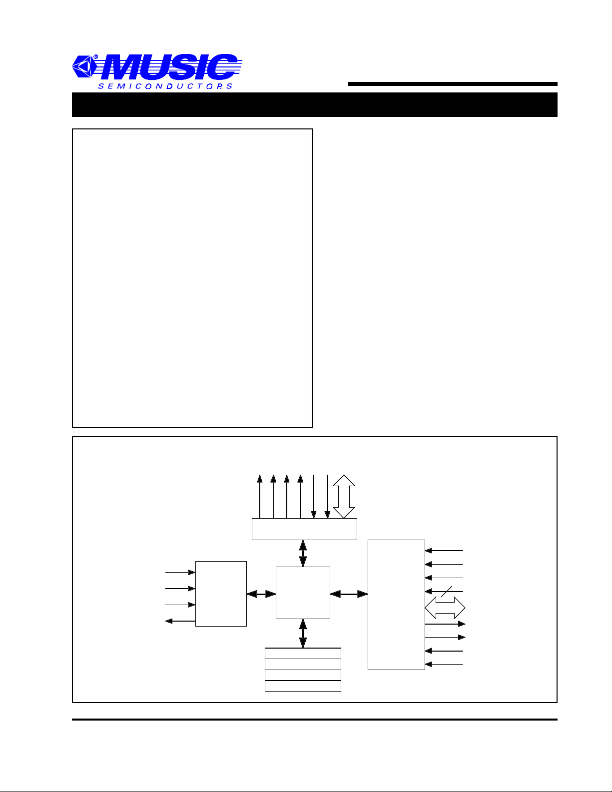
The MU9C8328 speeds up bridging operations using
Ethernet controller chips with serial NRZ data outputs,
such as AMD’s MACE™, National’s SONIC™, and
Motorola’s QUICC™ controllers, by parsing the Ethernet
frame independently of the Ethernet controller device, and
notifying it whether to accept or reject the incoming frame.
The MU9C8328 supports both positive and negative
filtering on the Destination address and learning of new
Source addresses, by efficiently controlling the compare
activities of the MUSIC LANCAM Family. Filtering and
learning routines are user configurable. These routines
are automatically invoked by the internal state machine
based on the contents of the incoming frame and the
configuration settings. For aging and other housekeeping
routines, the MU9C8328 provides the proper sequencing
and timing of LANCAM accesses for an external
processor.
The MU9C8328 receives serial NRZ data from the
Ethernet controller chip, finds the Start delimiter, and
loads the DA and SA into registers. The DA is sent to the
LANCAM for filtering and, depending on the filter action
/E
/CM
/W
/EC
/M F
DQ(15-0)
PROCESSOR
INTERFACE
SERCLK
SERDAT
/N E TRD Y
/REJ ECT
NETW OR K
INTERFACE
/FF
LANC AM IN TER FACE
STATE
MACHINE
CO NT RO L
STAT US
OP-C ODE
ASS OCIATED D ATA
Block Diagram
MUSIC Semiconductors, the MUSIC logo, the phrase “MUSIC Semiconductors”, and LANCAM are registered trademarks of MUSIC
Semiconductors. All other trademarks are registered by their respective owners. MUSIC is a trademark of MUSIC Semiconductors.
/CS
/AS
/W E
3
A(2-0)
D(15-0)
READY
/INT
SYSCLK
/RESET
11 February 1999 Rev. 4a
Page 2

MU9C8328 Ethernet Interface
GENERAL DESCRIPTION
selected, notifies the controller whether to copy or purge
the frame. The SA is then sent to the LANCAM for
comparison, and if no match is found, can be learned
to the Next Free address in the LANCAM. Scheduling
is done within the MU9C8328 so that each filtering
action completes in the time of a minimum length
frame. The filtering and learning routines are
preprogrammed in the MU9C8328, with decision
options set in the control register. A Status register is
provided so the host processor can determine the results
of activities. The specific Op-Code for the LANCAM
Continued
learning instruction is by default a MOV NF , CR, V, but it
can be overridden by writing a value to the Op-Code
register. Aging and purging activity is directly controlled
by the host processor. The READY signal notifies the host
processor that processor operations are complete. The /
INT signal notifies the processor that a network frame
has been processed and the result stored in the Status
register. The processor can turn off the network filtering
activity to have total control of the LANCAM; during this
time the controller can be notified to accept or reject
all frames.
PIN DESCRIPTIONS
All signals are implemented in CMOS technology with TTL levels. Signal names that start with a slash (“/”) are active
LOW. Inputs should never be left floating. Refer to the Electrical Characteristics section for more information.
NETWORK INTERFACE
SERCLK (Serial Clock, Input, TTL)
SERCLK is the nominally 10 MHz clock from the Ethernet
controller chip to the MU9C8328. Frame parsing begins
only after the internal clock detector determines that
SERCLK is valid. Internally pulled down with nominal
50K resistor.
SERDAT (Serial Data, Input, TTL)
SERDAT is the NRZ data from the 10 MHz Ethernet
controller chip. The MU9C8328 uses SERCLK to strobe
SERDAT looking for a Start Frame delimiter (SFD), at
which point it begins filtering and learning activity on
the Destination Address (DA) and Source Address (SA).
/REJECT (Reject, Output, TTL)
The MU9C8328 takes /REJECT LOW to notify the
Ethernet controller chip to reject a frame under conditions
set in the Filter Control register.
/NETRDY (Network Ready, Input, TTL)
If /NETRDY is LOW, the MU9C8328 begins parsing
frame data received on the SERDAT input if SERCLK is
valid. The Ethernet controller chip, or the user, takes
/NETRDY HIGH to indicate that SERCLK or SERDAT
is invalid or is transmitting. The MU9C8328 frame parser
and internal state machines are returned to an idle state
after safely completing any LANCAM activity, while
ignoring any compare results. Internally pulled down with
nominal 50K resistor.
PROCESSOR INTERFACE
SYSCLK (System Clock, Input, TTL)
SYSCLK is a 20 MHz to 33 MHz continuous
clock provided by the host system and is the master clock
within the MU9C8328. It is used to determine the presence
of a valid clock on the SERCLK input, operate the three
internal state machines, and provide the proper timing of
the signals on the LANCAM port. If SYSCLK is below
30 MHz, a LANCAM speed grade of 120 ns is acceptable.
Above 30 MHz, a LANCAM speed grade of 90 ns or better
is required.
/CS (Chip Select, Input, TTL)
/CS is taken LOW by the host processor to gain access to
the registers of the MU9C8328 or to directly access the
LANCAM through the MU9C8328 internal
LANCAM registers. The state of /CS becomes effective
on the rising edge of SYSCLK. When /CS goes HIGH,
the MU9C8328 continues filtering and learning based on
conditions set in the Filter Control register and the frame
activity on the network interface.
/AS (Address Strobe, Input, TTL)
The falling edge of /AS latches the A(2–0) bus, and when
both /AS and /CS are LOW, the processor state machine
is enabled by first rising edge of the SYSCLK to begin
writes into or reads out of the MU9C8328.
Rev . 4a 2
Page 3
MU9C8328 Ethernet Interface
/
PIN DESCRIPTIONS
/WE (Write Enable, Input, TTL)
/WE determines the direction of data flow into or out of
the MU9C8328’s processor interface. It also determines
the state of /W to the LANCAM when the processor is
accessing the MU9C8328’s internal LANCAM registers.
If /WE is LOW , the data is written into the register selected
by the A(2–0) bus. If /WE is HIGH, then data is read
out of the register selected by the A(2–0) bus.
A(2–0) (Address Bus, Input, TTL)
A(2–0) select the internal register in the MU9C8328
accessed by the host processor as shown in Table 1.
A(2–0) are latched by the falling edge of /AS.
D(15–0) (Data Bus, I/O, Three-state TTL)
D(15–0) is the processor data bus into and out of the
MU9C8328, and is demuxed to the internal registers as
selected by the A(2–0) bus. If the register selected is the
Control, Status or Op-Code register, when /WE is LOW,
D(15–0) is loaded on the second rising edge of SYSCLK
after both /AS and /CS are LOW. When /WE is HIGH,
data from the selected register is output to the D(15–0)
Continued
bus on the second rising edge of SYSLCK after both /AS
and /CS are LOW. For CAM access, the write or read
operation is completed when READY returns HIGH. If
/CS is HIGH, or if data is not being read out of the
MU9C8328, the output buffers go to HIGH-Z. Internally
pulled down with nominal 50K resistor.
READY (Ready, Output, Three-state, TTL)
When writing to the Control, Status, or Op-Code register,
READY goes LOW on the first rising edge of SYSCLK
after both /AS and /CS are LOW and returns HIGH on the
next rising edge of SYSCLK. For a read cycle from those
registers, READY may only show a negative-going spike
at the first rising edge of SYSCLK after both /AS and /CS
are LOW. The data will be valid before the next rising
edge of SYSCLK. When writing or reading to/from the
CAM registers, READY will go LOW on the first rising
edge of SYSCLK after both /CS and /AS are LOW.
READY returns HIGH four SYSCLK cycles later,
indicating that the CAM write cycle will complete after
the next rising edge of SYSCLK.
/FF
/M F
/E C
/CM
GND
VCC
RESET
READY
/INT
/W E
/AS
/CS
DQ15
DQ13
DQ12
8
A2
DQ11
73
72
71
9
10
D15
D14
GND
VCC
80
79
77
78
81
82
83
84
85
86
/E
/W
87
88
89
90
91
92
93
94
95
96
97
98
99
100
2
4
3
1
VCC
GND
SYSCLK
A1
DQ14
75
76
74
7
5
6
A0
GND
DQ10
70
69
68
67
DQ7
DQ9
DQ8
VCC
65
66
64
63
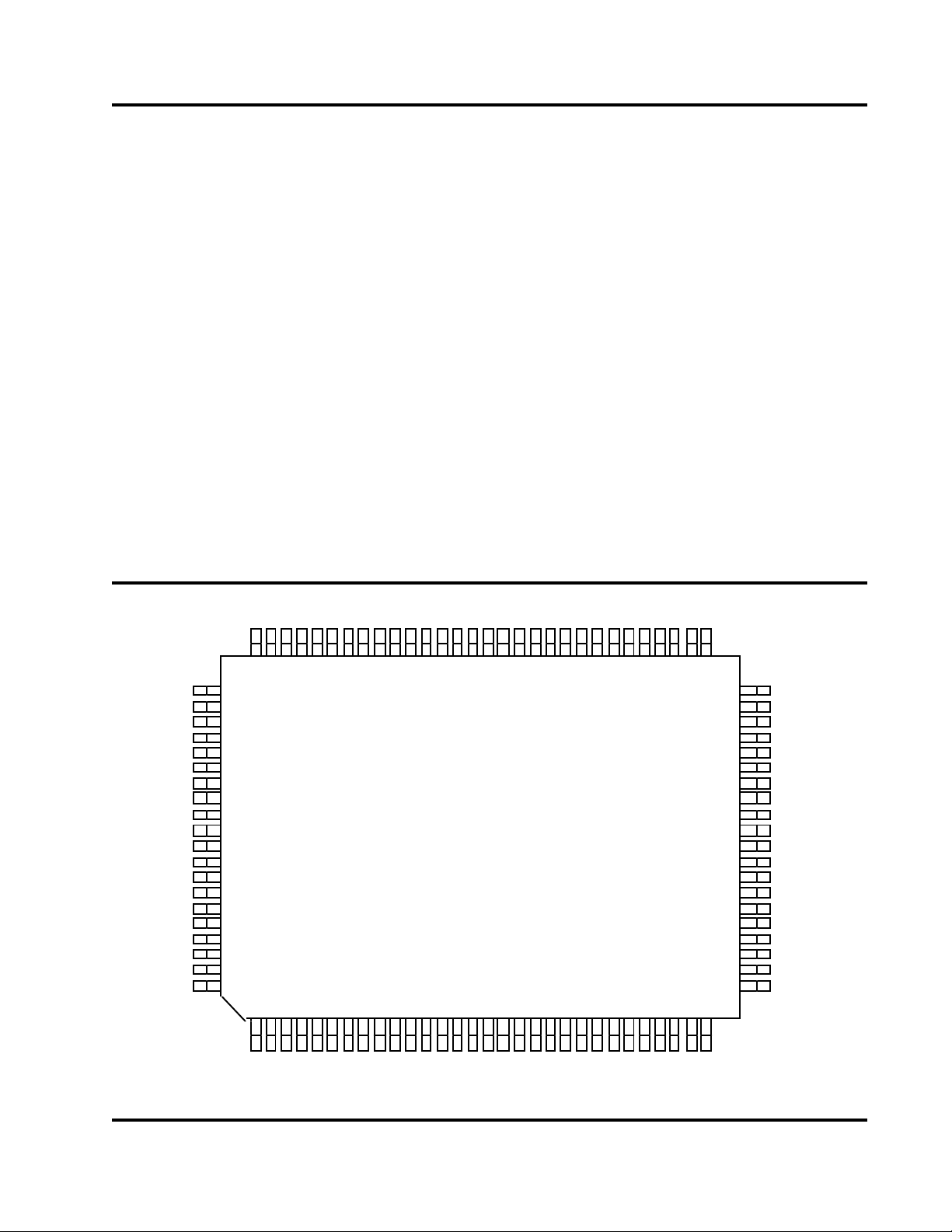
MU9C8328-RDC
100-pin PQFP
(Top View)
17
14
11
12
13
15
16
18
D9
D13
D12
D11
GND
D8
D10
VCC
PINOUT DIAGRAM
DQ6
19
D7
DQ5
DQ4
60
62
61
20
21
D6
D5
59
22
D4
DQ1
DQ2
DQ0
VCC
DQ3
58
57
56
23
24
25
D3
D2
GND
55
54
53
52
51
50
49
48
47
46
45
44
43
42
41
40
39
38
37
36
35
34
33
32
31
27
26
28
29
30
D1
VCC
GND
SERCLK
SE RDAT
/REJECT
NTE ST OUT
NTEST_ E N
GND
VCC
/NE TRDY
D0
3
Rev . 4a
Page 4

MU9C8328 Ethernet Interface
PIN DESCRIPTIONS
/INT (Interrupt, Output, Three-state TTL)
/INT goes LOW to signal the processor that a frame has
been processed, and the results loaded into the Status
register. /INT returns HIGH when the Status register is read.
/RESET (Reset, Input, TTL)
When /RESET is taken LOW, all the internal state
machines are reset to their initial state. Any data stored in
the input address parser is cleared, and the Control, Status,
and Learn Op-Code registers are reset to their default
values. /RESET is synchronous and should be held LOW
for a minimum of two SYSCLK cycles. The user must set
the LANCAM Segment Control register after asserting
/RESET.
LANCAM INTERF ACE
DQ(15–0) (CAM Data Bus, I/O, Three-state TTL)
The DQ(15–0) bus communicates 16-bit data or
instructions between the MU9C8328 and the
LANCAM. When no data is being transmitted by either,
the bus goes HIGH-Z. Internally pulled down with nominal
50K resistor.
Continued
MU9C8328 is outputting data for the LANCAM to place
in its data registers or memory. If /CM is HIGH while /W
is HIGH, the LANCAM is outputting data from one of its
data registers or memory to the MU9C8328.
/EC (Enable Daisy Chain, Output, TTL)
The MU9C8328 takes /EC LOW to control a daisy chain
of LANCAMs by generating the /MF output from the
LANCAM in the case of a match between the contents of
its Comparand register and its memory . When /EC is LOW ,
only the LANCAM containing the match will respond to
write cycles, or output read data. When /EC is HIGH, all
LANCAMs will respond to write cycles.
/MF (Match Flag, Input, TTL)
The LANCAM takes /MF LOW to indicate to the
MU9C8328 that a match was found in its memory with
the contents of its Comparand register. /MF returns HIGH
after the MU9C8328 takes /EC HIGH, or the match
condition is no longer valid. In a daisy chain of
LANCAMs, the /MF signal comes from the /MF output
of the last LANCAM in the string. Internally pulled down
with nominal 50K resistor.
/E (Chip Enable, Output, TTL)
The MU9C8328 takes /E LOW to initiate LANCAM
activity by registering the /W, /CM, /EC, and DQ(15–0)
signals into the LANCAM. /E is taken HIGH to register
returning data into the MU9C8328.
/W (Write Gate, Output, TTL)
The MU9C8328 outputs /W to control the direction of
data flow between the MU9C8328 and the LANCAM. If
/W is LOW at the falling edge of /E, the MU9C8328 is
outputting data to the DQ(15–0) bus for the LANCAM to
input. When /W is HIGH at the falling edge of /E, the
LANCAM outputs data to the DQ(15–0) bus for input to
the MU9C8328.
/CM (Data/Command Select, Output, TTL)
The MU9C8328 outputs /CM to control whether
the LANCAM interprets the DQ(15–0) bus as containing
command information or data. If both /CM and /W are
LOW at the falling edge of /E, the MU9C8328 is outputting
an instruction for the LANCAM to execute, or a value for
one of the LANCAM configuration registers. If /CM is
LOW while /W is HIGH, then the LANCAM will be
outputting data from one of its configuration registers to
the MU9C8328. If /CM is HIGH while /W is LOW, the
/FF (Full Flag, Input, TTL)
The LANCAM takes /FF LOW to indicate to the
MU9C8328 that the LANCAM has no empty locations
remaining. /FF is taken HIGH when the LANCAM has
one or more locations still empty. In a daisy chain of
LANCAMs, the /FF signal comes from the /FF output pin
of the last LANCAM in the string. Internally pulled down
with nominal 50K resistor.
POWER AND GROUND
VCC, GND (Positive Power Supply, Ground)
The VCC pins must be connected externally to a power
source regulated to 5.0 ± 0.25 volts, and should be
adequately bypassed to the Ground pins through
both high and low frequency capacitors. The Ground pins
should all be connected to a common ground plane.
NTTESTOUT
Reserved - Do not connect.
NTEST_EN
Reserved - Tie low.
Rev . 4a 4
Page 5

MU9C8328 Ethernet Interface
FUNCTIONAL DESCRIPTION
The MU9C8328 works with the MUSIC LANCAMs to
provide a complementary and versatile 10 MHz Ethernet
filtering solution for bridges, routers, and switches. Using
the serial NRZ data stream and clock available from many
Ethernet controller chips, the MU9C8328 parses the
incoming frame, finds the Start Delimiter, and forms the
Destination and Source addresses into 16-bit words for
relay to the LANCAM. After all three 16-bit DA segments
have been loaded into the LANCAM, an automatic
compare occurs between the incoming DA and the 48-bit
MAC addresses stored in the LANCAM. If a match is
found, the MU9C8328 is notified, and if Control Register
bit 5 is set for negative filtering, the /REJECT line will be
asserted if Control Register bit 3 is set. An interrupt can
also be generated over the /INT pin if Control Register bit
8 is set. Also, if Control Register bit 0 is set, the Associated
data in segment 0 of the matching entry in the LANCAM
will be retrieved and stored in the Associated Data register
for reading by the host processor. If a match is not found
on the DA, and Control Register bit 5 was set for positive
filtering, the /REJECT line will be asserted. An interrupt
can also be enabled for a no-match on a DA using Control
Register bit 10.
After the DA filtering, the Source Address is loaded
into the LANCAM in three segments. Upon the last
SA load, an automatic compare again takes place. If
there is a match between the SA and an entry in the
CAM, and Control Register bit 7 was set, an interrupt
is asserted. Positive and negative filtering on the SA is
also possible, set by Control Register bit 4, and the /INT
pin may be asserted as well. In the case of a no-match
on an SA, the SA can be automatically “learned” (i.e.,
moved to the first empty location in the LANCAM) if
Control Register bit 1 is set.
If a Loss of Carrier is detected by SERCLK staying LOW
for more than 16 SYSCLK cycles, an interrupt is triggered
if Control Register bit 12 is set. This interrupt also activates
if a collision is detected.
The host processor can access the MU9C8328, shown in
T able 1, at any time, even when a frame is being processed.
Access to the LANCAM through the LANCAM access
registers (04H to 07H) is arbitrated, however, with the
network having precedence. The host processor can have
control of the LANCAM by setting the Network Enable
bit in the Control register (bit 13) to a 0, which will disable
network filtering until it is returned to a 1. While disabled,
bit 14 in the Control register sets the MU9C8328 to accept
all frames by keeping /REJECT HIGH, or to reject all
frames by keeping /REJECT LOW.
Registers 04H through 07H allow the host processor access
to the LANCAM for Command and Data Write and Read
cycles, with /EC HIGH or LOW. This is often needed for
housekeeping activities, such as preventing the LANCAM
from becoming full by aging out old entries based on
timestamps stored in the Associated data (Segment 0) of
the LANCAM memory.
The /INT pin will go LOW at the end of the SA field to
indicate an interrupt for any of the reasons set in the
Control register. Reading the Status register to discover
the nature of the interrupt will take the /INT pin HIGH
again. The READY signal goes LOW after a host processor
write to a register or the LANCAM to indicate that the
Write cycle has begun and return HIGH after a fixed
number of SYSCLK cycles. It will also go LOW during a
read from the LANCAM and return HIGH when the data
from the LANCAM is valid. Since a network compare
activity has precedence over a host process access to the
LANCAM, READY will stay LOW until the network
activity is complete and the host-induced LANCAM read
has completed.
Figure 1 shows a typical network filtering sequence, where
the MU9C8328’s Control register was set to 2109H. This
setting enables network filtering, enables an interrupt for
a match found on the DA, enables negative filtering on
the DA (reject if a DA match is found), enables asserting
the /REJECT pin for compares on the DA, and enables
retrieving the Associated Data field from the matching
location in the LANCAM.
5
Rev . 4a
Page 6

MU9C8328 Ethernet Interface
A(2–0)
0H
0H
1H
1H
2H
2H
3H
3H
4H
4H
5H
5H
6H
6H
7H
7H
/WE
L
H
L
H
L
H
L
H
L
H
L
H
L
H
L
H
FUNCTIONAL DESCRIPTION
Resource Selected
Control Register
Control Register
Reserved
Status Register
Learn Op-Code Register
Learn Op-Code Register
Reserved
Associated Data Register
LANCAM Command Cycle with /EC LOW
LANCAM Command Cycle with /EC LOW
LANCAM Command Cycle with /EC HIGH
LANCAM Command Cycle with /EC HIGH
LANCAM Data Cycle with /EC LOW
LANCAM Data Cycle with /EC LOW
LANCAM Data Cycle with /EC HIGH
LANCAM Data Cycle with /EC HIGH
Table 1: Address Decode
Contined
Action
Write
Read
Read
Write
Read
Read
Write
Read
Write
Read
Write
Read
Write
Read
/CM
/W
/E C
/M F
/REJECT
/INT
DA Match Fou nd SA No-Match/Learn
Pream ble SFD DA 1 SA2 DataLength/TypeSE RDAT DA 2 DA 3 SA1 SA3
/E
Figure 1: Typical Network Filtering
Rev . 4a 6
Page 7

MU9C8328 Ethernet Interface
FUNCTIONAL DESCRIPTION
CONTROL REGISTER (000)
Bit Mnemonic Description
15 DONE 1: Enables an interrupt when both the DA and SA CAM lookup are complete
14 P/R 1: Passes all frames, 0: Rejects all frames (NETEN) must be set to 0 for this option
13 NETEN 1: Enables network filtering, 0: Disables network filtering
12 ERR 1: Enables an interrupt for a frame error caused by loss of carrier or collision
11 FULL 1: Enables an interrupt if the LANCAM is full
10 NODA 1: Enables an interrupt for a no-match on DA
9 NOSA 1: Enables an interrupt for a no-match on SA
8 DA 1: Enables an interrupt for a DA match
7 SA 1: Enables an interrupt for an SA match
6 REJECT 1: Enables an interrupt for a reject
5 DAPON 1: Rejects frame if there is no DA match (positive filtering), 0: Rejects frame if there is
a DA match (negative filtering) (This bit is a “don’t care” if SAEN is 0)
4 SAPON 1: Rejects frame if there is no SA match (positive filtering), 0: Rejects frame if there is
an SA match (negative filtering) (This bit is a “don’t care” if SAEN is 0)
3 DAEN 1: Enables asserting the /REJECT pin after a DA compares, based on bit 5
2 SAEN 1: Enables asserting the /REJECT pin after an SA compares, based on bit 4
1 LEARN 1: Enables auto-learning on no-match of SA
0 ASSOC 1: Enables a read of Associated data after a DA match
STATUS REGISTER (001)
Bit Mnemonic Description
15–8 Reserved
7 COL 1 = Collision detected
6 LOC 1 = Loss of carrier detected
5 BUSY 1 = Network port is busy using the LANCAM
4 MATCH 1 = A match was found
3 FULL 1 = The LANCAM is full
2 DAM 1 = A Destination Address match was found
1 SAM 1 = A Source Address match was found
0 REJECT 1 = The frame was rejected
LEARN OP-CODE REGISTER (010)
Bit Mnemonic Description
15–0 Contains the Op-Code to be used for an auto-learn, if enabled. Default is 0334H (MOV
NF, CR, V), but can be overwritten
Contined
Table 2: Register Descriptions
7
Rev . 4a
Page 8

MU9C8328 Ethernet Interface
APPLICATIONS
Connections
Connection diagrams are shown in Figures 2, 3, and 4 for
National’s SONIC, AMD’s MACE, and Motorola’s
QUICC Ethernet controller chips. Other controller chips
that provide a serial NRZ received data port and clock
can also be used in similar fashions. The /NETRDY line
is provided for controller chips that output data on the
received data line while transmitting. If /NETRDY is
deasserted, the internal network state machine will safely
complete any current activity and then wait until
/NETRDY is asserted again before parsing another frame.
If the controller chip does not output data on the received
data line while transmitting, /NETRDY may be tied to
ground, and the MU9C8328’s valid clock detector will
determine when it is time to start parsing a frame.
LANCAM
/E /EC /MF /FF
/CM /W
DQ(15- 0)
AM79C 940
SRDCLK
SRD
TXEN /NETRDY
/EAM /R
/E /EC /M F /FF/CM /W
SERCLK
SERDAT
/REJECT
MU9C 8328
SYSCLK
/RESET
/CS
/AS
/WE
A(2-0)
D(15-0)
READY
/INT
Initialization of the LANCAM
Before using, the MUSIC LANCAMs need to be configured
for the number of LANCAMs in a daisy chain and for the
filtering conditions in the Control and Segment Control
registers. Before configuring the LANCAMs, bit 13 in the
MU9C8328 Control register needs to be set to 0, to turn off
network filtering. Table 3 shows the steps for configuring
two LANCAMs in a daisy chain. The routine selects register
05H in the MU9C8328, which sends Command Write cycles
to the LANCAM. The sequence shown resets the LANCAMs,
sets the Page address for both LANCAMs in the daisy chain,
then sets the Control and Segment Control registers. If a
Mask register were needed, then the sequence would be
modified to set the Persistent destination to MR1 or MR2,
use MU9C8328 register 06H to write data into the Mask
register, change the final Control register value to 8050H or
8060H instead of 8040H to invoke MR1 or MR2 during
compares, and then resetting the Persistent destination to
LANCAM
/E /EC /M F /FF
/CM /W
DQ(15- 0)
DP83932
RXCo
RXDo
TXE /NETRDY
/PRE J
/E /EC /M F /FF/CM /W
SERCLK
SERDAT
/REJECT
MU9C 8328
SYSCLK
/RESET
/CS
/AS
/WE
A(2-0)
D(15-0)
READY
/INT
Figure 2: AMD’s MACE™ Connection Diagram
/E /EC /M F /FF
/CM /W
/E /EC /M F /FF/CM /W
SERCLK
SERDAT
/NET R D Y
/REJECT
RCLK
RCLK
M C68160
EEST
RX
RXD
M C68360
QUICC
RENA
RENA
/RR J CT
Figure 4: Motorola’s QUICC™ Connection Diagram
Rev . 4a 8
Figure 3: National’s SONIC™ Connection Diagram
LANCAM
DQ(15- 0)
SYSCLK
/RESET
/CS
/AS
MU9C 8328
/WE
A(2-0)
D(15-0)
READY
/INT
Page 9

MU9C8328 Ethernet Interface
APPLICA TIONS
the Comparand register as shown in Table 3. If only one
LANCAM is used, Figure 1 would be modified to replace
steps 8 through 13 with a TCO DS (0228H) followed by
a 0000H.
Enabling Network Activity
After the LANCAMs have been initialized, the MU9C8328
is enabled to begin processing network traffic by setting
bit 13 (NETEN) in its Control register to a 1 along with
the desired filtering actions and interrupt enables.
Step
1
2
3
4
5
6
7
8
9
10
11
12
13
14
15
16
17
18
19
20
21
22
23
24
25
26
27
28
29
30
31
32
33
34
35
36
37
A(2–0)
0H
5H
5H
5H
5H
5H
5H
5H
5H
5H
5H
5H
5H
5H
5H
5H
5H
5H
5H
5H
5H
5H
5H
5H
5H
5H
5H
5H
7H
7H
7H
7H
5H
5H
5H
5H
0H
/WE
L
H
L
L
L
L
L
L
L
L
L
L
L
L
L
L
L
L
L
L
L
L
L
L
L
L
L
L
L
L
L
L
L
L
L
L
L
Mnemonic
TCO_DS
TCO_CT
TCO_PA
SFF
TCO_PA
SFF
TCO_CT
SBR
TCO_CT
TCO_SC
SPD_MR1
SPD_CR
SFR
TCO_CT
SPD_MR1
TCO_SC
SPD_CR
TCO_SC
SPS_HM
D(15–0)
C000H
0000H
0228H
FFFFH
0200H
0000H
0208H
0000H
0700H
0208H
0001H
0700H
0200H
0000H
0619H
0200H
8111H
0210H
0000H
0108H
FFF0H
0100H
0618H
0200H
8041H
0108H
0210H
1C04H
FFF0H
FFFFH
FFFFH
FFFFH
0100H
0210H
3808H
0005H
FC8AH
Comments
Pass all frames during initialization
Command Read to reset LANCAM state machines
Selects all Device Select registers
Selects all LANCAMs
Selects all Control registers
Resets all memory locations
Selects first Page Address register
Writes first Page Address value
Sets Full flag on first LANCAM
Selects second Page Address register
Writes second Page Address value
Sets Full flag on second LANCAM
Selects all Control registers
Resets all Full flags
Select Background Register set
TCO CT
48RAM, 16CAM, MR1, Enhanced mode
Select Segment Control register
Set Read and Write to segment 0
Set Persistent Destination to Mask Register 1
Setup Time Stamp in lowest 4 bits of segment 0
Set Persistent Destination to Comparand register
Select Foreground Register set
Select Command register
48CAM, 16RAM, No Mask, Enhanced mode
Set Persistent Destination to Mask Register 1
Select Segment Control register
Set to write Segments 0, 1, 2, and 3
Write to Segment 0 of MR1
Write to Segment 1 of MR1
Write to Segment 2 of MR1
Write to Segment 3 of MR1
Set Persistent Destination to Comparand register
Select Segment Control register
Write Segments 1–3, Read Segment 0
Set Persistent source to Highest match
Enable filter, Negative filter on DA, enable learn
Table 3: LANCAM Initialization Code
Continued
Responding to Interrupts
Depending on the filtering or error interrupt conditions
set in the MU9C8328 Control Register, the /INT line will
assert at the end of the frame SA field. The host can then
read the MU9C8328 Status register to determine the cause
of the interrupt, whereupon the Status register is reset. If
there was a DA match interrupt and read associated data
was set, then the associated data segment stored in the
LANCAM at the same location that matched the frame’s
DA can be read out of the Associated Data register (03H).
9
Rev . 4a
Page 10

MU9C8328 Ethernet Interface
ABSOLUTE MAXIMUM RATINGS
Supply Voltage
Voltage on all Other Pins
Temperature Under Bias
Storage Temperature
DC Output Current
OPERATING CONDITIONS (voltages referenced to GND at the device pin)
Symbol
V
CC 5.25
V
IH
V
IL
T
A
Symbol
I
CC
V
OH
V
OL
I
IZ
OZ
Parameter Min Typical Units Notes
Operating Supply Voltage
Input Voltage Logic 1
Input Voltage Logic 0
Ambient Operating Temperature
Parameter Min Typical Units Notes
Average Power Supply Current
Output Voltage Logic 1
Output Voltage Logic 0
Input Leakage Current µA
Output Leakage Current µAI
-0.5 Volts to 7.0 Volts
-0.5 to VCC+0.5 Volts (-2.0 Volts for
10 ns, measured at the 50% point)
-40°C to + 85°C
-55°C to +125°C
20 mA (per Output, one at a time,
one second duration)
4.75
5.0
2.0
-0.5
0
ELECTRICAL CHARACTERISTICS
2.4
-2
-10
Stresses exceeding those listed under Absolute
Maximum Ratings may induce failure. Exposure
to absolute maximum ratings for extended periods
may reduce reliability. Functionality at or above
these conditions is not implied.
All voltages are referenced to GND.
Max
Volts
VCC + 0.5
0.8
70
Volts
Volts°C1
Still Air
Max
200
0.4
2
10
mA
Volts
Volts
tELEL=tELEL(min)
I
= -8.0mA
OH
I
= 8.0mA
OL
V
≤ V
≤ V
≤ V
IN
OUT
CC
≤ V
SS
V
SS
DQ
N = HIGH Z
CC;
C
IN
C
OUT
To Device
Under Test
(Includes jig)
CAPACITANCE
Parameter Max NotesSymbol Units
Input Capacitance
Output Capacitance
15
15
AC TEST CONDITIONS
Input Signal Transitions
Input Signal Rise Time
Input Signal Fall Time
Input Timing Reference Level
Output Timing Reference Level
SWITCHING TEST FIGURES
5.0 V olts
C1 = 30 pf
5.0 V olts
R1 = 44 6
R2 = 17 4
Ω
To Device
Under Test
Ω
C1 = 5 pf
R1 = 44 6
R2 = 17 4
pF
pF
0.0 to 3.0 Volts
< 3 ns
< 3 ns
1.5 Volts
1.5 Volts
Ω
Ω
f=1MHz, V
f=1MHz, V
Input
Waveform
0V
50% Amplitude
Point
= 0 V.
IN
OUT
= 0 V.
10ns
IL (MIN)
V
Figure 5: AC Test Load A Figure 6: AC Test Load B
Rev . 4a 10
Figure 7: Input Signal Waveform
Page 11

No
1
2
3
4
5
6
7
8
9
10
11
12
13
14
15
16
17
18
19
20
21
22
23
24
25
26
27
28
29
30
31
32
33
34
35
36
37
38
39
40
41
42
Symbol
tKHKH
tKHKL
tKLKH
tKHCH
tCHKH
tCHCH
tCHCL
tCLCH
tCHNH
tCHNL
tSLKH
tSHKH
tSLSH1
tAVSL
tSLAX
tWLKH
tWL WH
tKHWH
tDVKH
tKHDX
tKHRL
tKHRH
tRLRH1
tTHCH
tCHTL
tYLTV
tKHJL
tKHDZ1
tKHDV
tKHDZ
tRLRH2
tKHEL
tKHEH
tKHGV
tKHGX
tEHML
tRHSH
tSHDZ
tKHDX
tKHDV
tELQV
tEHQZ
SWITCHING CHARACTERISTICS
Parameter (all times in nanoseconds)
SYSCLK Period
SYSCLK HIGH Pulse Width
SYSCLK LOW Pulse Width
SYSCLK HIGH to SERCLK HIGH Set-up Time
SERCLK HIGH to SYSCLK HIGH Set-up Time
SERCLK Period
SERCLK HIGH Pulse Width
SERCLK LOW Pulse Width
SERCLK HIGH to SENSE HIGH
SERCLK HIGH to SENSE LOW Delay Time
Chip or Address Select LOW to SYSCLK HIGH Set-up
Chip or Address Select HIGH to SYSCLK HIGH Set-up
Chip or Address Select LOW Pulse Width - Write Cycle
Address Bus VALID to Address Select LOW Set-up
Address Select LOW to Address Bus INVALID Hold
Write Enable LOW to SYSCLK HIGH Set-up Time
Write Enable LOW Pulse Width
SYSCLK HIGH to Write Enable HIGH Hold Time
Data VALID to SYSCLK HIGH Set-up Time
SYSCLK HIGH to Data INVALID Hold Time
SYSCLK HIGH to Ready LOW Delay Time
SYSCLK HIGH to Ready HIGH Delay Time
Ready LOW Pulse Width-Write Cycle
SERDAT HIGH to SERCLK HIGH Set-up Time
SERCLK HIGH to SERDAT LOW Hold Time
NetReady LOW to SERDAT HIGH Set-up Time
SYSCLK HIGH to REJECT LOW Delay Time
Chip or Address Select LOW Pulse Width-Read Cycle
SYSCLK HIGH to Data VALID Delay Time
SYSCLK HIGH to Data HIGH-Z Delay Time
Ready LOW Pulse Width-CAM Write Cycle
SYSCLK HIGH to CAM Enable LOW Delay Time
SYSCLK HIGH to CAM Enable HIGH Delay Time
SYSCLK HIGH to CAM Controls VALID Delay Time
SYSCLK HIGH to CAM Controls INVALID Delay Time
CAM Enable HIGH to Match Flag LOW Delay Time
Ready HIGH to Chip or Address Select HIGH Set-up
Chip or Address Select HIGH to Data HIGH-Z Delay
SYSCLK HIGH to Data Bus Active-Read
SYSCLK HIGH to Data Bus VALID Delay Time
CAM Enable LOW to DQ Bus VALID-Read
CAM Enable HIGH to DQ Bus HIGH-Z
MU9C8328 Ethernet Interface
Min
30
0.4 · tKHKH
0.4 · tKHKH
0
0
0.4 · tCHCH
0.4 · tCHCH
10
10
2 · tKHKH
10
10
10
tKHKH
10
10
10
10
10
10
2 · tKHKH
5 · tKHKH
5
5
Typ
100
16 · tKHKH
tKHKH
11 · tKHKH
Max
50
0.6 · tKHKH
0.6 · tKHKH
0.6 · tCHCH
0.6 · tCHCH
tCHCH
30
30
30
30
30
30
30
30
30
30
50
85
20
Notes
2
3
4
7
8
5
5
6
6
6
11
Rev . 4a
Page 12

MU9C8328 Ethernet Interface
NOTES
1. -1.0 Volts for a duration of 10 ns measured at the 50% amplitude points for imput-only lines (Figure 7)
2. Plus one SERCLK cycle from the first SERCLK HIGH pulse
3. Before first network data pulse
4. From the SYSCLK that strobed the last DA or SA segment into the LANCAM
5. LANCAM Controls include /W, /CM, and /EC
6. See the LANCAM Handbook for additional information on LANCAM Timing Specs
7. With load specified in Figure 5
8. With load specified in Figure 6
CLOCK TIMING
1
SYSCLK
SERCL K
SENSE
45
7
6
2
8
9
3
10
SYSCLK
/CS
/AS
A(2-0)
/WE
D(15- 0)
READY
PROCESSOR INTERFACE WRITE CYCLE
11
11
14 15
16
21 22
17
19 20
13
13
18
12
12
23
Rev . 4a 12
Page 13

SERCL K
MU9C8328 Ethernet Interface
NETWORK INTERFACE TIMING
SERDAT
/NE T RD Y
SYSCLK
/REJECT
24
10101010110101
26
25
27
PROCESSOR INTERFACE READ CYCLE
SYSCLK
/CS
/AS
A(2-0)
/W E
D(15- 0)
28
28
29
13
30
Rev . 4a
Page 14

MU9C8328 Ethernet Interface
PROCESSOR INTERFACE WRITE CYCLE TO LANCAM
SYSCLK
/CS
/AS
A(2-0)
/W E
D(15- 0)
READY
/CM
/EC
DQ (15- 0)
31
32 33
/E
3534
3534
/W
3534
3534
36
/M F
Rev . 4a 14
Page 15

SYSCLK
/CS
/AS
A(2-0)
MU9C8328 Ethernet Interface
PROCESSOR INTERFACE READ CYCLE FROM LANCAM
37 38
37 38
/W E
D(15- 0)
READY
/E
/CM
/W
/EC
39 40
41 42
DQ (15- 0)
15
Rev . 4a
Page 16

MU9C8328 Ethernet Interface
ORDERING INFORMA TION
P ART NUMBER
MU9C8328 - RDC
PACKAGE
100-PIN PQFP
P ACKAGE OUTLINE
D
D1
TEMPERATURE
0-70° C
A
A2
E1 E
VOLTAGE
5.0 ± 0.25
A1
1
Dim. A Dim. A1 Dim. A2 Dim. b Dim. D Dim. D1 Dim. a Dim. E Dim. E1 Dim. L Dim. L1
100-pin
3.40
0.00
2.80
0.22
PQFP
Max
0.35
±0.25
0.38
MUSIC Semiconductors Agent or Distributor:
USA Headquarters
MUSIC Semiconductors
254 B Mountain Avenue
Hackettstown, New Jersey 07840
USA
Tel: 908/979-1010
http://www.music-ic.com
email: info@music-ic.com
Fax: 908/979-1035
USA Only: 800/933-1550 Tech. Support
888/226-6874 Product Info.
e
23.2
±0.2
b
L1 L
Dimensions are in mm.
20.0
±0.2
MUSIC Semiconductors reserves the right to make changes to
its products and specifications at any time in order to improve
on performance, manufacturability, or reliability. Information
furnished by MUSIC is believed to be accurate, but no
responsibility is assumed by MUSIC Semiconductors for the use
of said information, nor for any infringement of patents or of
other third party rights which may result from said use. No
license is granted by implication or otherwise under any patent
or patent rights of any MUSIC company.
©Copyright 1998, MUSIC Semiconductors
Asian Headquarters
MUSIC Semiconductors
Special Export Processing Zone 1
Carmelray Industrial Park
Canlubang, Calamba, Laguna
Philippines
Tel: +63 49 549 1480
Fax: +63 49 549 1023
Sales Tel/Fax: +632 723 62 15
0.65
Typ.
17.2
±0.2
14.0
±0.2
0.80
±0.15
European Headquarters
MUSIC Semiconductors
Torenstraat 28
6471 JX Eygelshoven
Netherlands
Tel: +31 45 5462177
Fax: +31 45 5463663
1.60
Ref.
Rev . 4a 16
 Loading...