

Page 1
I
®
MUSIC
SEMICONDUCTORS
DATA SHEET DRAFT
DISTINCTIVE CHARACTERISTICS
• Supports High-speed Source Routing or Source Routing
Transparent Bridging for up to eight ports
• Glue-free operation with the MUSIC MU9C1480 LANCAM
and Texas Instruments’ Token Ring chip set
• Configurable for either Motorola or Intel processor
addressing modes
• Complies with the IEEE standards for 4 and 16 Mb/s
Token Ring
• Contains a 128-entry Instruction Buffer that holds up to
seven down-loadable filtering and purging routines,
which can be automatically or directly invoked
GENERAL DESCRIPTION
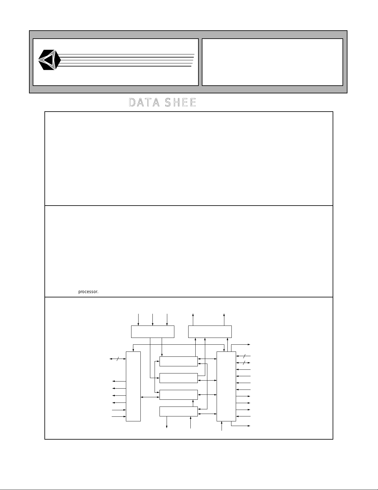
The MU9C8148 is a Source Routing Transparent (SRT) Interface for
the MUSIC Semiconductors MU9C1480 LANCAM for use in Token
Ring LAN Bridges and Brouters. This interface operates in accordance
with IEEE standards while supporting address filtering rates up to
150,000 frames/sec for minimum-length frames.
The MU9C8148 has four interfaces to provide glue-free address
filtering. The Transceiver interface monitors receive data from the
Transceiver to the MAC, and determines whether to filter according to
Source Routing or Transparent Bridging standards. The MAC interface
supplies Match, Fail, and Flush signals to instruct the Token Ring
controller to reject or copy a frame. The LANCAM interface controls the
companion LANCAM(s) for Transparent filtering. The Host Processor
interface allows for direct initialization of the MU9C8148, and
downloading of the filtering and purging routines, to offload the
communication processor.
MU9C8148
SRT Interface
• Automatically selects Source Routed or Transparent
filtering routines based on Transceiver output data, and
supplies the proper Match, Fail, or Flush signals to the
MAC chips
• Built-in arbitration allows two MU9C8148s to share a
central LANCAM database
• Selectable filtering options for each frame type
• Frame validity is checked on all Routing Information
Fields
• Manufactured in CMOS technology
• Available in 68-pin PLCC package and 80-pin TQFP
package
The MU9C8148 can choose to copy or reject a frame depending on the
frame type (MAC, LLC, or reserved), and can perform multiple validity
checks on the Routing Information Field (RIF), including general checks
on every Routing Control Field (RCF), as well as multiple frame related
checks.
The Instruction Buffer can be loaded with up to 128 instructions at
initialization for the LANCAM routines such as matching, learning,
aging, purging, and data buffering operations. Internal arbitration
controls access to the LANCAM. Separate arbitration pins allow two
MU9C8148s to easily form a dual-port Bridge by sharing a central
LANCAM-based station list.
With seven Ring-Bridge-Ring number combinations stored internally,
the MU9C8148 can also operate as a source routing accelerator in
multi-port Token Ring Bridge/Brouter environments.
BLOCK DIAGRAM
/RDY RXD RXC XMATCH XFAIL, /FLUSH
TRANSCEIVER
INTERFACE
/CM
/EC
/MI
16
/E
/W
LANCAM INTERFACE
/FI
DQ15-DQ0
LANCAM, the MUSIC logo, and the phrase “MUSIC Semiconductors” are registered trademarks of MUSIC Semiconductors. MUSIC is a trademark
of MUSIC Semiconductors. This device takes advantage of features in the LANCAM patented under U.S. Patent 5,383,146.
TRANSPARENT
BRIDGING BLOCK
SOURCE ROUTING
BLOCK
INSTRUCTION
BUFFER
ARBITER
/RQ /RQI
MAC
INTERFACE
INTERFACE
HOST PROCESSOR
/INTEL
5
16
/INT
A4-A0
D15-D0
ALE, SRNW
/CS
/RS, /LDS
/WS, /UDS
/HBRDY
/HBEN
/HBDIR
/RESET
/FULL, /EMPTY
15 April 1997 Rev. 5.5 Draft
Web
Page 2
MU9C8148
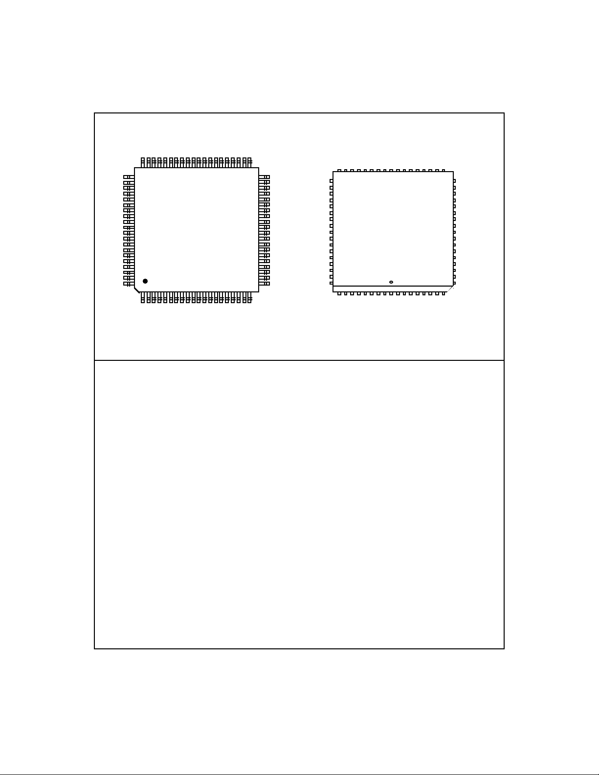
PINOUT DIAGRAMS
NC
NC
D8
DQ5
D9
DQ4
NC
D10
GND
40
D11
39
38
D12
D13
37
D14
36
D15
35
34
/HBRDY
/HBEN
33
/HBDIR
32
/RQ
31
30
/RQI
XFAIL,/FLUSH
29
XMATCH
28
/RDY
27
26
RXD
RXC
25
VCC
24
NC
23
22
NC
GND
21
2019181716151413121110987654321
DQ1
DQ2
DQ0
DQ3
/INT
/FULL,/EMPTY
/INTEL
/RESET
GND
VCC
/WS,/UDS
/CS
VCC
GND
ALE,SRNW
60 59 58 57 56 55 54 53 52 51 50 49 48 47 46 45 44 43 42 41
NC
61
NC
62
63
NC
64
A4
A3
65
A2
66
67
A1
68
A0
69
70
71
72
/EC
73
/CM
74
75
/FI
76
/MI
/E
77
78
/W
79
80
NC
NC
NC
NC
/RS,/LDS
DQ14
DQ15
D2
D1
D0
MU9C8148
80-pin TQFP
DQ11
DQ12
DQ13
D3
DQ10
D4
DQ9
D5
DQ8
D6
DQ7
D7
DQ6
PIN DESCRIPTIONS
(/X indicates an active LOW function)
LANCAM Interface:
DQ15–DQ0 (Data Bus, Input/Output, TTL)
The DQ15–DQ0 lines transfer data, commands and status
between the MU9C8148 and the LANCAM. The direction and
nature of the information that flows between the devices is
determined by the states of /CM and /W.
/E (Chip Enable, Output, Three-state TTL)
The /E output enables the LANCAM while LOW and registers
/W, /CM, /EC and DQ15–DQ0 (if /W is LOW) on the falling
edge of /E. If /W is HIGH, data on DQ15–DQ0 from the
LANCAM is valid on the rising edge of /E.
/W (Write Enable, Output, Three-state TTL)
The /W output selects the direction of data flow during a
LANCAM cycle. DQ15–DQ0 write to the LANCAM if /W is LOW
at the falling edge of /E. Read data is output from the LANCAM
to DQ15–DQ0 on the rising edge of /E if /W is HIGH at the
falling edge of /E.
/CM (Data/Command Select, Output, Three-state
TTL)
The /CM signal determines whether DQ15–DQ0 contain
LANCAM data or commands. /CM is LOW at the falling edge
of /E for Command cycles and HIGH for Data cycles.
XFAIL,/ FLUSH
/HBDIR
/RQ
34
1
2
/RESET
/EC
/RQI
33
3
/CM
32
4
/FI
XMATCH
/RDY
5
6
/E
/MI
RXD
293031
7
/W
RXC
28
8
GND
VCC VCC
27
9
GND
26
DQ0
25
DQ1
24
DQ2
23
DQ3
22
21
DQ4
20
DQ5
19
DQ6
18
DQ7
17
DQ8
16
DQ9
15
DQ10
14
DQ11
13
DQ12
12
DQ13
11
DQ14
10
DQ15
D10
/WS, /UDS
/RS, /LDS
/CS
ALE, SRNW
GND
VCC
/HBRDY
D13
A1
D14
39
65
A0
/HBEN
D15
38
373635
MU9C8148
68-pin PLCC
66
67
68
/INT
/INTEL
/FULL, /EMPTY
GND
D11
D12
424140
43
44
45
D9
46
D8
47
D7
48
D6
49
D5
50
D4
51
D3
52
D2
53
D1
54
D0
55
56
57
58
59
60
626364
61
A3
A4
A2
/EC (Enable Comparison, Output, Three-state TTL)
The /EC signal enables the LANCAM /MF pin to output the
results of a comparison. If /EC is LOW at the falling edge of /E
for a given cycle, the LANCAM /MF output is enabled on the
rising edge of /E. If /EC is HIGH, the LANCAM /MF output is
held HIGH.
/MI (Match Flag, Input, TTL)
The LANCAM /MF pin takes the MU9C8148's /MI input LOW if
a valid match occurs during a Comparison cycle, and /EC was
also LOW at the start of that cycle. The state of the /MI pin
controls branching in the MU9C8148's routines.
/FI (Full Flag, Input, TTL)
The /FI input will be driven LOW by the LANCAM /FF output pin
if all the LANCAM memory locations have valid contents. The
status of the /FI pin can be read by the Host processor from the
MU9C8148's Control register.
Transceiver Interface:
RXD (Receive Data, Input, TTL)
The RXD pin monitors the data received by the TMS38053/4
from the Token Ring. RXD is clocked on the rising edge of
RXC.
Rev. 5.5 Draft
web
2
Page 3

PIN DESCRIPTIONS (CONT’D)
RXC (Receive Clock, Input, TTL)
The rising edge of RXC clocks the RXD data received by the
TMS38053/4 from the Token Ring. The RXC clock is also used
to generate the control signals to the LANCAM, and controls
the internal operation of the MU9C8148.
/RDY (Ring Interface Ready, Input, TTL)
The /RDY pin is taken LOW by the TMS38053/4 to indicate the
presence of received data. /RDY must be HIGH if the RXD data
is not valid.
MAC Interface:
XMATCH (Match, Output, Three-state TTL)
XMATCH goes HIGH in combination with XFAIL going LOW to
indicate that the frame currently being received should be
copied. If XFAIL is HIGH, XMATCH is forced LOW.
XFAIL, /FLUSH (FAIL/FLUSH, Output,
Three-state TTL)
The function of this pin is defined by the Control register. If the
MU9C8148 is connected to a TMS380CX6, this pin is defined
as XFAIL, which goes HIGH when XMATCH goes LOW, to tell
the TMS380CX6 to discard the frame and flush the receive
buffer.
Host Processor Interface:
ALE, SRNW (Address Latch Enable/System Read
Not Write, Input, TTL)
This pin is ALE when the MU9C8148 is used in the Intel mode.
The falling edge of ALE latches the address on the address
lines. If the MU9C8148 is in the Motorola mode, this pin
becomes SRNW, and is HIGH for a Host Processor Read cycle
and LOW for a Write cycle.
/CS (Chip Select, Input, TTL)
/CS going LOW enables the Host Processor interface of the
MU9C8148 for a Host Processor read or write. When /CS is
HIGH, /HBRDY goes three-state and the Host Processor
interface is disabled.
A4–A0 (Address, Input, TTL)
The Address pins select the internal register for Host processor
reads and writes. In the Intel mode, the Address pins are
latched by the falling edge of ALE. In the Motorola mode, the
Address pins must remain stable until the rising edge of /LD
and /UDS, as shown in the Timing diagrams.
MU9C8148
D15–D0 (Data, Common I/O, TTL)
The Data pins transfer data between the Host Processor and
the internal registers of the MU9C8148. The data pins are
registered on the falling edge of /HBRDY in the Write mode,
and are valid on the falling edge of /HBRDY in the Read mode,
as shown in the Timing diagrams.
/RS, /LDS (Read Strobe/Lower Data Strobe,
Input, TTL)
In the Intel mode, this pin is /RS and is taken LOW to begin a
read cycle to the Host Processor interface. Data on D(15-0) is
valid when /HBRDY goes LOW. In the Motorola mode, this pin
is /LDS for Host processor read and write cycles. The falling
edge of /LDS or /UDS begins the cycle; data is strobed when
/HBRDY goes LOW for a Write cycle, and is valid on D(15-0)
when /HBRDY goes LOW for a Read cycle.
/WS, /UDS (Write Strobe/Upper Data Strobe,
Input, TTL)
In the Intel mode, this pin is /WS, and is taken LOW to begin a
write cycle from the Host Processor interface. Data on D(15-0)
is strobed into the MU9C8148 when /HBRDY goes LOW. In the
Motorola mode, this pin is /UDS for Host processor read and
write cycles. The falling edge of /LDS or /UDS begins the Write
cycle; data is strobed when /HBRDY goes LOW for a Write
cycle, and is valid on D(15-0) when /HBRDY goes LOW for a
Read cycle.
/HBRDY (Ready, Output, Three-state TTL)
/HBRDY goes LOW to indicate to the Host processor that a
data transfer is completed for a Write cycle or that data is valid
for a Read cycle. After the Host processor takes /RS, /WS, or
/LDS and /UDS HIGH, the MU9C8148 takes /HBRDY HIGH.
/HBRDY becomes three-state one RXC period after it goes
HIGH, or when /CS goes HIGH.
/HBEN (Data Buffer Enable, Output, TTL)
/HBEN goes LOW to enable external bi-directional buffers, if
are needed on the D15–D0 lines. /HBEN goes HIGH to disable
the external buffers.
/HBDIR (Data Buffer Direction, Output, TTL)
/HBDIR controls the direction of data flow in external
bi-directional buffers. /HBDIR goes LOW to enable data flowing
to the MU9C8148 and HIGH to enable data coming from the
MU9C8148 registers.
/INT (Interrupt, Output, Open Drain)
This pin goes LOW to notify the Host processor that the
MU9C8148 is running an Instruction Buffer routine, therefore
accessing the LANCAM. /INT will remain LOW as long the
routine is running.
3
Rev. 5.5 Draft
web
Page 4
MU9C8148
PIN DESCRIPTIONS (CONT’D)
Arbitration Signals between two MU9C8148s:
/RQ (Request, Output, TTL)
The /RQ pin is used to arbitrate access to a shared LANCAM,
and goes LOW when access is required to the LANCAM. /RQ
of one MU9C8148 is connected to /RQI on the other
MU9C8148 to provide notification that a LANCAM access is
pending. One MU9C8148 is configured as Master, and the
other as Slave, to resolve conflicts. /RQ goes HIGH after the
LANCAM interface transactions are completed.
/RQI (Request Indication, Input, TTL)
If /RQI goes LOW, another MU9C8148 has a request pending
for access to the LANCAM. The LANCAM interface on this chip
is then disabled, and execution of routines is posponed until
/RQI goes HIGH. This pin must be tied HIGH if it is not used.
are 0000H after a Hardware reset (except for register 04H), all
three-state pins are High-Z, and all TTL output pins will be
HIGH.
/FULL, /EMPTY (Full/Empty, Output, Open Drain)
If part of the Instruction buffer in the MU9C8148 is configured
as a FIFO, this active-LOW pin can be configured to signal
whether the FIFO is full (all entries contain valid data) or empty
(no entry contains data). The definition of this signal is
programmed in the FIFO Control register.
/INTEL (HPI Selection, Input, TTL)
The /INTEL pin identifies which type of microcontroller is
connected to the Host Processor interface. This pin is set LOW
for Intel-type addressing modes and HIGH for Motorola-type
addressing modes.
Miscellaneous:
/RESET (Hardware Reset, Input, TTL)
Taking /RESET LOW for at least 2 RXC cycles sets the
MU9C8148 to a predefined state. The contents of all registers
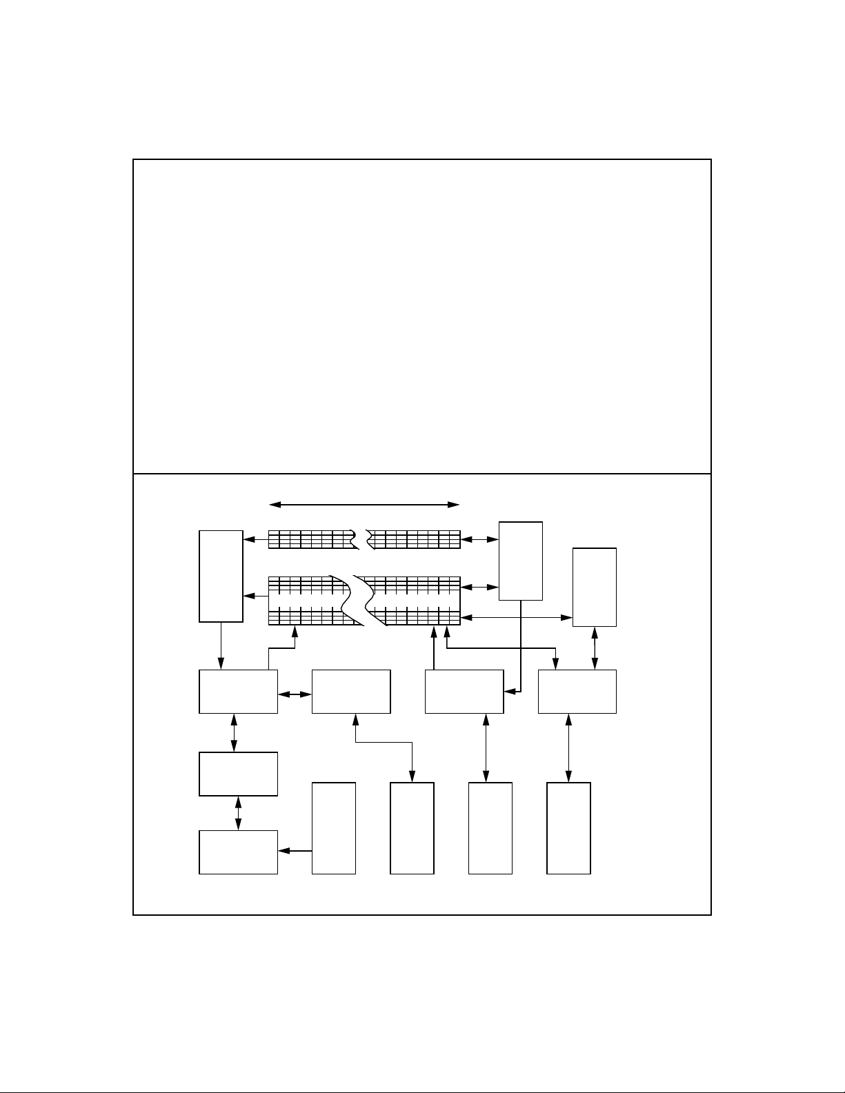
128 Locations
/W, /CM, /EC, S
LANCAM
Interface
Instruction
Pointer and
Control
Arbiter
Start
Address
VCC, GND (Positive Power Supply and Ground)
These pins are the main power supply connections to the
MU9C8148. VCC must be held at +5V ± 10% relative to the
GND pin, which is at 0V (system reference potential), for
correct operation of the device.
IB
D15 - D0
Address
Pointer
Register
FIFO
Control
FIFO
Register
Rev. 5.5 Draft
web
TB block
TB
Register
Start
Address
Register
Control
Register
Figure 1: The Instruction Buffer
4
FIFO
Control
Register
Page 5

FUNCTIONAL DESCRIPTION
Referring to the Block diagram shown on Page 1, the
MU9C8148 consists of four functional blocks: the Transparent
Bridging (TB) block, the Source Routing Block (SRB), the
Instruction Buffer (IB), and the Arbiter. Four interfaces connect
the MU9C8148 to the Transceiver, the MAC controller, the Host
processor, and the LANCAM. For a detailed description of
Token Ring frames, refer to IEEE Standard 802.5, or the IBM
Token-Ring Network Architecture Reference.
Transparent Bridging Block
If a frame does not contain an RIF, the TB block makes
decisions whether to copy or discard a frame based on the
Destination address (DA). If the bridge is set for Transparent
bridging only (the TBO bit in the Control register is HIGH,
disabling the SRB), the TB block also makes copy or discard
decisions for frames which do contain an RIF. The TB block
parses the data as received from the Transceiver off the Token
Ring network, and indicates to the MAC whether to assert the
XMATCH and/or XFAIL (/FLUSH) signals. For each frame, the
TB block examines the Token bit, the Frame Type bits, the
Destination address (DA), and the Source address (SA), which
contains the Routing Information indicator (RII).
The Token bit signals whether the current frame is a Token or a
regular frame. If the Token bit is LOW, a Token frame is being
received, and the TB block discards the frame. For a regular
frame, the Frame Type bits signify the type of frame (LLC,
MAC, or Reserved) being received, and the TB block decides
to copy or discard the frame, based on the settings in the
Frame Type Selection register and the results of filtering on the
Destination address (DA).
Positive or negative filtering on the DA can be done for frames
without an RIF, or for all frames when the bridge is set for
Transparent bridging only, based on the setting of the PONNE
bit in the Transparent Bridging register. Positive filtering implies
that a frame should be forwarded if its DA is found in the
LANCAM address database. Routine 0 in the instruction buffer
examines the DA field to determine whether a frame should be
copied or not. The results of this comparison are used to notify
the LAN controller to copy or discard the frame. Negative
filtering implies that a frame should be forwarded if its DA is not
found in the address database. In this case, the MU9C8148
checks the DA before routine 0 is started to differentiate
between MAC, Broadcast, Functional and Group addresses.
Based upon the settings of the Transparent Bridging register,
the TB block discards a frame whose DA is a Broadcast,
Functional and/or Group address before Routine 0 is started.
If the MU9C8148 is not used in a Transparent Bridging Only
mode and a frame containing an RIF is received, Routine 2 in
the Instruction buffer can be started. The results of this
comparison are combined with the output of the SRB to instruct
the LAN controller to copy or discard the frame. Routine 2 can
only perform positive filtering.
The Source address (SA) of a frame can be used to update the
database of addresses stored in the LANCAM. Routine 1 in the
Instruction buffer checks the SA of a frame against all the
entries in the database, and if the SA is not found, the address
is new, and if the frame received is error free, the address can
be learned by adding it to the LANCAM database. Learning can
MU9C8148
be enabled on the four different frame types (MAC, LLC and
two types of reserved frames) individually. For each frame type,
a choice between two different learning routines can be made
in the Transparent Bridging register. Note that learning can only
take place when the RII bit of the frame is ZERO, or for every
frame when the TBO bit is HIGH. Thus, Routine 0 or Routine 2
is started after the RII bit is received and evaluated. Routine 1
is started by the TB block after the Frame Status field has been
received and the frame found to be error-free.
Source Routing Block
The Source Routing Block (SRB) only decides to copy or
discard a frame if it contains an RIF, and the MU9C8148 is not
in TBO mode. The SRB (in combination with the results of
Routine 2 of the TB) notifies the MAC interface how to assert
its output flags .
When a frame is received, the SRB checks whether the Token
bit in the AC field is LOW, in which case a Token frame is being
received and no further processing is necessary. If the Token
bit is HIGH, a regular frame is being received and the SRB
examines the Frame Type bits in the FC field, which give the
type of frame being received. The frame types to be processed
by the SRB (those with an RIF) are selectable in the Frame
Type Selection register. If the RII bit is HIGH, the SRB signals
the MAC interface, based on the frame type and the settings in
the Frame Type Selection register, either to discard the frame
and flush the buffer, or to continue to check the RIF of the
frame, or to accept the frame. If the RII is LOW, the SRB is not
allowed to process the frame any further and waits for the next
frame to arrive.
If a copy/discard decision is to be made based on the RIF, the
SRB examines the information contained in the RCF. If the
length (LTH) bits of the RCF indicate a length equal to zero, or
contain an odd length, or if the length of the RIF is longer than
the allowed length stored in the RIF Length register, reception
of the frame is stopped, and the SRB indicates that the frame is
to be discarded. The D bit of the Routing Control Field (RCF)
indicates which direction the Routing Descriptors (RDs) of the
RIF should be interpreted.
The SRB provides for seven Ring(in)–Bridge–Ring(out)
combinations (LIN-BN-LOUT) stored in the Source Ring
Number register and Bridge/Destination Ring Number registers.
LIN is the LAN ID of the ring connected to that specific port,
while the BN(s) and LOUT(s) depend on the topology of the
network and the bridge design. The SRB provides for checks
between the LAN ring numbers and bridge numbers contained
in every RD with every LIN-BN-LOUT stored, allowing the user
to develop an SR(T) bridge with an internal virtual ring, or a
bridge with a Full Mesh design (IEEE P802.5M).
If the Routing Type (RT) bits are equal to 0XXB, a
Specifically-Routed Frame (SRF) is being received, and should
be forwarded on the conditions shown in Table 1. If the RT bits
are equal to 10XB, the frame is an All Routes Explorer (ARE)
frame, and should be handled as shown in Table 1. If the RT
bits are equal to 11XB, the frame is a Spanning Tree Explorer
(STE) frame, and should be dealt with as shown in Table 1
Also described in Table 1 are the conditions on which the Error
counters (Register 17H) are incremented.
5
Rev. 5.5 Draft
web
Page 6

MU9C8148
FUNCTIONAL DESCRIPTION (CONT’D)
Condition ActionType
A prestored LIN-BN-LOUT combination is found in the RIF &
that LOUT has occurred only once in the RIF.
A prestored LIN-BN-LOUT combination is found in the RIF &
that LOUT has occurred more than one time in the RIF.
No prestored LIN-BN-LOUT combination is found in the RIF.
Frame
#RDs ≥ SRFRD
Specifically Routed
Prestored LIN is found more than once in the RIF.
LTH = 2
Last LOUT in RIF ≠ LIN, LTH ≠ 2
#RDS ≥ ARERD
Not all prestored LOUTs in RIF
#RDS < ARERD
All Routes Explorer Frame
All prestored LOUTs in RIF, LTH ≠ 2
LTH = 2
Last LOUT in RIF ≠ LIN, LTH ≠ 2
Copy frame. Signal MAC Interface.
Discard frame. Signal MAC Interface.
Increment DUPLOUT counter.
Discard frame. Signal MAC Interface.
Discard frame. Signal MAC Interface.
Discard frame. Signal MAC interface.
Copy frame. Signal MAC Interface.
Discard frame. Signal MAC Interface.
Increment LANIDMISMATCH
counter.
Discard frame. Signal MAC Interface.
Increment ARERDLIMITEXCEEDED
counter.
Copy frame. Signal MAC Interface.
Discard frame. Signal MAC Interface.
.
Copy frame. Signal MAC Interface.
Discard frame, Signal MAC Interface.
Increment LANIDMISMATCH
counter.
#RDS ≥ STERD
Not all prestored LOUTs in RIF
#RDS < STERD
All prestored LOUTs in RIF, LTH ≠ 2
Spanning Tree Explorer Frames
Bit DISSTE = ONE
Note: Signalling takes place at the end of the RIF. Discard actions overrule copy actions. The result of the SRB is
OR’ed with the result of Routine 2, whereby the copy action overrules.
Discard frame. Signal MAC Interface.
Increment STERDLIMITEXCEEDED
counter.
Copy frame. Signal MAC Interface.
Discard frame. Signal MAC Interface.
Increment DUPLANIDORTREEERROR
counter.
Discard frame. Signal MAC Interface.
Table 1: Source Routing Forwarding Conditions
Rev. 5.5 Draft
web
6
Page 7

FUNCTIONAL DESCRIPTION (CONT’D)
Instruction Buffer
The Instruction buffer (IB) shown in Figure 1 consists of the
following: the 128-entry Instruction storage, the Instruction
pointer (IP), the Address pointer, the Start address registers,
the FIFO, and FIFO control registers.
The Instruction Storage (IS) can store up to seven down-loaded
routines which contain instructions for the LANCAM to execute,
plus room for data storage. The IS location accessed by the
Host processor port is controlled by an auto-incrementing
Address pointer, which is part of the Control register. Each
instruction is a 16-bit LANCAM op-code or data word along with
3 bits that indicate the level of /W, /CM, /EC during the
instruction. An additional S-bit is used to indicate whether this
entry is a LANCAM instruction or a MU9C8148 instruction.
The Instruction pointer (IP) points to the instruction currently
executing. At the start of a routine the IP is loaded with the
appropriate Start address. The IP can also be loaded from
Branch Routine addresses or addresses contained in an
instruction itself. For example, when a “Wait for a match”
instruction is executed and no match has occurred, the IP is
loaded with the address of the next instruction to execute.
The Start Address registers contain the start addresses of all
seven routines. When a routine is started, this address is
copied into the IP and execution is started. In addition to the
regular start addresses, two Branch Routine addresses are
available in the IB Start I register and are selected based on
the received frame type, as enabled in the Transparent
Bridging register. If a “Wait for match then execute at Branch
Routine address selected” instruction is executed and no match
occurs, the IP is loaded with the Branch Routine address
selected by the current frame type and execution continues.
Part of the IS may be used as a FIFO for data storage. Data
from the routines can be moved either to or from the Host
Processor interface through the FIFO. While routines are
loaded into the IS from 00H up towards 7FH, the FIFO goes
from 7FH down to the limit set in the FIFO control register. The
functionallity of the /FULL or /EMPTY flag is programmed in the
FIFO Control register to prevent FIFO overflow or underflow
situations.
Programming and Execution of Routines
The IS is loaded and read through the IB register in two 16-bit
cycles. The first 16-bit cycle moves the data on the D15–D0
lines of the Host Processor interface into the data field of the
location in the IB indicated by the Address pointer in the
Control register, or vice-versa in case of a read from the IB
register. The second 16-bit word is written to or read from the
/W, /CM, /EC, and /S bits of that same location.
The Control register contains an Address pointer that selects
the accessed location in the IS. The Address pointer can be
read out or overwritten. It is incremented when the Host
processor has completed the two write or read cycles to one
location of the IB.
Routines in the instruction buffer can be started either by the
Host processor (Routines 3–6 only) or the Transparent Bridging
block. If a routine is started by the Host processor, it can be
MU9C8148
either started directly, or after an RII has been received, or after
the second C bit of the Frame Status field has been received. If
the STDIR bit of a specific routine is set HIGH, the routine is
started immediately. If the START bit of a specific routine is set
to HIGH, the routine is started directly after an RII has been
received (SA/DA is HIGH) or after the second C bit has been
received (SA/DA is LOW). After execution has finished, the
START and STDIR bits are set LOW. If the AUTOSTART bit for
Routines 3, 4, 5 or 6 is set HIGH in the IB Start II register, that
routine is started for every frame received directly after an RII
has been received (when SA/DA is HIGH), or after the second
C bit has been received (when SA/DA is LOW). If more than
one routine should be started at the same time, the routine with
the numerically lowest start address is started first.
The TB block starts Routine 0, 1 or 2 when the enable bit of
that routine is set HIGH. Routines 0 and 2, used for DA
comparison, are started directly after the RII while Routine 1,
used for SA comparison, is started after the last C bit of the FS
field has been received, and if the frame was error-free.
Arbiter
The Arbiter block has two primary tasks: 1) Arbitration between
the execution of different routines stored in the Instruction
Buffer; and, 2) Arbitration between two MU9C8148's when they
are sharing the same LANCAM.
Routine Priorities
Of the seven routines stored in the Instruction buffer, execution
of Routines 0–2 is time critical because there is a direct relation
to the incoming data stream of the Token Ring; therefore, they
have the highest priority and cannot be interrupted by other
routines. The time length of Routines 0 or 2 plus Routine 1
must fit in the time interval of a minimum length frame.
Routines 3–6 have a lower priority and they can be interrupted
by routines having a lower number.
During execution of Routine 0–2, no lower priority routine can
be started. When a second routine is programmed to be started
and execution of the first routine has ended, this second routine
is started immediately afterward. A currently running routine
can be interrupted by a higher priority routine, and the lower
priority routine will re-start from the beginning immediately after
the interrupting routine is finished.
Host Processor Access
The Address bus, A(4-0), is used to select the Registers,
Instruction Buffer, or LANCAM for access from the Host
processor port. Direct access to the LANCAM through registers
18H to 1FH should only be used for LANCAM initialization and
should be completed prior to enabling IB routines. After that,
new addresses written to the LANCAM by the host processor
should be first stored in the IB, and a routine started that
transfers it to the LANCAM. Access to the IB is arbitrated if
network activity triggers a pre-stored routine. The /INT pin goes
LOW (the INT bit in the Control register goes HIGH) to notify
the host processor that a routine is running. (If an access to the
IB is attempted while /INT is LOW, the return of /HBRDY is
delayed slightly until the routine instruction currently executing
is completed.) /INT will stay LOW until all routines have
completed. The processor can then re-issue its request.
Rev. 5.5 Draft
7
web
Page 8

MU9C8148
FUNCTIONAL DESCRIPTION (CONT’D)
For a non-arbitrated Write cycle, /HBEN and /HBDIR go LOW
after the second rising edge of RXC past the falling edge of
/WS (Intel mode) or /UDS and /LDS (Motorola mode). /HBRDY
goes LOW after the second rising edge of RXC past the falling
edge of /HBEN for Register and Instruction Buffer write cycles,
and after the 8th rising edge of RXC past the falling edge of
/HBEN for CAM write cycles. The write data on the D(15-0) bus
is strobed by the rising edge of RXC that outputs /HBRDY.
For a non-arbitrated Read cycle, /HBEN goes LOW after the
third rising edge of RXC past the falling edge of /RS (Intel
mode) or /UDS and /LDS (Motorola mode). /HBRDY goes LOW
after the first rising edge of RXC past the falling edge of /HBEN
for a Register read cycle, the 4th rising edge of RXC past the
falling edge of /HBEN for an Instruction Buffer read cycle, and
the 7th rising edge of RXC past the falling edge of /HBEN for a
CAM read cycle. Read data is output to the D(15-0) bus
immediately prior to /HBRDY going LOW.
For both non-arbitrated Write and Read cycles, /HBRDY goes
HIGH after the first rising edge of RXC past the rising edge of
/WS or /RS in Intel mode or /UDS, /LDS in Motorola mode.
/HBEN and /HBDIR return HIGH and /HBRDY will go
three-state after the next rising edge of RXC.
On a FIFO write, /HBRDY goes LOW after the fifth rising edge
of RXC past the falling edge of /HBEN. On a FIFO read,
/HBRDY goes LOW after the fourth rising edge of RXC past the
falling edge of /HBEN.
MAC Interface
The TB block and/or the SRB notify the MAC interface to copy
or reject a frame through the XMATCH and the XFAIL pins for
the TMS380CX6, or the /FLUSH pin for the 82C581, using the
TEXAS bit in the Control register to select the operating mode.
When Routine 2 is enabled, the results from the TB and the
SRB are combined.
Transceiver Interface
The MU9C8148 connects to the received data bus between the
TMS38053/4 and the TMS380CX6. The differential Manchester
encoded data received from the Token Ring transceiver is input
to the RXD pin which clocked by the RXC clock. The /RDY
signal indicates the presence of received data on the RXD pin.
The Transceiver interface notifies the TB block and the SRB
that it has detected a JK Start delimiter in the incoming data
stream and to begin parsing the other fields of the frame. The
Transceiver interface performs a number of error checks:
whether the data contained any control characters before an
ED was received; that no second SD is received before an ED
is received; and, /RDY is still asserted. In any of these cases,
both the TB and SRB are notified and reception of data is
cancelled. Also checked are: the correctness of the FCS, the
value of the E bit in the ED, and the values of both C bits and
both A bits in the FS field. If there is an error situation detected
in one of these items, the TB is notified not to start Routine 1.
Host Processor Interface
The Host Processor interface is configured for Intel or Motorola
addressing modes using the /INTEL pin. In both modes the
MU9C8148 is a slave on the processor bus and can be
programmed using the registers described in this document.
The MU9C8148 provides /HBEN and /HBDIR to enable the
user to add external bi-directional buffers in the D15-D0
datalines. In Intel mode, ALE is used to latch the address lines.
In Motorola mode, both /UDS and /LDS are used to load the
upper and lower bytes to all of the registers including the
Instruction buffer and FIFO.
Two MU9C8148s Sharing One LANCAM
Two MU9C8148s may share the same LANCAM string if they
are operating at the same frequency, using /RQ and /RQI to
arbitrate the LANCAM access by setting the ASSRQ bit in the
Control register to HIGH. One MU9C8148 is set to be Master,
and given Routines 0–2, and the other is set to be Slave and
given the non-time-critical Routines 3–6 in addition to Routines
0–2. Routines 3–6 running on the Slave can be interrupted
immediately by time-critical routines running on either the
Master or Slave, but if both MU9C8148s try to run a high
priority routine at the same time, the Master device will be
given priority, and the Slave device will start its routine after the
Master has finished.
INSTRUCTION SET DESCRIPTION
Instruction: LANCAM Instruction
Binary Op Code: iiii iiii iiii iiii wce0
i Instruction Code (see The LANCAM Handbook)
w The state of /W
c The state of /CM
e The state of /EC
This instruction transfers data or commands to or from the
LANCAM. Instructions from the LANCAM instruction set are
described in the LANCAM Handbook. The state of the control
outputs /W, /CM and /EC at the falling edge of /E for this cycle
are defined by w,c, and e.
Instruction: Stop Execution
Binary Op Code: 0000 0000 0000 0000 xxx1
x Don't Care
Rev. 5.5 Draft
web
The “Stop Execution” instruction stops the execution of the
routine currently running. Control is transferred to the arbiter.
Instruction: Wait for match for yyyyB + 4 cycles, if no
match then execute at Branch Routine
Address selected.
Binary Op Code: 0001 yyyy rrrr rrrr xxx1
y Wait period
r Reserved (set LOW)
x Don't Care
This instruction waits for a maximum period of yyyyB + 4 clock
cycles for the /MI input to become active, asserting XMATCH
and XFAIL as appropriate. If no match condition occurs during
that period, a branch is executed to the address stored in the
Branch Routine address determined by the frame type. If a
match condition is detected, execution proceeds to the
instruction at the next address.
8
Page 9

INSTRUCTION SET DESCRIPTION (CONT’D)
Instruction: Wait for match for yyyyB + 4 cycles, if no
match then execute at address
aaaaaaaB.
Binary Op Code: 0010 yyyy raaa aaaa xxx1
y Wait period
r Reserved (set LOW)
a Address
x Don't Care
This instruction waits for a maximum period of yyyyB + 4 clock
cycles for the /MI input to become active, asserting XMATCH
and XFAIL as appropriate. If no match condition occurs during
that period, a branch is executed to the address which is stored
in the “a” bits of the instruction. If a match condition is detected,
execution proceeds to the instruction in the next address.
Instruction: Move DA part 0 to DQ15–DQ0.
Binary Op Code: 0011 0000 0000 0000 0ce1
c The state of /CM
e The state of /EC
The “Move DA part 0 to DQ15–DQ0” instruction places the
least significant part of the DA address (bits 15–0) on the
DQ15–DQ0 lines. The control outputs /CM and /EC at the
falling edge of /E for this cycle are defined by c and e.
Instruction: Move DA part 1 to DQ15–DQ0.
Binary Op Code: 0011 0000 0000 0001 0ce1
c The state of /CM
e The state of /EC
The “Move DA part 1 to DQ15–DQ0” instruction places DA
address bits 31–16 on the DQ15–DQ0 lines. The control
outputs /CM and /EC at the falling edge of /E for this cycle are
defined by c and e.
Instruction: Move DA part 2 to DQ15–DQ0.
Binary Op Code: 0011 0000 0000 0010 0ce1
c The state of /CM
e The state of /EC
This instruction places the most significant part of the DA
address (bits 47–32) on the DQ15–DQ0 lines. The control
outputs /CM and /EC at the falling edge of /E for this cycle are
defined by c and e.
Instruction: Move SA part 0 to DQ15–DQ0.
Binary Op Code: 0011 0000 0000 0011 0ce1
c The state of /CM
e The state of /EC
The “Move SA part 0 to DQ15–DQ0” instruction places the
least significant part of the SA address (bits 15–0) on the
DQ15–DQ0 lines. The control outputs /CM and /EC at the
falling edge of /E for this cycle are defined by c and e.
Instruction: Move SA part 1 to DQ15–DQ0.
Binary Op Code: 0011 0000 0000 0100 0ce1
c The state of /CM
e The state of /EC
The “Move SA part 1 to DQ15–DQ0” instruction places SA
address bits 31–16 on the DQ15–DQ0 lines. The control
MU9C8148
outputs /CM and /EC at the falling edge of /E for this cycle are
defined by c and e.
Instruction: Move SA part 2 to DQ15–DQ0.
Binary Op Code: 0011 0000 0000 0101 0ce1
c The state of /CM
e The state of /EC
This instruction places the most significant part of the SA
address (bits 47–32) on the DQ15–DQ0 lines. The control
outputs /CM and /EC at the falling edge of /E for this cycle are
defined by c and e.
Instruction: Move data from address aaaaaaaB to
DQ15–DQ0.
Binary Op Code: 0100 rrrr raaa aaaa 0ce1
r Reserved
a Address
c The state of /CM
e The state of /EC
The “Move data from address aaaaaaaB to DQ15–DQ0”
instruction places the contents of the address specified by the
“a” bits on the DQ15–DQ0 lines. The control outputs /CM and
/EC at the falling edge of /E for this cycle are defined by c and
e.
Instruction: Move data from DQ15–DQ0 to address
aaaaaaaB.
Binary Op Code: 0101 rrrr raaa aaaa 1ce1
r Reserved
a Address
c The state of /CM
e The state of /EC
This instruction places the values on the DQ15–DQ0 lines in
the address specified by the “a” bits. The control outputs /CM
and /EC at the falling edge of /E for this cycle are defined by c
and e.
Instruction: Move data from the FIFO to DQ15–DQ0.
Binary Op Code: 0110 rrrr rrrr rrrr 0ce1
r Reserved
c The state of /CM
e The state of /EC
The “Move data from the FIFO to DQ15–DQ0” instruction
places the contents of the next FIFO location on the
DQ15–DQ0 lines. The control outputs /CM and /EC at the
falling edge of /E for this cycle are defined by c and e.
Instruction: Move data from DQ15–DQ0 to the FIFO.
Binary Op Code: 0111 rrrr rrrr rrrr 1ce1
r Reserved
c The state of /CM
e The state of /EC
This instruction places the values on the DQ15–DQ0 lines into
the FIFO. The control outputs /CM and /EC at the falling edge
of /E for this cycle are defined by c and e.
9
Rev. 5.5 Draft
web
Page 10

MU9C8148
REGISTER SET DESCRIPTION
BIT NAME DESCRIPTION
00H: Control Register
15 RESET If RESET is HIGH, a reset of the MU9C8148 takes place.
14 TEXAS If TEXAS is HIGH, the MU9C8148 is programmed for the Texas Instruments TMS380CX6 MAC con-
13 ASSRQ If ASSRQ is HIGH, the /RQ and /RQI mechanism become active, to permit sharing a LANCAM with
12 M/S If M/S is HIGH, this MU9C8148 is a Master while sharing a LANCAM with another MU9C8148. If this bit
11 TBO If TBO is HIGH, all incoming frames are filtered by the Transparent Bridging block only. No SR bridging
10 DISSTE If DISSTE is HIGH, all Spanning Tree Explorer frames are discarded. The MU9C8148 signals the MAC
9 FF FF indicates the level of the /FI input.
8 RDFCP If RDFCP is HIGH, access to the Error Counter 17H is reset to point to DUPL7–0 and IRI7–0.
7 INT INT indicates the inverse of the level of the /INT output.
6–0 APR6–0 APR6–0 point to the location in the IB which can be accessed through the IB Register.
01H: Frame Type Selection Register
15 MSRENBL If MSRENBL is LOW, every MAC frame containing an RIF is discarded. The MAC is signalled to flush
14 MSRFILT If MSRFILT is LOW, the MU9C8148 signals the MAC chip to copy every MAC frame containing an RIF. If
13 LSRENBL If LSRENBL is LOW, every LLC frame containing an RIF is discarded. The MAC is signalled to flush the
12 LSRFILT If LSRFILT is LOW, the MU9C8148 signals the MAC to copy every LLC frame containing an RIF. If
11 1SRENBL If 1SRENBL is LOW, every reserved type 1 frame containing an RIF is discarded. The MAC is signalled
10 1SRFILT If 1SRFILT is LOW, the MU9C8148 signals the MAC chip to copy every reserved type 1 frame containing
9 2SRENBL If 2SRENBL is LOW, every reserved type 2 frame containing an RIF is discarded. The MAC is signalled
8 2SRFILT If 2SRFILT is LOW, the MU9C8148 signals the MAC to copy every reserved type 2 frame containing an
7 MTRENBL If MTRENBL is LOW, every MAC frame not containing an RIF is discarded. The MAC chip is signalled to
6 MTRFILT If MTRFILT is LOW, the MU9C8148 signals the MAC to copy every MAC frame not containing an RIF. If
5 LTRENBL If LTRENBL is LOW, every LLC frame not containing an RIF is discarded. The MAC chip is signalled to
4 LTRFILT If LTRFILT is LOW, the MU9C8148 signals the MAC to copy every LLC frame not containing an RIF. If
3 1TRENBL If 1TRENBL is LOW, every reserved type 1 frame not containing an RIF is discarded. The MAC is
2 1TRFILT If 1TRFILT is LOW, the MU9C8148 signals the MAC to copy every reserved type 1 frame not containing
troller.
another MU9C8148. If this bit is LOW, both lines are inactive, so no arbitration takes place.
is ZERO, this MU9C8148 is a Slave. If bit ASSRQ is LOW, the M/S bit is “don't care”.
takes place.
to flush these frames. If DISSTE is LOW, STE frames are accepted per the programmed filtering criteria.
the frame. If MSRENBL is HIGH, the MSRFILT bit determines if the frame is filtered or copied directly.
MSRENBL is “don't care” if TBO is HIGH.
MSRFILT is HIGH, the MU9C8148 checks the RIF and forwards the frame if the programmed forwarding
conditions are met. MSRFILT is “don't care” if TBO is HIGH.
frame. If LSRENBL is HIGH, the LSRFILT bit determines if the frame is filtered or copied directly.
LSRENBL is “don't care” if TBO is HIGH.
LSRFILT is HIGH, the MU9C8148 checks the RIF and forwards the frame if the programmed forwarding
conditions are met. LSRFILT is “don't care” if TBO is HIGH.
to flush the frame. If 1SRENBL is HIGH, the 1SRFILT bit determines if the frame is filtered or copied
directly. This bit is “don't care” if TBO is HIGH.
an RIF. If 1SRFILT is HIGH, the MU9C8148 checks the RIF and forwards the frame if the programmed
forwarding conditions are met. This bit is “don't care” if TBO is HIGH.
to flush the frame. If 2SRENBL is HIGH, the 2SRFILT bit determines if the frame is filtered or copied
directly. This bit is “don't care” if TBO is HIGH.
RIF. If 2SRFILT is HIGH, the MU9C8148 checks the RIF and forwards the frame if the programmed
forwarding conditions are met. This bit is “don't care” if TBO is HIGH.
flush the frame. If MTRENBL is HIGH, the MTRFILT bit determines if the frame is filtered or copied
directly. If TBO is HIGH, filtering is also done on MAC frames containing an RIF.
MTRFILT is HIGH, the MU9C8148 checks the DA and forwards the frame if the forwarding conditions
are met, whether or not the frame contains an RIF.
flush the frame. If LTRENBL is HIGH, the LTRFILT bit determines if the frame is filtered or copied
directly. if TBO is HIGH, filtering is also done on LLC frames containing an RIF.
LTRFILT is HIGH, the MU9C8148 checks the DA and forwards the frame if the forwarding conditions are
met, whether or not the frame contains an RIF.
signalled to flush the frame. If 1TRENBL is HIGH, the 1TRFILT bit determines if the frame is filtered or
copied directly. If TBO is HIGH, filtering is also done on reserved type 1 frames with an RIF.
an RIF. If 1TRFILT is HIGH the MU9C8148 checks the DA and forwards the frame if the forwarding
conditions are met, whether or not the frame contains an RIF.
Rev. 5.5 Draft
web
10
Page 11

MU9C8148
REGISTER SET DESCRIPTION (CONT’D)
BIT NAME DESCRIPTION
1 2TRENBL If 2TRENBL is LOW, every reserved type 2 frame not containing an RIF is discarded. The MAC is
0 2TRFILT If 2TRFILT is LOW, the MU9C8148 signals the MAC chip to copy every reserved type 2 frame not
02H: Transparent Bridging Register
15 PONNE If PONNE is LOW, the MU9C8148 performs negative filtering (Routine 0) for frames without an RIF, or
14 DISGA If DISGA is HIGH, all frames with a DA containing a group address and not containing an RIF (or all
13 DISBA If DISBA is HIGH, all frames with a DA containing a broadcast address and not containing an RIF (or all
12 DISFA If DISFA is HIGH, all frames with a DA containing a functional address and not containing an RIF (or all
11 MLRN If MLRN is LOW, no learning of addresses from MAC frames takes place. If this bit is set HIGH, learning
10 LLRN If LLRN is LOW, no learning of addresses from LLC frames takes place. If this bit is set HIGH, learning of
9 1LRN If 1LRN is LOW, no learning of addresses from reserved type 1 frames takes place. If this bit is HIGH,
8 2LRN If 2LRN is LOW, no learning of addresses from reserved type 2 frames takes place. If 2LRN is set HIGH,
7 MROUT If MROUT is LOW, the Branch Routine Address 0 defined in the BR0START6–0 bits in IB Start Register
6 LROUT If LROUT is LOW, the Branch Routine Address 0 defined in the BR0START6–0 bits in IB Start Register I
5 1ROUT When 1ROUT is made LOW, the Branch Routine Address 0 defined in the BR0START6–0 bits in IB
4 2ROUT If 2ROUT is LOW, the Branch Routine Address 0 defined in the BR0START6–0 bits in IB Start Register I
3 0ENBL If 0ENBL is LOW, Routine 0 is disabled. If 0ENBL is HIGH, Routine 0 can be started.
2 1ENBL If 1ENBL is set LOW, Routine 1 is disabled. If 1ENBL is HIGH, Routine 1 can be started.
1 2ENBL If 2ENBL is LOW, Routine 2 is disabled. If 2ENBL is HIGH, Routine 2 can be started.
0 Reserved
03H: RIF Length Register
15 Reserved
14–11 SRFRD3–0 Bits SRFRD3–0 contain the maximum number of RDs–1 for an SRF frame. SRF frames containing more
10 Reserved
9–6 ARERD3–0 Bits ARERD3–0 contain the maximum number of RDs–1 for an ARE frame. ARE frames containing more
5 Reserved
4–1 STERD3–0 Bits STERD3–0 contain the maximum number of RDs–1 an STE frame can contain. If an STE frame
0 Zero Must be set to “0" or LOW.
signalled to flush the frame. If 2TRENBL is HIGH, the 2TRFILT bit determines if the frame is filtered or
copied directly. If TBO is HIGH, filtering is also done on reserved type 2 frames with an RIF.
containing an RIF. If 2TRFILT is HIGH, the MU9C8148 checks the DA and forwards the frame if the
forwarding conditions are met, whether or not the frame contains an RIF.
for all frames when TBO is HIGH. If PONNE is HIGH positive filtering is performed.
frames with a DA containing a group address when TBO = HIGH) are discarded if PONNE is LOW. If
PONNE is HIGH, this bit becomes “don't care”.
frames with a DA containing a broadcast address when TBO = HIGH) are discarded when PONNE is
also programmed LOW. If PONNE is set HIGH, this bit becomes “don't care”.
frames with a DA containing a functional address when TBO = HIGH) are discarded when PONNE is
made LOW. If PONNE is HIGH, this bit becomes “don't care”.
of addresses from MAC frames take place by starting Routine 1 (if starting is enabled), when the frame
doesn't contain an RIF (or for all MAC frames when TBO = HIGH).
addresses from LLC frames take place by starting Routine 1 (if starting is enabled), when the frame
doesn't contain an RIF (or for all LLC frames when TBO = HIGH).
learning of addresses from reserved type 1 frames take place by starting Routine 1 (if starting is
enabled), when the frame doesn't contain an RIF (or for all reserved type1 frames when TBO = HIGH).
learning of addresses from reserved type 2 frames takes place by starting Routine 1 (if starting is
enabled), when the frame doesn't contain an RIF (or for all reserved type 2 frames when TBO = HIGH).
I is selected when a MAC frame is received. If MROUT is HIGH, Branch Routine Address 1 defined in
BR1START6–0 is selected.
is selected when a LLC frame is received. If LROUT is HIGH, Branch Routine Address 1 defined in
BR1START6–0 is selected.
Start Register I is selected when a reserved type 1 frame is received. If 1ROUT is made HIGH, Branch
Routine Address 1 defined in BR1START6–0 is selected.
is selected when a reserved type 2 frame is received. If 2ROUT is HIGH, Branch Routine Address 1
defined in BR1START6–0 is selected.
RDs are not copied by the MU9C8148.
RDs are rejected.
contains more RDs, it is rejected.
11
Rev. 5.5 Draft
web
Page 12

MU9C8148
REGISTER SET DESCRIPTION (CONT’D)
BIT NAME DESCRIPTION
04H: Source Ring Number Register
15–12 ID3–0 ID3–0 contain the version number of the MU9C8148.
11–0 SR11–0 SR11–0 contain the 12-bit Ring Number for this port (Source Ring Number).
05H: Bridge/Destination Ring Number Register A
15–12 BNA3–0 BNA3–0 contain the Bridge Number for remote port A.
11–0 DRA11–0 DRA11–0 contain the Destination Ring Number for remote port A. If DRA11–0 are all LOW,
.
06H: Bridge/Destination Ring Number Register B
15–12 BNB3–0 BNB3–0 contain the Bridge Number for remote port B.
11–0 DRB11–0 DRB11–0 contain the Destination Ring Number for remote port B. If DRB11–0 are all LOW,
07H: Bridge/Destination Ring Number Register C
15–12 BNC3–0 BNC3–0 contain the Bridge Number for remote port C.
11–0 DRC11–0 DRC11–0 contain the Destination Ring Number for remote port C. If DRC11–0 are all LOW,
08H: Bridge/Destination Ring Number Register D
15–12 BND3–0 BND3–0 contain the Bridge Number for remote port D.
11–0 DRE11–0 DRD11–0 contain the Destination Ring Number for remote port D. If DRD11–0 are all LOW,
09H: Bridge/Destination Ring Number Register E
15–12 BNE3–0 BNE3–0 contain the Bridge Number for remote port E.
11–0 DRE11–0 DRE11–0 contain the Destination Ring Number for remote port E. If DRE11–0 are all LOW,
0AH: Bridge/Destination Ring Number Register F
15–12 BNF3–0 BNF3–0 contain the Bridge Number for remote port F.
11–0 DRF11–0 DRF11–0 contain the Destination Ring Number for remote port F. If DRF11–0 are all LOW,
0BH: Bridge/Destination Ring Number Register G
15–12 BNG3–0 BNG3–0 contain the Bridge Number for remote port G.
11–0 DRG11–0 DRG11–0 contain the Destination Ring Number for remote port G. If DRG11–0 are all LOW,
0CH: Instruction Buffer (IB)
First Access
15–0 IB15–IB0 IB15–0 contain the information that is written to or read from the D15–0 bits of the IB location
Second Access
15 /W If LOW, data is written to the LANCAM. If HIGH, data is read from the LANCAM.
14 /CM If LOW, this instruction is a command. If HIGH, this instruction is data.
13 /EC If LOW, the LANCAM will output /MF in the case of a match. If HIGH, /MF is held HIGH.
12 S Special instruction bit. If S is HIGH, the instruction stored at the location pointed to by the address
11–0 Reserved
Bridge/Destination Ring combination A is disabled and doesn't take part in SRB comparisons
Bridge/Destination Ring combination B is disabled and doesn't take part in SRB comparisons.
Bridge/Destination Ring combination C is disabled and doesn't take part in SRB comparisons.
Bridge/Destination Ring combination D is disabled and doesn't take part in SRB comparisons.
Bridge/Destination Ring combination E is disabled and doesn't take part in SRB comparisons.
Bridge/Destination Ring combination F is disabled and doesn't take part in SRB comparisons.
Bridge/Destination Ring combination G is disabled and doesn't take part in SRB comparisons.
(00H to 7FH) pointed to by the address pointer.
pointer is a MU9C8148 instruction. If S is LOW, the instruction is a LANCAM instruction.
Rev. 5.5 Draft
web
12
Page 13

MU9C8148
REGISTER SET DESCRIPTION (CONT’D)
BIT NAME DESCRIPTION
0DH: IB Start Register I
15 Reserved
14–8 BR0START6–0 BR0START6–0 contain the Branch Routine Address 0 of the branch routine that can be started by a
7 Reserved
6–0 BR1START6–0 BR1START6–0 contain the Branch Routine Address 1 of the branch routine that can be started by a
0EH: IB Start Register II
15 AUTOSTART3 AUTOSTART3 is used to make Routine 3 an auto starting routine. If this bit is made HIGH, the routine is
14 STDIR3 If STDIR3 is programmed HIGH, execution of Routine 3 is started directly. After execution has finished
13 START3 If START3 is made HIGH, execution of Routine 3 is started at the point in time indicated by SA/DA3.
12 SA/DA3 If SA/DA3 is made HIGH, execution of Routine 3 takes place directly after the RII has been received. If
11 AUTOSTART4 AUTOSTART4 is used to make Routine 4 an auto starting routine. If AUTOSTART4 is programmed
10 STDIR4 If STDIR4 is made HIGH, execution of Routine 4 is started directly. After execution has finished STDIR4
9 START4 If START4 is HIGH, execution of Routine 4 is started at the point in time indicated by SA/DA4. START4
8 SA/DA4 If SA/DA4 is made HIGH, execution of Routine 4 takes place directly after the RII has been received. If
7 AUTOSTART5 AUTOSTART5 is used to make Routine 5 an auto-starting routine. If AUTOSTART5 is set HIGH, the
6 STDIR5 If STDIR5 is made HIGH, execution of Routine 5 is started directly. After execution has finished STDIR5
5 START5 If START5 is set HIGH, execution of Routine 5 is started at the point in time indicated by SA/DA5.
4 SA/DA5 If SA/DA5 is set HIGH, execution of Routine 5 takes place directly after the RII has been received. If
3 AUTOSTART6 AUTOSTART6 is used to make Routine 6 an auto-starting routine. If AUTOSTART6 is set HIGH, the
2 STDIR6 If STDIR6 is set HIGH, execution of Routine 6 is started directly. After execution is finished, STDIR6 is
1 START6 If START6 is set HIGH, execution of Routine 6 is started at the point in time indicated by SA/DA6.
0 SA/DA6 If SA/DA6 is set HIGH, execution of Routine 6 takes place directly after the RII has been received. If
0FH: Start Address Register I
15 Reserved
14–8 STARTI6–0 STARTI6–0 contain the start address of Routine 1.
7 Reserved
6–0 STARTO6–0 STARTO6–0 contain the start address of Routine 0.
10H: Start Address Register II
15 Reserved
14–8 STARTIII6–0 STARTIII6–0 contain the start address of Routine 3.
7 Reserved
6–0 STARTII6–0 STARTII6–0 contain the start address of Routine 2.
Wait for match then execute at Branch Routine Address selected instruction.
Wait for match then execute at Branch Routine Address selected instruction.
auto starting at the point in time indicated by SA/DA3.
this bit is taken LOW by the MU9C8148.
START3 is taken LOW by the MU9C8148 after execution has been completed.
SA/DA3 is LOW, execution is started after the second C-bit in the FS field.
HIGH, the routine is auto-starting at the point in time indicated by SA/DA4.
is taken LOW by the MU9C8148.
is taken LOW by the MU9C8148 after execution has been completed.
SA/DA4 is LOW, execution is started after the second C-bit in the FS field.
routine is auto starting at the point in time indicated by SA/DA5.
is taken LOW by the MU9C8148.
START5 is taken LOW by the MU9C8148 after execution has been completed.
SA/DA5 is LOW, execution is started after the second C-bit in the FS field.
routine is auto-starting at the point in time indicated by SA/DA6.
taken LOW by the MU9C8148.
START6 is taken LOW by the MU9C8148 after execution has been completed.
SA/DA6 is LOW, execution is started after the second C-bit in the FS field.
13
Rev. 5.5 Draft
web
Page 14

MU9C8148
REGISTER SET DESCRIPTION (CONT’D)
BIT NAME DESCRIPTION
11H: Start Address Register III
15 Reserved
14–8 STARTV6–0 STARTV6–0 contain the start address of Routine 5.
7 Reserved
6–0 STARTIV6–0 STARTIV6–0 contain the start address of Routine 4.
12H: Start Address Register IV
15–7 Reserved
6–0 STARTVI6–0 STARTVI6–0 contain the start address of Routine 6.
13H: FIFO Control Register
15–11 Reserved
10 ENBLFIFO ENBLFIFO enables/disables the FIFO function in the IB. If this ENBLFIFO is HIGH, the FIFO function is
9 RESETFIFO If RESETFIFO is made HIGH, the FIFO read and write pointer are reset to location 7FH. All data stored
8 F/E If F/E is made HIGH the /FULL, /EMPTY output functions like a FIFO full flag. At the moment the FIFO is
7 Reserved
6–0 LIM6–0 LIM6–0 contain the lowest location in the IB the FIFO can use. The FIFO is located between LIM6–0 and
14H: FIFO Register
15–0 FF15–0 FF15–0 contain data that is written in, or read from the FIFO. This data is stored or read from in the
15H: Frame Counter
15–0 FC15–0 The frame counter bits FC15–0 contain the number of frames counted on the Token RIng. It is a 16-bit
16H: Data Counter
First Access
15–0 DC31–16 DC31–16 contain the most significant part of the count of data bytes after the SA received on the
Second Access
15–0 DC15–0 DC15–0 contain the least significant part of the count of data bytes received from the Token RIng.
17H: Error Counter
First Access
15–8 DUPL7–0 DUPL7–0 contain the value of the DUPLOUT counter, which totals the number of frames that were
7–0 IRI7–0 IRI7–0 contain the value of the INVALIDRI counter, which totals the number of frames discarded due to
active. If ENBLFIFO is LOW the FIFO function is inactive and the /FULL, /EMPTY signal is set HIGH.
in the FIFO is lost after a reset.
filled, the /FULL signal is made LOW. If F/E is LOW, the /FULL, /EMPTY output acts like a FIFO empty
flag. It goes LOW when the FIFO is empty.
7FH.
location pointed to by the FIFO pointer. If the /FULL flag indicates that the FIFO is full, the data is lost. If
the /EMPTY flag indicates that the FIFO is empty, no valid data is read.
counter which is increased every time a frame (SD and Token bit set to ONE) is received on the
Transceiver Interface. After overflow, this counter restarts at 0000H.
Transceiver interface. It stops counting after the ED is received, or an SD in an error situation. If there
are other Host Processor cycles between the two consecutive accesses, the result of the second read
out will repeat most significant part of the counter. After overflow, this 32-bit counter starts over at zero.
discarded due to a duplicate LOUT on SRF frames. After readout this error counter is reset to 00H.
various format errors. After readout this error counter is reset to 00H.
Rev. 5.5 Draft
web
14
Page 15

MU9C8148
REGISTER SET DESCRIPTION (CONT’D)
BIT NAME DESCRIPTION
Second Access
15–8 DTE7–0 DTE7–0 contain the value of the DUPLANIDORTREEERROR counter, which totals the number of STE
7–0 LIDM7–0 LIDM7–0 contain the value of the LAN ID MISMATCH counter, which totals the number of ARE and STE
Third Access
15–8 ALIM7–0 ALIM7–0 contain the value of the ARERDLIMIT EXCEEDED counter, which totals the number of ARE
7–0 SLIM7–0 SLIM7–0 contain the value of the STERDLIMIT EXCEEDED counter, which totals the number of STE
18H: LANCAM CWEC Register
15–0 CWEC15–0 Writing to this register starts a direct LANCAM access whereby the data written to CWEC15–0 is placed
19H: LANCAM CREC Register
15–0 CREC15–0 Reading from this register starts a direct LANCAM access whereby the data read from CREC15–0 is
1AH: LANCAM DWEC Register
15–0 DWEC15–0 Writing to this register starts a direct LANCAM access whereby the data written to DWEC15–0 is placed
1BH: LANCAM DREC Register
15–0 DREC15–0 Reading from this register starts a direct LANCAM access whereby the data read from DREC15–0 is
1CH: LANCAM CWNEC Register
15–0 CWEC15–0 Writing to this register starts a direct LANCAM access whereby the data written to CWNEC15–0 is
1DH: LANCAM CRNEC Register
15–0 CRNEC15–0 Reading from this register starts a direct LANCAM access whereby the data read from CRNEC15–0 is
1EH: LANCAM DWNEC Register
15–0 DWNEC15–0 Writing to this register starts a direct LANCAM access whereby the data written to DWNEC15–0 is
1FH: LANCAM DRNEC Register
15–0 DRNEC15–0 Reading from this register starts a direct LANCAM access whereby the data read from DRNEC15–0 is
frames that were discarded because the pre-stored LOUT already exists in the RIF. After readout this
error counter is reset to 00H.
frames that were discarded because the last LAN ID in the RIF did not equal the preset LIN. After
readout this error counter is reset to 00H.
frames discarded due to ARERD Limit exceeded. After readout this error counter is reset to 00H.
frames discarded due to STERD Limit exceeded. After readout this error counter is reset to 00H.
on the DQ15–0 lines and /W, /CM and /EC are held LOW. This register should not be used while
routines are enabled.
data placed on the DQ15–0 lines by the LANCAM. /CM and /EC are held LOW and /W is held HIGH for
this LANCAM cycle. This register should not be used while routines are enabled.
on the DQ15–0 lines and /W and /EC are held LOW while /CM is held HIGH for this LANCAM cycle.
This register should not be used while routines are enabled.
data placed on the DQ15–0 lines by the LANCAM. /EC is held LOW and /W and /CM are held HIGH for
this LANCAM cycle. This register should not be used while routines are enabled.
placed on the DQ15–0 lines and /W and /CM are held LOW while /EC is held HIGH for this LANCAM
cycle. This register should not be used while routines are enabled.
data placed on the DQ15–0 lines by the LANCAM. /CM is held LOW and /W and /EC are held HIGH for
this LANCAM cycle. This register should not be used while routines are enabled.
placed on the DQ15–0 lines and /W is held LOW while /CM and /EC are held HIGH for this LANCAM
cycle. This register should not be used while routines are enabled.
data placed on the DQ15–0 lines by the LANCAM. /EC, /W and /CM are held HIGH for this LANCAM
cycle. This register should not be used while routines are enabled.
15
Rev. 5.5 Draft
web
Page 16

MU9C8148
ABSOLUTE MAXIMUM RATINGS
Supply Voltage -0.5 to 7.0 Volts
Voltage on all Other Pins -0.5 to VCC+0.5 Volts (-2.0 Volts for 10
Temperature Under Bias -40°C to +80°C
Storage Temperature -55°C to +125°C
DC Output Current 20 mA (per Output, one at a time, one
ns, measured at the 50% point)
second duration)
OPERATING CONDITIONS
(voltages referenced to GND at the device pin)
Symbol Parameter Min Typical Max Units Notes
VCC Operating Supply Voltage 4
VIH Input Voltage Logic "1" (HIGH) 2.2 VCC+0.5 Volts
VIL Input Voltage Logic "0" (LOW) -0
TA Ambient Operating Temperature 0 70 °C Still Air
.75 5.05.25 Volts
.50.8 Volts -1.0 Volts for 10 ns measured
ELECTRICAL CHARACTERISTICS
Symbol Parameter Min Typical Max Units Notes
ICC Average Power Supply Current 150 mA
VOH Output Voltage Logic "1" (HIGH) 2
VOL Output Voltage Logic "0" (LOW) 0
IOH Output Open-drain Off Current 5 µA VOH ≤ VCC
IIZ Input Leakage Current -5 5 µA VSS ≤ VIN ≤ VCC
IOZ Output Leakage Current -5 5 µA VSS ≤ VOUT ≤ VCC;
.4 Volts IOH = -2.0 mA (Excl. open-drain outputs)
Stresses exceeding those listed under Absolute
Maximum Ratings may induce failure. Exposure to
absolute maximum ratings for extended periods may
reduce reliability. Functionality at or above these
conditions is not implied.
All voltages are referenced to GND.
.4 Volts IOL = 8.0 mA
DQn = High Impedance
at 50% amplitude, Fig. 5
CAPACITANCE
Symbol Parameter Min Typ Max Units Notes
CIN Input Capacitance 10 pF f=1MHz, VIN=0 Volts
COUT Output Capacitance 10 pF f=1MHz, VOUT=0 Volts
AC TEST CONDITIONS
Input Signal Transitions 0.0 to 3.0 volts
Input Signal Rise and Fall Times ≤3 ns
Input Timing Reference Level 1.5 volts
Output Timing Reference Level 1.5 volts
Open-Drain Reference Level 1.5 volts
TTL Switching Test Load Figure 2
Three-state Test Load Figure 3
Open-Drain Test Load Figure 4
Rev. 5.5 Draft
web
16
Page 17

MU9C8148
SWITCHING CHARACTERISTICS
Arbitration Switching Characteristics
No. Symbol Parameter Min Typ. Max Units Notes
1 tCHRQL /RQ LOW from RXC HIGH 17 ns
2 tCHRQH /RQ HIGH from RXC HIGH 16 ns
3 tRQLCH /RQI to RXC Setup Time 3 ns
MAC Interface Switching Characteristics
No. Symbol Parameter Min Typ. Max Units Notes
4 tCHMFH XMATCH,XFAIL HIGH from RXC HIGH 18 ns
5 tCHMFL XMATCH,XFAIL LOW from RXC HIGH 18 ns
6 tCHFLL /FLUSH LOW from RXC HIGH 18 ns
7 tCHFLH /FLUSH HIGH from RXC HIGH 18 ns
Transceiver Interface Switching Characteristics
No. Symbol Parameter Min Typ. Max Units Notes
8 tRDCH RXD to RXC Setup Time 3 ns
9 tCLCL RXC period 30 31.25 ns 16 Mbit/s TR
125 ns 4 Mbit/s TR
10 tCLCH RXC LOW Period 11 ns
11 tCHCL RXC HIGH Period 11 ns
12 tCHRX RXD from RXC Hold Time 3 ns
SWITCHING TEST FIGURES
5.0 Volts
R1 = 500 ohms
To Device
Under Test
5.0 Volts
C1 = 30 pF
(includes jig)
R2 = 333 ohms
620 ohms
To Device
Under Test
30 pF
Fig. 4: Open-drain Test Load
5.0 Volts
R1 = 500 ohms
To Device
Under Test
R2 = 333 ohms
C1 = 5 pF
Fig. 3: Three-state Test LoadFig. 2: TTL Switching Test Load
INPUT
WAVEFORM
50% AMPLITUDE
POINT
0 V
10 ns
V
IL(MIN)
Fig. 5: Input Signal Waveform
17
Rev. 5.5 Draft
web
Page 18

MU9C8148
SWITCHING CHARACTERISTICS (CONT’D)
Host Processor Interface Switching Characteristics
Intel Mode Timing
No. Symbol Parameter Min Max Units Notes
13 tSHSL /CS HIGH Pulse Width 0 ns
14 tSLKL /CS LOW to ALE LOW Setup Time 2 ns
15 tKHKL ALE HIGH Pulse Width 2 ns
16 tAVKL Address Bus Valid to ALE LOW Setup Time 2 ns
17 tKLAX Address Bus Invalid from ALE LOW Hold Time 5 ns
18 tKLWRL ALE LOW to /WS or /RS LOW Setup Time 0 ns
19 tWLBDL /WS LOW to /HBDIR LOW Delay Time tCLCL + 3 ns
20 tWLBEL /WS LOW to /HBEN LOW Delay Time tCLCL + 3 ns
21 tBDLBEL /HBDIR LOW to /HBEN LOW Delay Time 10 ns
22 tWLDV /WS LOW to Data Input Valid Delay Time 3 •tCLCL ns
23 tWLRDL /WS LOW to /HBRDY LOW Delay Time 3 • tCLCL + 3 ns 1, 2
24 tRDLDX /HBRDY LOW to Data Input Invalid Hold Time tCLCL ns
25 tRDLWRH /HBRDY LOW to /WS or /RS HIGH Setup Time 0 ns
26 tRWHWRL /WS or /RS HIGH Pulse Width 2 • tCLCL ns
27 tWHBDH /WS HIGH to /HBDIR HIGH Delay Time tCLCL + 3 2 • tCLCL + 20 ns
28 tWHBEH /WS HIGH to /HBEN HIGH Delay Time tCLCL + 3 2 • tCLCL + 20 ns
29 tRWHRDH /WS or /RS HIGH to /HBRDY HIGH Delay Time 3 tCLCL + 20 ns
30 tRWHRDZ /WS or /RS HIGH to /HBRDY Hi-Z Delay Time tCLCL + 3 2 • tCLCL + 20 ns
31 tSHRDZ /CS HIGH to /HBRDY Hi-Z Delay Time tCLCL + 3 tCLCL + 20 ns
32 tRLBEL /RS LOW to /HBEN LOW Delay Time 2 • tCLCL + 3 ns 1
33 tRLRDL /RS LOW to /HBRDY LOW Delay Time 3 • tCLCL + 3 ns 1, 3
34 tDVRDL Data Output Valid to /HBRDY LOW Setup Time 2 ns
35 tRHBEH /RS HIGH to /HBEN HIGH Delay Time tCLCL + 3 2 • tCLCL + 20 ns
36 tRHDZ /RS HIGH to Data Output Hi-Z Delay Time tCLCL + 3 2 • tCLCL + 20 ns
Motorola Mode Timing
No. Symbol Parameter Min Max Units Notes
37 tSHSL /CS HIGH Pulse Width 0 ns
38 tSLDSL /CS LOW to /UDS or /LDS LOW Setup Time 0 ns
39 tSRVDSL SRNW Valid to /UDS or /LDS LOW Setup Time 2 ns
40 tAVDSL Address Bus Valid to /UDS or /LDS LOW Setup 2 ns
41 tDSLBDV /UDS or /LDS LOW to /HBDIR LOW Delay Time tCLCL + 3 ns
42 tDSLBEL /UDS or /LDS LOW to /HBEN LOW Delay Time R • tCLCL + 3 ns 1, 4
43 tBDLBEL /HBDIR LOW to HBEN LOW Delay Time 10 ns
44 tDSLDV /UDS or /LDS LOW to Data Input Valid Delay 3 •tCLCL ns
45 tDSLRDL /UDS or /LDS LOW to /HBRDY LOW Delay Time 3 • tCLCL + 3 ns 1, 5
46 tRDLDX /HBRDY LOW to Data Input Invalid Hold Time tCLCL ns
47 tRDLDSH /HBRDY LOW to /UDS or /LDS HIGH Setup Time 0 ns
48 tDSHDSL /UDS or /LDS HIGH Pulse Width 2 • tCLCL ns
49 tDSHSRX /UDS or /LDS HIGH to SRNW Invalid Hold Time 0 ns
50 tDSHAX /UDS or /LDS HIGH to Address Bus Invalid Hold 10 ns
51 tDSHBDX /UDS or /LDS HIGH to /HBDIR Invalid Delay tCLCL + 3 2 • tCLCL + 20 ns
Rev. 5.5 Draft
web
18
Page 19

MU9C8148
Motorola Mode Timing (con't)
No. Symbol Parameter Min Max Units Notes
52 tDSHBEH /UDS or /LDS HIGH to /HBEN HIGH Delay tCLCL + 3 2 • tCLCL + 20 ns
53 tDSHRDH /UDS or /LDS HIGH to /HBRDY HIGH Delay Time 3 tCLCL + 20 ns
54 tDSHRDZ /UDS or /LDS HIGH to /HBRDY Hi-Z Delay Time tCLCL + 3 2 • tCLCL + 20 ns
55 tSHRDZ /CS HIGH to /HBRDY Hi-Z Delay Time tCLCL + 3 tCLCL + 20 ns
56 tDVRDL Data Output Valid to /HBRDY LOW Setup Time 2 ns
57 tDSHDZ /UDS or /LDS HIGH to Data Output Hi-Z Delay tCLCL + 3 2 • tCLCL + 20 ns
LANCAM Interface Switching Characteristics
No. Symbol Parameter Min Typ. Max Units Notes
58 tELEH /E LOW Period 4 • tCLCL ns
59 tEHEL /E HIGH Period R • tCLCL ns 7
60 tCDVEL Control/Data Setup Time to /E LOW 1 ns
61 tELCDX Control/Data Hold Time from /E LOW 120 ns
62 tDVEH Data Setup Time to /E HIGH tCLCL ns
63 tEHDX Data Hold Time to /E HIGH 0 ns
1. If there are routines running due to network activity, access to the device is arbitrated and these times will be
extended by an integer number of RXC cycles, the duration of which will be indicated by /INT going LOW.
2. For non-arbitrated accesses, tWLRDL is 3 RXC cycles for Register writes and for the first write to the
Instruction Buffer, 6 RXC cycles for the second write to the Instruction Buffer or the FIFO, and 9 RXC cyles
for LANCAM writes.
3. For non-arbitrated accesses, tRLRDL is 3 RXC cycles for Register reads, 6 RXC cycles for Instruction Buffer
and FIFO reads, and 9 RXC cycles for LANCAM reads.
4. For non-arbitrated accesses, “R” is 1 for Write cycles and 2 for Read cycles.
5. For non-arbitrated accesses, tDSLRDL is 3 RXC cycles for Register and Instruction Buffer writes, 9 RXC
cycles for LANCAM writes, 3 RXC cycles for Register reads, 6 RXC cycles for Instruction Buffer reads, and 9
RXC cycles for CAM reads.
6. Although the host interface is asynchronous, RXC is used internally to control operations. Therefore, for
modeling purposes, /WS, /RS, /UDS and /LDS can be assumed to have a 10ns setup time with respect to the
rising edge of RXC and /INT, /HBRDY and /FULL can be assumed to assert within 20ns of the rising edge of
RXC. XMATCH and XFAIL assert four RXC cycles after the /MI input is valid.
7. For a data move from DQ15-DQ0 to address, R is 3. For a data move from address to DQ15-DQ0, R is 4.
For a LANCAM register write then read, R is 8. For a LANCAM register write then write, or read then read, R
is 9. For a LANCAM register access read then write, R is 10.
TIMING DIAGRAMS
Notes
RXC
/RQ (SLAVE)
/RQI (SLAVE)
1
2
3
MU9C8148 ARBITRATION TIMING
19
1
Rev. 5.5 Draft
web
Page 20

MU9C8148
TIMING DIAGRAMS (CONT’D)
MAC INTERFACE TIMING
FOR THE TMS380CX6
RXC
XMATCH
XFAIL
54
Rev. 5.5 Draft
web
RXC
RXD
TRANSCEIVER INTERFACE TIMING
9
10
8 12
20
11
Page 21

MU9C8148
TIMING DIAGRAMS (CONT’D)
HOST PROCESSOR INTERFACE TIMING
INTEL-MODE WRITE CYCLE
14
/CS
15
ALE
16
A(4–0)
/WS
/HBDIR
/HBEN
D(15–0) VALID
/HBRDY
17
VALID
18 25
19 27
20 28
22
21
23
24
29
13
26
30
31
/CS
ALE
A(4–0)
/RS
/HBDIR
/HBEN
D(15–0)
/HBRDY
15
16 17
VALID
HOST PROCESSOR INTERFACE TIMING
INTEL-MODE READ CYCLE
18
32 35
34 36
33
25 26
VALID
29
21
1314
30
31
Rev. 5.5 Draft
web
Page 22

MU9C8148
TIMING DIAGRAMS (CONT’D)
HOST PROCESSOR INTERFACE TIMING
38
MOTOROLA-MODE WRITE CYCLE
/CS
/UDS,
/LDS
39
SRNW
40
A(4–0)
41 5143
/HBDIR
42 52
/HBEN
44
D(15–0) VALID
/HBRDY
VALID
45
47
46
53
37
48
49
50
54
55
Rev. 5.5 Draft
web
/CS
/UDS,
/LDS
SRNW
A(4–0)
/HBDIR
/HBEN
D(15–0)
/HBRDY
HOST PROCESSOR INTERFACE TIMING
MOTOROLA-MODE READ CYCLE
47
39
40 50
VALID
42 52
56 57
VALID
45
22
48
49
54
53
3738
55
Page 23

MU9C8148
TIMING DIAGRAMS (CONT’D)
LANCAM WRITE CYCLE TIMING
60
/E
63
62
60 61
/W
58
59
61
/CM
/EC
DQ15-DQ0
/W
VALID
VALID
VALID
LANCAM READ CYCLE TIMING
58 59
60 61
/E
61
62
60
63
/CM
/EC
DQ15-DQ0
VALID
VALID
64
62 63
VALID
65
Rev. 5.5 Draft
web
23
Page 24

MU9C8148
ORDERING INFORMATION
PART NUMBER PACKAGE TEMPERATURE RANGE
MU9C8148-FC 68-PIN PLCC 0-70°C
MU9C8148-TCC 80-PIN TQFP 0-70°C
PACKAGE OUTLINES
He
E
Hd D
80-PIN TQFP
e
b
Lead
Count Dim. A1 Dim. A2 Dim. b Dim. c Dim. D Dim. E
80 0.10 1.40 0.32 0.090 14.00 14.00
±0.05 ±0.05 +0.06 0.200 ±0.10 ±0.10
-0.10
Lead
Count Dim. A Dim. B Dim. C Dim. D Dim. E Dim. E1
.165
68
.200
.013
.021
.020
TYP
A2
A1
L1
L
c
.070
.110
.950
.958
.985
.995
MUSIC Semiconductors
USA Headquarters
MUSIC Semiconductors
254 B Mountain Avenue
Hackettstown, NJ 07840
USA
Tel: (908) 979-1010
Fax: (908) 979-1035
Visit our Web Site at http://www.music.com
MUSIC Semiconductors agent or distributor:
Asian Headquarters
MUSIC Semiconductors
Special Export Processing Zone 1
Carmelray Industrial Park
Canlubang, Calamba, Laguna
The Philippines
Tel: +63 49 549 1480
Fax: +63 49 549 1023/1024
Sales Tel/Fax: +632 723 62 15
Dimensions are in mm.
b
EE1FEE1
a
D
C
F1
A
68-PIN PLCC
a
B
Pin 1
E
E1
F
Dim. e Dim. Hd Dim. He Dim. L Dim. L1
0.65 16.00 16.00 0.60 1.00
±0.10 ±0.10 ±0.15
Dim. F Dim. F1 Dim. a Dim. b
.890
.930
.050
TYP
3°
°
6
®
45
TYP
°
European Headquarters
MUSIC Semiconductors
Torenstraat 28
6471 JX Eygelshoven
The Netherlands
Tel: +31-45-5462177
Fax: +31-45-5463663
MUSIC Semiconductors reserves the right to make changes to its
products and specifications at any time in order to improve on
performance, manufacturability, or reliability. Information furnished
by MUSIC is believed to be accurate, but no responsibility is
assumed by MUSIC Semiconductors for the use of said information,
nor for any infringements of patents or of other third-party rights
which may result from said use. No license is granted by implication
or otherwise under any patent or patent rights of any MUSIC
company.
© Copyright 1997, MUSIC Semiconductors
Rev. 5.5 Draft
web
24
 Loading...