

Datasheet MU9C8480B-70TBC, MU9C8480B-70TBI, MU9C8480B-90TBC, MU9C8480B-90TBI, MU9C1480B-90TAI Datasheet (MUSIC)
...Page 1
Data Sheet
MUSIC Semiconductors, the MUSIC logo, and the phrase "MUSIC Semiconductors" are November 5, 2002 Rev. 2
Registered trademarks of MUSIC Semiconductors. MUSIC is a trademark of
MUSIC Semiconductors.
APPLICATION BENEFITS
• New low-cost LANCAM family in a space-saving
TQFP package
• Fast speed allows processing of both DA and SA
within 450 ns, equival ent to 13 8 ports of 10 Base-T or
13 ports of 100 Base-T Ethernet
• Full CAM features allow all operations to be mas ked
on a bit-by-bit basis
• Powerful, LANCAM A/L compatible instruction set
for any list processing need
• Shiftable Comparand and Mask registers assist in
proximate matching algorithms
• Cascadable to any practical length with no
performance penalties
• Industrial temperature grades for harsh environments
• Dual footprint connections to conserve board space
• 3.3 Volt for lower power systems
DISTINCTIVE CHARACTERISTICS
• High density CMOS Content Addressable Memory
(CAM)
• 1K (1480B), 4K (4480B), 8K (8480B) words
• 64-bit per word memory organization
• 16-bit I/O
• Fast 50 ns compare speed
• Dual configuration register set for rapid context
switching
• 16-bit CAM/RAM segments with MUSIC’s patented
partitioning
• /MA and /MM output flags to enable faster system
performance
• Readable Device ID
• Selectable faster operating mode with no wait states
after a no-match
• Validity bit setting accessible from the Status register
• Single cycle reset for Segment Control register
• 44- and 64-pin TQFP package
• 3.3 Volt operation
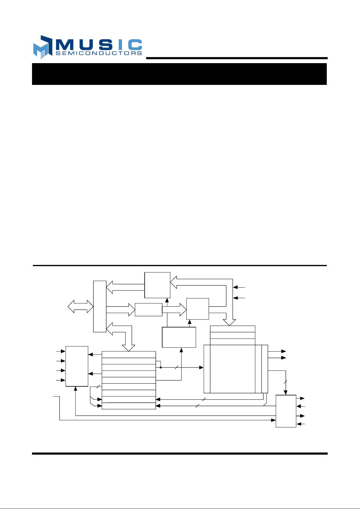
Figure 1: LANCAM B Family Block Diagram
/EC
DQ(15—0) (16)
CAM ARRAY
2
N
WORDS
X 64 BITS
COMPARAND*
MASK 1
MASK 2
2
N
X
2
V
A
L
I
D
I
T
Y
B
I
T
S
P
R
I
O
R
I
T
Y
E
N
C
O
D
E
R
COMMANDS & STATUS
2
N
DATA (16)
TRANSLATE
802.3/802.5
DATA (16)
DEMUX
NEXT FREE ADDRESS (R/O)
CONTROL
SEGMENT CONTROL
PAGE ADDRESS (LOCAL)
DEVICE SELECT (GLOBAL)
ADDRESS
STATUS (31-16) (R/O)
REGISTER SET
2
MATCH ADDR
& /MA FLAG
/MM, /FL
DATA (16)
(16)
DATA (64)
DATA (64)
A
D
D
R
E
S
S
D
E
C
O
D
E
R
/MA
/MM
N+1
16
I
/
O
B
U
F
F
E
R
S
CONTROL
SOURCE AND
DESTINATION
SEGMENT
COUNTERS
MUX
VCC
GND
/FF
/FI
/MF
/MI
MATCH
AND
FLAG
LOGIC
/W
/E
/CM
/RESET
INSTRUCTION(W/O)*
STATUS (15-0) (R/O)*
LANCAM B F amily
LANCAM B F amilyLANCAM B F amily
LANCAM B F amily
Page 2

LANCAM B Family General Description
2
Rev. 2
GENERAL DESCRIPTION
The LANCAM consists of various depths of 64-bit
Content Addressable Memories (CAMs), with a 16-bit
wide interface.
CAMs, also known as associative memories, operate in the
converse way to random access memories (RAM). In
RAM, the input to the device is an address and the output
is the data stored at that address. In CAM, the input is a
data sample and the output is a flag to indicate a match and
the address of the matching data. As a result, CAM
searches large databases for matching data in a short,
constant time period, no matter how many entries are in
the database. The ability to search data words up to 64 bits
wide allows large address spaces to be searched rapidly
and efficiently. A patented architecture links each CAM
entry to associated data and makes this data available for
use after a successful compare operation.
The MUSIC LANCAMs are ideal for address filtering and
translation applications in LAN switches and routers. The
LANCAMs are also well suited to encryption, database
accelerators, and image processing.
OPERATIONAL OVERVIEW
To use the LANCAM, the user loads the data into the
Comparand register, which is automatically compared to
all valid CAM locations. The device then indicates
whether or not one or more of the valid CAM locations
contains data that matches the target data. The status of
each CAM location is determined by two validity bits at
each memory location. The two bits are encoded to render
four validity conditions: Valid, Empty, Skip, and RAM,
shown in Status Register Bits on page 24 (bits 29:28). The
memory can be partitioned into CAM and associated
RAM segments on 16-bit boundaries, but by using one of
the two available Mask registers, the CAM/RAM
partitioning can be set at any arbitrary size between zero
and 64 bits.
The LANCAM’s internal data path is 64 bits wide for
rapid internal comparison and data movement. Vertical
cascading of additional LANCAMs in a daisy chain
fashion extends the CAM memory depth for large
databases. Cascading requires no external logic. Loading
data to the Control, Comparand, and Mask registers
automatically triggers a compare. Compares also may be
initiated by a command to the device. Associated RAM
data is available immediately after a successful compare
operation. The Status register reports the results of
compares including all flags and addresses. Two Mask
registers are available and can be used in two different
ways: to mask comparisons or to mask data writes. The
RAM validity type allows additional masks to be stored in
the CAM array where they may be retrieved rapidly.
A simple four-wire control interface and commands
loaded into the Instruction decoder control the device. A
powerful instruction set increases the control flexibility
and minimizes software overh ead. Additionally, dedicated
pins for match and multiple-match flags enhance
performance when the device is controlled by a state
machine. These and other features make the LANCAM a
powerful associative memory that drastically reduces
search delays.
Page 3

Pin Descriptions LANCAM B Family
Rev. 2 3
PIN DESCRIPTIONS
Note: All signals are implem ented in CMOS technology with TTL levels. Signal names that start with a slash (“/”) are active LOW.
Inputs should never be left flo ating. The CAM architecture draws large currents durin g comp are operations, mandating the use of good
layout and bypassing techniques. Refer to the DC Electrical Characteristics on page 25 for more information.
Figure 2: 44-Pin TQFP Figure 3: 64-Pin TQFP
/E (Chip Enable, Input, TTL)
The /E input enables the device while LOW. The falling
edge registers the control signals /W, /CM, and /EC. The
rising edge locks the daisy chain, turns off the DQ pins,
and clocks the Destination and Source Segment counters.
The four cycle types enabled by /E are shown in Table 1.
/W (Write Enable, Input, TTL)
The /W input selects the direction of data flow during a
device cycle. /W LOW selects a Write cycle and /W HIGH
selects a Read cycle.
/CM (Data/Command Select, Input, TTL)
The /CM input selects whether the input signals on
DQ15–0 are data or commands. /CM LOW selects
Command cycles and /CM HIGH selects Data cycles.
/EC (Enable Daisy Chain, Input, TTL)
The /EC signal performs two functions. The /EC input
enables the /MF output to show the results of a
comparison, as shown in Figure 9 on page 14. If /EC is
LOW at the falling edge of /E in a given cycle, the /MF
output is enabled. Otherwise, the /MF output is held
HIGH.
The /EC signal also enables the /MF–/MI daisy chain,
which serves to select the device with the highest-priority
match in a string of LANCAMs. Table 4 explains the
effect of the /EC signal on a device with or without a
match in both Standard and Enhanced modes. /EC must be
HIGH during initialization.
DQ15–0 (Data Bus, I/O, TTL)
The DQ15–0 lines convey data, commands, and status to
and from the LANCAM. /W and /CM cont rol th e dir ection
and nature of the information that flows to or from the
device. When /E is HIGH, DQ15–0 go to HIGH-Z.
/MF (Match Flag, Output, TTL)
The /MF output goes LOW when one or more valid
matches occur during a compare cycle. /MF becomes valid
after /E goes HIGH on the cycle that enables the daisy
chain (on the first cycle that /EC is registered LOW by the
previous falling edge of /E; see Figure 9 on page 14). In a
daisy chain, valid match(es) in higher priority devices are
passed from the /MI input to /MF. If the daisy chain is
enabled but the match flag is disabled in the Control
register, t he /MF output only depends on the /MI input of
the device (/MF=/MI). /MF is HIGH if there is no match
or when the daisy chain is disabled (/E goes HIGH when
/EC was HIGH on the previous falling edge of /E). The
System Match flag is the /MF pin of the last device in the
daisy chain. /MF is reset when the active configuration
register set is changed.
44-Pin TQFP
(Top View)
/MM
/FF
/FI
/CM
/EC
GND
DQ0
DQ1
DQ2
DQ3
VCC
GND
DQ4
DQ5
VCC
VCC
TEST2
GND
GND
DQ6
DQ7
VCC
GND
DQ15
DQ14
DQ13
DQ12
GND
DQ11
DQ10
DQ9
DQ8
GND
/MA
/MI
/MF
GND
/
RESE
VCC
VCC
TEST1
/E
/W
GND
22
21
20
19
18
17
16
15
14
13
12
33
32
31
30
29
28
27
26
25
24
23
1
2
3
4
5
6
7
8
9
10
11
34
35
36
37
38
39
40
41
42
43
44
DQ15
DQ14
DQ13
DQ12
16
15
14
13
12
1
2
3
4
5
6
7
8
9
10
11
22
21
20
19
18
17
24
23
28
27
26
25
32
31
30
29
37
38
39
40
41
42
43
44
33
34
35
36
45
46
47
48
585960616263 5657 52535455 495064 51
NC
DQ4
DQ5
VCC
VCC
TEST2
GND
GND
DQ6
DQ7
VCC
NC
GND
GND
GND
NC
GND
GND
DQ11
DQ10
DQ9
DQ8
GNDNCGND
GND
GND
NC
/MA
/MI
/MF
GND
/RESET
VCC
VCC
TEST1
/E
/W
GND
NC
NC
GND
GND
NC
64-Pin TQFP
(Top View)
/MM
/FF
/FI
/CM
/EC
GND
DQ0
DQ1
DQ2
DQ3
VCC
NC
NC
GND
NC
NC
Table 1: I/O Cycles
/W /CM Cycle Type
LOW LOW Command Write Cycle
LOW HIGH Data Write Cycle
HIGH LOW Command Read Cycle
HIGH HIGH Data Read Cycle
Page 4

LANCAM B Family Pin Descriptions
4
Rev. 2
/MI (Match Input, Input, TTL)
The /MI input prioritizes devices in vertically cascaded
systems. It is connected to the /MF output of the previous
device in the daisy chain. The /MI pin on the first device in
the chain must be tied HIGH.
/MA (Device Match Flag, Output, TTL)
The /MA output is LOW when one or more valid matches
occur during the current or the last previous compare
cycle. The /MA output is not qualified by /EC or /MI, and
reflects the match flag from that specific device’s Status
register. /MA is reset when the active register set is
changed.
/MM (Device Multiple Match Flag, Output, TTL)
The /MM output is LOW when more than one valid match
occurs during the current or the last previous compare
cycle. The /MM output is not qualified by /EC or /MI, and
reflects the multiple match flag from that specific device’s
Status register. /MM is reset when the active register set is
changed.
/FF (Full Flag, Output, TTL)
If enabled in the Control register, the /FF output goes
LOW when no empty memo ry locations exist within the
device (and in the daisy chain above the device as
indicated by the /FI pin). The System Full flag is the /FF
pin of the last device in the daisy chain, and the Next Free
address resides in the device with /FI LOW and /FF
HIGH. If disabled in th e Control register, the /FF output
only depends on the /F I input (/FF = /FI).
/FI (Full Input, Input, TTL)
The /FI input generates a CAM-Memory-System-Full
indication in vertically cascaded systems. It is connected
to the /FF output of the previous device in the daisy chain.
The /FI pin on the first device in a chain must be tied
LOW.
/RESET (Reset, Input, TTL)
/RESET must be driven LOW to place the device in a
known state before operation, which resets the device to
the conditions shown in Table 3 on page 11. The /RESET
pin should be driven by TTL levels, not directly by an RC
timeout. /E must be kept HIGH during /RESET.
TEST1, TEST2 (Test, Input, TTL)
These pins enable MUSIC production test modes that are
not usable in an application. They should be connected to
ground, either directly or through a pull-down resistor, or
they may be left unconnected. These pins may not be
implemented on all versions of these products.
VCC, GND (Positive Power Supply, Ground)
These pins are the power supply connections to the
LANCAM. VCC must meet the voltage supply
requirements in the Operating Conditions section relativ e
to the GND pins, which are at 0 volts (system reference
potential), for correct operation of the device. All the
ground and power pins must be connected to their
respective planes with adequate bulk and high frequency
bypassing capacitors in close proximity to the device.
Page 5

Functional Description LANCAM B Family
Rev. 2 5
FUNCTIONAL DESCRIPTION
The LANCAM is a Content Addressable Memory (CAM)
with 16-bit I/O for network address filtering and
translation, virtual memory, data compression, caching,
and table lookup applications. The memory consists of
static CAM, organized in 64-bit data fields. Each data field
can be partitioned into a CAM and a RAM subfield on
16-bit boundaries. The contents of the memory can be
randomly accessed or associatively accessed by the use of
a compare. During automatic comparison cycles, data in
the Comparand register is automatically compared with
the “Valid” entries in the memory array. The Device ID
can be read using a TCO PS instruction (see Persistent
Source Register Bits on page 24).
Data Input and Output Characteristics
The data inputs and outputs of the LANCAM are
multiplexed for data and instructions over a 16-bit I/O bus.
Internally, data is handled on a 64-bit basis, since the
Comparand register, the Mask registers, and each memory
entry are 64 bits wide. Memory entries are globally
configurable into CAM and RAM segments on 16-bit
boundaries, as described in US Patent 5,383,146 assigned
to MUSIC Semiconductors. Seven different CAM/RAM
splits are possible, with the CAM width going from one to
four segments, and the remaining RAM width going from
three to zero segments. Finer resolution on compare width
is possible by invoking a Mask register during a compare,
which allows global masking on a bit basis. The CAM
subfield contains the associative data, which enters into
compares, while the RAM subfield contains the associated
data, which is not compared. In LAN bridges, the RAM
subfield co uld hold, for exam ple, port-address a nd aging
information related to the destination or source address
information held in the CAM subfield of a given location.
In a translation application, the CAM field could hold the
dictionary entries, while the RAM field holds the
translations, with almost instantaneous response.
Validity Bits
Each entry has two validity bits associated with it to define
its particular type: Empty, Valid, Skip, or RAM. When
data is written to the active Comparand register, and the
active Segment Control register reaches its terminal count,
the contents of the Comparand register are automatically
compared with the CAM portion of all the vali d entries in
the memory array. For added versatility, the Comparand
register can be barrel-shifted right or left one bit at a time.
A Compare instruction then can be used to force another
compare between the Comparand register and the CAM
portion of memory entries of any one of the four validity
types. After a Read or Move from Memory operation, the
validity bits of the location read or moved are copied into
the Status register, where they can be read using
Command Read cycles.
Data Movement (Read/Write)
Data can be moved from one of the data registers (CR,
MR1, or MR2) to a memory location that i s based on the
results of the last comparison (Highest-Priority Match or
Next Free), or to an absolute address, or to the location
pointed to by the active Address regist er. Data can also be
written directly to the memory from the DQ bus using any
of the above addressing modes . The Address register may
be directly loaded and may be set to increment or
decrement, allowing DMA-type reading or writing from
memory.
Configuration Register Sets
Two sets of configuration registers (Control, Segment
Control, Addre ss, Mask Reg ister 1, and Persi stent Sourc e
and Destination) are provided to permit rapid context
switching between foreground and background activities.
The currently active set of configuration registers controls
writes, reads, moves, and compares. The foreground set
typically would be pre-loaded with values useful for
comparing input data, often called filtering, while the
background set would b e pre- loaded with values useful for
housekeeping activities such as purging old entries.
Moving from the foreground task of filtering to the
background task of purging can be done by issuing a
single instruction to change the current set of
configuration registers. The match condition of the device
is reset whenever the active register set is changed.
Control Register
The active Control register determines the operating
conditions within the device. Conditions set by this
register’s contents are reset, enable or disable Match flag,
enable or disable Full flag, CAM/RAM partitioning,
disable or select masking conditions, disable or select
auto-incrementing or auto-decrementing the Address
register, and select Standard or Enhanced mode. The
active Segment Control register contains separate counters
to control the writing of 16-bit data segments to the
selected persistent destination, and to control the reading
of 16-bit data segments from the selected persistent
source.
Mask Registers
There are two active Mask registers at any one time, which
can be selected to mask comparisons or data writes. Mask
Register 1 has both a foreground and background mode to
support rapid context switching. Mask Register 2 does not
have this mode, but can be shifted left or right one bit at a
time. For masking comparisons, data stored in the activ e
selected Mask register determines which bits of the
comparand are compared against the val id contents of the
memory. If a bit is set HIGH in the Mask register, the same
bit position in the Comparand register becomes a “don’t
Page 6

LANCAM B Family Functional Description
6
Rev. 2
care” for the purpose of the comparison with all the
memory locations. During a Data Write cycle or a MOV
instruction, data in the specified active Mask register can
also determine which bits in the destination are updated. If
a bit is HIGH in the Mask register , the corr espond ing bit of
the destination is unchanged.
Highest Priority/Multiple Match
The match line associated with each memory address is
fed into a priority encoder where multiple responses are
resolved, and the address of the highest-priority responder
(the lowest numerical match address) is generated. In
LAN applications, a multiple response might indicate an
error. In other applications the existence of multiple
responders may be val id.
Input Control Signals and Commands
Four input control signals and commands loaded into an
instruction decoder control the LANCAM. Two of the four
input control signals determine the cycle type. The control
signals tell the device whether the data on the I/O bus
represents data or a command, and is input or output.
Commands are decoded by instruction logic and control
moves, forced compares, validity bit manipulations, and
the data path within the device. Registers (Control,
Segment Control, Address, Next Free Address, etc.) are
accessed using Temporary Command Override
instructions. The data path from the DQ bus to/from data
resources (comparand, masks, and memory) within the
device are set until changed by Select Persistent Source
and Destination instructions.
After a Compare cycle (caused by either a d ata write to the
Comparand or Mask registers, a write to the Control
register, or a forced compare), the Status register contains
the address of the Highest-Priority Matching location in
that device, concatenated with its page address, along with
flags indicating internal match, multiple match, and full.
When the Status register is read with a Command Read
cycle, the device with the Highest-Priority Match
responds, outputting the System Match address t o the DQ
bus. The internal Match (/MA) and Multiple Match (/MM)
flags are also output on pins. Another set of fl ags (/MF and
/FF) that are qualified by the match and full flags of
previous devices in the system also are available directly
on output pins, and are independently daisy-chained to
provide System Match and Full flags in vertically
cascaded LANCAM arrays. In such arrays, if no match
occurs during a comparison, read access to the memory
and all the registers except the Next Free register is denied
to prevent device contention. In a daisy chain, all devices
respond to Command and Data Write cycles, depending on
the conditions shown in Table 4 unless the operation
involves the Highest-Priority Match addr ess or the Next
Free address; in which case, only the specific device
having the Highest-Priority match or the Next Free
address responds.
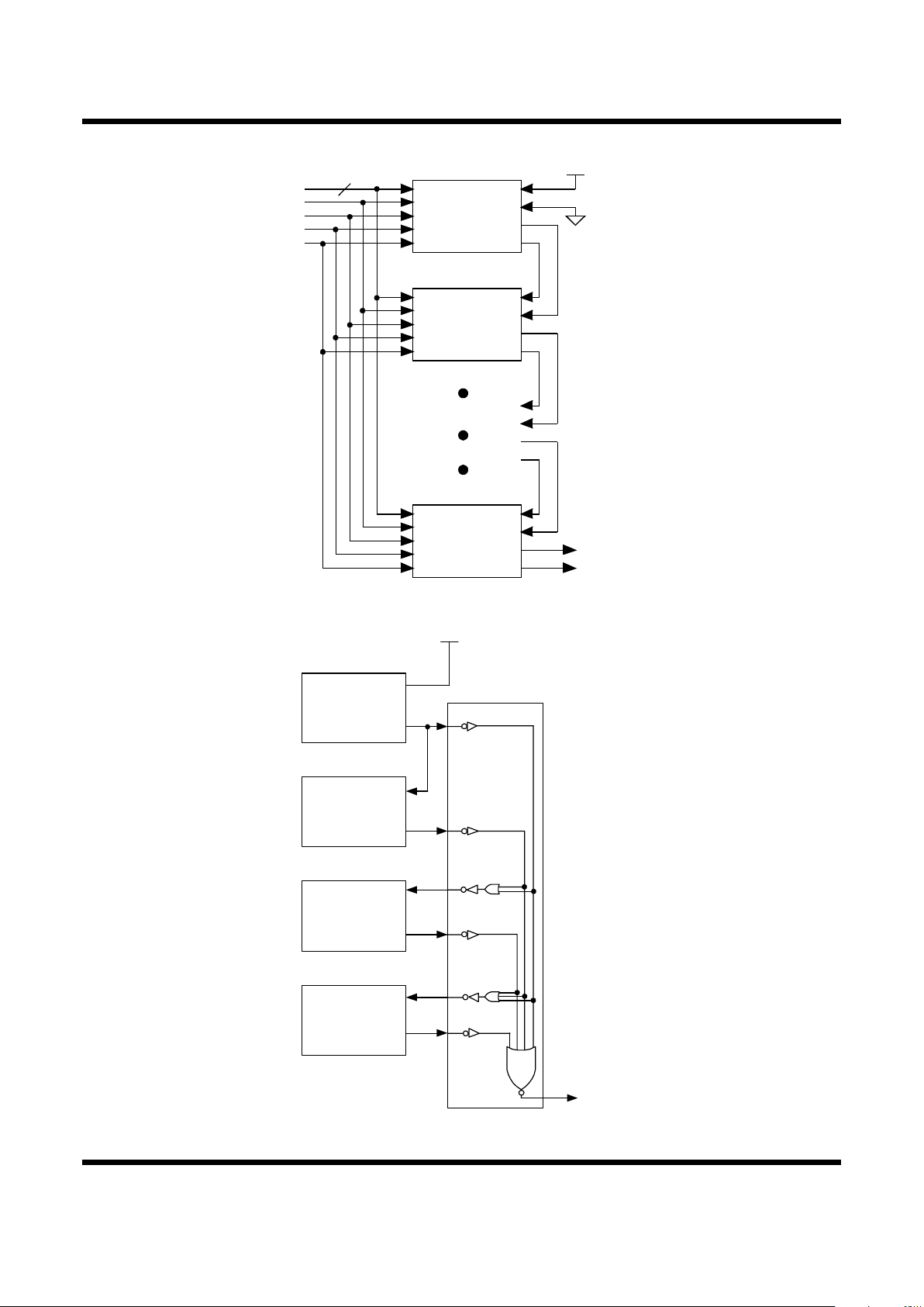
Cascading LANCAMs
A Page Address register in each device simplifies vertical
expansion in systems using more than one LANCAM.
This register is loaded with a specific device address
during system initialization, which then serves as the
higher-order address bits. A Device Select register allows
the user to target a specific device within a vertically
cascaded system by setting it equal to the Page Address
Register value, or to address all the devices in a string at
the same time by setting the Device Select value to
FFFFH.
Figure 4 shows expansion using a daisy chain. Note that
system flags are generated without the need for external
logic. The Page Address register allows each device in the
vertically cascaded chain to supply its own address in the
event of a match, eliminating the need for an external
priority encoder to calculate the complete Match address
at the expense of the ripple-through time to resolve the
Highest-Priority match. The Full flag daisy-chaining
allows Associative writes using a Move to Next Free
Address instruction, which does not need a supplied
address.
Figure 5 shows an external PLD implementation of a
simple priority encoder that eliminates the daisy chain
ripple-through delays for systems requiring maximum
performance from many CAMs.
Page 7
Functional Description LANCAM B Family
Rev. 2 7
Figure 4: Vertical Cascading
Figure 5: External Prioritizing
Vcc
/MI
/FI
/FF
/MF
LANCAM
16
/E
/W
/CM
/EC
DQ15–0
/MI
/FI
/MF
/MI
/FI
/MF
/E
/W
/CM
/EC
DQ15–0
/E
/W
/CM
/EC
DQ15–0
/E
/W
/CM
/EC
DQ15–0
LANCAM
LANCAM
/FF
SYSTEM FULL
SYSTEM MATCH
/FF
/MA
/MA
/MA
/MA
LANCAM
/MI
/MI
/MI
/MI
V
cc
PLD
LANCAM
LANCAM
LANCAM
SYSTEM
MATCH
Page 8

LANCAM B Family Operational Characteristics
8
Rev. 2
OPERATIONAL CHARACTERISTICS
Note: Throughout the following, “aaaH” represents a three-digit hexadecimal number “aaa,” while “bbB” represents a two-digit
binary number “bb.” All memory locations are written to or read from in 16-bit segments. Segment 0 corresponds to the lowest order
bits (bits 15–0) and Segment 3 corresponds to the highest order bits (bits 63–48).
Control Bus
Refer to Figure 1 on page 1 for the following discussion.
The inputs Chip Enable (/E), Write Enable (/W),
Command Enable (/CM), and Enable Daisy Chain (/EC)
are the primary control mechanism for the LANCAM. The
/EC input of the Control bus enables the /MF Match flag
output when LOW and controls the daisy chain operation.
Instructions are the secondary control mechanism. Logical
combinations of the Control Bus inputs, coupled with the
execution of Select Persistent Source (SPS), Select
Persistent Destination (SPD), and Temporary Command
Override (TCO) instructions allow the I/O operations to
and from the DQ15–0 lines to the internal resources, as
shown in Table 2.
The Comparand register is the default source and
destination for Data Read and Write cycles. This default
state can be overridden independently by executing a
Select Persistent Source or Select Persistent Destination
instruction, selecting a different source or destination for
data. Subsequent Data Read or Data Write cycles access
that source or destination until another SPS or SPD
instruction is executed. The currently selected persistent
source or destination can be read back through a TCO PS
or PD instruction. The sources and destinations availab le
for persistent access are those resources on the 64-bit bus:
Comparand register, Mask Register 1, Mask Register 2,
and the Memory array.
The default destination for Command Write cycles is th e
Instruction decoder, while the default source for
Command Read cycles is the Status register.
Temporary Command Override (TCO) instructions
provide access to the Control register, the Page Address
register, the Segment Control register, the Address
register, the Next Free Address register, and Device Select
register. TCO instructions are active only for one
Command Read or Write cycle after being loaded into the
Instruction decoder.
The data and control interfaces to the LANCAM are
synchronous. During a Write cycle, the Control and Data
inputs are registered by the falling edge of /E. When
writing to the persistently selected data destination, the
Destination Segment counter is clocked by the rising edge
of /E. During a Read cycle, the Control inputs are
registered by the falling edge of /E, and the Data outputs
are enabled while /E is LOW. When reading from the
persistently selected data source, the Source Segment
counter is clocked by the rising edge of /E.
The Register Set
The Control, Segment Control, Address, Mask Register 1,
and the Persistent Source and Destination registers are
duplicated, with one set termed the Foreground set and the
other the Background set. The active set is chosen by
issuing Select Foreground Registers or Select Background
Registers instructions. By default, the Foreground set is
active after a reset. Having two alternate sets of registers
that determine the device configuration allows for a rapid
return to a foreground network filtering task from a
background housekeeping task.
Writing a value to the Control register or writing data to
the last segment of the Comparand or either Mask register
causes an automatic comparison to occur between the
contents of the Comparand register and the words in the
CAM segments of the memory marked valid, masked by
MR1 or MR2 if selected in the Control register.
Instruction Decoder
The Instruction decoder is the write-only decode logic for
instructions and is the default destination for Command
Write cycles. If an instruction’s Address Field flag (bit 11)
is set to a 1, it is a two-cycle instruction that is not
executed immediately. For the next cycle only, the data
from a Command Write cycle is loaded into the Address
register and the instruction then completes at that address.
The Address register then increments, decr ements, or stays
at the same value depending on the setting of Control
Register bits CT3 and CT2. If the Ad dres s Fiel d fl ag is not
set, the memory access occurs at the address currently
contained in the Address register.
Control Register (CT)
The Control register contains a number of switches that
configure the LANCAM, as shown in Control Register
Bits on page 23. It is written or read using a TCO CT
instruction. If bit 15 of the value written during a TCO CT
is a 0, the device is reset (and all other bits are ignored).
See Table 3 on page 11 for the Reset states. Bit 15 always
reads back as a 0. A write to the Control register causes an
automatic compare to occur (except in the case of a reset).
Either the Foreground or Background Control register is
active, depending on which register set has been selected,
and only the active Control register is written to or read
from.
If the Mat ch Flag is disabled th rough bit 14 and bit 13, the
internal match condition, /MA(int), used to determine a
daisy-chained device’s response is forced HIGH as shown
in Table 4 so that Case 6 is not possible, effectively
Page 9
Operational Characteristics LANCAM B Family
Rev. 2 9
removing the device from the daisy chain. With the Match
Flag disabled, /MF=/MI and operations directed to
Highest-Priority Match locations are ignored. Normal
operation of the device is with the /MF enabled. The
Match Flag Enable field has no effect on the /MA or /MM
output pins or Status Register bits. These bits always
reflect the true state of the device.
If the Full Flag is disabled through bit 12 and bit 11, the
device behaves as if it is full and ignores instructions to
Next Free address. Also, writes to the Page Address
register are disabled. All other instructions operate
normally. Additionally, with the /FF disabled, /FF=/FI.
Normal operation of the device is with the /FF enabled.
The Full Flag Enable field has no effect on the /FL Status
Register bit. This bit always reflects the true state of the
device.
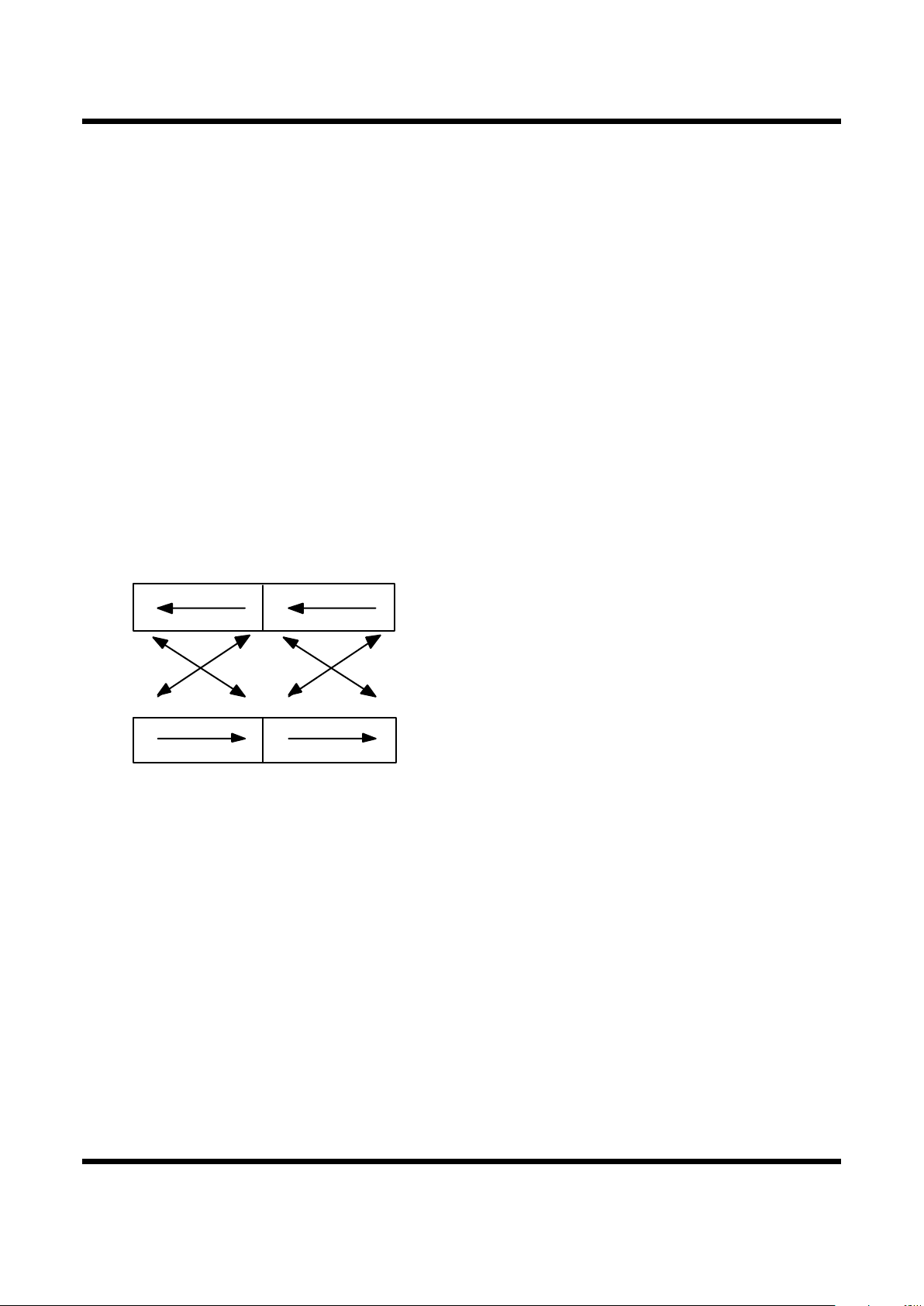
The IEEE Translation control at bit 10 and bit 9 can be
used to enable the translation hardware for writes to 64-bit
resources in the device. When translation is enabled, the
bits are reordered as shown in Figure 6.
Figure 6: IEEE 802.3/802.5 Format Mapping
Control Register bits 8–6 control the CAM/RAM
partitioning. The CAM portion of each word may be sized
from a full 64 bits down to 16 bits in 16-bit increments.
The RAM portion can be at either end of the 64-bit word.
Compare masks may be selected by bit 5 and bit 4. Mask
Register 1, Mask Register 2, or neither may be selected to
mask compare operations. The address register behavior is
controlled by bit 3 and bit 2, and may be set to increment,
decrement, or neither after a memory access. B it 1 and bit
0 set the operating mode: Standard or Enhanced as shown
in Table 4 on page 12. The device resets to the Standard
mode, and follows the op erating respons es of the orig inal
MU9C1480 in Table 4. When operating in Enhanced
mode, it is not necessary to unlock the daisy chain with a
NOP instruction before command or data writes after a
non-matching compare, as required in Standard mode.
Segment Control Register (SC)
The Segment Control register, as shown in Segment
Control Register Bits on page 23, is accessed using a TCO
SC instruction. On read cycles, D15, D10, D5, and D2
always read back as 0s. Either the Foreground or
Background Segment Control register is active, depending
on which register set is selected, and only the active
Segment Control register is written to or read from.
The Segment Control register contains dual independent
incrementing counters with limits, one for data reads and
one for data writes. These count ers control which 16-bit
segment of the 64-bit internal resource is accessed during
a particular data cycle on the 16-bit data bus. The actual
destination for data writes and source for data reads (called
the persistent destination and source) are set independently
with SPD and SPS instructions, respectively.
Each of the two counters consists of a start limit, an end
limit, and the current count value that points to the
segment to be accessed on the next data cycle. The current
count value can be set to any segment, even if it is outside
the range set by the start and end limits. The counters
count up from the current count value to the end li mit and
then jump back to the start limit. If the current co unt is
greater than the end limit, the current count value
increments to three, rolls over to zero, continues
incrementing until the end limit is reached, and then jumps
back to the start limit.
If a sequence of data writes or reads is interrupted, the
Segment Control register can be reset to its initial start
limit values by using an RSC instruction. After the
LANCAM is reset, both Source and Destination counters
are set to count from Segment 0 to Segment 3 with an
initial value of 0.
DQ15 DQ8 DQ7 DQ0
DQ15 DQ8 DQ7 DQ0
Page 10

LANCAM B Family Operational Characteristics
10
Rev. 2
Notes:
1. Default Command Write cycle destination (does not require a TCO instruction).
2. Default Command Write cycle destination (no TCO instruction required) if Address Field flag was set in bit 11 of the instruction loade d in the
previous cycle.
3. Loaded or read on the Command Write or Read cycle immediately following a TCO instruction. Active for one Command Write or Read cycle only.
NFA register can not be loaded this way.
4. Default Command Read cycle source (does not require a TCO instruction).
5. Default Command Read cycle source (does not require a TCO instruction) if the previous cycle was a Command Read of Status Register Bits 15–0.
If next cycle is not a Command Read cycle, any subsequent Command Read cycle accesses the Status Register Bits 15–0.
6. Default persistent source and destination on power-up and after Reset. If other resources were sources or destinations, SPD CR or SPS CR restores
the Comparan d register as the destination or so urce.
7. Selected by executing a Selec t Pe rsist ent Destination instruction.
8. Selected by executing a Sele c t Pe rsist ent Source instruction.
9. Access may require multiple 16-bit R ead or Write cycles. The Se gment C ontrol register controls the selec tion of the de sired 16-bit segment(s) by
establishing the Segment counters’ start and end limits and count va lu es.
10. Device is deselected if Device Select register setting d oes not equal Page A ddress register setting, unless the Device Select Regi ster is set to
FFFFH, which all o ws on ly wr it e acc ess t o t he d evice . ( Writes to the Device Sel ect register are al ways act iv e. ) Devi ce ma y als o be deselected under
locked daisy chain conditions as shown in Table 4.
11. A Command Read cycle after a TCO PS or TCO PD reads back the Instruction decod er bits that were last set to select a persistent source or
destination. The TCO PS instruction also reads back the Device ID.
Table 2: Input/Output Operations
Cycle Type /E /CM /W I/O Status SPS SPD TCO Operation Notes
Cmd Write L L L IN
IN
IN
IN
IN
IN
IN
3
3
3
3
3
Load Instruction decoder
Load Address register
Load Control register
Load Page Address register
Load Segment Control register
Load Device Select register
Deselected
1
2,3
3
3
3
3
10
Cmd Read L L H OUT
OUT
OUT
OUT
OUT
OUT
OUT
OUT
OUT
HIGH-Z
3
3
3
3
3
3
3
Read Next Free Address register
Read Address register
Read Status Register bits 15–0
Read Status Register bits 31–16
Read Control register
Read Page Address register
Read Segment Control register
Read Device Select register
Read Current Persistent Source or Destination
Deselected
3
3
4
5
3
3
3
3
3,11
10
Data Write L H L IN
IN
IN
IN
IN
IN
IN
3
3
3
3
3
3
Load Comparand register
Load Mask Register 1
Load Mask Register 2
Write Memory Array at address
Write Memory Array at Next Free address
Write Memory Array at Highest-Priority match
Deselected
6,9
7,9
7,9
7,9
7,9
7,9
10
Data Read L H H OUT
OUT
OUT
OUT
OUT
HIGH-Z
3
3
3
3
3
Read Comparand register
Read Mask Register 1
Read Mask Register 2
Read Memory Array at address
Read Memory Array at Highest-Priority match
Deselected
6, 9
8, 9
8, 9
8, 9
7, 8
10
H X X HIGH-Z Deselected
Page 11

Operational Characteristics LANCAM B Family
Rev. 2 11
Page Address Register (PA)
The Page Address register is loaded using a TCO PA
instruction followed by a Command Write cycle of a user
selected 16-bit value (not FFFFH). The entry in the PA
register gives a unique address to the different devices in a
daisy chain. In a daisy chain, the PA value of each device
is loaded using the SFF instruction to advance to the next
device, shown in the Setting Page Address Regis ter Values
on page 16. A software reset (using the Control register)
does not affect the Page Address register.
Device Select Register (DS)
The Device Select register selects a specific (target)
device. The TCO DS instruction sets the 16-bit DS register
to the value of the following Command Write cycle. The
DS register can be read. A device is selected when its DS
is equal to its PA value. In a daisy chain, setting DS =
FFFFH selects all devices. However, in this case, the
ability to read information out of the device is restricted as
shown in Table 4. A software reset (using the Control
register) does not affect the Device Select register.
Address Register (AR)
The Address register points to the CAM memory location
to be operated upon when M@[AR] or M@aaaH is part of
the instruction. It can be loaded directly by using a TCO
AR instruction or indirectly by using an instruction
requiring an absolute address, such as MOV aaaH,CR,V.
After being loaded, the Address register value is the next
memory access referencing the Address regis ter. A reset
sets the Address register to zero.
Control Register bits CT3 and CT2 set the Address
register to automatically increment or decrement (or not
change) during sequences of Command or Data cycles.
The Address register changes after executing an
instruction that includes M@[AR] or M@aaaH, or after a
data access to the end limit segment (as set in the Segment
Control register) when the persistent source or destination
is M@[AR] or M@aaaH.
Either the Foreground or Background Address register is
active, depending on which register set is selected, and
only the active Address register is written to or read from.
Next Free Address Register (NF)
The LANCAM automatically stores the address of th e f irst
empty memory location in the Next Free Address register,
which is then used as a memory address pointer for
M@NF operations. The Next Free Address register,
shown in Next Free Address Bits on page 24, can be read
using a TCO NF instruction. By taking /EC LOW during
the TCO NF instruction cycle, only the device with /FI
LOW and /FF HIGH outputs the contents of its Next Free
Address register, giving the Next Free address in a system
of daisy-chained devices. The Next Free address may be
read from a specific device in the chain by setting the
Device Select register to the value of the desired device’s
Page address and leaving /EC HIGH. The Full Flag daisy
chain causes only the device whose /FI input is LOW and
/FF output HIGH to respond to an instruction using the
Next Free address. After a reset, the Next Free Address
register is set to zero.
Table 3: Device Control State After Reset
CAM Status /RESET Cond ition
Validity bits at all memory locations
Match and Full Flag outputs
IEEE 802.3–802.5 Input Translation
CAM/RAM Partitioning
Comparison Masking
Address register auto-increment or auto-decrement
Source and Destination Segment counters count ranges
Address register and Next Free Address register
Page Address and Device Select registers
Control register after reset (including CT15)
Persistent Destination for Command writes
Persistent Source for Command reads
Persistent Source and Destination for Data reads and writes
Operating Mode
Configuration Register set
Skip = 0, Empty = 1 (empty)
Enabled
Not translated
64 bits CAM, 0 bits RAM
Disabled
Disabled
00B to 11B; loaded with 00B
Contain all 0s
Contain all 0s (no change on software reset)
Contains 0008H
Instruction decoder
Status register
Comparand register
Standard
Foreground
Page 12

LANCAM B Family Operational Characteristics
12
Rev. 2
Notes:
1. Exceptions are:
A) A write to the Device Select register is always active in all devices;
B) A write to the Page Address register is active in the device with /FI LOW an d /F F HI GH ; and
C) The Set Full Flag (SFF) ins tr u ction is activ e in the device with /FI LOW and /FF HIGH.
2. If /MF is disabled in the Control register, In ternal /MA is forced HIGH preventing a Case 6 response.
3. This is NO for a MOV instruction involving M emory at Next Free address if /FI is HIGH or the device is full.
4. This is NO if the Persist en t Des ti na tion is Memory at Next Free address and /FI is HIGH or the dev ice is full.
5. For a Command read following a TCO NF instruction, this is YES if the device contains the first empty location in a daisy chain (i.e., /FI LOW and
/FF HIGH) and NO if it does not.
6. This is NO for a MOV or VBC instruction involving Memory at Highest-Priority match.
7. This is NO if the Persist en t Destination is Memory at Highest-Priority match.
Status Register
The 32-bit Status reg ister, shown in Status Register Bits on
page 24, is the default source for Command Read cycles.
Bit 31 (internal Full flag) goes LOW if the particular
device has no empty memory locations. Bit 30 is the
internal Multiple Match flag, which goes LOW if a
Multiple match was detected. Bit 29 and Bit 28 are the
Validity bits, which reflect the validity o f the last memory
location read. After a reset, the Validity bits read 11 until a
read or move from memory has occurred. The rest of the
Status register down to bit 1 cont ains the Page address of
the device and the address of the Highest-Priority match.
After a reset or a no-match condition, the match address
bits are all 1s. Bit 0 is the internal Match flag, which goes
LOW if a match was found in this particular device.
Comparand Register (CR)
The 64-bit Comparand register is the default destination
for data writes and reads, using the Segment Control
register to select which 16-bit segment of the Comparand
register is to be loaded or read out. The persistent source
and destination for data writes and reads can be changed to
the Mask registers or memory by SPS and SPD
instructions. During an automatic or forced compare, the
Comparand register is simultaneously compared against
the CAM portion of all memory locations with the correct
validity condition. Automatic compares always compare
against valid memory locations, while forced compares,
using CMP instructions, can compare against memory
locations tagged with any specific validity condition.
The Comparand register may be shifted one bit at a time to
the right or left by issuing a Shift Right or Shift Left
instruction, with the right and left limits for the
wrap-around determined by the CAM/RAM partitioning
Table 4: Standard and Enhanced Mode Device Select Response
Standard Mode
Case Internal
/EC(int)
Internal
/MA(int)
External
/MI
Device Select
Register
Command
Write
1
Data
Write
Command
Read
Data
Read
1 1 X X DS = FFFFH
YES
3
YES
4
NO NO
2 1 X X DS = PA
YES
3
YES
4
YES YES
31 X XDS ≠ FFFFH and
DS ≠ PA
NO NO NO NO
40 X 0 X NONO
NO
5
NO
50 1 1 X NONO
NO
5
NO
6
2
001 X
YES
3
YES
4
YES
5
YES
Enhanced Mode
Case Internal
/EC(int)
Internal
/MA(int)
External
/MI
Device Select
Register
Command
Write
1
Data
Write
Command
Read
Data
Read
1 1 X X DS = FFFFH
YES
3
YES
4
NO NO
2 1 X X DS = PA
YES
3
YES
4
YES YES
31 X XDS ≠ FFFFH and
DS ≠ PA
NO NO NO NO
40 0 0 X
YES
3,6
YES
3,7
NO
5
NO
50 1 X X
YES
3,6
YES
3,7
NO
5
NO
6
2
001 X
YES
3
YES
4
YES
5
YES
Page 13

Operational Characteristics LANCAM B Family
Rev. 2 13
set in the Control register. During shift rights, bits shifted
off the LSB of the CAM partition reappear at the MSB of
the CAM partition. Likewise, bits shifted off the MSB of
the CAM partition reappear at the LSB during shift lefts.
Mask Registers (MR1, MR2)
The Mask registers can be used in two different ways:
either to mask compares or to mask data writes and moves.
Either Mask register can be selected in the Control register
to mask every compare, or selected by instructions to
participate in data writes or moves to and from Memory. If
a bit in the selected Mask register is set to a 0, the
corresponding bit in the Comparand register enters into a
masked compare operation. If a Mask bit is a 1, the
corresponding bit in the Comparand regi ster does not enter
into a masked compare operation. Bits set to 0 in the Mask
register cause correspo ndi n g b its in t he des t inat ion register
or memory location to be updated when masking data
writes or moves, while a bit set to 1 prevents that bit in the
destination from being changed.
Either the Foreground or Background MR1 can be set
active, but after a reset, the Foreground MR1 is active by
default. MR2 incorporates a sliding mask, where the data
can be replicated one bit at a time to the right or left with
no wrap-around by issuing a Shift Right or Shift Left
instruction. The right and left limits are determined by the
CAM/RAM partitioning set in the Control register. For a
Shift Right the upper limit bit is replicated to the next
lower bit, while for a Shift Left the lower limit bit is
replicated to the next higher bit.
The Memory Array
Memory Organization
The Memory array is organized into 64-bit words with
each word having an additional two validity bits. By
default, all words are configured to be 64 CAM cells.
However, bits 8–6 of the Control register can divide each
word into a CAM field and a RAM field. The RAM field
can be assigned to the least-significant or most-significant
portion of each entry.
The CAM/RAM partitioning is allowed on 16-bit
boundaries, permitting selection of the configuration
shown in Control Register Bits on page 23, bits 8–6 (e.g.,
“001” sets the 48 MSBs to CAM and the 16 LSBs to
RAM). Memory Array bits designated as RAM can be
used to store and retrieve dat a associated wit h the CAM
content at the same memory location.
Memory Access
There are two general ways to get data into and out of the
Memory array: directly or by movi ng th e data by means of
the Comparand or Mask registers.
The first way, through direct reads or writes, is set up by
issuing a Set Persistent Destination (SPD) or Set Persistent
Source (SPS) command. The addresses for the direct
access can be supplied directly; supplied from the Address
register, supplied from the Next Free Address register, or
supplied as the Highest-Priority Match address.
Additionally, all the direct writes can be masked by either
Mask register.
The second way is to move data by means of the
Comparand or Mask registers. This is accomplished by
issuing Data Move commands (MOV). Moves using the
Comparand register can also be masked by either of the
Mask registers.
Figure 7: Read Cycle
/E
DQ15-0
/W
/CM
/EC
DATA OUT
Page 14

LANCAM B Family Operational Characteristics
14
Rev. 2
Figure 8: Write Cycle
Figure 9: Cycle-to-Cycle Timing Example
I/O Cycles
The LANCAM supports four basic I/O cycles: Data Read,
Data Write, Command Read, and Command Write. The
states of the /W and /CM control inputs det ermi n e the type
of cycle. These signals are registered at the beginning of a
cycle by the falling edge of /E. Table 1 on page 3 shows
how the /W and /CM signals select the cycle type.
During Read cycles, the DQ15–0 outputs are enabled after
/E goes LOW. During Write cycles, the data or command
to be written is captured from DQ15–0 at the beginning of
the cycle by the falling edge of /E. Figure 10 on page 15
and Figure 7 on page 13, show Read and Write cycles
respectively. Figure 8 on page 14, shows typical
cycle-to-cycle timing with the Match flag valid at the end
of the Comparand Write. Data writes and reads to the
comparand, Mask registers, or memory occur in one to
four 16-bit cycles, depending on the settings in the
Segment Control register. The Compare operation
automatically occurs during Data writes to the Comparand
or Mask registers when the destination segment counter
reaches the end count set in the Segment Co ntrol register.
If there was a match, the second cycle reads status or
associated data, depending on the state of /CM. For
cascaded devices, /EC needs to be LOW at the start of the
cycle prior to any cycle that requires a locked daisy chain,
such as a Status register or associated data read after a
match. If there is no match in Standard mode, the output
buffers stay High-Z, and the daisy chain must be unlocked
by taking /EC HIGH during a NOP or other
non-functioning cycle, as indicated in Table 4 on page 12.
Figure 9 on page 14 shows how the internal /EC timing
holds the daisy chain locking effect over into the next
cycle. In Enhanced mode, this NOP is not needed before
data or command writes following a non-matching
compare, as indicated by Table 4 on page 12. A
single-chip system does not require daisy-chained match
flag operation, hence /EC could be tied HIGH and the
/MA pin or flag in the Status register used instead of /MF,
allowing access to the device regardless of the match
condition.
The minimum timings for the /E control signal are given
in Table 9 on page 27. Note that at minimum timin gs the
/E signal is non-symmetrical and that different cycle types
have different ti ming requirements, as given in Table 6 on
page 22.
DQ15–0
/W
/CM
/E
/EC
ASSOCIATED DATA
READ CYCLE
/MA AND /MM FLAGS UPDATED
DATA
MATCH FLAG VALID
DQ15–0
/W
/CM
/MA, /MM
/EC
/MF
/E
COMPARAND WRITE
CYCLE
STATUS READ
CYCLE
DATA DATA
Page 15

Operational Characteristics LANCAM B Family
Rev. 2 15
Compare Operations
During a Compare operation, the data in the Comparand
register is compared to all locations in the Memory array
simultaneously. Any Mask register used during compares
must be selected beforehand in the Control register. There
are two ways compares are initiated: Automatic compare
and Forced compare.
Automatic compares perform a compare of the contents of
the Comparand register against Memory locations t hat are
tagged as “Valid,” and occur whenever the following
happens:
• The Destination Segment counter in the Segment
Control register reaches its end limit during writes to
the Comparand or Mask registers.
• After a command write of a TCO CT is executed
(except for a software reset), so that a compare is
executed with the new settings of the Control register.
Forced compares are initiated by CMP instructions using
one of the four validity conditions: V, R, S, and E. The
forced compare against “Empty” locations automatically
masks all 64 bits of data to find all locations with the
validity bits set to “Empty,” while the other forced
compares are only masked as selected in the Control
register.
Vertical Cascading
LANCAMs can be vertically cascaded to increase system
depth. Through the use of flag daisy-chaining, multiple
devices respond as an integrated system. The flag daisy
chain allows all commands to be issued globally, wi th a
response only in the device containing the Highest-Priority
Matching or Next Free location. When connected in a
daisy chain, the last device’s Full flag and Match flag
accurately report the condition for the whole string. A
system in which LANCAMs are vertically cascaded using
daisy-chaining of the flags is shown in Figure 4 on page 7.
To operate the daisy chain, the Device Select registers are
set to FFFFH to enable all devices to execute Command
Write and Data Write cycles. In normal operation, read
cycles are enabled from the device with the
Highest-Priority match by locking the daisy chain (see the
Locked Daisy Chain section). An individual device in the
chain may be targeted for a read or write operation by
temporarily setting the Device Select registers to the Page
address of the target device. Setting the Device Select
registers back to FFFFH restores the operation of the
entire daisy chain.
Match Flag Cascading
The Match Flag daisy chain cascading has three purposes:
first, to allow operations on Highest-Priority Match
addresses to be issued globally over the whole string;
second, to provide a sy stem wide match flag; third, to lock
out all devices except the one with the Highest-Priority
match for instructions such as Status reads after a match.
The Match flag logic causes only the highest-priority
device to operate on its Highest-Priority Match location
while devices with lower-priority matches ignore
Highest-Priority Match operations. The lock-out feature is
enabled by the match flag cascading and the use of the /EC
control signal, as shown in Table 4.
The ripple delay of the flags when connect ed in a daisy
chain requires the extension of the /E HIGH time until the
logic in all devices has settled out. In a string of “n”
devices, the /E HIGH time should be greater than
If the last device’s Match flag is required by external logic
or a state machine before the start of the next CAM cycle,
one additional tMIVMFV should be added to the /E HIGH
time along with the setup time and delays for the external
logic.
Figure 10: /EC (Int) Timing Diagram
Locked Daisy Chain
In a locked daisy chain, the highest-pri ority device is the
one with /MI HIGH and /MF LOW. In Standard mode,
only this device responds to command and data reads and
writes, until the daisy chain has been unlocked by taking
/EC HIGH. This allows reading the associated data field
from only the Highest-Priority Match location anywhere
in a string of devices, or the Mat ch ad dres s fro m t he S t atus
register of the device with the match. It also permits
updating the entry stored at the Highest-Priority Match
location. In Enhanced mode, devices are enabled to
respond to some command and data writes, as noted in
Table 4 on page 12, but not command and data reads.
Table 4 (Standard and Enhanced modes) show when a
device responds to reads or writes and when does not,
based on the state of /EC(int), the internal match
condition, and other control inputs. /EC is latched by the
falling edge of /E. /EC(int) is registered from the latched
/EC signal off the rising edge of /E, so it controls what
happens in the next cycle, as shown in Figure 10 on page
tEHMFV + (n-2)
· tMIVMFV
/E
/EC
/EC (INT)
/MF
Page 16

LANCAM B Family Operational Characteristics
16
Rev. 2
15. When /EC is first taken LOW in a string of LANCAM
devices (and assuming the Device Select registers are set
to FFFFH), all devices respond to that comma nd write or
data write.
From then on the daisy chain remains locked in each
subsequent cycle as long as /EC is held LOW on the
falling edge of /E in the current cycle. When the daisy
chain is locked in Standard mode, only the
Highest-Priority Match device responds (See Case 6 of
Table 4). If, for example, all of the CAM memory
locations were empty, there would be no match, and /MF
would stay HIGH. Since none of the devices could then be
the Highest-Priority Match device, none respond to reads
or writes until the daisy chain is unlocked by taking /EC
HIGH and asserting /E for a cycle.
If there is a match between the data in the Comparand
register and one or more locations in memory, then only
the Highest-Priority Match device responds t o any cycle,
such as an associated data or Status Register read. If there
is not a match, then a NOP with /EC HIGH needs t o be
inserted before issuing any new instructions, such as Write
to Next Free Address instruction to learn the data. Since
Next Free operations are controlled by the /FI–/FF daisy
chain, only the device with the first empty location
responds. If an instruction is used to unlock the daisy
chain, it works only on the Highest-Priority Match device,
if one exists. If none exists, the instruction has no effect
except to unlock the daisy chain. To read the Status
registers of specific devices when there is no match
requires the use of the TC O D S command to set DS=PA of
each device. Single chip systems can tie /EC HIGH and
read the Status register or the /MA and /MM pins to
monitor match conditions, as the daisy chain lock-out
feature is not needed in this configuration. This removes
the need to insert a NOP in the case of a no-match.
When the Control register is set to Enhanced mode, you
can continue to write data to the Comparand register or
issue a Move to Next Free Address instruction without
first having to issue a NOP with /EC HIGH to un lock the
daisy chain after a Compare cycle with no match, as
indicated in cases 4 and 5 of Table 4 on page 12. In
Enhanced mode, data write cycles as well as command
write cycles are enabled in all devices even when /EC is
LOW. Exceptions are data writes, moves, or VBC
instructions involving HM, which occur only in the device
with the highest match; and data writes or move
instructions involvi ng NF, which occur only in the device
with /FI LOW and /FF HIGH. Enhanced mode speeds up
system performance by eliminating the need to unlock the
daisy chain before Command or Data Write cycles.
Full Flag Cascading
The Full Flag daisy chain cascading has the following
three purposes:
• Allow instructions that address Next Free locations to
operate globally
• Provide a system wide Full flag
• Allow the loading of the Page Address registers
during initialization using the SFF instruction
The full flag logic causes only the device containing the
first empty location to respond to Next Free instructions
such as MOV NF,CR ,V, which moves the contents of the
Comparand register to the first empty location in a string
of devices and sets that location Valid , making it av ailable
for the next automatic compare. W ith dev ices connected as
in Figure 4 on page 7, the /FF output of the last device in a
string provides a full indication for the entire string.
IEEE 802.3/802.5 Format Mapping
To support the symmetrical mapping between the address
formats of IEEE 802.3 and IEEE 802.5, the LANCAM
provides a bit translation facility. Formally expressed, the
nth input bit, D(n), maps to the xth output bit, Q(x),
through the following expressions:
Setting Control Register bit 10 and bit 9 selects whether to
persistently translate, or persistently not to translate, the
data written onto the 64-bit internal bus. The default
condition after a Reset command is not to translate the
incoming data. Figure 6 on page 9 shows the bit mappi ng
between the two formats.
Initializing the Lancam
Initialization of the LANCAM is required to configure the
various registers on the device. Since a Control register
reset establishes the operating conditions shown in T able 3
on page 11, restoration of operating conditions better
suited for the application may be required after a reset,
whether using the Control Register reset, or the /RESET
pin. When the device powers up, the memory an d r egisters
are in an unknown state, so the /RESET pin must be
asserted to place the device in a known state.
Setting Page Address Register Values
In a vertically cascaded system, the user must set the
individual Page Address registers to unique values by
using the Page Address initialization mechanism. Each
Page Address register must contain a unique value to
prevent bus contention. This process allows individual
device selection. The Page Address register initialization
works as follows: Writes to Page Address registers are
only active for devices with /FI LOW and /FF HIGH. At
D(n) = Q(7–n) for 0 <
n < 7,
D(n) = Q(23–n) for 8 <
n < 15
Page 17

Operational Characteristics LANCAM B Family
Rev. 2 17
initialization, all devices are empty, thus the top device in
the string responds to a TCO PA instruction, and loads its
PA register. A Set Full Flag (SFF) instruction advances to
the next device in the string and is active only for the
device with /FI LOW and /FF HIGH. The SFF instruction
changes the first device’s /FF to LOW, although the device
really is empty, which allows the next device in the string
to respond to the TCO PA instruction and load its PA
register. The initialization proceeds through the chain in a
similar manner filling all the PA registers in turn. Each
device must have a uniq ue Page A ddress value stored in
its PA register, or contention results. After all the PA
registers are filled, the entire string is reset through the
Control register, which does not change the values stored
in the individual PA registers. After the reset, the Device
Select registers usually are set to FFFFH to enable
operation in Case 1 of Table 4 on page 1 2. The Control
registers and the Segment Control registers are then set to
their normal operating values for the application.
Vertically Cascaded System Initialization
Table 5 shows an example of code that initializes a
daisy-chained string of LANCAM devices. The
initialization example shows how to set the Page Address
registers of each of the devices in the chain through the
use of the Set Full Flag instruction, and how the Co ntrol
registers and Segment counters of all the LANCAM
devices are set for a typical application. Each Page
Address register must contain a unique value (not FFFFH)
to prevent bus contention.
For typical daisy chain operation, data is loaded into the
Comparand registers of all the devices in a string
simultaneously by setting DS=FFFFH. Since reading is
prohibited when DS=FFFFH (except for the device with a
match), for a diagnostic operation you need to select a
specific device by setting DS=PA for the desired device to
be able to read from it. Refer to Table 4 on page 12 for
preconditions for reading and writing. Initialization for a
single LANCAM is similar. The Device Select register in
this case is usually set to equal the Page Address register
for normal operations. Also, the dedicated /MA flag output
can be used instead of /MF, allowing /EC to be tied HIGH.
Notes:
1. T oggling the /RESET pin generates the same effect as this reset of the Control register , but good programming practice dictates a software reset for
initialization to account for all possible pri or con diti ons.
2. This instruction may be omitted for a single LANCA M application.
3. The last SFF causes the /FF pin in the last chip in a da isy chain to go LOW. In a daisy chain, DS needs to be set equal to PA to read out a
particular chip prior to a match conditi on.
4. A typical LANCAM c ontrol environment: Enable match flag; Ena ble full flag; 48 CAM bits, 16 RAM bits; Disable com parison masking; and
Enable address increment. See Table on page 23 for Control Register bit assignments.
Table 5: Initialization Routine Example
Cycle Type Op-Code
on DQ Bus
Control Bus Comments Notes
/E /CM /W /EC
Command read
Command write
Command write
Command write
Command write
Command write
Command write
Command write
Command write
Command write
Command write
Command write
Command write
Command write
Command write
TCO DS
FFFFH
TCO CT
0000H
TCO PA
nnnnH
SFF
TCO CT
0000H
TCO CT
8040H
TCO SC
3808H
SPS M@HM
L
L
L
L
L
L
L
L
L
L
L
L
L
L
L
L
L
L
L
L
L
L
L
L
L
L
L
L
L
L
H
L
L
L
L
L
L
L
L
L
L
L
L
L
L
H
H
H
H
H
H
H
H
H
H
H
H
H
H
H
Clear power-up anomalies
Target Device Select register to disable local device selection.
Disable Device Select feature.
Target Control register for reset.
Causes Reset.
Target Page Address register to set page for cascaded operation.
Page Address value.
Set Full flag; allows access to next device (repeat previous
two cycles plus this one for each device in chain.
Target Control register for reset of Full flags, but not Page address.
Causes Reset.
Target Control register for initial values.
Control register value.
Target Segment Count Control register
Set both Segment counters to write to Segment 1, 2, and 3, and
read from Segment 0.
Set Data reads from Segment 0 of the Highest-Priority match
1
2
2
2,3
1
1
4
4
4
Page 18

LANCAM B Family Instruction Set Descriptions
18
Rev. 2
INSTRUCTION SET DESCRIPTIONS
Notes: Instruction cy cl e le ng ths gi ven i n Table 6 on page 22. If f=1, the instructio n requires an absolute address to be suppli ed on the
following cycle as a Command write. The value sup plied on the second cycle of the instruction updates the ad dress register. After
operations involving M@[AR] or M@aaaH, the Address register increments or decrements depending on the setting in the Control
register.
Instruction: Select Persistent Source (SPS)
Binary Op-Code: 0000 f000 0000 0sss
f Address Field flag
sss Selected source
This instruction selects a persistent source for data reads,
until another SPS instruction changes it or a reset occurs.
The default source after reset for Data Read cycles is the
Comparand register. Setting the persistent source to
M@aaaH loads the Address register with “aaaH” and the
first access to that persistent source is at aaaH, after which
the AR value increments or decrements as set in the
Control register. The SPS M@[AR] instruction does the
same except the current Address Register value is used.
Instruction: Select Persistent Destination (SPD)
Binary Op-Code: 0000 f001 mmdd dvvv
f Address Field flag
mm Mask Register select
ddd Selected destination
vvv Validity setting for Memory Location
destinations
This instruction selects a persistent destination for data
writes, which remains until another SPD instruction
changes it or a reset occurs. The default destination for
Data Write cycles is the Comparand register after a reset.
When the destination is the Comparand register or the
Memory array, the data written m ay be masked by either
Mask Register 1 or Mask Register 2, so that only
destination bits corresponding to bits in the Mask register
set to 0 are modified. An automatic compare occurs after
writing the last segment of the Comparand or Mask
registers, but not after writing to Memory. Setting the
persistent destination to M@aaaH loads the Address
register with “aaaH,” and the first access to that persistent
destination is at aaaH, after which the AR value
increments or decrements as set in the Control register.
The SPD M@[AR] instruction does the same except the
current Address Register value is used.
Instruction: Temporary Command Override (TCO)
Binary Op-Code: 0000 0010 00dd d000
ddd Register selected as source or
destination for only the next
Command Read or Write cycle
The TCO instruction selects a register as the source or
destination for only the next Command Read or Write
cycle, so a value can be loaded or read out of the register.
Subsequent Command Read or Write cycles revert to
reading the Status register and writing to the Instruction
decoder. All registers but the NF, PS, and PD can be
written to, and all can be read from. The Status register is
only available through non-TCO Command Read cycles.
Reading the PS register also outputs the Device ID on bits
15–4 as shown in Persistent Source Register Bits on page
24.
Instruction: Data Move (MOV)
Binary Op-Code: 0000 f011 mmdd dsss or
0000 f011 mmdd dvss
f Address Field flag
mm Mask Register select
ddd Destination of data
sss Source of data
v Validity setting if destination is a
Memory location
The MOV instruction performs a 64-bit move of the data
in the selected source to the selected destination. If the
source or destination is aaaH, the Address register is set to
“aaaH.” For MOV instructions to or from aaaH or [AR],
the Address register increments or decrements from that
value after the move completes, as set in the Control
register. D ata transfers between the Memory array and the
Comparand register may be masked by either Mask
Register 1 or Mask Register 2, in which case, only those
bits in the destination that correspond to bits in the
selected Mask register set to 0 are changed. A Memory
location used as a destination for a MOV instruction may
be set to Valid or left unchanged. If the source and
destination are the same register, no net change occurs (a
NOP).
Page 19

Instruction Set Descriptions LANCAM B Family
Rev. 2 19
Instruction: Validity Bit Control (VBC)
Binary Op-Code: 0000 f100 00dd dvvv
f Address Field flag
ddd Destination of data
vvv Validity setting for Memory location
The VBC instruction sets the Validity bits at the selected
memory locations to the selected state. This feature can be
used to find all valid entries by using a repetitive sequence
of CMP V through a mask of all 1s followed by a VBC
HM, S. If the VBC target is aaaH, the Address register is
set to “aaaH.” For VBC instructions t o or from aaaH or
[AR], the Address register increments or decrements from
that value after the operation completes, as set in the
Control register.
Instruction: Compare (CMP)
Binary Op-Code: 0000 0101 0000 0vvv
vvv Validity condition
A CMP V, S, or R instruction forces a Comparison of
Valid, Skipped, or Random entries against the Comparand
register through a Mask register, if one is selected. During
a CMP E instruction, the compare is only done on the
Validity bits and all data bits are automatically masked.
Instruction: Special Instructions
Binary Op-Code: 0000 0110 00dd drrr
ddd Target resource
rrr Operation
These instructions are a special set for the LANCAM to
accommodate the added features over the MU9C1480.
Two alternate sets of configuration registers can be
selected by using the Select Foreground and Select
Background Registers instructions. Thes e registers are the
Control, Segment Control, Address, Mask Register 1, and
the PS and PD registers.
An RSC instruction resets the Segment Control register
count values for both the Destination and Source counters
to the original Start limits.
The Shift instructions shift the designated register one bit
right or left. The right and left limits for shifting are
determined by the CAM/RAM partitioning set in the
Control register. The Comparand register is a
barrel-shifter, and fo r the example of a device set to 64 bits
of CAM executing a Shift Comparand Right instruction,
bit 0 is moved to bit 63, bit 1 is moved to bit 0, and bit 63
is moved to bit 62. For a Shift Comparand Left instruction,
bit 63 is moved to bit 0, bit 0 is moved to bit 1, and bit 62
is moved to bit 63. MR2 acts as a sliding mask, where for
a Shift Right instruction bit 1 is moved to bit 0, while bit 0
“falls off the end,” and bit 63 is repl icated to bit 62. For a
Shift Mask Left instruction, bit 0 is replicated to bit 1, bit
62 is moved to bit 63, and bit 63 “falls off the end.” With
shorter width CAM fields, the bit limits on the right or left
move to match the width of CAM field.
Instruction: Set Full Flag (SFF)
Binary Op-Code: 0000 0111 0000 0000
The SFF instruction is a special instruction used to force
the Full flag LOW to permit setting the Page Address
register in vertically cascaded systems.
Instruction: No Operation (NOP)
Binary Op-Code: 0000 0011 0000 0000
The NOP (No-OP) belongs to the MOV instructions,
where a register is moved to itself. No change occurs
within the device. This instruction is useful in unlocking
the daisy chain in Standard mode.
Page 20

LANCAM B Family Instruction Set Summary
20
Rev. 2
INSTRUCTION SET SUMMARY
Mnemonic Format: INS dst, src[msk], val
INS: Instruction mnemonic
dst: Destination of the data
src: Source of the data
msk: Mask register used
val: Validity condit ion set at the location written
Instruction: Select Persistent Source
Operation Mnemonic Op-Code
Comparand Register SPS CR 0000H
Mask Register 1 SPS MR1 0001H
Mask Register 2 SPS MR2 0002H
Memory Array at Addr. Reg. SPS M@[AR] 0004H
Memory Array at Address SPS M@aaaH 0804H
Mem. at Highest-Priority Match SPS M@HM 0005H
Instruction: Select Persistent Destination
Operation Mnemonic Op-Code
Comparand Register SPD CR 0100H
Masked by MR1 SPD CR[MR1] 0140H
Masked by MR2 SPD CR[MR2] 0180H
Mask Register 1 SPD MR 0108H
Mask Register 2 SPD MR2 0110H
Mem. at Addr. Reg. set Valid SPD M@[AR],V 0124H
Masked by MR1 SPD M@[AR][MR1],V 0164H
Masked by MR2 SPD M@[AR][MR2],V 01A4H
Mem. at Addr. Reg. set Empty SPD M@[AR],E 0125H
Masked by MR1 SPD M@[AR][MR1],E 0165H
Masked by MR2 SPD M@[AR][MR2],E 01A5H
Mem. at Addr. Reg. set Skip SPD M@[AR],S 0126H
Masked by MR1 SPD M@[AR][MR1],S 0166H
Masked by MR2 SPD M@[AR][MR2],S 01A6H
Mem. at Addr.Reg. set Random SPD M@[AR],R 0127H
Masked by MR1 SPD M@[AR][MR1],R 0167H
Masked by MR2 SPD M@[AR][MR2],R 01A7H
Memory at Address set Valid SPD M@aaaH,V 0924H
Masked by MR1 SPD M@aaaH[MR1],V 0964H
Masked by MR2 SPD M@aaaH[MR2],V 09A4H
Memory at Address set Empty SPD M@aaaH,E 0925H
Masked by MR1 SPD M@aaaH[MR1],E 0965H
Masked by MR2 SPD M@aaaH[MR2],E 09A5H
Memory at Address set Skip SPD M@aaaH,S 0926H
Masked by MR1 SPD M@aaaH[MR1],S 0966H
Masked by MR2 SPD M@aaaH[MR2],S 09A6H
Memory at Address set Random SPD M@aaaH,R 0927H
Masked by MR1 SPD M@aaaH[MR1],R 0967H
Masked by MR2 SPD M@aaaH[MR2],R 09A7H
Mem. at Highest-Prio. Match, Valid SPD M@HM,V 012CH
Masked by MR1 SPD M@HM[MR1],V 016CH
Masked by MR2 SPD M@HM[MR2],V 01ACH
Mem. at Highest-Prio. Match, Emp. SPD M@HM,E 012DH
Masked by MR1 SPD M@HM[MR1],E 016DH
Masked by MR2 SPD M@HM[MR2],E 01ADH
Mem. at Highest-Prio. Match, Skip SPD M@HM,S 012EH
Masked by MR1 SPD M@HM[MR1],S 016EH
Masked by MR2 SPD M@HM[MR2],S 01AEH
Mem. at High.-Prio. Match, Random
SPD M@HM,R 012FH
Masked by MR1 SPD M@HM[MR1],R 016FH
Masked by MR2 SPD M@HM[MR2],R 01AFH
Mem. at Next Free Addr., Valid SPD M@NF,V 0134H
Masked by MR1 SPD M@NF[MR1],V 0174H
Masked by MR2 SPD M@NF[MR2],V 01B4H
Mem. at Next Free Addr., Empty SPD M@NF,E 0135H
MaskedbyMR1 SPD M@NF[MR1],E 0175H
MaskedbyMR2 SPD M@NF[MR2],E 01B5H
Mem. at Next Free Addr., Skip SPD M@NF,S 0136H
Masked by MR1 SPD M@NF[MR1],S 0176H
Masked by MR2 SPD M@NF[MR2],S 01B6H
Mem. at Next Free Addr., Random SPD M@NF,R 0137H
Masked by MR1 SPD M@NF[MR1],R 0177H
Masked by MR2 SPD M@NF[MR2],R 01B7H
Instruction: Temporary Command Override
Operation Mnemonic Op-Code
Control Register TCO CT 0200H
Page Address Register TCO PA 0208H
Segment Control Register TCO SC 0210H
Read Next Free Address TCO NF 0218H
Address Register TCO AR 0220H
Device Select Register TCO DS 0228H
Read Persistent Source TCO PS 0230H
Read Persistent Destination TCO PD 0238H
Instruction: Data Move
Operation Mnemonic Op-Code
Comparand Register from:
No Operation NOP 0300H
Mask Register 1 MOV CR,MR1 0301H
Mask Register 2 MOV CR,MR2 0302H
Memory at Address Reg. MOV CR,[AR] 0304H
Masked by MR1 MOV CR,[AR][MR1] 0344H
Masked by MR2 MOV CR,[AR][MR2] 0384H
Memory at Address MOV CR,aaaH 0B04H
Masked by MR1 MOV CR,aaaH[MR1] 0B44H
Masked by MR2 MOV CR,aaaH[MR2] 0B84H
Mem. at Highest-Prio. Match MOV CR,HM 0305H
MaskedbyMR1 MOV CR,HM[MR1] 0345H
MaskedbyMR2 MOV CR,HM[MR2] 0385H
Mask Register 1 from:
Comparand Register MOV MR1,CR 0308H
No Operation NOP 0309H
Mask Register 2 MOV MR1,MR2 030AH
Memory at Address Reg. MOV MR1,[AR] 030CH
Memory at Address MOV MR1,aaaH 0B0CH
Mem. at Highest-Prio. Match MOV MR1,HM 030DH
Instruction: Select Persistent Destination (contin-
Operation Mnemonic Op-Code
Page 21

Instruction Set Summary LANCAM B Family
Rev. 2 21
Mask Register 2 from:
Comparand Register MOV MR2,CR 0310H
Mask Register 1 MOV MR2,MR1 0311H
No Operation NOP 0312H
Memory at Address Reg. MOV MR2,[AR] 0314H
Memory at Address MOV MR2,aaaH 0B14H
Mem. at Highest-Prio. Match MOV MR2,HM 0315H
Memory at Address Register, No Change to Validity bits, from:
Comparand Register MOV [AR],CR 0320H
Masked by MR1 MOV [AR],CR[MR1] 0360H
Masked by MR2 MOV [AR],CR[MR2] 03A0H
Mask Register 1 MOV [AR],MR1 0321H
Mask Register 2 MOV [AR],MR2 0322H
Memory at Address Register, Location set Valid, from:
Comparand Register MOV [AR],CR,V 0324H
Masked by MR1 MOV [AR],CR[MR1],V 0364H
Masked by MR2 MOV [AR],CR[MR2],V 03A4H
Mask Register 1 MOV [AR],MR1,V 0325H
Mask Register 2 MOV [AR],MR2,V 0326H
Memory at Address, No Change to Validity bits, from:
Comparand Register MOV aaaH0,CR 0B20H
Masked by MR1 MOV aaaH,CR[MR1] 0B60H
Masked by MR2 MOV aaaH,CR[MR2] 0BA0H
Mask Register 1 MOV aaaH,MR1 0B21H
Mask Register 2 MOV aaaH,MR2 0B22H
Memory at Address, Location set Valid, from:
Comparand Register MOV aaaH,CR,V 0B24H
Masked by MR1 MOV aaaH,CR[MR1],V 0B64H
Masked by MR2 MOV aaaH,CR[MR2],V 0BA4H
Mask Register 1 MOV aaaH,MR1,V 0B25H
Mask Register 2 MOV aaaH,MR2,V 0B26H
Memory at Highest-Priority Match, No Change to Validity bits, from:
Comparand Register MOV HM,CR 0328H
Masked by MR1 MOV HM,CR[MR1] 0368H
Masked by MR2 MOV HM,CR[MR2] 03A8H
Mask Register 1 MOV HM,MR1 0329H
Mask Register 2 MOV HM,MR2 032AH
Memory at Highest-Priority Match, Location set Valid, from:
Comparand Register MOV HM,CR,V 032CH
Masked by MR1 MOV HM,CR[MR1],V 036CH
Masked by MR2 MOV HM,CR[MR2],V 03ACH
Mask Register 1 MOV HM,MR1,V 032DH
Mask Register 2 MOV HM,MR2,V 032EH
Memory at Next Free Address, No Change to Validity bits, from:
Comparand Register MOV NF,CR 0330H
Masked by MR1 MOV NF,CR[MR1] 0370H
Masked by MR2 MOV NF,CR[MR2] 03B0H
Mask Register 1 MOV NF,MR1 0331H
Mask Register 2 MOV NF,MR2 0332H
Memory at Next Free Address, Location set Valid, from:
Comparand Register MOV NF,CR,V 0334H
Masked by MR1 MOV NF,CR[MR1],V 0374H
Masked by MR2 MOV NF,CR[MR2],V 03B4H
Mask Register 1 MOV NF,MR1,V 0335H
Mask Register 2 MOV NF,MR2,V 0336H
Instruction: Data Move (continued)
Operation Mnemonic Op-Code
Instruction: Validity Bit Control
Operation Mnemonic Op-Code
Set Validity bits at Address Register
Set Valid VBC [AR],V 0424H
Set Empty VBC [AR],E 0425H
Set Skip VBC [AR],S 0426H
Set Random Access VBC [AR],R 0427H
Set Validity bits at Address
Set Valid VBC aaaH,V 0C24H
Set Empty VBC aaaH,E 0C25H
Set Skip VBC aaaH,S 0C26H
Set Random Access VBC aaaH,R 0C27H
Set Validity bits at Highest-Priority Match
Set Valid VBC HM,V 042CH
Set Empty VBC HM,E 042DH
Set Skip VBC HM,S 042EH
Set Random Access VBC HM,R 042FH
Set Validity bits at All Matching Locations
Set Valid VBC ALM,V 043CH
Set Empty VBC ALM,E 043DH
Set Skip VBC ALM,S 043EH
Set Random Access VBC ALM,R 043FH
Instruction: Compare
Operation Mnemonic Op-Code
Compare Valid Locations CMP V 0504H
Compare Empty Locations CMP E 0505H
Compare Skipped Locations CMP S 0506H
Comp. Random Access Locations CMP R 0507H
Instruction: Special Instructions
Operation Mnemonic Op-Code
Shift Comparand Right SFT CR, R 0600H
Shift Comparand Left SFT CR, L 0601H
Shift Mask Register 2 Right SFT M2, R 0610H
Shift Mask Register 2 Left SFT M2, L 0611H
Select Foreground Registers SFR 0618H
Select Background Registers SBR 0619H
Reset Seg. Cont. Reg. to Initial Val.
RSC 061AH
Instruction: Miscellaneous
Operation Mnemonic Op-Code
No Operation NOP 0300H
Set Full Flag SFF 0700H
Page 22

LANCAM B Family Instruction Set Summary
22
Rev. 2
Instruction Cycle Lengths
Note: The specific ti ming requirements for Shor t, Me dium, an d Long cyc les are given in the Switching Characte ristic s sectio n unde r the
tELEH parameter. For two cycle Command Writes (TCO reg or any instruction with “aaaH” as the source or destination), the first
cycle is short, and the second cycle is the length given.
Table 6: Instruction Cycle Lengths
Cycle
Length
Cycle Type
Command Write Command Read Data Write Data Rea d
Short
MOV reg, reg (except L-70)
TCO reg (except CT)
TCO CT (non-reset, HMA invalid)
SPS, SPD, SFR
SBR, RSC
NOP (except L-70)
SFT (A)
Comparand register
(not last segment)
Mask register
(not last segment)
Medium
MOV reg, mem
MOV reg, reg (L-70)
TCO CT (reset)
VBC (NFA invalid)
SFT (L)
NOP (L-70)
Status register or
16-bit register Sheets
Memory array
(NFA invalid)
Comparand register
Mask register
Long
MOV mem, reg
TCO CT (non-reset, HMA valid)
CMP
SFF
VBC (NFA valid)
Memory array
(NFA valid)
Comparand register
(last segment)
Mask register
(last segment)
Memory array
Page 23

Register Bit Assignments LANCAM B Family
Rev. 2 23
REGISTER BIT ASSIGNMENTS
Note: D15 reads back as 0.
Note: D15, D10, D5, and D2 are read back as 0s.
Control Register Bits
Device Bit(s) Name Description
All
15 RST 0 = Reset
14:13 Match Flag 00 = Enable
01 = Disable
10 = Reserved
11 = No Change
12:11 Full Flag 00 = Enable
01 = Disable
10 = Reserved
11 = No Change
10:9 Translation 00 = Input Not Translated
01 = Input Translated
10 = Reserved
11 = No Change
8:6 CAM/RAM Part 000 = 64 CAM/0 RAM
001 = 48 CAM/16 RAM
010 = 32 CAM/32 RAM
011 = 16 CAM/48 RAM
100 = 48 RAM/16 CAM
101 = 32 RAM/32 CAM
110 = 16 RAM/48 CAM
111 = No Change
5:4 Comp. Mask 00 = None
01 = MR1
10 = MR2
11 = No Change
3:2 AR Inc/Dec 00 = Increment
01 = Decrement
10 = Disable
11 = No Change
1:0 Mode 00 = Standard
01 = Enhanced
10 = Reserved
11 = No Change
Segment Control Register Bits
Device Bit(s) Name Description
All
15 SDL 0 = Set Destination Segment Limits
1 = No Change
14:13 DCSL 00–11 = Destination Count Start Limit
12:11 DCEL 00–11 = Destination Count End Limit
10 SSL 0 = Set Source Segment Limits
1 = No Change
9:8 SCSL 00–11 = Source Count Start Limit
7:6 SCEL 00–11 = Source Count End Limit
5 LDC 0 = Load Destination Segment Count
1 = No Change
4:3 DSCV 00–11 = Destination Seg. Count Value
2 LSC 0 = Load Source Segment Count
1 = No Change
1:0 SSCV 00–11 = Source Segment Count Value
Page 24

LANCAM B Family Register Bit Assignments
24
Rev. 2
Note: The Next Free Address register is r ead only, and is accessed by performing a Command Read cycle immediately following a TCO
NF instruction.
Note: Th e Status register is read only, and is accessed by perform ing Command Rea d cycles. On t he first cycle, bits 15 –0 are output,
and if a second Command Read c ycle is issued immediately after the first Command Read cycle, bits 31–16 are output.
Note: The Persistent Source register is read only, and is accessed by performing a Comman d R e ad cycle immediately following a TCO
PS instruction.
Next Free Address Bits
Device Bit(s) Name Description
1480B
15:10 PA5–0 Page Address
9:0 NF9-0 Next Free Address
4480B
15:12 PA3–0 Page Address
11:0 NF11-0 Next Free Address
8480B
15:3 PA2–0 Page Address
12:0 NF7-0 Next Free Address
Status Register Bits
Device Bit(s) Name Description
All
31 /FL 0 = Internal CAM Full
30 /MM 0 = Internal Multiple Match
29:28 VB1-0 00 = Valid
01 = Empty
10 = Skip
11 = RAM
1480B
27 0 Reserved
26:16 PA15–5 Page Address (second read)
15:11 PA4–0 Page Address (first read)
10:1 AM9–0 Match Address
4480B
27:16 PA14–3 Page Address (second read)
15:13 PA2–0 Page Address (first read)
12:1 AM11–0 Match Address
8480B
27:16 PA3–2 Page Address (second read)
15:14 PA1–0 Page Address (first read)
13:1 AM12–0 Match Address
All 0 /MA Match Flag
Persistent Source Register Bits
Device Bit(s) Name Description
1480B 15:4 DEVID Device ID = 141H
4480B 15:4 DEVID Device ID = 440H
8480B 15:4 DEVID Device ID = 840H
All 3:0 PS Persistent Source Setting
Page 25

Electrical LANCAM B Family
Rev. 2 25
ELECTRICAL
Operating Conditions
Voltages referenced to GND at the device pin.
Notes:
1. 1.0 Volts for a durat io n of 10 ns measured at the 50% amplitude points for Input-on ly lines (se e Figure 12 on page 26).
2. Common I/O lines are clamped, so that signal transient s can not fal l below -0. 5 Volts.
Average Power Supply Current (mA)
DC Electrical Characteristics
Capacitance
Absolute Maximum Ratings
Supply Voltage -0.5 to 4.6 Volts Stresses exceeding those listed under Absolute
Maximum Ratings may induce failure. Exposure to
absolute maximum ratings for extended periods may
reduce reliability. Functionality at or above these
conditions is not implied.
All voltages referenced to GND.
Voltage on all other pins -0.5 to VCC +0.5 Volts
(-2 Volts for 10 ns, measured at the 50% point)
Temperature under bias -55° C to 125° C
Storage Temperature -55° C to 125° C
DC Output Current 20 mA (per output, one at a time, one second
duration)
Symbol Parameter Min. Typical M ax. Units Notes
V
CC
Operating supply voltage
3.0 3.3 3.6 Volts
V
IH
Input voltage logic 1 2.0 VCC + 0.5 Volts
V
IL
Input voltage logic 0 -0.5 0.8 Volts 1, 2
T
A
Ambient operating temperature
Commercial 0 70 ° C
Still air
Industrial -40 85 ° C
-50 -70 -90
Device Typ. Max. Typ. Max. Typ. Max.
1480B 50 80 35 60 30 50
4480B 150 240 110 160 85 140
8480B 230 370 160 260 120 200
Symbol Parameter Min. Typical Max. Units Notes
I
CC(SB)
Stand-by power supply current
2mA
/E = HIGH
V
OH
Output voltage logic 1 2.4 Volts IOH = -2.0 mA
V
OL
Output voltage logic 0 0.4 Volts IOL = 4.0 mA
I
IZ
Input leakage current
Others -2 +2 µAVSS ≤ VIN ≤ V
CC
/RESET 6 9 15 Kohms V
IN
= 0 V
Test1,
Test2
6 10 13 Kohms V
IN
= V
CC
;10
I
OZ
Output leakage current -10 10 µAVSS ≤ V
OUT
≤ V
CC
DQN = High Impedance
Symbol Parameter Max. Units Notes
C
IN
Input capacitance 6 pF f = 1 MHz, VIN = 0V
C
OUT
Output capacitance 7 pF f = 1 MHz, V
OUT
= 0V
Page 26

LANCAM B Family Switching
26
Rev. 2
AC Test Conditions
SWITCHING
Switching Test Figures
Figure 11: AC Test Load Figure 12: Input Signal Waveform
Switching Test Figures Component Values
Table 7: AC Test Conditions
Input Signal Transitions 0.0 Volts to 3.0 Volts
Input Signal Rise Time < 3 ns
Input Signal Fall Time < 3 ns
Input Timing Reference Level 1.5 Volts
Output Timing Reference Level 1.5 Volts
To Device
UnderTest
R2
Vcc
R1
C1
Input
Waveform
0V
V
10ns
50% Amplitude
Point
IL (MIN
)
Table 8: Switching Test Figures Component Values
Parameter All Devices Units
VCC 3.3 Volts
R1 635 Ohms
R2 702 Ohms
C1 (includes jig)
Test Load A 30 pF
Test Load B 5 pF
Page 27

Switching LANCAM B Family
Rev. 2 27
Switching Characteristics
Notes:
1. 1.0 Volts for a durat io n of 10 ns measured at the 50% amplitude points for Input-on ly lines (se e Figure 12 on page 26).
2. Common I/O lines are clamped, so that signal transient s can not fal l below -0. 5 Volts.
3. Over ambient operatin g te mp e r at ure range and Vc c(min.) to Vcc(max.).
4. See Table 6 on page 22.
5. Control signals are /W, /CM , and /EC.
6. With load specified in Figure 11 on page 26, Test Load A.
7. With load specified in Figure 11 on page 26, Test Load B.
8. /E must be HIGH during this period to ensure accurate default valu es in the conf i gurat io n registers.
9. With output and I/O pins unloaded.
10. TEST1 and/or TEST2 may not be implemented on all versions of these products.
Table 9: Switching Characteristics
Cycle Time -50 -70 -90
No. Symbol Parameter Min. Max. Min. Max. Min. Max Notes
1t
ELEL
Chip Enable Compare Cycle Time 50 70 90
2
t
ELEH
Chip Enable LOW Pulse Width
Short Cycle 15 15 25 4
Medium Cycle 30 35 50 4
Long Cycle 45 55 75 4
3t
EHEL
Chip Enable HIGH Pulse Width 5 15 15
4t
CVEL
Control Input to Chip Enable LOW Setup Time 2 2 2 5
5t
ELCX
Control Input from Chip Enable LOW Hold Time 10 10 10 5
6t
ELQX
Chip Enable LOW to Outputs Active 3 3 3 6
7
t
ELQV
Chip Enable LOW to Outputs Valid
Register Read 30 30 50 4,6
Memory Read 40 52 75 4,6
8t
EHQZ
Chip Enable HIGH to Outputs HIGH-Z 3 10 3 10 3 15 7
9t
DVEL
Data to Chip Enable LOW Setup Time 2 2 2
10 t
ELDX
Data from Chip Enable LOW Hold Time 10 10 10
11 t
FIVEL
Full In Valid to Chip Enable LOW Setup Time 0 0 0
12 t
FIVFFV
Full In Valid to Full Flag Valid 5 5 7
13 t
ELFFV
Chip Enable LOW to Full Flag Valid 35 50 75
14 t
MIVEL
Match in Valid to Chip Enable LOW Setup Time 0 0 0
15 t
EHMFX
Chip Enable HIGH to /MF, /MA, /MM Invalid 0 0 0
16 t
MIVMFV
Match In Valid to /MF Valid, /MA, /MM 4 5 7
17 t
EHMFV
Chip Enable HIGH to /MF Valid 16 16 25
18 t
EHMXV
Chip Enable HIGH to /MA and /MM Valid 18 18 25
19 t
RLRH
Reset LOW Pulse Width 50 100 100 8
Page 28

LANCAM B Family Timing Diagrams
28
Rev. 2
TIMING DIAGRAMS
Figure 13: Read Cycle
Figure 14: Write Cycle
Figure 15: Compare Cycle
/E
/W
/CM
/EC
DQ15 - 0
23
45
4
5
4
5
8
6
7
/E
/W
/CM
DQ15 - 0
23
4
5
45
10
9
/FI
/FF
12
13
11
1
/E
/W
/CM
4
4
VALID
/MA, /MM
18
2 3
5
5
/EC
4
5
/MI
14
/MF
17
15 16
Page 29

Dual Footprint Connections LANCAM B Family
Rev. 2 29
DUAL FOOTPRINT CONNECTIONS
The following illustration is a suggested dual footprint only, and is not intended as board-ready artwork.
Figure 16: Dual Footprint Connections
GND
GND
GND
GND
GND
GND
GND
GND
GND
VCC
VCC
VCC
VCC
VCC
VCC
GND
GND
GND
GND
GND
GND
GND
GND
GND
GND
GND
GND
VCC
VCC
VCC
VCC
VCC
VCC
GND
GND
GND
GND
/MA
/MA
/MI
/MI
/MF
/MF
/RESET
/RESET
/E
/E
/ W
/ W
DQ4
DQ4
DQ5
DQ5
GND
DQ6
DQ7
DQ7
DQ6
DQ8
DQ9
DQ10
DQ11
DQ8
DQ9
DQ10
DQ11
DQ12
DQ13
DQ14
DQ15
DQ12
DQ13
DQ14
DQ15
DQ3
DQ3
DQ2
DQ1
DQ0
DQ2
DQ0
DQ1
/EC
/CM
/MM
/FF
/FI
/EC
/CM
/MM
/FF
/FI
1
1
44
64
11
12
16
17
22
32
23
33
33
48
49
34
Page 30

LANCAM B Family Dual Footprint Connections
30
Rev. 2
Notes
Page 31

Packages LANCAM B Family
Rev. 2 31
PACKAGES
44-Pin TQFP
Figure 17: 44-Pin TQFP Package
64-Pin TQFP
Figure 18: 64-Pin TQFP Package
A2
A
1
Hd
D
E
He
L
L1
e
b
c
Pin 1
Table 10: 44-Pin TQFP Dimensions
Dim. A1 Dim. A2 Dim. b Dim. c Dim. D Dim. E Dim. e Dim. Hd Dim. He Dim. L1 Dim. L
Min. 0.05 1.35 0.22 0.08
10.00 10.00 0.80 12.00 12.00 1.00
0.45
Nom. 1.40 0.30 0.60
Max. 0.15 1.45 0.38 0.20 0.75
A2
A1
Hd D
E
He
L
b
e
c
L1
Pin 1
Table 11: 64-Pin TQFP Dimensions
Dim. A1 Dim. A2 Dim. b Dim. c Dim. D Dim. E Dim. e Dim. Hd Dim. He Dim. L1 Dim. L
Min. 0.05 1.35 0.22 0.08
14.00 14.00 0.80 16.00 16.00 1.00
0.45
Nom. 1.40 0.30 0.60
Max. 0.15 1.45 0.38 0.20 0.75
Page 32

LANCAM B Family Ordering Information
32
Rev. 2
ORDERING INFORMATION
Note: For the 4480B-50TBC and 14 80B-50TAC check for availability before ordering.
Part Number Cycle Time Package Temperature Voltage
MU9C8480B-50TBC
MU9C8480B-70TBC
MU9C8480B-90TBC
50 ns
70 ns
90 ns
64-Pin TQFP
64-Pin TQFP
64-Pin TQFP
0–70° C
0–70° C
0–70° C
3.3 ± 0.3
3.3 ± 0.3
3.3 ± 0.3
MU9C8480B-70TBI
MU9C8480B-90TBI
70 ns
90 ns
64-Pin TQFP
64-Pin TQFP
-40–85° C
-40–85° C
3.3 ± 0.3
3.3 ± 0.3
MU9C4480B-50TBC
MU9C4480B-70TBC
MU9C4480B-90TBC
50 ns
70 ns
90 ns
64-Pin TQFP
64-Pin TQFP
64-Pin TQFP
0–70° C
0–70° C
0–70° C
3.3 ± 0.3
3.3 ± 0.3
3.3 ± 0.3
MU9C4480B-70TBI
MU9C4480B-90TBI
70 ns
90 ns
64-Pin TQFP
64-Pin TQFP
-40–85° C
-40–85° C
3.3 ± 0.3
3.3 ± 0.3
MU9C1480B-50TAC
MU9C1480B-70TAC
MU9C1480B-90TAC
50 ns
70 ns
90 ns
44-Pin TQFP
44-Pin TQFP
44-Pin TQFP
0–70° C
0–70° C
0–70° C
3.3 ± 0.3
3.3 ± 0.3
3.3 ± 0.3
MU9C1480B-70TAI
MU9C1480B-90TAI
70 ns
90 ns
44-Pin TQFP
44-Pin TQFP
-40–85° C
-40–85° C
3.3 ± 0.3
3.3 ± 0.3
MUSIC Semiconductors’ agent or distributor:
MUSIC Semiconductors reserves the right to make changes to its products and specifications at
any time in order to improve on performance, manufacturability or reliability. Information
furnished by MUSIC is believed to be accurate, but no responsibility is assumed by MUSIC
Semiconductors for the use of said information, nor for any infringements of patents or of other
third-party rights which may result from said use. No license is granted by implication or
otherwise under any patent or patent rights of any MUSIC company.
© Copyright 2000 and 2002, MUSIC Semiconductors
North American Sales
MUSIC Semiconductors
495 Union Ave., Suite 1B
Middlesex, NJ 08846
USA
Tel: 732 469-1886
Fax: 732 469-2397
USA Only: 800 933-1550 Tech Support
888 226-6874 Product Info
Asian Headquarters
MUSIC Semiconductors
110 Excellence Ave., SEPZ 1
Carmelray Industrial Park
Canlubang, Laguna
Philippines 4028
Tel: +63 49 549-1480
Fax: +63 49 549-1024
Sales Tel/Fax: +632 723-6215
European Headquarters
MUSIC Semiconductors
P. O . B ox 1 8 4
6470 ED Eygelshoven
The Netherlands
Tel: +31 43 455-2675
Fax: +31 43 455-1573
Worldwide Headquarters
MUSIC Semiconductors
5850 T.G. Lee Blvd, Suite 345
Orlando, FL 32822
USA
Tel: 407 850-1035
Fax: 407 850-1063
http://www.musicsemi.com
email: info@musicsemi.com
 Loading...