

Page 1
MYSON
1024-byte RAM, 64K-byte
Character (per row) and window intensity control.
In System Programming function (ISP).
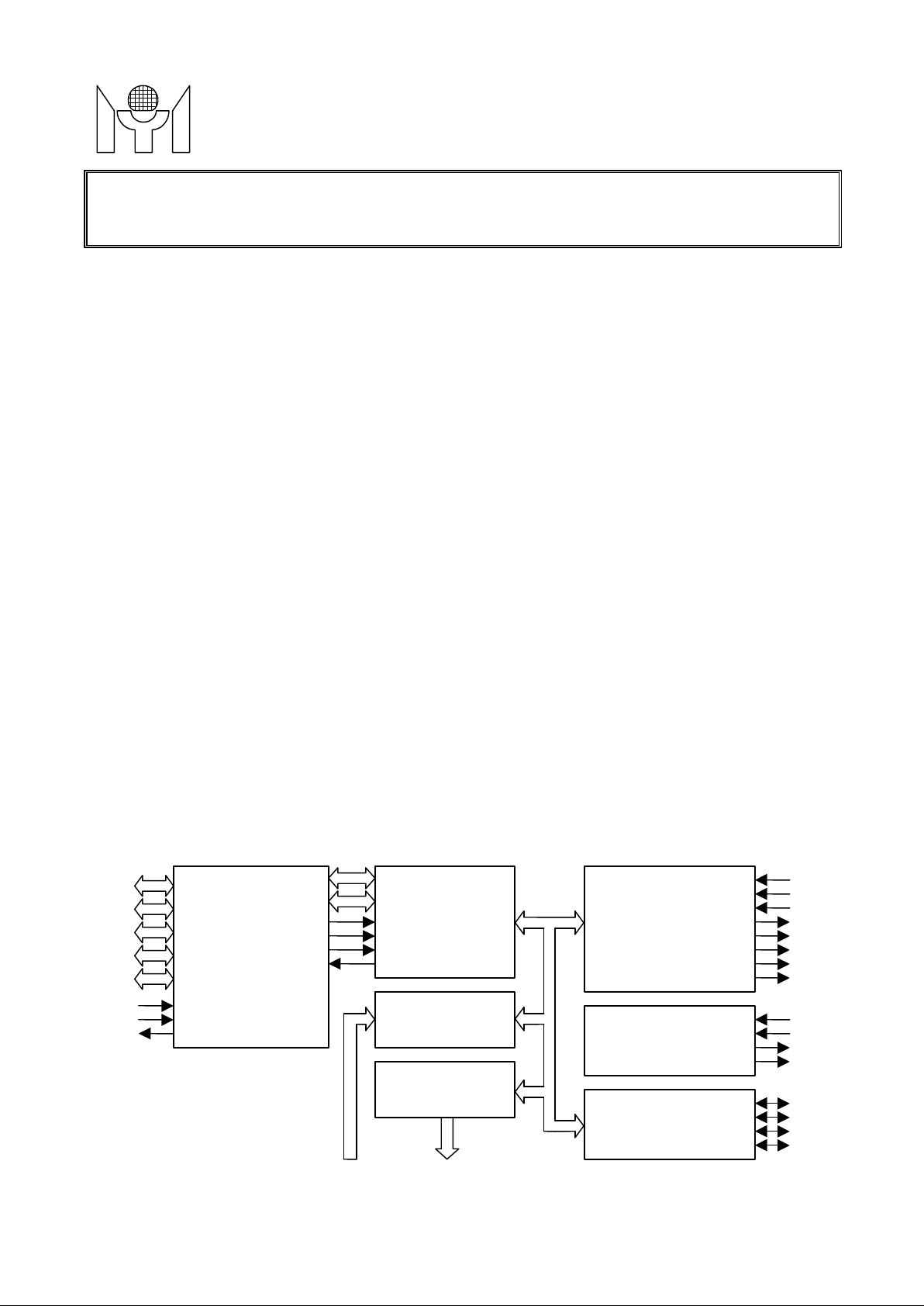
applications. It includes an 8051 CPU core, 1024-byte SRAM, OSD controller, 4 built-in PWM DACs, VESA
DDC interface, 4-channel A/D converter, a 64K-byte internal program Flash-ROM an d a 9K-word internal
CONTROL
INTERFACE
AD0-3
DA0-3
P0.0-7
P2.0-3
P0.0-7
P2.0-3
P1.0-7
P3.0-2
P3.4-5
P4.0-7
P5.0-7
CONTROL
MTV230M
TECHNOLOGY
(Rev 1.0)
8051 Embedded LCD Monitor Controller
with Flash OSD
FEATURES
• 8051 core, 12MHz operating frequency with double CPU clock option, 3.3V power supply.
•
• Maximum 4 channels of 5V open-drain PWM DAC.
• Maximum 32 bi-directional I/O pins.
• SYNC processor for composite separation/insertion, H/V polarity/frequency check and polarity adjustment.
• Built-in low power reset circuit.
• Compliant with VESA DDC2B/2Bi/2B+ standard.
• Dual slave IIC addresses.
• Single master IIC interface for internal device communication.
• Maximum 4-channel 6-bit ADC.
• Watchdog timer with programmable interval.
• OSD controller features:
. Full-screen display consists of 15 (rows) by 30 (columns) characters.
. Programmable OSD menu positioning for display screen center.
. 512 Flash-ROM fonts, with 12x18 dot matrix, including 480 standard fonts and 32 multi-color fonts.
.
. Character bordering, shadowing and blinking effect.
. Character height control (18 to 71 lines), double height and/or width control.
. 4 programmable windows with multi-level operation and programmable shadowing width/height/color.
•
• 42-pin SDIP or 44-pin PLCC/QFP package.
program Flash-ROM.
GENERAL DESCRIPTIONS
The MTV230M micro-controller is an 8051 CPU core embedded device specially tailored to LCD Monitor
OSD character Flash-ROM.
BL OCK DIAGRAM
OSDHS
OSDVS
XIN
ROUT
GOUT
BOUT
FBKG
INT
HSYNC
VSYNC
HBLANK
VBLANK
ISCL
ISDA
HSCL
HSDA
RST
X1
X2
8051
CORE
RD
WR
ALE
INT1
RD
WR
ALE
INT1
PWM DAC
XFR
ADC
OSD
H/VSYNC
DDC & IIC
This datasheet contains new product information. Myson Technology reserves the rights to modify the product specification without
notice. No liability is assumed as a result of the use of this product. No rights under any patent accompany the sale of the product.
Revision 1.0 - 1 - 2000/11/15
Page 2
MYSON
P6.1/ISDA
P1.0
P1.1
P6.0/ISCL
P1.2
P1.3
VDD
RST
VSS
P3.4/T0
P3.5/T1
P4.6/HBLANK
P4.7/VBLANK
OSDHS
XIN
ROUT
GOUT
BOUT
FBKG
INT/P6.2
P5.7/DA3
P4.1/VSYNC
OSDVS
PLCC
242322212028272625
6543214443424140
19
18
P4.1/VSYNC
P4.0/HSYNC
P3.1/Txd/HSDA
P3.2/INT0
VSS
OSDVS
P4.7/VBLANK
P4.6/HBLANK
P3.4/T0
MTV230M
TECHNOLOGY
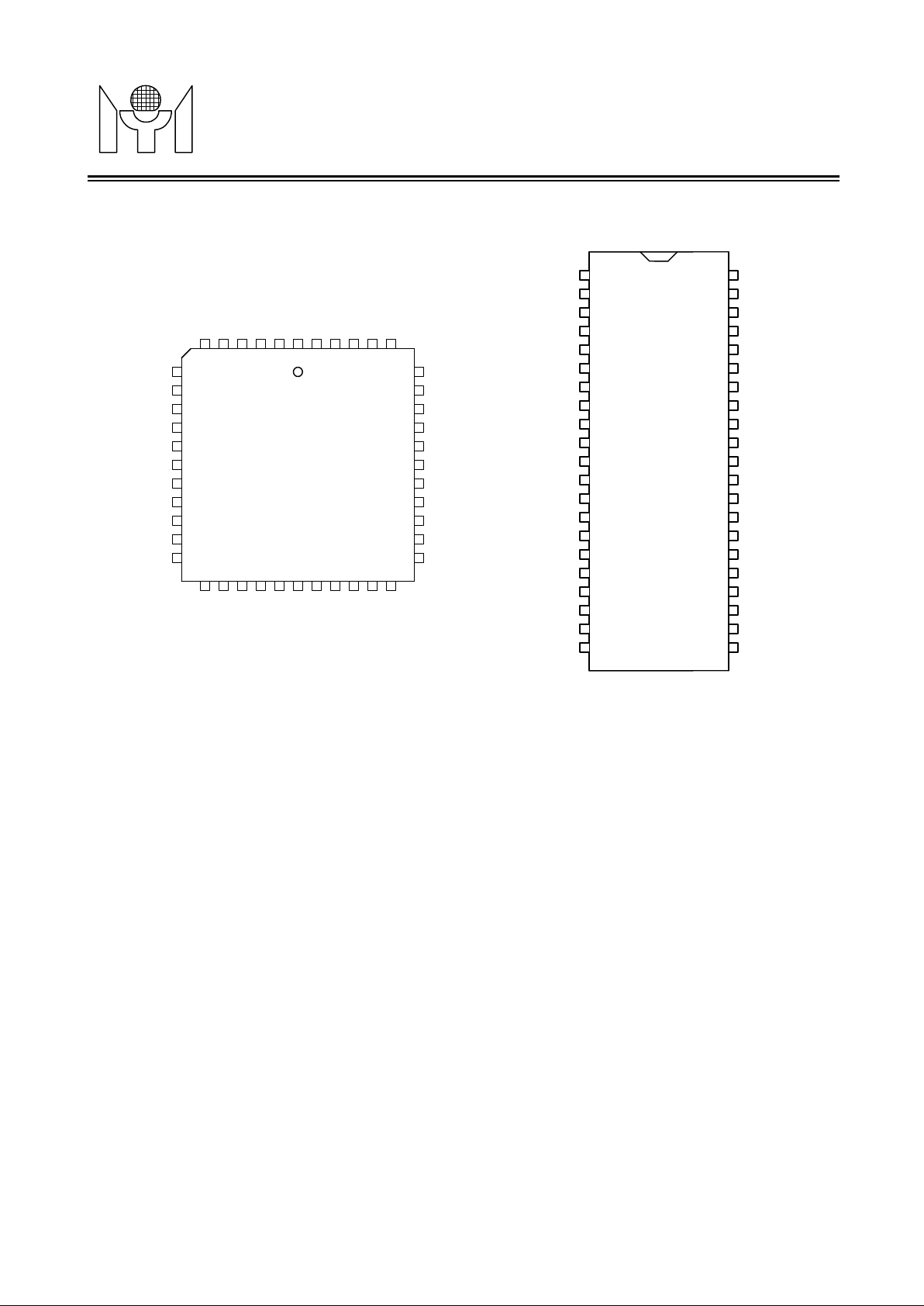
PIN CONNECTION
X1
7
X2
8
P4.5
9
P4.4
10
P4.3
11
P4.2
12
13
P4.0/HSYNC
P3.0/Rxd/HSCL
P3.1/Txd/HSDA
P3.2/INT0
14
15
16
17
MTV230M
44 Pin
39
38
37
36
35
34
33
32
31
30
29
P5.6/DA2
P5.5/DA1
P5.4/DA0
P5.3/AD3
P5.2/AD2
P5.1/AD1
P5.0/AD0
P1.7
P1.6
P1.5
P1.4
ROUT401
XIN
OSDHS
X1
X2
P4.5
P4.4
P4.3
P4.2
P3.0/Rxd/HSCL
VDD
RST
2
3
4
5
6
7
8
9
10
11
12
13
14
15
16
17
18
19
20
MTV230M
42 Pin
SDIP
(Rev 1.0)
GOUT
42
BOUT
41
FBKG
39
INT/P6.2
38
P5.7/DA3
37
P5.6/DA2
36
P5.5/DA1
35
P5.4/DA0
34
P5.1/AD1
33
P5.0/AD0
32
P1.7
31
P1.6
30
P1.5
29
P1.4
28
P1.3
27
P1.2
26
P1.1
25
P1.0
24
P6.1/ISDA
23
P6.0/ISCL
2221
P3.5/T1
Revision 1.0 - 2 - 2000/11/15
Page 3
MYSON
driving heavy load device.
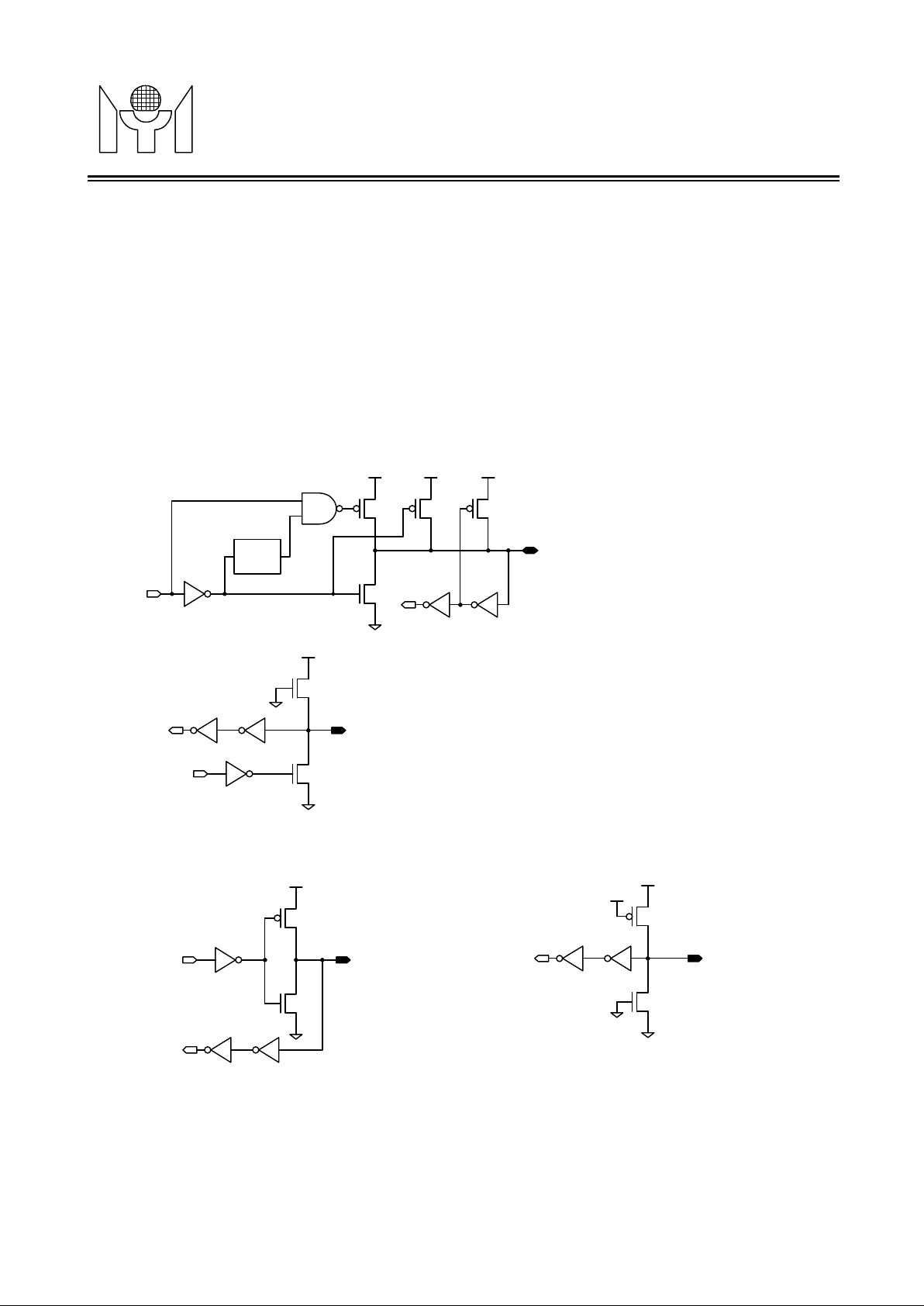
CMOS Pin (Output Mod e)
CMOS Pin (Input Mo d e)
MTV230M
TECHNOLOGY
(Rev 1.0)
PIN CONFIGURATION
A “CMOS pin” can be used as Input or Output mode. To use these pins as output mode, S/W needs to set
the corresponding output enable control bit “Pxxoe” to 1. Otherwise, the “Pxxoe” should clear to 0. In Output
mode, these pins can sink and drive at least 4mA current.
A “5V open drain pin” means it can sink at least 4mA current but no drive current to VDD. It can be used as
input or output function and needs an external pull up resistor.
A “8051 standard pin” is a pseudo open drain pin. It can sink at least 4mA current when output low level, and
drive at least 4mA current for 160nS when output transit from low to high, then keep drive 1 00uA to maintain
the pin at a high level. It can be used as input or output function. It needs an external pull up resistor when
Output
Data
2 OSC
period
delay
4mA 10uA
4mA
Input
Data
120uA
Pin
8051 Stand ard Pin
Input
Data
Output
Data
Output
Data
Input
Data
4mA
4mA
Pxxoe = 1
No Current
Pin
4mA
Pin
5V Open Drain Pin
Input
Data
No Current
Pin
No Current
Pxxoe = 0
Revision 1.0 - 3 - 2000/11/15
Page 4
MYSON
MTV230M
TECHNOLOGY
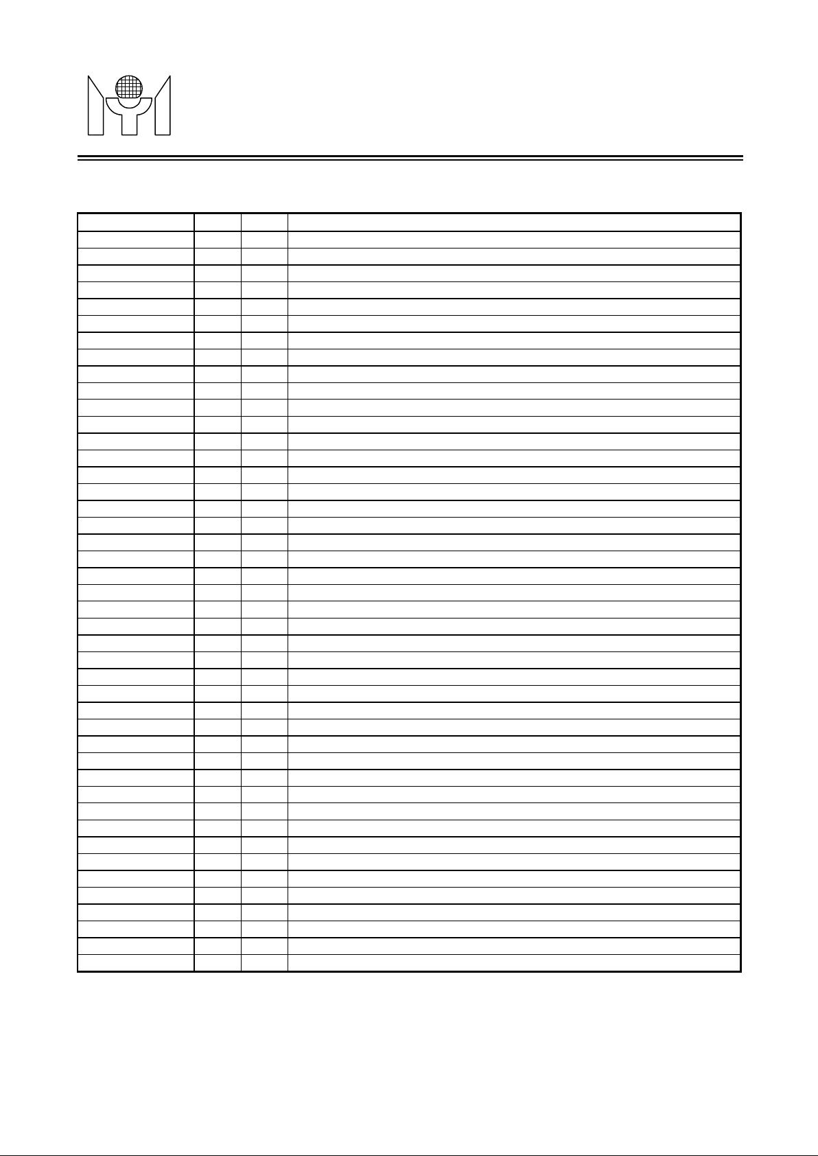
PIN DESCRIPTION
Name Type
RST
VDD
VSS
X2
X1
P1.0
P1.1
P1.2
P1.3
P1.4
P1.5
P1.6
P1.7
P3.0/Rxd /HSCL
P3.1/Txd/HSDA
P3.2/INT0
P3.4/T0
P3.5/T1
P4.7/VBLANK
P4.6/HBLANK
P4.5/HCLAM P
P4.4
P4.3
P4.2
P4.1/VSYNC
P4.0/HSYNC
P5.7/DA3
P5.6/DA2
P5.5/DA1
P5.4/DA0
P5.3/AD3
P5.2/AD2
P5.1/AD1
P5.0/AD0
P6.0/ISCL
P6.1/ISDA
INT/P6.2
FBKG
BOUT
GOUT
ROUT
XIN
OSDHS
OSDVS
O 8 Oscillator output
I/O 25 General purpose I/O (8051 standard)
I/O 26 General purpose I/O (8051 standard)
I/O 27 General purpose I/O (8051 standard)
I/O 28 General purpose I/O (8051 standard)
I/O 29 General purpose I/O (8051 standard)
I/O 30 General purpose I/O (8051 standard)
I/O 31 General purpose I/O (8051 standard)
I/O 32 General purpose I/O (8051 standard)
I/O 15 General purpose I/O / Rxd / Slave IIC clock (5V open drain)
I/O 16 General purpose I/O / Txd / Slave IIC data (5V open drain)
I/O 17 General purpose I/O / INT0 (8051 standard)
I/O 21 General purpose I/O / T0 (8051 standard)
I/O 22 General purpose I/O / T1 (8051 standard)
I/O 5 General purpose I/O / Vertical blank output (CMOS)
I/O 6 General purpose I/O / Horizontal blank output (CMOS)
I/O 9 General purpose I/O / Hclamp output (CMOS)
I/O 10 General purpose I/O (CMOS)
I/O 11 General purpose I/O (CMOS)
I/O 12 General purpose I/O (CMOS)
I/O 13 General purpose I/O / Vsync input (5V open drain)
I/O 14 General purpose I/O / Hsync or Xsync input (5V open drain)
I/O 40/38 General purpose I/O / PWM DAC output (5V open drain)
I/O 39/37 General purpose I/O / PWM DAC output (5V open drain)
I/O 38/36 General purpose I/O / PWM DAC output (5V open drain)
I/O 37/35 General purpose I/O / PWM DAC output (5V open drain)
I/O 36/- General purpose I/O / ADC Input (CMOS)
I/O 35/- General purpose I/O / ADC Input (CMOS)
I/O 34 General purpose I/O / ADC Input (CMOS)
I/O 33 General purpose I/O / ADC Input (CMOS)
I/O 23 General purpose output / Master IIC clock (5V open drain)
I/O 24 General purpose output / Master IIC data (5V open drain)
O 41/39 OSD intensity output / General purpose output (CMOS)
O 42/40 OSD fast blanking output (CMOS)
O 43/41 OSD blue color video signal output (CMOS)
O 44/42 OSD green color video signal output (CMOS)
O 1 OSD red color video signal output (CMOS)
#44/42
I 19 Active high reset
- 18 Positive Power Supply
- 20 Ground
I 7 Oscillator input
I 2 OSD pixel clock input (CMOS)
I 3 OSD vertical SYNC input (CMOS)
I 4 OSD horizontal SYNC input (CMOS)
Description
(Rev 1.0)
Revision 1.0 - 4 - 2000/11/15
Page 5
MYSON
FUNCTIONAL DESCRIPTIONS
fetches its program code from the 64K bytes Flash in MTV230M. It uses Port0 and Port2 to access the
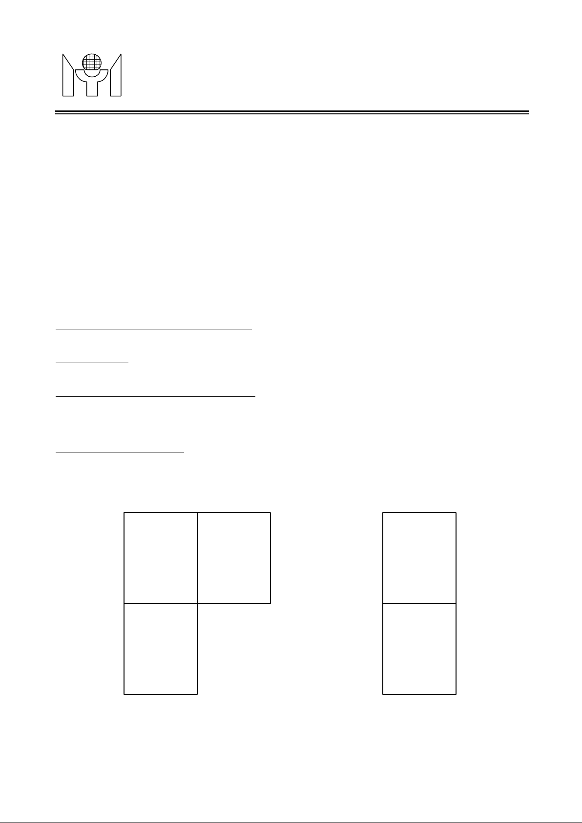
2. Memory Allo catio n
2.4 Auxiliary RAM (AUXRAM)
MTV230M
TECHNOLOGY
1. 8051 CPU Core
(Rev 1.0)
The CPU core of MTV230M is compatible with the industry standard 8051, which incl udes 256 bytes RAM,
Special Function Registers (SFR), two timers, five interrupt sources and serial interface. The CPU core
“external special function register” (XFR) and external auxiliary RAM (AUXRAM).
The CPU core can run at double rate when FclkE is set. Once the bit is set, the CPU runs as if a 24MHz X’tal
is applied on MTV230M, but the peripherals (IIC, DDC, H/V processor ) still run at the original frequency.
Note: All registers listed in this document reside in 8051’s external RAM area (XFR). For internal RAM
memory map, please refer to 8051 spec.
2.1 Internal Special Function Registers (SFR)
The SFR is a group of registers that are the same as standard 8051.
2.2 Internal RAM
There are total 256 bytes internal RAM in MTV230M, same as standard 8052.
2.3 External Special Function Registers (XFR)
The XFR is a group of registers allocated in the 8051 external RAM area F00h - FFFh. These registers are
used for OSD control or other special function. Program can use "MOVX" instruction to access these
registers.
There are total 768 bytes auxiliary RAM allocated in the 8051 external RAM area 800h - AFFh. Program can
use "MOVX" instruction to access the AUXRAM.
FFh
Internal RAM
Accessible by
addressing only
MOV A,@Ri
instruction)
80h
7Fh
Internal RAM
Accessible by
direct and indirect
addressing
indirect
(Using
SFR
Accessible by
direct addressing
FFFh
F00h
AFFh
XFR
Accessible by
indirect external
RAM addressing
(Using MOVX
instruction)
AUXRAM
Accessible by
indirect external
RAM addressing
(Using MOVX
instruction
00h
800h
Revision 1.0 - 5 - 2000/11/15
Page 6
MYSON
PWMF
MTV230M
TECHNOLOGY
3. Chip Configu ratio n
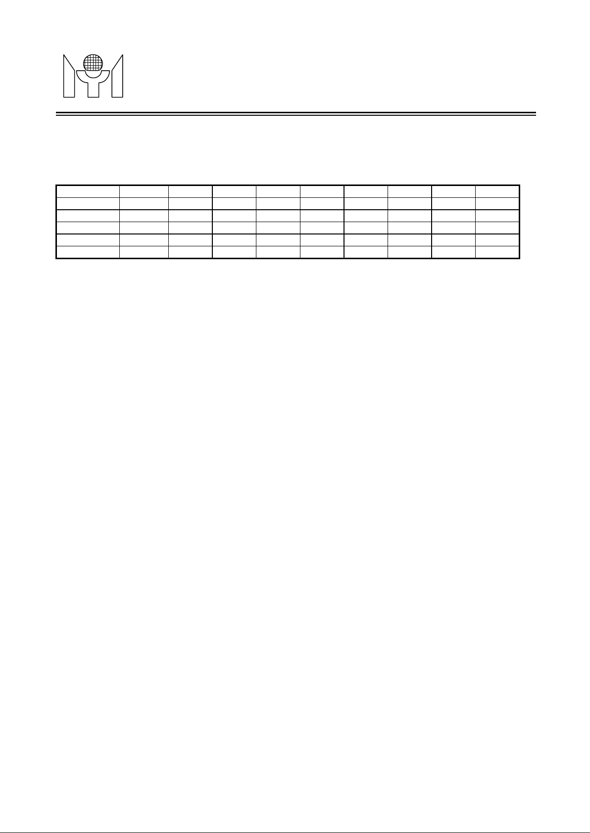
The Chip Configuration registers define the chip pins function, as well as the connection, configuration and
frequency of the functional block.
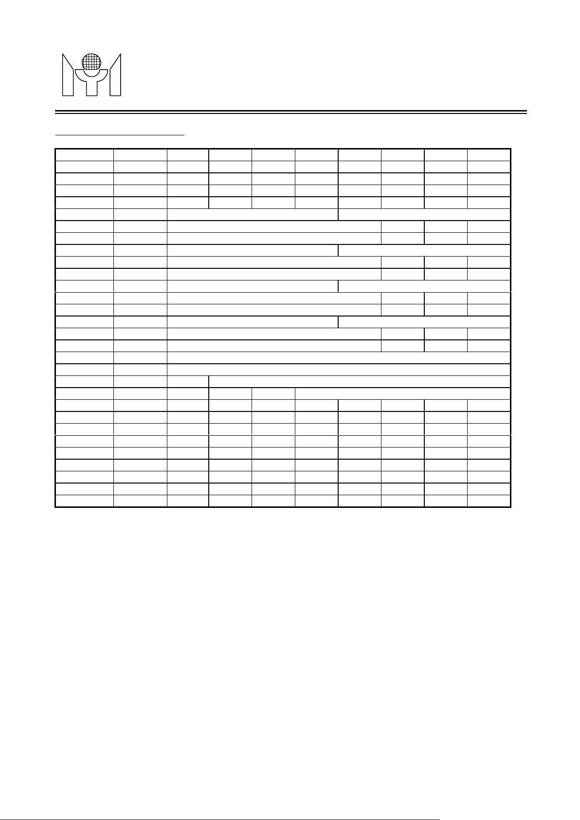
Reg name addr bi t7 bit6 bit5 Bit4 bit 3 b it2 bit1 bit0
PADMOD
PADMOD
PADMOD
PADMOD
OPTION
PADMOD (w) : Pad mode control registers. (All are "0" in Chip Reset)
HIICE = 1 → pin “P3.0/Rxd/HSCL” is HSCL; pin “P3.1/Txd/HSDA” is HSDA.
IIICE = 1 → pin “P6.1/ISDA” is ISDA; pin “P6.0/ISCL” is ISCL.
HVE = 1 → pin “P4.7/VBLANK” is VBLANK; pin “P4.6/HBLANK” is HBLANK.
HclpE = 1 → pin “P4.5/HCLAMP” is HCLAMP.
FclkE = 1 → CPU is running at double rate.
P62E = 1 → pin “INT/P6.2” is P6.2.
DA3E = 1 → pin “P5.7/DA3” is DA3.
DA2E = 1 → pin “P5.6/DA2” is DA2.
DA1E = 1 → pin “P5.5/DA1” is DA1.
DA0E = 1 → pin “P5.4/DA0” is DA0.
AD3E = 1 → pin “P5.3/AD3” is AD3.
AD2E = 1 → pin “P5.2/AD2” is AD2.
AD1E = 1 → pin “P5.1/AD1” is AD1.
AD0E = 1 → pin “P5.0/AD0” is AD0.
P47oe = 1 → P4.7 is output pin.
P46oe = 1 → P4.6 is output pin.
P45oe = 1 → P4.5 is output pin.
P44oe = 1 → P4.4 is output pin.
P43oe = 1 → P4.3 is output pin.
P42oe = 1 → P4.2 is output pin.
F2Bh (w) HIICE IIICE HVE HclpE FclkE P62E
F2Ch (w) DA3E DA2E DA1E DA0E AD3E AD2E AD1E AD0E
F2Dh (w) P47oe P46oe P45oe P44oe P43oe P42oe P41oe P40oe
F2Eh (w) P57oe P56oe P55oe P54oe P53oe P52oe P51oe P50oe
F2Fh (w)
= 0 → pin “P3.0/Rxd/HSCL” is P3.0/Rxd; pin “P3.1/Txd/HSDA” is P3.1/Txd.
= 0 → pin “P6.1/ISDA” is P6.1; pin “P6.0/ISCL” is P6.0.
= 0 → pin “P4.7/VBLANK” is P4.7; pin “P4.6/HBLANK” is P4.6.
= 0 → pin “P4.5/HCLAMP” is P4.5.
= 0 → CPU is running at normal rate.
= 0 → pin “INT/P6.2” is INT.
= 0 → pin “P5.7/DA3” is P5.7.
= 0 → pin “P5.6/DA2” is P5.6.
= 0 → pin “P5.5/DA1” is P5.5.
= 0 → pin “P5.4/DA0” is P5.4.
= 0 → pin “P5.3/AD3” is P5.3.
= 0 → pin “P5.2/AD2” is P5.2.
= 0 → pin “P5.1/AD1” is P5.1.
= 0 → pin “P5.0/AD0” is P5.0.
= 0 → P4.7 is input pin.
= 0 → P4.6 is input pin.
= 0 → P4.5 is input pin.
= 0 → P4.4 is input pin.
= 0 → P4.3 is input pin.
DIV253 SlvAbs1 SlvAbs0 ENSCL Msel MIICF1 MIICF0
(Rev 1.0)
Revision 1.0 - 6 - 2000/11/15
Page 7

MYSON
Selects 94KHz PWM frequency.
Selects 47KHz PWM frequency.
Selects 50KHz Master IIC frequency.
oe and P5(n)
MTV230M
TECHNOLOGY
= 0 → P4.2 is input pin.
P41oe = 1 → P4.1 is output pin.
= 0 → P4.1 is input pin.
P40oe = 1 → P4.0 is output pin.
= 0 → P4.0 is input pin.
P57oe = 1 → P5.7 is output pin.
= 0 → P5.7 is input pin.
P56oe = 1 → P5.6 is output pin.
= 0 → P5.6 is input pin.
P55oe = 1 → P5.5 is output pin.
= 0 → P5.5 is input pin.
P54oe = 1 → P5.4 is output pin.
= 0 → P5.4 is input pin.
P53oe = 1 → P5.3 is output pin.
= 0 → P5.3 is input pin.
P52oe = 1 → P5.2 is output pin.
= 0 → P5.2 is input pin.
P51oe = 1 → P5.1 is output pin.
= 0 → P5.1 is input pin.
P50oe = 1 → P5.0 is output pin.
= 0 → P5.0 is input pin.
(Rev 1.0)
OPTION (w) : Chip option configuration (All are "0" in Chip Reset).
PWMF = 1 →
= 0 →
DIV253 = 1 → PWM pulse width is 253 step resolution.
SlvAbs1,SlvAbs0 : Slave IIC block A's slave address length.
ENSCL = 1 → Enables slave IIC block to hold HSCL pin l ow while MTV230M is not able to
catch-up the speed of external master.
Msel = 1 → Master IIC block connects to HSCL/HSDA pins.
MIICF1,MIICF0 = 1,1 → Selects 400KHz Master IIC frequency.
4. I/O Ports
4.1 Port1
Port1 is a group of pseudo open drain pins. It can be use as general purpose I/O. The b ehavior Port is the
same as standard 8051.
= 0 → PWM pulse width is 256 step resolution.
= 1,0 → 5-bits slave address.
= 0,1 → 6-bits slave address.
= 0,0 → 7-bits slave address.
= 0 → Master IIC block connecst to ISCL/ISDA pins.
= 1,0 → Selects 200KHz Master IIC frequency.
= 0,1 →
= 0,0 → Selects 100KHz Master IIC frequency.
4.2 P3.0-2, P3.4-5
If these pins are not set as IIC pins, Port3 can be used as general purpose I/O, interrupt, UART and Timer
pins. The behavior of Port3 is the same as standard 8051.
4.3 Port4, Port5 and Port6
Port4 and Port5 are used as general purpose I/O. S/W needs to set the corresponding P4(n)
Revision 1.0 - 7 - 2000/11/15
oe
Page 8
MYSON
to define whether these pins are input or output. Port6 is purely output.
Each PWM DAC output pulse width of the converter is controlled by an 8-bit register in XFR. The frequency
of PWM clock is 47KHz or 94KHz, selected by PWMF. And the total duty cycle step of these DAC outputs is
Pulse width of PWM DAC 0
Pulse width of PWM DAC 1
Pulse width of PWM DAC 2
Pulse width of PWM DAC 3
* All of PWM DAC converters are centered with value 80h after power on.
MTV230M
TECHNOLOGY
Reg name addr bi t7 bit6 bit5 b it4 bit3 bit 2 bi t1 bit0
PORT4
PORT4
PORT4
PORT4
PORT4
PORT4
PORT4
PORT4
PORT5
PORT5
PORT5
PORT5
PORT5
PORT5
PORT5
PORT5
PORT6
PORT6
PORT6
F30h(r/w) P40
F31h(r/w) P41
F32h(r/w) P42
F33h(r/w) P43
F34h(r/w) P44
F35h(r/w) P45
F36h(r/w) P46
F37h(r/w) P47
F38h(r/w) P50
F39h(r/w) P51
F3Ah(r/w) P52
F3Bh(r/w) P53
F3Ch(r/w) P54
F3Dh(r/w) P55
F3Eh(r/w) P56
F3Fh(r/w) P57
F28h(w) P60
F29h(w) P61
F2Ah(w) P62
(Rev 1.0)
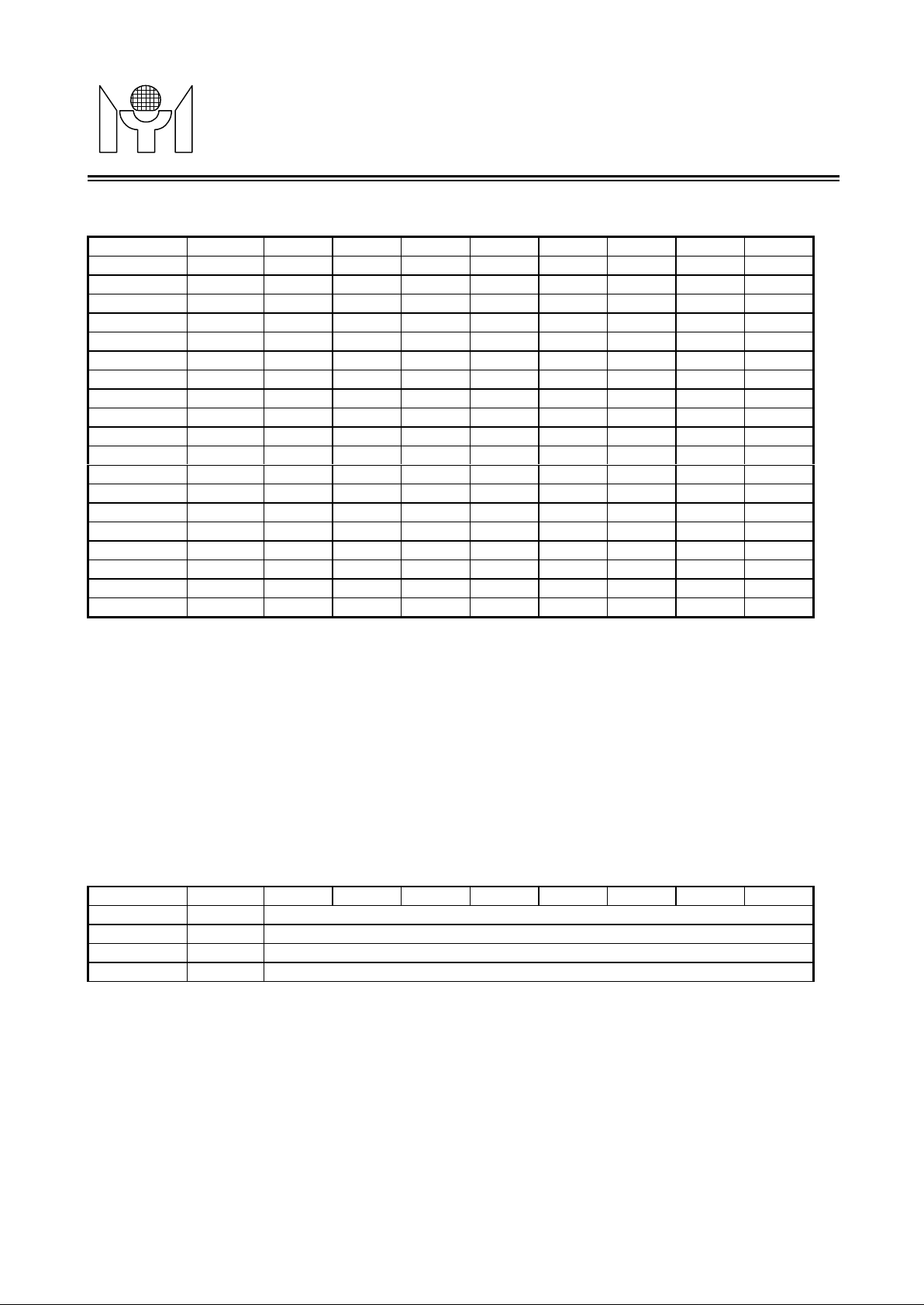
PORT4 (r/w) : Port 4 data input/output value.
PORT5 (r/w) : Port 5 data input/output value.
PORT6 (w) : Port 6 data output value.
5. PWM DAC
253 or 256, selected by DIV253. If DIV253=1, writing FDH/FEH/FFH to DAC reg ister ge nerates stable high
output. If DIV253=0, the output will pulse low at least once even if content of the DAC reg ister is FFH. Writing
00H to DAC register generates stable low output.
Reg name addr bi t7 bit6 bit5 b it4 bit3 bit 2 bi t1 bit0
DA0
DA1
DA2
DA3
DA0-3 (r/w) : The output pulse width control for DA0-3.
F20h (r/w)
F21h (r/w)
F22h (r/w)
F23h (r/w)
Revision 1.0 - 8 - 2000/11/15
Page 9
MYSON
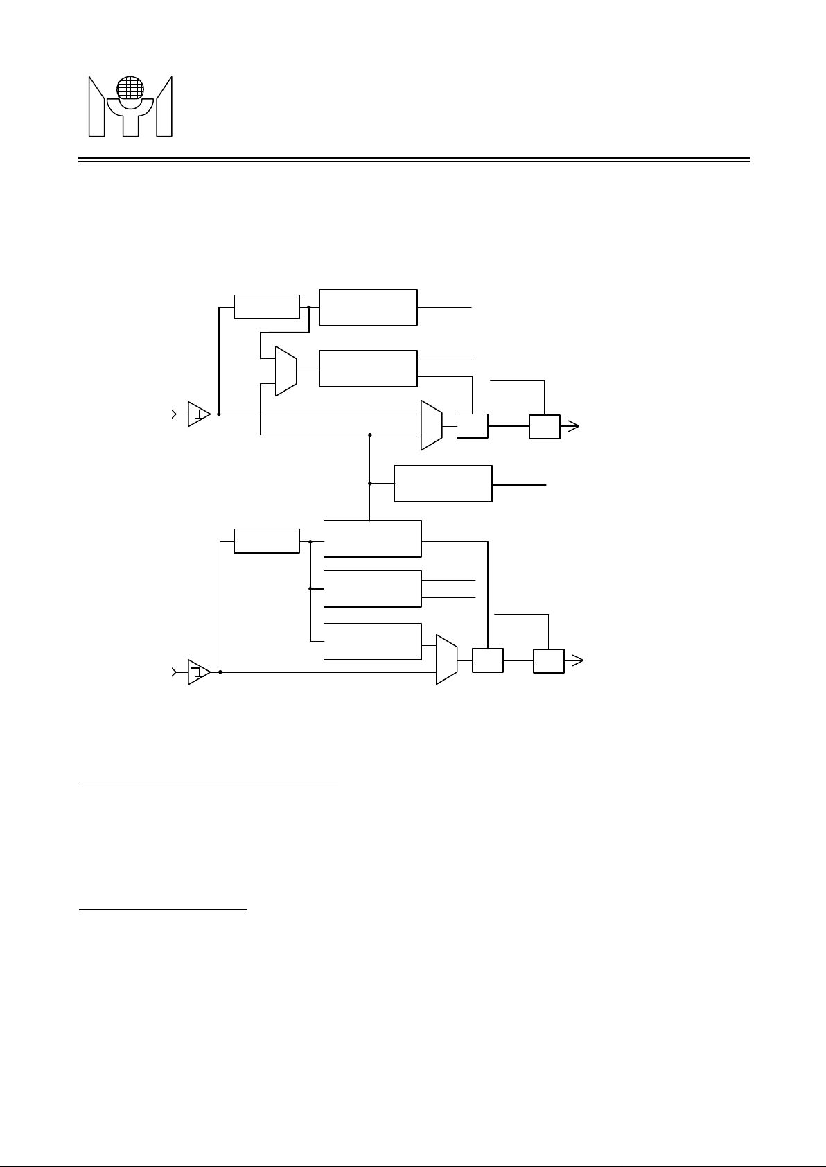
inputs presence check, frequency counting, polarity detection and H/V output polarity control. The present
CVpre flag is set and users can select the extracted "CVSYNC" for the source of polarity check,
6.2 H/V Frequency Counter
VSYNC/CVSYNC is present or continuously updated when VSYNC/CVS YNC is non-present. The 12 bits
Hpol
CVpre
Vbpl
VSYNC
Vpre
Vfreq
Vpol
VBLANK
HSYNC
CVSYNC
Hpre
Hfreq
Hbpl
HBLANK
XOR
MTV230M
TECHNOLOGY
(Rev 1.0)
6. H/V SYNC Processing
The H/V SYNC processing block performs the functions of composite signal separation /insertion, SYNC
and frequency function block treat any pulse shorter than one OSC period as noise.
Digital Filter
Present
Check
Polarity Check &
Freq. Count
Present
Check
XOR
XOR
Digital Filter
Polarity Check &
Sync Seperator
Present Check &
Freq. Count
Composite
Pulse Insert
XOR
H/V SYNC Processor Block Diagram
6.1 Composite SYNC Separation/Insertion
The MTV230M continuously monitors the input HSYNC, if the vertical SYNC pulse can be extracted from the
input, a
frequency count, and VBLANK output. The CVSYNC will have 8us delay compared to the original signal.
The MTV230M can also insert pulse to HBLANK output during com posite active time of VSYNC. The width
of the insert pulse is 1/8 HSYNC period and the insertion frequency can adapt to original HSYNC. The insert
pulse of HBLANK can be disabled or enabled by setting “NoHins” control bit.
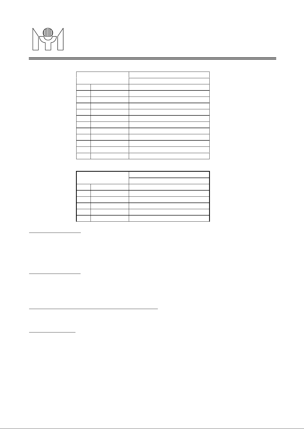
MTV230M can discriminate HSYNC/VSYNC frequency and saves the information in XFRs. The 14 bits
Hcounter counts the time of 64xHSYNC period, then loads the result into the HCNTH/HCNTL latch. The
output value will be [(128000000/H-Freq) - 1], updated once per VSYNC/CVSYNC perio d when
Vcounter counts the time between two VSYNC pulses, then loads the result into the VCNTH/VCNTL latch.
The output value will be (62500/V-Freq), updated every VSYNC/CVSYNC perio d. An extra overflow bit
indicates the condition of H/V counter overflow. The VFchg/HFchg interrupt is set when VCNT/HCNT value
changes or overflowes. Table 6.2.1 and table 6.2.2 show the HCNT/VCNT value under the operations of
12MHz.
Revision 1.0 - 9 - 2000/11/15
Page 10
MYSON
CVpre flag interrupt may be disabled when S/W disables the composite function.
6.4 H/V Polarity Detect
The polarity functions detect the input HSYNC/VSYNC high and low pulse duty cycle. If the high pulse
duration is longer than that of the low pulse, the negative polarity is asserted; otherwise, positive polarity is
6.5 Output HBLANK/VBLANK Control and Polarity Adjust
mux selection and output polarity are S/W controllable.
flag is set each time when MTV230M detects a VSYNC pulse. The flag is cleared by S /W writing a "0".
MTV230M
TECHNOLOGY
6.2.1 H-Freq Table
H-Freq(KHZ)
1
2
3
4
5
6
7
8
9
10
11
12
6.2.2 V-Freq Table
1
2
3
4
5
6
31.5
37.5
43.3
46.9
53.7
60.0
68.7
75.0
80.0
85.9
93.8
106.3
V-Freq(Hz)
56
60
70
72
75
85
Outpu t Value (14 bit s )
12MHz OSC (hex / dec)
Outpu t value (12bits)
12MHz OSC (hex / dec)
(Rev 1.0)
0FDEh / 4062
0D54h / 3412
0B8Bh / 2955
0AA8h / 2728
094Fh / 2383
0854h / 2132
0746h / 1862
06AAh / 1706
063Fh / 1599
05D1h / 1489
0554h / 1364
04B3h / 1203
45Ch / 1116
411h / 1041
37Ch / 892
364h / 868
341h / 833
2DFh / 735
6.3 H/V Present Check
The Hpresent function checks the input HSYNC pulse, Hpre flag is set when HSYNC is over 10KHz or
cleared when HSYNC is under 10Hz. The Vpresent function checks the input VSYNC pulse, the Vpre flag is
set when VSYNC is over 40Hz or cleared when VSYNC is under 10Hz. The HPRchg interrupt is set when
the Hpre value changes. The VPRchg interrupt is set when the Vpre/CVpre value changes. However, the
asserted. The HPLchg interrupt is set when the Hpol value changes. The VPLchg interrupt is set when the
Vpol value changes.
The HBLANK is the mux output of HSYNC and composite Hpulse. The VBLANK is the mux output of
VSYNC and CVSYNC. The
6.6 VSYNC Interrupt
The MTV230M checks the VSYNC input pulse and generates an interrupt at its leading edge. The VSYNC
Revision 1.0 - 10 - 2000/11/15
Page 11
MYSON
EVsync
The status of polarity, present and static level for HSYNC and VSYNC.
HSYNC input is positive polarity.
VSYNC (CVSYNC) is negative polarity.
Freq counter is overflowed, this bit is cleared by H/W when condition removed.
byteV-Freq counter.
Selects CVSYNC as the polarity,
Selects VSYNC as the polarity,
Negative polarity HBLANK output.
Positive polarity HBLANK output.
Negative polarity VBLANK output.
MTV230M
TECHNOLOGY
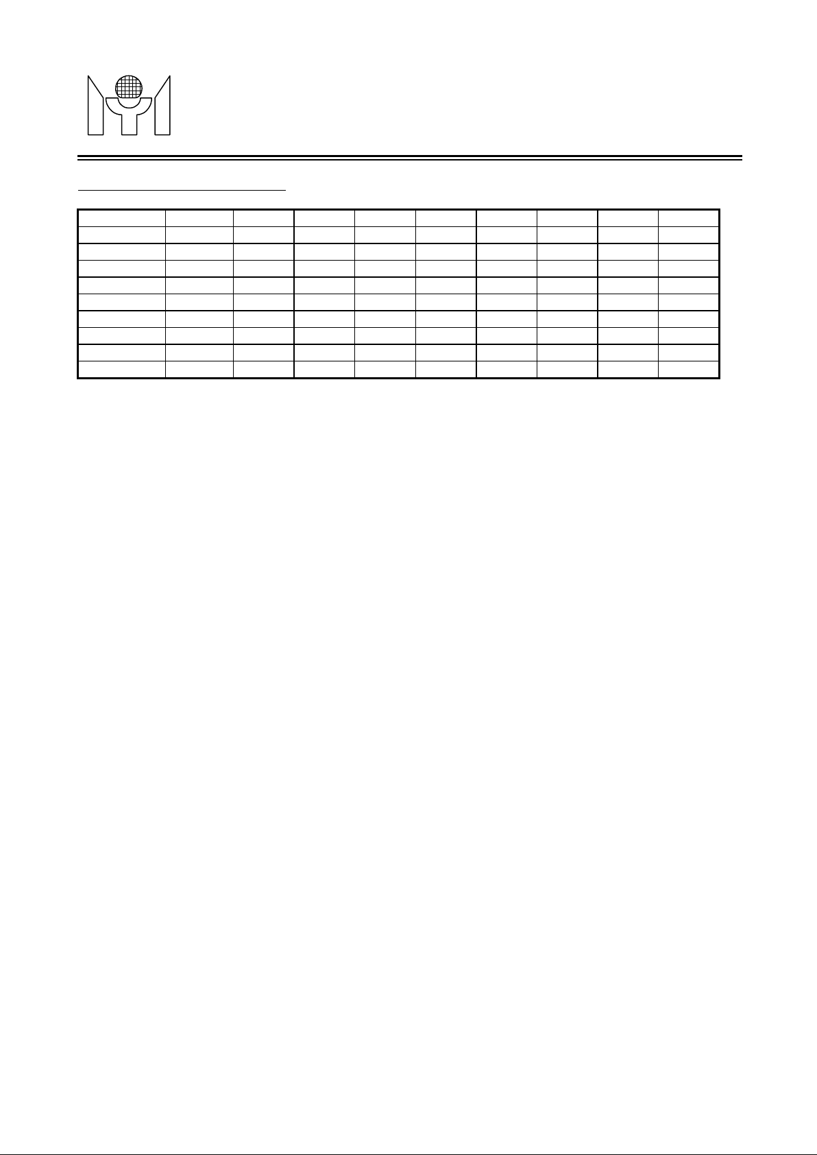
6.7 H/V SYNC Processor Register
Reg name addr bi t7 bit6 bit5 b it4 bit3 bit 2 bi t1 bit0
HVSTUS
HCNTH
HCNTL
VCNTH
VCNTL
HVCTR0
HVCTR3
INTFLG
INTEN
HVSTUS (r) :
CVpre = 1 → The extracted CVSYNC is present.
H
V
H
V
H
V
*H
F40h (r) CVpre Hpol Vpol Hpre Vpre Hoff Voff
F41h (r) Hovf HF13 HF12 HF11 HF10 HF9 HF8
F42h (r) HF7 HF6 HF5 HF4 HF3 HF2 HF1 HF0
F43h (r) Vovf VF11 VF10 VF9 VF8
F44h (r) VF7 VF6 VF5 VF4 VF3 VF2 VF1 VF0
F40h (w) C1 C0 NoHins HBpl VBpl
F43h (w) CLPEG CLPPO CLPW2 CLPW1 CLPW0
F48h (r/w) HPRchg VPRchg HPLchg VPLchg HFchg VFchg Vsync
F49h (w) EHPR EVPR EHPL EVPL EHF EVF
= 0 → The extracted CVSYNC is not present.
= 1 →
pol
= 0 → HSYNC input is negative polarity.
= 1 → VSYNC (CVSYNC) is positive polarity.
pol
= 0 →
= 1 → HSYNC input is present.
pre
pre
off*
off*
off
and V
= 0 → HSYNC input is not present.
= 1 → VSYNC input is present.
= 0 → VSYNC input is not present.
= 1 → The off level HSYNC input is high.
= 0 → The off level HSYNC input is low.
= 1 → The off level VSYNC input is high.
= 0 → The off level VSYNC input is low.
are valid when H
off
pre=0
or V
pre=0.
(Rev 1.0)
HCNTH (r) : High bits of H-Freq counter.
Hovf = 1 → H-Freq counter is overflowed, this bit is cleared b y H/W when condition removed.
HF13 - HF8 : 6 high bits of H-Freq cou nter.
HCNTL (r) : Low byte of H-Freq counter.
VCNTH (r) : High bits V-Freq of counter.
Vovf = 1 → VVF11 - 8 : 4 high bits of V-Freq counter.
VCNTL (r) : Low
HVCTR0 (w) : H/V SYNC processor control register 0.
C1, C0 = 1,1 →
NoHins = 1 → HBLANK has no insert pulse in composite mode.
HB
VB
Revision 1.0 - 11 - 2000/11/15
= 1,0 →
= 0,0 → Disables composite function.
= 0,1 → H/W auto switches to CVSYNC when CVpre=1 and VSpre=0.
= 0 → HBLANK has insert pulse in composite mode.
= 1 →
pl
= 0 →
= 1 →
pl
freq and VBLANK source.
freq and VBLANK source.
Page 12

MYSON
Positive polarity VBLANK output.
Positive polarity clamp pulse output.
Negative polarity clamp pulse output.
: CLPW0 : Pulse width of clamp pulse is
:CLPW0) + 1] x 0.167
enable bit is set, INT1 source of the 8051 core will be driven by a zero level. Software MUST
Clears HSYNC polarity change flag.
Clears VSYNC frequency change flag.
Indicates a HSYNC polarity change.
Enables HSYNC polarity change interrupt.
Enables VSYNC polarity change interrupt.
MTV230M
TECHNOLOGY
= 0 →
HVCTR3 (w) : HSYNC clamp pulse control register.
CLPEG = 1 → Clamp pulse follows HSYNC leading edge.
CLPPO = 1 →
INTFLG (w) : Interrupt flag. An interrupt event will set its individual flag, and, if the corresponding interrupt
HPRchg= 1 → No action.
VPRchg= 1 → No action.
HPLchg= 1 → No action.
VPLchg= 1 → No action.
HFchg = 1 → No action.
VFchg = 1 → No action.
Vsync = 1 → No action.
= 0 → Clamp pulse follows HSYNC trailing edge.
= 0 →
[(CLPW2
clear this register while serve the interrupt routine.
= 0 → Clears HSYNC presence change flag.
= 0 → Clears VSYNC presence change flag.
= 0 →
= 0 → Clears VSYNC polarity change flag.
= 0 → Clears HSYNC frequency change flag.
= 0 →
= 0 → Clears VSYNC interrupt flag.
CLPW2
µs for 12MHz X’tal selection.
(Rev 1.0)
INTFLG (r) : Interrupt flag.
HPRchg= 1 → Indicates a HSYNC presence change.
VPRchg= 1 → Indicates a VSYNC presence change.
HPLchg= 1 →
VPLchg= 1 → Indicates a VSYNC polarity change.
HFchg = 1 → Indicates a HSYNC f requency change or counter overflow.
VFchg = 1 → Indicates a VSYNC frequency change or counter overflow.
Vsync = 1 → Indicates a VSYNC interrupt.
INTEN (w) : Interrupt enable.
EHPR = 1 → Enables HSYNC presence change interrupt.
EVPR = 1 → Enables VSYNC presence change interrupt.
EHPL = 1 →
EVPL = 1 →
EHF = 1 → Enables HSYNC frequency change / counter overflow interrupt.
EVF = 1 → Enables VSYNC frequency change / counter overflow interrupt.
EVsync = 1 → Enables VSYNC interrupt.
7. DDC & IIC Int er face
7.1 DDC2B Mode
To perform DDC2 function, S/W can configure the Slave A IIC block to act as EEPROM behavior. The slave
address of the Slave A block can be chosen by S/W as 5-bits, 6-bits or 7-bits. For example, if S/W chooses
5-bits slave address as 10100b, the slave IIC block A will respond to slave address 10100xx b and save the 2
Revision 1.0 - 12 - 2000/11/15
Page 13

MYSON
written to RCABUF/RCBBUF register when a data byte is received. The first b yte loaded is word address
(slave address is dropped). This block also generates a RCAI/RCBI (receives buffer full interrupt) every time
WadrB flag can tell S/W that if the
SlvBMI is cleared by writing "0" to corresponding bit in INTFLG register.
The TXAI/TXBI is cleared by writing TXABUF/TXBBUF. If the control
The master mode IIC block can be connected to the ISDA /ISCL pins or the HSDA/HSCL pins, selected by
Msel control bit. Its speed can be selected to 50KHz-400KHz by S/W setting the MIICF1/MIICF0 control bit.
1. Write MBUF the Slave Address.
3. After the MTV230M transmit this byte, a
1. Write MBUF the Slave Address.
3. After the MTV230M transmit this byte, a
MTV230M
TECHNOLOGY
LSB "xx" in XFR. This feature enables MTV230M to meet PC99 requirement.
7.2 Slave Mode IIC Function Block
The slave mode IIC block is connected to HSDA and HSCL pins. This block can receive/transmit data using
IIC protocol. There are 2 slave addresses MTV230M can respond to. S/W may write the
SLVAADR/SLVBADR register to determine the slave addresses. The SlaveA address can be configured to
5-bits, 6-bits or 7-bits by S/W setting the SlvAbs1 and SlvAbs0 control bits.
In receive mode, the block first detects IIC slave address matching the condition then issues a
SlvAMI/SlvBMI interrupt. If the matched address is slave A, MTV230M will save the 2 LSB bits of the
matched address to SlvAlsb1 and SlvAlsb0 register. The data from HSDA is shifted into shift register then
the RCABUF/RCBBUF is loaded. If S/W is not able to read out the RCABUF/RC BBUF in time, the next byte
in shift register will not be written to RCABUF/RCBBUF and the slave block returns NACK to the master.
This feature guarantees the data integrity of communication. The WadrA/
data in RCABUF/RCBBUF is a word address.
In transmit mode, the block first detects IIC slave address match condition then issues a SlvAMI/SlvBMI
interrupt. In the mean time, the SlvAlsb1/SlvAlsb0 is also updated if the matched address is sla ve A, and the
data pre-stored in the TXABUF/TXBBUF is loaded into shift register, result in TXABUF/T XBBUF empty and
generates a TXAI/TXBI (transmit buffer empty interrupt). S/W should write the TXABUF/TXBBUF a new byte
for next transfer before shift register empties. A failure of this process will cause data corrupt. The TXAI/TXBI
occurs every time when shift register reads out the data from TXABUF/TXBBUF.
The SlvAMI/
cleared by reading RCABUF/RCBBUF.
bit ENSCL is set, the block will hold HSCL low until the RCAI/RCBI/TXAI/TXBI is cleared.
The RCAI/RCBI is
(Rev 1.0)
*Please see the attachments about "Slave IIC Block Timing".
7.3 Master Mode IIC Function Block
The software program can access the external IIC device through this interface. A summary of master IIC
access is illustrated as follows.
7.3.1. To write IIC Device
2. Set S bit to Start.
4. Program can write MBUF to transfer next byte or set P bit to stop.
* Please see the attachments about "Master IIC Transmit Timing".
7.3.2. To read IIC Device
2. Set S bit to Start.
4. Set or reset the MAckO flag according to the IIC protocol.
5. Read out MBUF the useless byte to continue the data transfer.
6. After the MTV230M receives a new byte, the MbufI interrupt is triggered again.
7. Read MBUF also trigger the next receive operation, but set P bit before read can terminate the operation.
* Please see the attachments about "Master IIC Receive Timing".
MbufI interrupt will be triggered.
MbufI interrupt will be triggered.
Revision 1.0 - 13 - 2000/11/15
Page 14
MYSON
WadrB
WadrA
SLVAADR
SLVBADR
In master receive mode, NACK is returned by MTV230M.
In master receive mode, ACK is returned by MTV230M.
enable bit is set, the 8051 INT1 source will be driven by a zero level. Software MUST clear
Indicates the RCBBUF has received a new data byte, cleared by reading
Indicates the RCABUF has received a new data byte, cleared by reading
MTV230M
TECHNOLOGY
Reg name addr bi t7 bit6 bit5 b it4 bit3 bit 2 bi t1 bit0
IICCTR
IICSTUS
IICSTUS
INTFLG
INTFLG
INTEN
MBUF
RCABUF
TXABUF
RCBBUF
TXBBUF
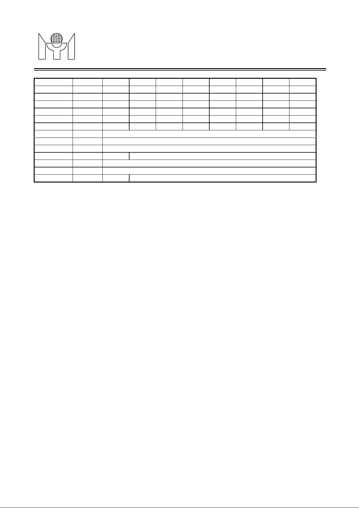
IICCTR (r/w) : IIC interface control register.
F00h (r/w) MAckO P S
F01h (r)
F02h (r) MAckIn
F03h (r) TXBI RCBI SlvBMI TXAI RCAI SlvAMI MbufI
F03h (w) SlvBMI SlvAMI MbufI
F04h (w) ETXBI ERCBI ESlvBMI ETXAI ERCAI ESlvAMI EMbufI
F05h (r/w) Master IIC receive/transmit data buffer
F06h (r) Slave A IIC receive buffer
F06h (w) Slave A IIC transmit buffer
F07h (w) ENSlvA Slave A IIC address
F08h (r) Slave B IIC receive buffer
F08h (w) Slave B IIC transmit buffer
F09h (w) ENSlvB Slave B IIC address
MAckO = 1 →
= 0 →
S, P = ↑, 0 → Start condition when Master IIC is not during transfer.
= X, ↑ → Stop condition when Master IIC is not during transfer.
= 1, X → Will resume transfer after a read/write MBUF operation.
SlvRWB SAckIn SLVS SlvAlsb1 SlvAlsb0
(Rev 1.0)
IICSTUS (r) : IIC interface status register.
WadrB = 1 → The data in RCBBUF is word address.
WadrA = 1 → The data in RCABUF is word address.
SlvRWB = 1 → Current transfer is slave transmit.
= 0 → Current transfer is slave receive.
SAckIn = 1 → The external IIC host respond NACK.
SLVS = 1 → The slave block has detected a START, cleared when STOP detected.
SlvAlsb1,SlvAlsb0 : The 2 LSB which host send to Slave A block.
MAckIn = 1 → Master IIC bus error, no ACK received from the slave IIC device.
= 0 → ACK received from the slave IIC device.
INTFLG (w) : Interrupt flag. A interrupt event will set its individual flag, and, if the corresponding interrupt
this register while serve the interrupt routine.
SlvBMI = 1 → No action.
= 0 → Clears SlvBMI flag.
SlvAMI = 1 → No action.
= 0 → Clears SlvAMI flag.
MbufI = 1 → No action.
= 0 → Clears Master IIC bus interrupt flag (MbufI).
INTFLG (r) : Interrupt flag.
TXBI = 1 → Indicates the TXBBUF needs a new data byte, cleared by writing TXBBUF.
RCBI = 1 →
RCBBUF.
SlvBMI = 1 → Indicates the slave IIC address B matches condition.
TXAI = 1 → Indicates the TXABUF needs a new data byte, cleared by writing TXABUF.
RCAI = 1 →
SlvAMI = 1 → Indicates the slave IIC address A match condition.
RCABUF.
Revision 1.0 - 14 - 2000/11/15
Page 15

MYSON
When the voltage level of power supply is below 2.7V for a specific period of time, the LVR will generate a
The Watchdog Timer automatically generates a device reset when it is overflowed. The interval of overflow is
WDT(2:0). The timer
9. A/D con v ert er
MTV230M
TECHNOLOGY
MbufI = 1 → Indicates a byte is sent/received to/from the master IIC bus.
INTEN (w) : Interrupt enable.
ETXBI = 1 → Enables TXBBUF interrupt.
ERCBI = 1 → Enables RCBBUF interrupt.
ESlvBMI = 1 → Enables slave address B match interrupt.
ETXAI = 1 → Enables TXABUF interrupt.
ERCAI = 1 → Enables RCABUF interrupt.
ESlvAMI = 1 → Enables slave address A match interrupt.
EMbufI = 1 → Enables Master IIC bus interrupt.
Mbuf (w) : Master IIC data shift register, after START and before STOP condition, writing this register
will resume transmission of MTV230M to the IIC bus.
Mbuf (r) : Master IIC data shift register, after START and before STOP condition, reading this register
will resume receiving of MTV230M from the IIC bus.
RCABUF (r) : Slave IIC block A receives d ata buffer.
TXABUF (w) : Slave IIC block A transmits data buffer.
(Rev 1.0)
SLVAADR (w) :Slave IIC block A's enable and address.
ENslvA = 1 → Enables slave IIC block A.
= 0 → Disables slave IIC block A.
bit6-0 : Slave IIC address A to which the slave block should respond.
RCBBUF (r) : Slave IIC block B receives d ata buffer.
TXBBUF (w) : Slave IIC block B transmits data buffer.
SLVBADR (w) :Enable and address of Slave IIC block B.
ENslvB = 1 → Enables slave IIC block B.
= 0 → Disables slave IIC block B.
bit6-0 : Slave IIC address B to which the slave block should respond.
8. Low Pow er Reset (LVR) & Watchdog Tim er
chip reset signal. After the power supply is above 2.7V, LVR maintain in reset state for 144 Xtal cycle to
guarantee the chip exit reset condition with a stable X'tal oscillation.
0.25 sec x N, where N is a number from 1 to 8, and can be programmed via register
function is disabled after power on reset, users can activate this function by setting WEN, and clear the timer
by set WCLR.
The MTV230M is equipped with four 6-bit A/D converters. S/W can select the current convert channel by
setting the SADC1/SADC0 bit. The refresh rate for the ADC is OSC freq./12288. The ADC compares the
input pin voltage with internal VDD*N/64 voltage (where N = 0 - 63). The ADC output va lue is N when pin
voltage is greater than VDD*N/64 and smaller than VDD*(N+1)/64.
Revision 1.0 - 15 - 2000/11/15
Page 16

MYSON
WCLR
WDT2
WDT1
WDT0
Watchdog Timer control register.
Enables Watchdog Timer.
Clears Watchdog Timer.
Whole Flash erase (Blank): 10mS
When ISP is enabled, the MTV230M will disable Watchdog reset and switch the Flash interface to ISP host
MTV230M
TECHNOLOGY
Reg name addr bi t7 bit6 bit5 b it4 bit3 bit 2 bi t1 bit0
ADC
ADC
WDT
WDT (w) :
WEN = 1 →
WCLR = 1 →
WDT2: WDT0 = 0 → Overflow interval = 8 x 0.25 sec.
ADC (w) : ADC control.
ENADC = 1 → Enables ADC.
SADC0 = 1 → Selects ADC0 pin input.
SADC1 = 1 → Selects ADC1 pin input.
SADC2 = 1 → Selects ADC2 pin input.
SADC3 = 1 → Selects ADC3 pin input.
F10h (w) ENADC SADC3 SADC2 SADC1 SADC0
F10h (r) ADC convert Result
F18h (w) W EN
= 1 → Overflow interval = 1 x 0.25 sec.
= 2 → Overflow interval = 2 x 0.25 sec.
= 3 → Overflow interval = 3 x 0.25 sec.
= 4 → Overflow interval = 4 x 0.25 sec.
= 5 → Overflow interval = 5 x 0.25 sec.
= 6 → Overflow interval = 6 x 0.25 sec.
= 7 → Overflow interval = 7 x 0.25 sec.
(Rev 1.0)
ADC (r) : ADC converts result.
10. In System Programm i n g fu n c ti o n (ISP)
The two Flash memories (OSD Flash and Code Flash) can be programmed by a specific WRITER in parallel
mode, or by IIC Host in serial mode while the system is working. The feature of ISP is outlined as below:
1. Single 3.3V power supply for Program/Erase/Verify.
2. Block Erase: 512 Byte for Program Code or 256 words f or OSD fonts, both are 10mS time.
3.
4. Byte/Word programming Cycle time: 60uS per byte, 120uS per word
5. Read access time: 40ns
6. Only one two-pin IIC bus (shared with DDC2) is needed for ISP in user/factory mode.
7. IIC Bus clock rates up to 140KHz.
8. Whole 64K-byte/9K-word Flash programming within 6/2 Sec.
9. CRC check provides 100% coverage for all single/double bit errors.
After power on/Reset, The MTV230M is running the original Program Code. Once the S/W detects an ISP
request (by key or IIC), S/W can accept the request following the steps below:
1. Clear watchdog to prevent reset during ISP period.
2. Disable all interrupt to preve nt CPU wake-up.
3. Write IIC address of ISP slave to ISPSLV for communication.
4. Write 93h to ISP enable register (ISPEN) to enable ISP.
5. Enter 8051 idle mode.
in 15-22.5uS. So S/W MUST enter idle mode immediately after enabling ISP. In the 8051 idle mode, PWM
DACs and I/O pins keep running at its former status. There are 4 types of IIC bus transfer protocols in ISP
Revision 1.0 - 16 - 2000/11/15
Page 17

MYSON
10.1 ISP Command Write
0=Code). The 3rd byte of Command Write defines the page address (A15-8 of Code Flash, A13-7 of OSD
byte reflect the current Flash address.
byte report the CRC result. A Command Read may consist of 2,3,4,5 or 6 bytes.
byte, the
Command Write
word(256 bytes) for OSD Flash. The program cycle time is 60us. If the ISP slave is not able to complete the
ack to the following data byte. In the meantime, the low address does
MTV230M
mode.
Command Write
S-tttttt10k-cccccxxBk-AAAAAAAAk-P
Command Read
S-tttttt11k-cccccXXBK-AAAAAAAAK-aaaaaaaaK-RRRRRRRRK-rrrrrrrrK-P
Data Write
S-tttttt00k-aaaaaaaak-ddddddddk-ddddddddk- ... –ddddddddk-ddddddddk-P
Data Read
S-tttttt00k-aaaaaaaak-(P)S-tttttt01k-ddddddddK-ddddddddK- ... –ddddddddK-ddddddddK-P
where
S = start or re-start P = stop
K = ack by host (0 or 1) k = ack by slave
tttttt = ISP slave address ccccc = command
B = OSD/Code select (1=OSD)
x = don’t care X = not defined
AAAAAAAA = Code_address[15:8] aaaaaaaa = Code_address[7:0]
AAAAAAA = OSD_address[13:7] aaaaaaa = OSD_address[6:0]
RRRRRRRR = CRC_register[15:8] rrrrrrrr = CRC_register[7:0]
dddddddd-dddddddd = Code_data dddd-dddddddd = OSD_data
ccccc = 10100 → Program
ccccc = 00110 → Page Erase 512 bytes or 256 words (Erase)
ccccc = 01101 → Erase entire Flash (Blank)
ccccc = 11010 → Clear CRC_register (Clr_CRC)
ccccc = 01001 → Reset MTV230M (Reset_CPU)
TECHNOLOGY
(Rev 1.0)
The 2nd byte of “Command Write” can define the operating mode of MTV230M in its “Data write” stage,
clear CRC register, or reset MTV230M. The bit 0 of 2nd byte selects the target Flash to be operated (1=OSD,
Flash). A Command Write may consist of 1,2 or 3 bytes.
10.2 ISP Command Read
The 2nd byte echoes the current command in ISP slave. The 3rd and 4
The 5th and 6
10.3 ISP Data Write
The 2nd byte defines the low address of Flash (A7-0 for Code, A6-0 for OSD). After receiving the 3
MTV230M will execute a Program/Erase/Blank command depending on the preceding “
Code area is selected, the low address of Code Flash will increase every time when ISP slave acknowledges
the data byte. If OSD Flash is selected, the low address of OSD Flash will increase when every 2 data bytes
are received. The Blank/Erase command needs one data byte (content is “don’t care”). The executing time is
10mS. During the 10mS period, the ISP slave does not accept any command/data and returns non-ack to
any IIC bus activity. The Program command may have 1-256 data bytes for Code Flash, and have 1-128
program cycle in time, it will return nonnot increase and the CRC does not count the non-acked data byte. A Data Write may consist of 1,2 or more
bytes.
Data Write (Blank/Erase)
th
S-tttttt00k-aaaaaaaak-ddddddddk-P ... S-ttttttxxk-
|----Min. 10mS----|
th
rd
”. If
Data Write (Program)
Revision 1.0 - 17 - 2000/11/15
Page 18
MYSON
byte, the ISP slave sends data
10.5 Cyclic Redundancy Check (CRC)
s result instead of reading every byte in Flash. The CRC register counts every
Command Write
Write 93h to enable ISP Mode
11.1 Horizontal Display control
The horizontal display control is used to generate control timing for horizontal display. The horizontal display
The horizontal display starting position from
, where P = one pixel display time
11.2 Vertical Display control
The vertical display control can generate different vertical display sizes for most display standards in current
MTV230M
TECHNOLOGY
S-tttttt00k-aaaaaaaak-ddddddddk-ddddddddk- ...
|Min. 60uS|
10.4 ISP Data Read
The 1st and 2nd byte are the same as “Data write” to define the low address of Flash. Between 2nd and 3
bytes, the ISP host may issue Stop-Start or only Re-Start. From the 4
byte/word of Flash to ISP Host. The low address automatically increases every time when data byte/word is
transferred.
To shorten the verify time, the ISP slave provides a simple way to check whether data error occurs during
the program data transfer. After the ISP Host sends a lot of data byte to ISP slave, Host ca n use Command
Read to check CRC register’
data byte which ISP slave acknowledges during “Data Write” period. However, the low address byte and the
data byte of Erase/Blank are not counted. The Clear CRC command will write all “1” to the 16-bit CRC
register. The OSD Flash and Code share the same CRC counter. For CRC generation, the 16-bit CRC
register is seeded with all “1” pattern (by device reset or Clear CRC command). The data byte shifted into
the CRC register is Msb first. The real implementation is described as follows:
CRCin = CRC[15]^DATAin;
CRC[15:0] = {CRC[14]^CRCin, CRC[13:2], CRC[1]^CRCin, CRC[0], CRCin};
Where ^ = XOR
example:
data_byte CRC_register_remainder
FFFFH
F6H FF36H
28H 34F2H
C3H 7031H
th
(Rev 1.0)
rd
10.6 Reset Device
After the Flash programming is completed and verified OK, the ISP Host can use “
Reset_CPU command to wake up MTV230M.
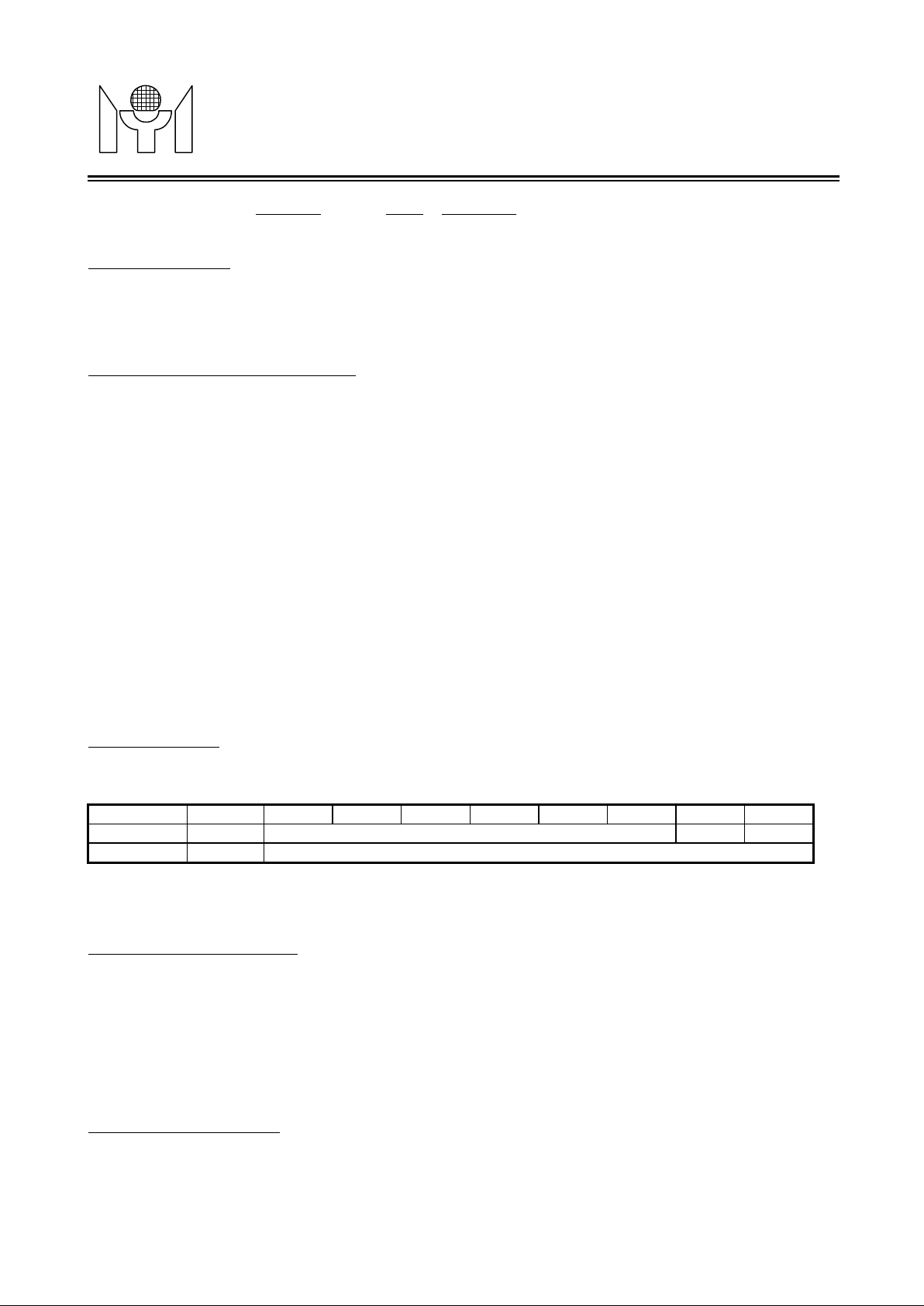
Reg name addr bi t7 bit6 bit5 b it4 bit3 bit 2 bi t1 bit0
ISPSLV
ISPEN
11. On-Screen Dis pl ay (OSD)
size is based on the information of pixel clock input cycle, double width control bit (DWE), and double
character width bit (CWS). The horizontal display center could be figured out according to the information of
horizontal starting position register (HORD) and OSDHS input. A horizontal displa y line includes 360 dots for
30 display characters and the remaining dots for blank region.
the leading edge of OSDHS is calculated using the following equation:
Horizontal delay time = (HORD * 6 +49) * P
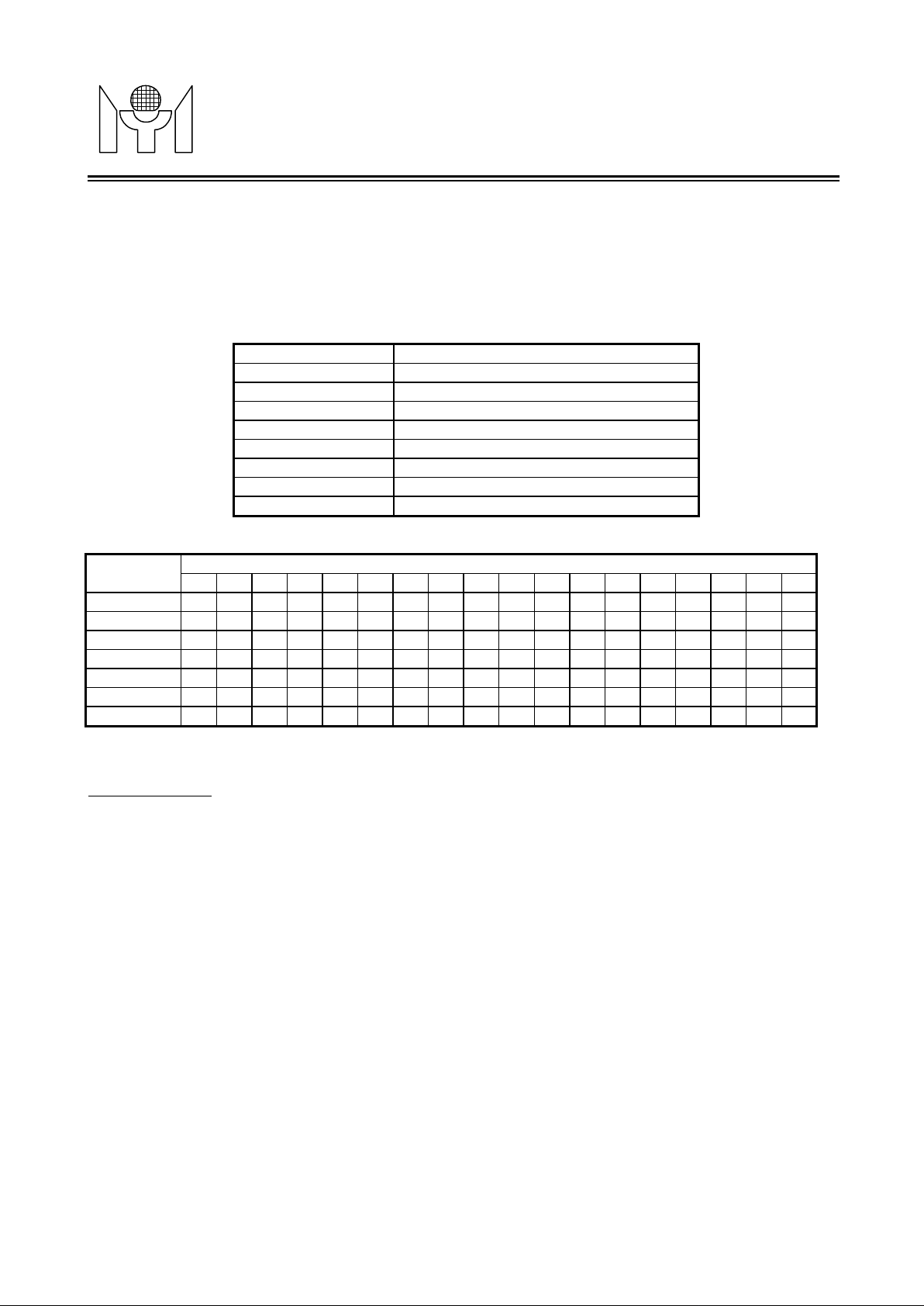
monitors. The vertical display size is calculated with the information of double character he ight bit (CHS),
character vertical height control register (CH6-CH0). The algorithms of repeating character line display are
Revision 1.0 - 18 - 2000/11/15
F0bh (w) ISP Slave address
F0ch (w)
” with
Page 19
MYSON
Repeat Line Weight of Character
The display RAM contains character address, attribute and row control registers. The display registers have
There are 4 registers to program display RAM: OSDRA, OSDCA, OSDDT0 and OSDDT1. OSDRA is the row
(bit 7 - bit 6) of OSDRA register are used to distinguish ADDRESS byte when the y are set to
ATTRIBUTE byte when they are set to
of display characters address. The MSB (bit 8) of display characters address will be equal to
while data byte is filled into OSDDT1; and OSDDT0 or OSDDT1 are the 8
The programming row (OSDRA) and column (OSDCA) address of display RAM will be incremented
Since bit 8 is fixed on OSDDT0 (OSDDT1) while programming ADDRESS byte, the continued OSDDT0
MTV230M
TECHNOLOGY
shown in the table below. The programmable vertical size ranges are 270 lines to maximum 2130 lines.
The vertical display center for full screen display could be figured out according to the information of vertical
starting position register (VERTD) and OSDVS input. The vertical display starting position from the leading
edge of OSDVS is calculated using the following equation:
Vertical delay time = (VERTD * 4 +1) * H , where H = one horizontal line display time
Repeat Line Number of character
Weight
+1 - - - - - - - - v - - - - - - - - +2 - - - - v - - - - - - - v - - - - +4 - - v - - - v - - - v - - - v - - -
+8 - v - v - v - v - v - v - v - v - +16 - v v v v v v v v v v v v v v v v +17 v v v v v v v v v v v v v v v v v +18 v v v v v v v v v v v v v v v v v v
Note: “v” means the nth line in the character would be repeated once, while “-“ means the nth line in the
character would not be repeated.
0 1 2 3 4 5 6 7 8 9 10 11 12 13 14 15 16 17
CH6 – CH0 Repeat Line Weight
CH6, CH5 = 11 +18*3
CH6, CH5 = 10 +18*2
CH6, CH5 = 0x +18
CH4 = 1 +16
CH3 = 1 +8
CH2 = 1 +4
CH1 = 1 +2
CH0 = 1 +1
Repeat Line #Repeat Lin e
(Rev 1.0)
11.3 Display RAM
450 locations which are allocated between (row 0, column 0) to (row14, colum n 29). Each display register
has its corresponding character address on ADDRESS bytes, and its corresponding color, blink bit,
background color on ATTRIBUTE bytes. The row control register is allocated at co lumn 30 from row 0 to row
14 of address bytes. It is used to set character size to each respective row. If double width character is
chosen, only even column characters could be displayed on screen and the odd column characters will be
hidden.
address; OSDCA is the column address; OSDDT0 and OSDDT1 are the programming data byte. The 2 MSB
byte is filled into OSDDT0, or “1”
LSB (bit 7 - bit 0) of display characters address.
automatically when MCU continues to update OSDDT0 or OSDDT1. It is used to save the program ROM
size of MCU while massive data update or full screen data change.
(OSDDT1) will be the same bank of lower 256 fonts (upper 256 fonts) until program another data byte
OSDDT1 (OSDDT0) register.
Revision 1.0 - 19 - 2000/11/15
“0, 1”. OSDDT0 and OSDDT1 are used to differentiate the MSB (bit 8)
“0, 0” and
”0“ while data
Page 20
MYSON
To program ADDRESS bytes and ATTRIBUTE bytes of the displa y RAM:
to determine the programming column address of the display RAM.
the display RAM and the post increment operation. Furthermore, the undefined locations in the display RAM
is applied. Furthermore, the undefined locations in display or user fonts RAM should be filled with dummy
Bytes of the Display RAM
of the Display RAM
MTV230M
TECHNOLOGY
Step 1. Write data into OSDRA to determine the programming row address of the display RAM. And define
Step 2. Write data into OSDCA
Step 3. Write to OSDDT0 or OSDDT1 the address or attribute of the character to be displayed on the
Step 4. Post increment operation is executed in the OSDCA (i.e. OSDCA ← OSDCA + 1) to make it point
It is the step 3 which triggers the load of OSDDT0 or OSDDT1 into the current OSDRA, OSDCA address of
should be filled with dummy data while post increment operation is executed.
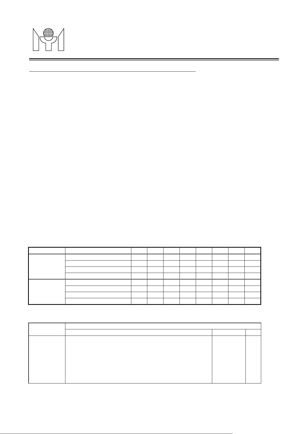
So there are three transmission formats shown as below:
Format (a) R - C - D −> R - C - D −> R - C - D …..
Format (b) R - C - D −> C - D −> C - D −> C - D …..
Format (c) R - C - D −> D −> D −> D −> D −> D …..
Where R= OSDRA (row address), C= OSDCA (column address), D= OSDDT0 or OSDDT1 (display data)
whether it is the row address of ADDRESS byte (bit7-bit6 = “0, 0”) or ATTRIBUTE byte (bit7-bit6 =
“0, 1”).
screen.
to the next display RAM location. Overflow of the OSDCA, i.e. overflow from 31, makes itself return
to 0 and makes post increment operation executed in the OSDRA (i.e. OSDR A ← OSDRA + 1).
Overflow of the OSDRA, i.e. overflow from 15, makes itself return to 0.
(Rev 1.0)
Format (a) is suitable for updating small amount of data which will be allocated with different row address
and column address. Format (b) is recommended for updating data that has same row address but different
column address. Massive data updating or full screen data change should use format (c) to increase
transmission efficiency. The row and column address will be increm ented automatically when the format (c)
data.
The Configuration of Transmission Formats
Address b7 b6 b5 b4 b3 b2 b1 b0
ADDRESS
Bytes of
Display Reg.
ATTRIBUTE
Bytes of
Display Reg.
(OSDRA)
OSDRA (row address)
OSDCA (column address) - - - C4 C3 C2 C1 C0
OSDDT0 (data, b8=0) D7 D6 D5 D4 D3 D2 D1 D0
OSDDT1 (data, b8=1) D7 D6 D5 D4 D3 D2 D1 D0
OSDRA (row address)
OSDCA (column address) - - - C4 C3 C2 C1 C0
OSDDT0 (data, b8=0) D7 D6 D5 D4 D3 D2 D1 D0
OSDDT1 (data, b8=1) D7 D6 D5 D4 D3 D2 D1 D0
ADDRESS
0 1 28 29 30 31
0
1
Character ADDRESS
13
14
0 0
0 1
Colu mn # (OSDCA)Row #
- - R3 R2 R1 R0
- - R3 R2 R1 R0
ROW
CTRL REG
R
E
S
E
R
V
E
D
Revision 1.0 - 20 - 2000/11/15
Page 21
MYSON
Bytes of the Display RAM
of the Display RAM
means low intensity in this row. 15-character foreground color is achievable by this bit.
ctive row. If double width character is chosen, only even
fonts are located from character address 496 to 511. Each character and symbol consists of 12x18 dots
matrix. The MTV230M font edit tools can be used to design the 512 characters and symbols by software.
MTV230M
TECHNOLOGY
ATTRIBUTE
Colu mn # (OSDCA)Row #
(OSDRA)
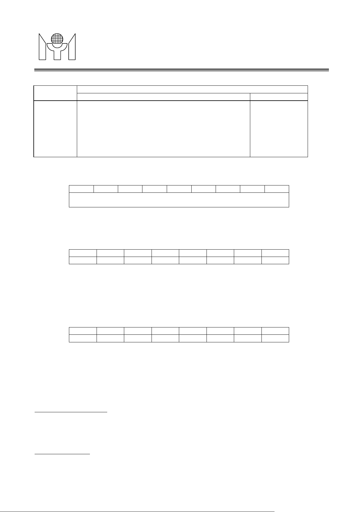
ADDRESS bytes:
CRADDR : Defines Flash-ROM OSD character address from address 0 to 511.
0 1 28 29 30 31
0
1
Character ATTRIBUTE
13
14
Display characters address (OSDRA 0 ~ 14, OSDCA 0 ~ 29),
B8 B7 B6 B5 B4 B3 B2 B1 B0
MSB LSB
(a) 0 ~ 479 => 480 standard fonts.
(b) 480 ~ 511 => 32 multi-color fonts.
CRADDR
(Rev 1.0)
RESERVED
Row control registers (OSDRA 0 ~ 14, OSDCA 30),
B7 B6 B5 B4 B3 B2 B1 B0
- - - - - RINT CHS CWS
RINT : The displayed character/symbol foreground color intensity control to the respective row. Setting this
bit to “0”
CHS : Defines double height character to the respective row.
CWS : Defines double width character to the respe
ATTRIBUTE bytes:
BGR, BGG, BGB : These three bits define the background color for its relative address character. If these
BLINK = 1 → Enables blink eff ect for its relative address character. And the blinking is alternate per 32
R, G, B : These three bits are used to specify their relative address character colors.
11.4 Character Flash-ROM
MTV230M character flash-ROM contains 512 characters and symbols including 496 standard fonts and 16
multi-color fonts. The 496 standard fonts are located from character address 0 to 495. And the multi-color
column characters could be displayed on screen and the odd column characters will be hidden.
Display character attribute (OSDRA 0 ~ 14, OSDCA 0 ~ 29),
B7 B6 B5 B4 B3 B2 B1 B0
- BGR BGG BGB BLINK R G B
three bits are set to (0, 0, 0), no background will be shown (transparent). Theref ore, a
total of 7 background colors can be selected.
vertical frames.
= 0 → Disables blink effect for its relative address character.
11.5 Multi-color Font
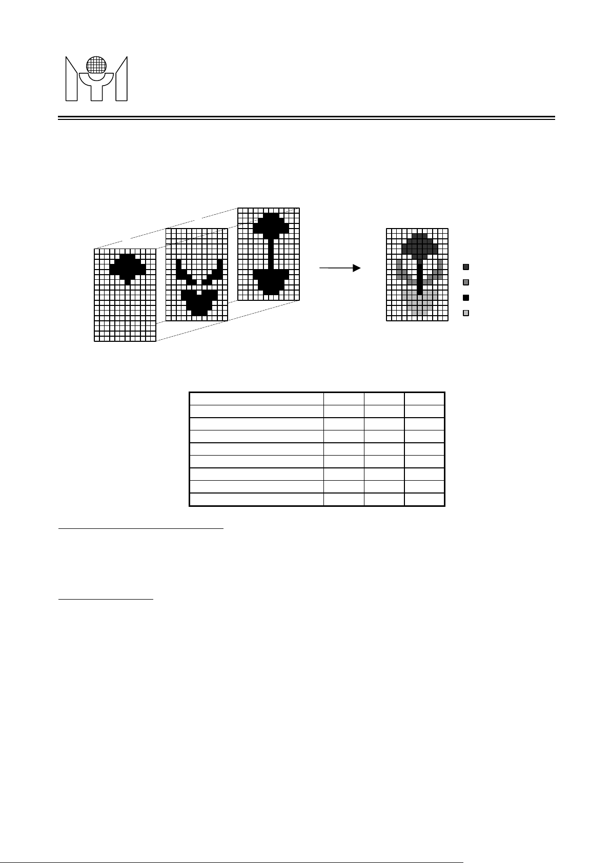
The color fonts comprise three different R, G, B fonts. When the code of color font is accessed, the separate
Revision 1.0 - 21 - 2000/11/15
Page 22
MYSON
The window size and position controls are specified in W1ROW, W1COL, W2ROW, W2COL, W3ROW,
W3COL, W4ROW and W4COL registers. And window 1 has the highest priority, and window 4 has the least,
MTV230M
TECHNOLOGY
R/G/B dot pattern is output to corresponding R/G/B output. See figure below for the sample displayed color
font.
Note: No black color can defined in color font, black window or background underline the color font can make
the dots become black in color.
B
G
R
Example of Multi-colo r Font
The Multi-color Font Color Selection
R G B
Background Color 0 0 0
Blue 0 0 1
Green 0 1 0
Cyan 0 1 1
Red 1 0 0
Magenta 1 0 1
Yellow 1 1 0
White 1 1 1
(Rev 1.0)
Magenta
Green
Blue
Cyan
11.6 Luminance & Border Generator
There are 3 shift registers included in the design which can shift out of luminance and border dots to color
encoder. The bordering and shadowing feature is configured in this block. For bordering effect, the character
will be enveloped with blackedge on four sides. For shadowing effect, the character is enveloped with
blackedge for right and bottom sides only.
11.7 Window Control
when two windows are overlapping.
The window shadow width and height controls are specified in WINSW and WINSH registers. And each
shadow has the same priority with its corresponding window.
Revision 1.0 - 22 - 2000/11/15
Page 23
MYSON
WINT
WSHD
WINT
WSHD
WINT
WSHD
WINT
WSHD
RSPACE
WENclr
WW41
WW40
WW31
WW30
WW21
WW20
WW11
WW10
WH41
WH40
WH31
WH30
WH21
WH20
WH11
WH10
Next 9-bit data will be written into ADDRESS b yte.
(w) : Window 1 control registers.
the corresponding window display
Enables the relative background window 1 display.
MTV230M
TECHNOLOGY
11.8 OSD Processor registers
Reg name addr bit 7 bit6 bi t5 bit4 bit3 bit2 bit1 bit0
OSDRA
OSDCA
OSDDT0
OSDDT1
W1ROW
W1COL
W1COL
W2ROW
W2COL
W2COL
W3ROW
W3COL
W3COL
W4ROW
W4COL
W4COL
VERTD
HORD
CH
OSDCON
OSDCON
CHSC
FSSTP
WINSW
WINSH
WINSC
WINSC
XDEL
FA0h (w) A1 A0 - - R3 R2 R1 R0
FA1h (w) - - - C4 C3 C2 C1 C0
FA2h (w) D7 D6 D5 D4 D3 D2 D1 D0
FA3h (w) D7 D6 D5 D4 D3 D2 D1 D0
FC0h (w) Row start address Row end address
FC1h (w) Column start address WEN
FC2h (w) Column end address R G B
FC3h (w) Row start address Row end address
FC4h (w) Column start address WEN
FC5h (w) Column end address R G B
FC6h (w) Row start address Row end address
FC7h (w) Column start address WEN
FC8h (w) Column end address R G B
FC9h (w) Row start address Row end address
FCAh (w) Column start address WEN
FCBh (w) Column end address R G B
FCCh (w) Vertical delay
FCDh (w) Horizontal delay
FCEh (w) - Character height
FD0h (w) - - - Row to row spacing
FD1h (r/w) OSDEN BSEN Shadow FBEN Blend
FD2h (r/w) - - - DWE HSP VSP - -
FD3h (w) CSR CSG CSB
FD4h (w) FSW - - - - FSR FSG FSB
FD5h (w)
FD6h (w)
FD7h (w) - R1 G1 B1 - R2 G2 B2
FD8h (w) - R3 G3 B3 - R4 G4 B4
FD9h (w) - - - - - D2 D1 D0
(Rev 1.0)
RAMclr FBKGC
OSDRA (w) :
R3-R0 :This is the row address of the display RAM that next 9-bit data should be written into.
A1-A0 = (0, 0) →
= (0, 1) → Next 9-bit data will be written into ATTRIBUTE byte.
OSDCA (w) : This is the column address of the display RAM that next 9-bit data should be written into.
OSDDT0 (w) : The MSB (bit 8) = 0, 8 LSB (bit 7 ~ bit 0) = OSDDT0. The 9-bit data will be written into current
(OSDRA, OSDCA) address of the display RAM. It will also trigger the post increment
operation of OSDRA and OSDCA.
OSDDT1 (w) : The MSB (bit 8) = 1, 8 LSB (bit 7 ~ bit 0) = OSDDT1. The 9-bit data will be written into current
(OSDRA, OSDCA) address of the display RAM. It will also trigger the post increment
operation of OSDRA and OSDCA.
W1ROW, W1COL
Row (column) start (end) address : These registers are used to specify the window 1 size. It should
WEN :
Revision 1.0 - 23 - 2000/11/15
be noted that when the start address is greater than end address,
will be disabled.
Page 24

MYSON
(w) : Window 2 control registers.
Enables the relative background window 2 display.
(w) : Window 3 control registers.
s the relative background window 3 display.
(w) : Window 4 control registers.
Enables the relative background window 4 display.
ifies the color intensity of the background window 4. Setting this bit to
of each step is 4 horizontal display lines. The starting position is calculated as (VERTD*4 + 1)
MTV230M
TECHNOLOGY
WINT : Specifies the color intensity of the background window 1. Setting this bit to “0” means low
intensity.
WSHD : Enables shadowing on the window 1.
R, G, B : Specifies the color of the relative background window 1.
W2ROW, W2COL
Row (column) start (end) address : These registers are used to specify the window 2 size.
WEN :
WINT : Specifies the color intensity of the background window 2. Setting this bit to “0” means low
intensity.
WSHD : Enables shadowing on the window 2.
R, G, B : Specifies the color of the relative background window 2.
W3ROW, W3COL
Row (column) start (end) address : These registers are used to specify the window 3 size.
WEN : Enable
WINT : Specifies the color intensity of the background window 3. Setting this bit to “0” means low
intensity.
WSHD : Enables shadowing on the window 3.
R, G, B : Specifies the color of the relative background window 3.
W4ROW, W4COL
Row (column) start (end) address : These registers are used to specify the window 4 size.
WEN :
WINT : Spec
intensity.
WSHD : Enables shadowing on the window 4.
R, G, B : Specifies the color of the relative background window 4.
(Rev 1.0)
“0” means low
VERTD (w) : Specifies the starting position for vertical displa y. The total steps are 256, and the increment
horizontal display lines. The initial value is 4 after power up.
HORD (w) : Specifies the starting position for horizontal display. The total steps are 256, and the
increment of each step is 6 dots. The starting position is calculated as (HORD*6 + 49)
horizontal display dots. The initial value is 15 after power up.
CH (w) : Defines the character vertical height, the height is programmable from 18 to 71 lines. The
character vertical height is at least 18 lines if the content of CH6-CH0 is less than 18. For
example, when the content is “2”, the character vertical height is regarded as equal to 20
lines. And if the content of CH4-CH0 is greater than or equal to 18, it will be regarded as
equal to 17. See table list in section 11.1 for detail description of this operation.
RSPACE (w) : Defines the row to row spacing in unit of horizontal line. Extra RSPACE horizontal lines will be
appended below each display row, and the maximum space is 31 lines. The initial value is 0
after power up.
OSDCON (r/w) : OSD control registers.
OSDEN= 1 → Activates the OSD operation.
= 0 → Disables the OSD operation.
BSEN = 1 → Enables the character bordering or shadowing effect.
= 0 → Disables bordering and shadowing effect.
Shadow = 1 → Selects the character shadowing effect if BSEN bit is set to “1”.
= 0 → Selects the character bordering effect if BSEN bit is set to “1”.
FBEN = 1 → Enables the fade-in/fade-out or blending-in/blending-out ef fect when OSD is
Revision 1.0 - 24 - 2000/11/15
Page 25
MYSON
Clears all ADDRESS bytes, BGR, BGG, BGB and BLINK bits of display RAM.
Accepts negative polarity OSDHS input.
Accepts negative polarity OSDVS input.
Determines the shadow height of window 4 when W SHD bit of window 4 is enabled.
Determines the shadow height of window 3 when W SHD bit of window 3 is enabled.
es the shadow height of window 2 when WSHD bit of window 2 is enabled.
Determines the shadow height of window 1 when W SHD bit of window 1 is enabled.
MTV230M
TECHNOLOGY
turned on from off state or vice versa.
= 0 → Disables the fade-in/fade-out and blending-in/blending-out effect.
Blend = 1 → Selects the blending-in/blending-out effect if FBEN bit is set to “1”.
= 0 → Selects the fade-in/fade-out effect if FBEN bit is set to “1”.
WENclr= 1 → Clears all WEN bits of window control registers.
= 0 → Normal.
RAMclr = 1 →
= 0 → Normal.
FBKGC = 1 → Pin FBKG outputs is high only during the displaying of characters.
DWE = 1 → Enables double width. The OSD menu will change to half resolution for double
HSP = 1 → Accepts positive polarity OSDHS input.
VSP = 1 → Accepts positive polarity OSDVS input.
CHSC (w) : Character shadow color select registers.
CSR, CSG, CSB : Defines the color of bordering or shadowing color on characters.
= 0 → Pin FBKG outputs is high during the displaying of characters or windows.
character width. And the number of pixels of each line should be even.
= 0 → Normal.
= 0 →
= 0 →
(Rev 1.0)
FSSTP (w) : Full screen self-test pattern registers.
FSW = 1 → Enables full screen self-test pattern and force pin FBKG outputs high to disable
video RGB.
= 0 → Disables full screen self-test pattern.
FSR, FSG, FSB : Defines the color of full screen self-test pattern.
WINSW (w) : Window shadowing width control registers.
WW41, WW40 : Determines the shadow width of window 4 when WSHD bit of window 4 is enabled.
Please refer to the table below for more details.
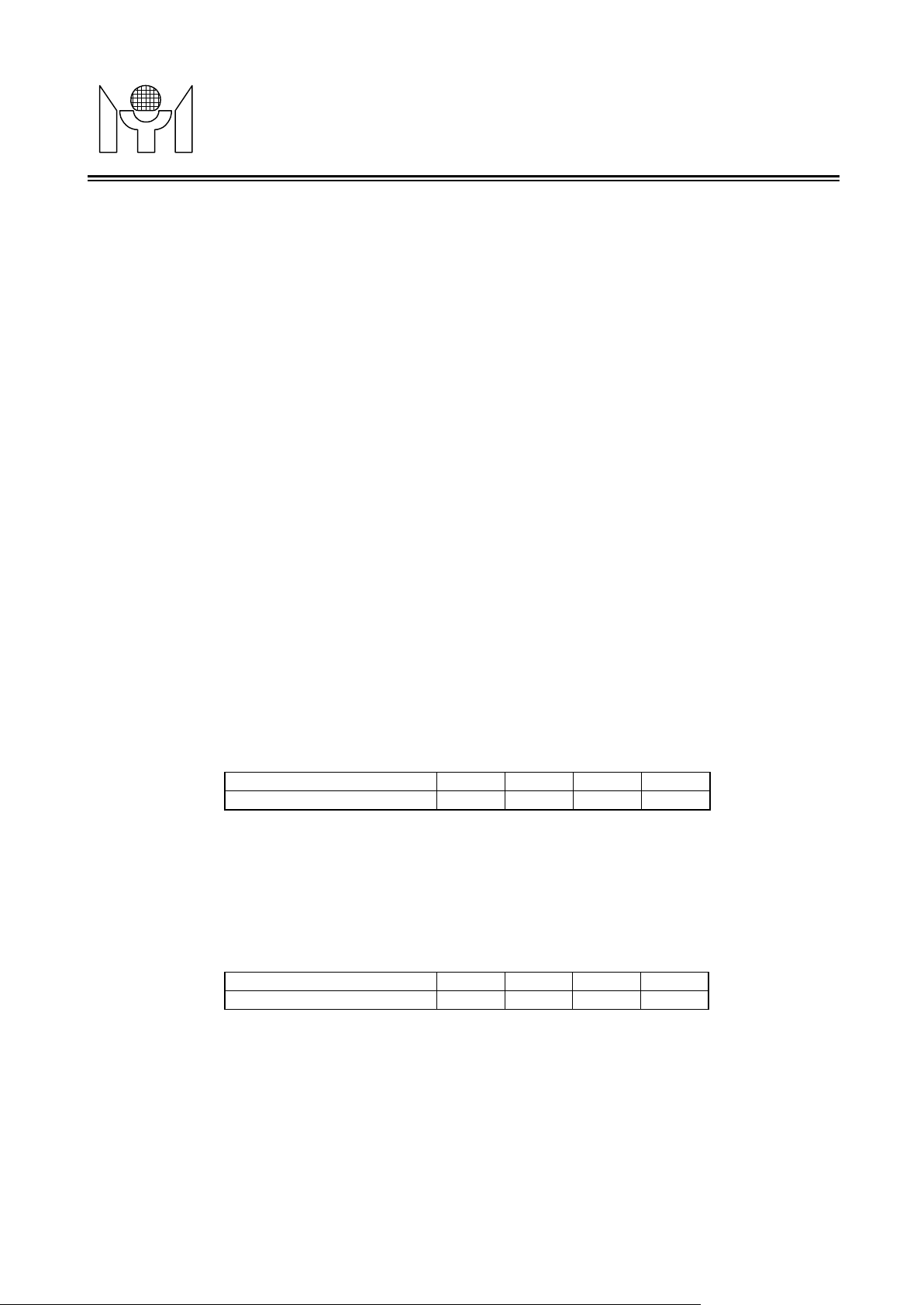
(WW41, WW40) (0, 0) (0, 1) (1, 0) (1, 1)
Shadow Width (unit in Pixel) 2 4 6 8
WW31, WW30 : Determines the shadow width of window 3 when WSHD bit of window 3 is enabled.
WW21, WW20 : Determines the shadow width of window 2 when WSHD bit of window 2 is enabled.
WW11, WW10 : Determines the shadow width of window 1 when WSHD bit of window 1 is enabled.
WINSH (w) : Window shadowing height control registers.
WH41, WH40 :
Please refer to the table below for more details.
(WH41, WH40) (0, 0) (0, 1) (1, 0) (1, 1)
Shadow Height (unit in Line) 2 4 6 8
WH31, WH30 :
WH21, WH20 : Determin
WH11, WH10 :
Revision 1.0 - 25 - 2000/11/15
Page 26
MYSON
Note:
N Horizontal lines
N Horizontal lines
MTV230M
TECHNOLOGY
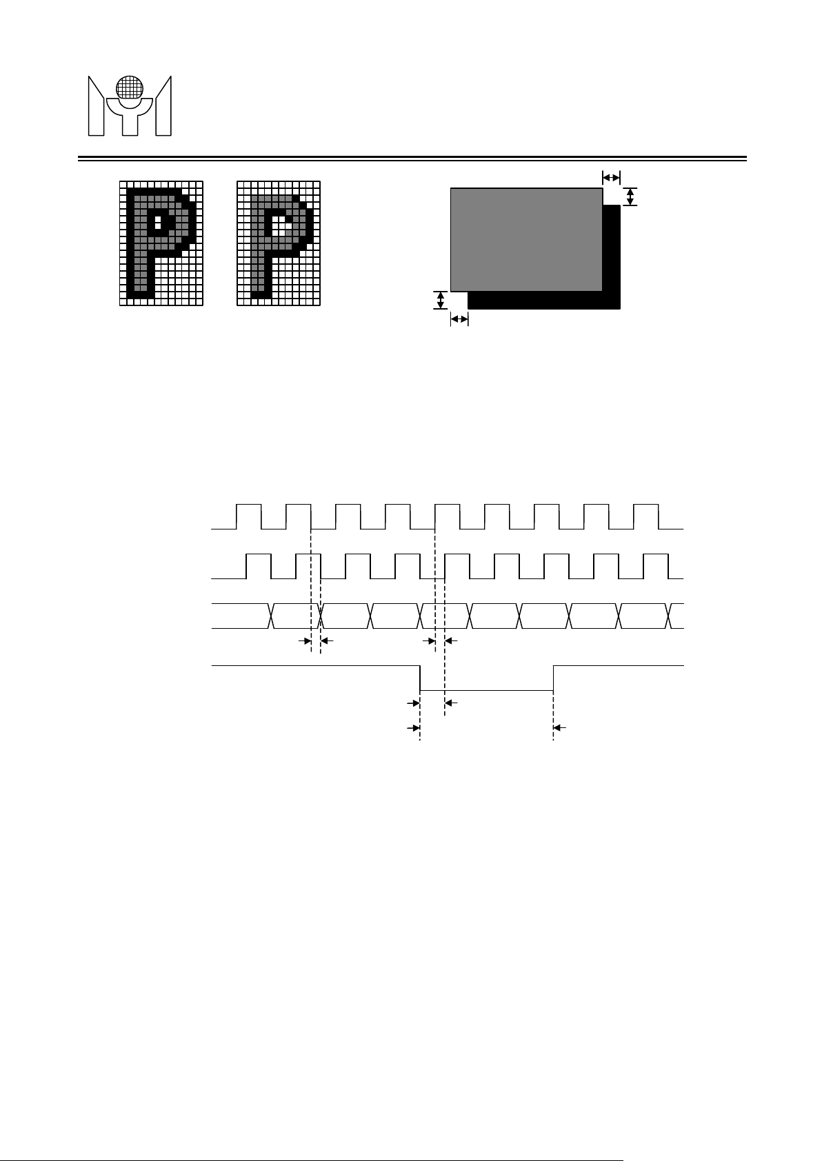
Bordering Shadowing
Character Bord ering and Shadowin g and Shadowing on Window
WINSC (w) : Window shadowing color control registers.
R1, G1, B1 : Define the shadowing color of window 1.
R2, G2, B2 : Define the shadowing color of window 2.
R3, G3, B3 : Define the shadowing color of window 3.
R4, G4, B4 : Define the shadowing color of window 4.
XDEL (w) : Rout, Gout, Bout, FBKG and INT outputs delay reference to pin XIN input falling edge control
registers.
M Pixels
(Rev 1.0)
M Pixels
M and N are defin ed
by the registers of
WINSW and WINSH.
OSD output
tPD
tPD
tSETUP
tHOLD
Revision 1.0 - 26 - 2000/11/15
Page 27
MYSON
WadrB
WadrA
SLVAADR
SLVBADR
Write 93h to enable ISP Mode
WCLR
WDT2
WDT1
WDT0
Pulse width of PWM DAC 0
Pulse width of PWM DAC 1
Pulse width of PWM DAC 2
Pulse width of PWM DAC 3
PADMOD
PADMOD
PADMOD
PADMOD
PWMF
MTV230M
TECHNOLOGY
(Rev 1.0)
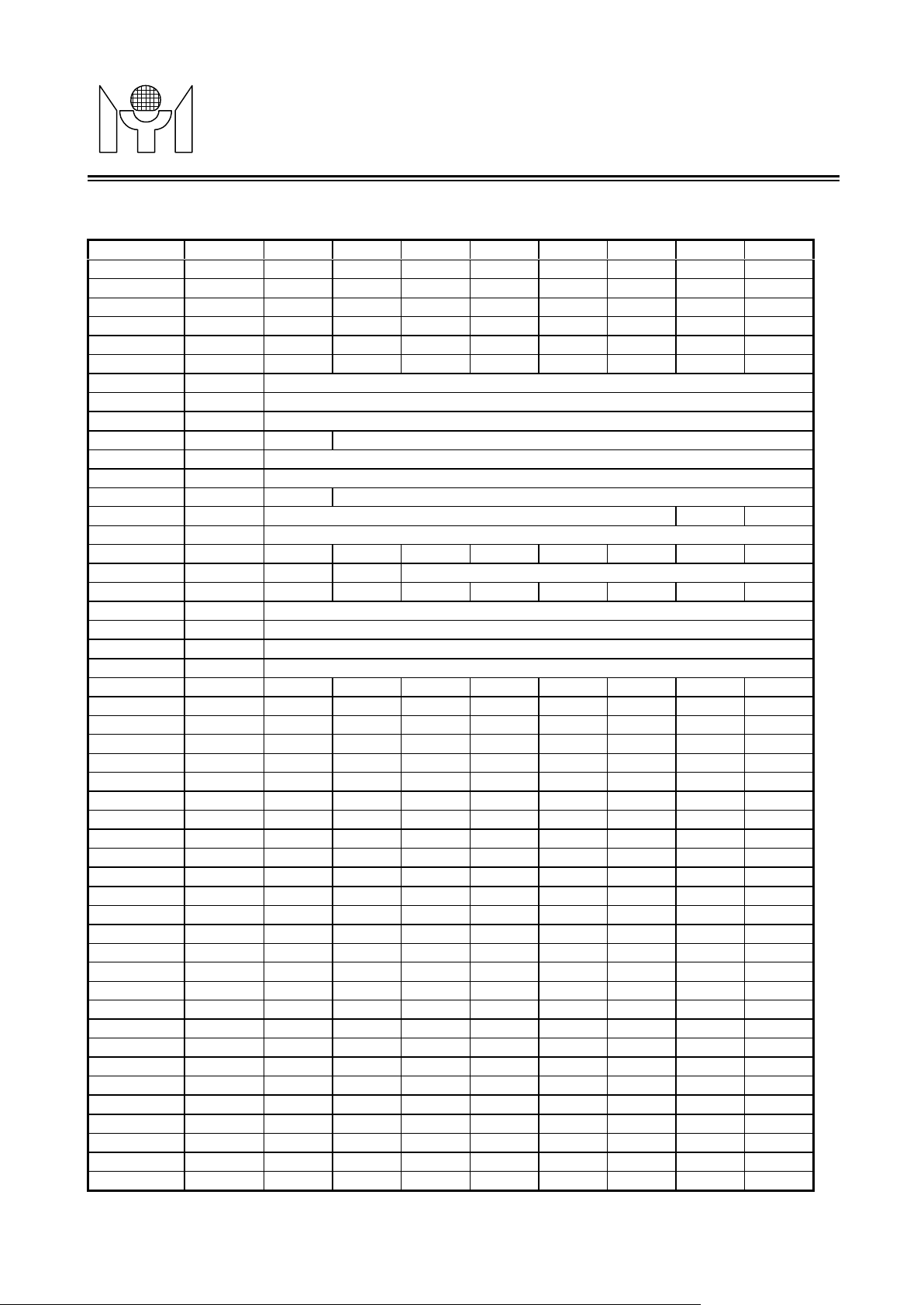
Memor y Map of XFR
Reg name addr bit7 bit6 bit5 bit4 bit3 bit2 bit 1 bi t0
IICCTR
IICSTUS
IICSTUS
INTFLG
INTFLG
INTEN
MBUF
RCABUF
TXABUF
RCBBUF
TXBBUF
ISPSLV
ISPEN
ADC
ADC
WDT
DA0
DA1
DA2
DA3
PORT6
PORT6
PORT6
OPTION
PORT4
PORT4
PORT4
PORT4
PORT4
PORT4
PORT4
PORT4
PORT5
PORT5
PORT5
PORT5
PORT5
PORT5
PORT5
PORT5
HVSTUS
HCNTH
HCNTL
Revision 1.0 - 27 - 2000/11/15
F00h (r/w) MAckO P S
F01h (r)
F02h (r) MAckIn
F03h (r) TXBI RCBI SlvBMI TXAI RCAI SlvAMI MbufI
F03h (w) SlvBMI SlvAMI MbufI
F04h (w) ETXBI ERCBI ESlvBMI ETXAI ERCAI ESlvAMI EMbufI
F05h (r/w) Master IIC receive/transmit data buffer
F06h (r) Slave A IIC receive buffer
F06h (w) Slave A IIC transmit buffer
F07h (w) ENSlvA Slave A IIC address
F08h (r) Slave B IIC receive buffer
F08h (w) Slave B IIC transmit buffer
F09h (w) ENSlvB Slave B IIC address
F0bh (w) ISP Slave address
F0ch (w)
F10h (w) ENADC SADC3 SADC2 SADC1 SADC0
F10h (r) ADC convert Result
F18h (w) WEN
F20h (r/w)
F21h (r/w)
F22h (r/w)
F23h (r/w)
F28h(w) P60
F29h(w) P61
F2Ah(w) P62
F2Bh (w) HIICE IIICE HVE HclpE FclkE P62E
F2Ch (w) DA3E DA2E DA1E DA0E AD3E AD2E AD1E AD0E
F2Dh (w) P47oe P46oe P45oe P44oe P43oe P42oe P41oe P40oe
F2Eh (w) P57oe P56oe P55oe P54oe P53oe P52oe P51oe P50oe
F2Fh (w)
F30h(r/w) P40
F31h(r/w) P41
F32h(r/w) P42
F33h(r/w) P43
F34h(r/w) P44
F35h(r/w) P45
F36h(r/w) P46
F37h(r/w) P47
F38h(r/w) P50
F39h(r/w) P51
F3Ah(r/w) P52
F3Bh(r/w) P53
F3Ch(r/w) P54
F3Dh(r/w) P55
F3Eh(r/w) P56
F3Fh(r/w) P57
F40h (r) CVpre Hpol Vpol Hpre Vpre Hoff Voff
F41h (r) Hovf HF13 HF12 HF11 HF10 HF9 HF8
F42h (r) HF7 HF6 HF5 HF4 HF3 HF2 HF1 HF0
DIV253 SlvAbs1 SlvAbs0 ENSCL Msel MIICF1 MIICF0
SlvRWB SAckIn SLVS SlvAlsb1 SlvAlsb0
Page 28
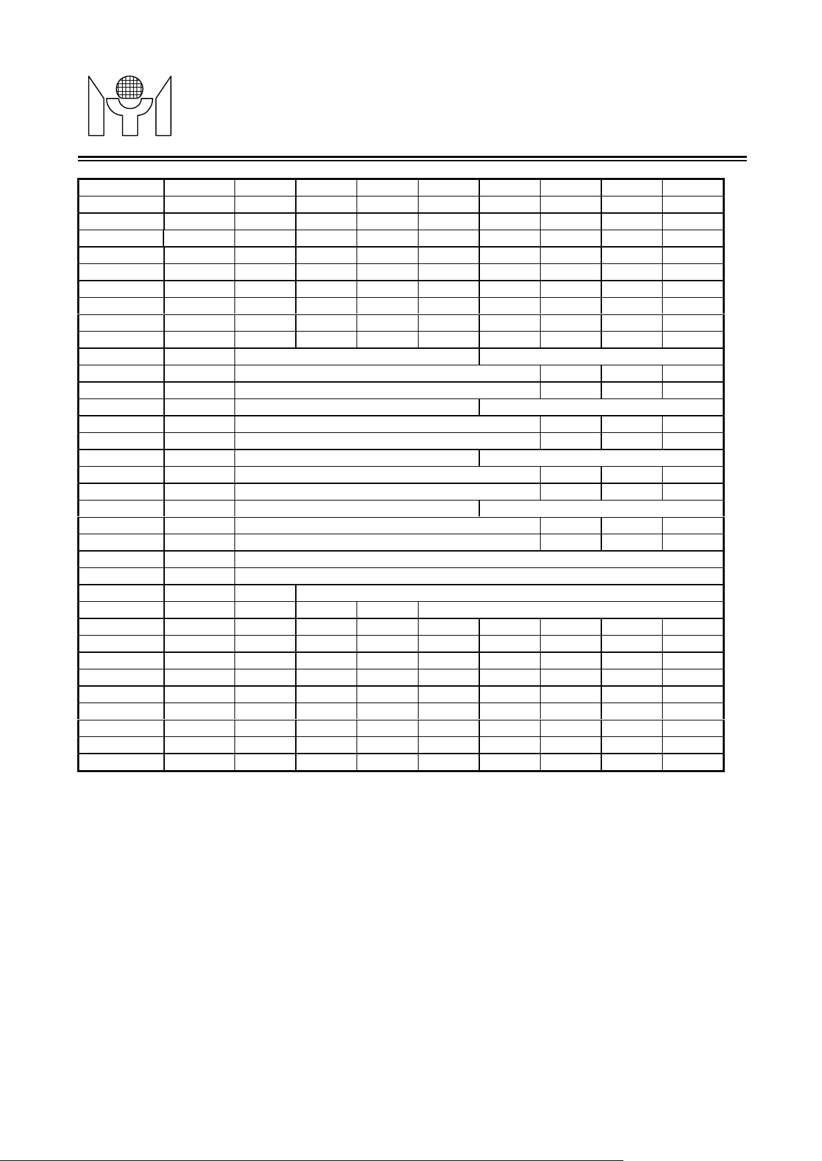
MYSON
EVsync
WINT
WSHD
WINT
WSHD
WINT
WSHD
WINT
WSHD
WENclr
WW41
WW40
WW31
WW30
WW21
WW20
WW11
WW10
WH41
WH40
WH31
WH30
WH21
WH20
WH11
WH10
MTV230M
VCNTH
VCNTL
HVCTR0
HVCTR3
INTFLG
INTEN
OSDRA
OSDCA
OSDDT0
OSDDT1
W1ROW
W1COL
W1COL
W2ROW
W2COL
W2COL
W3ROW
W3COL
W3COL
W4ROW
W4COL
W4COL
VERTD
HORD
CH
RSPACE
OSDCON
OSDCON
CHSC
FSSTP
WINSW
WINSH
WINSC
WINSC
XDEL
TECHNOLOGY
F43h (r) Vovf VF11 VF10 VF9 VF8
F44h (r) VF7 VF6 VF5 VF4 VF3 VF2 VF1 VF0
F40h (w) C1 C0 NoHins HBpl VBpl
F43h (w) CLPEG CLPPO CLPW2 CLPW1 CLPW0
F48h (r/w) HPRchg VPRchg HPLchg VPLchg HFchg VFchg Vsync
F49h (w) EHPR EVPR EHPL EVPL EHF EVF
FA0h (w) A1 A0 - - R3 R2 R1 R0
FA1h (w) - - - C4 C3 C2 C1 C0
FA2h (w) D7 D6 D5 D4 D3 D2 D1 D0
FA3h (w) D7 D6 D5 D4 D3 D2 D1 D0
FC0h (w) Row start address Row end address
FC1h (w) Column start address WEN
FC2h (w) Column end address R G B
FC3h (w) Row start address Row end address
FC4h (w) Column start address WEN
FC5h (w) Column end address R G B
FC6h (w) Row start address Row end address
FC7h (w) Column start address WEN
FC8h (w) Column end address R G B
FC9h (w) Row start address Row end address
FCAh (w) Column start address W EN
FCBh (w) Colum n end address R G B
FCCh (w) Vertical delay
FCDh (w) Horizontal delay
FCEh (w) - Character height
FD0h (w) - - - Row to row spacing
FD1h (r/w) OSDEN BSEN Shadow FBEN Blend
FD2h (r/w) - - - DWE HSP VSP - -
FD3h (w) CSR CSG CSB
FD4h (w) FSW - - - - FSR FSG FSB
FD5h (w)
FD6h (w)
FD7h (w) - R1 G1 B1 - R2 G2 B2
FD8h (w) - R3 G3 B3 - R4 G4 B4
FD9h (w) - - - - - D2 D1 D0
(Rev 1.0)
RAMclr FBKGC
Test Mode Conditi o n
In normal application, users should avoid the MTV230M entering its test m ode, outlined as follow:
Test Mode A: RESET=1 & P5.7=1 & P5.6=0 & P5.5=1 & P5.4=0
Test Mode B: RESET's falling edge & P5.7=0 & P5.6=1 & P5.5=1 & P5.4=0
Writer Mode: RESET=1 & P5.5=0 & P5.4=1 & “special serial data on OSDVS”
Revision 1.0 - 28 - 2000/11/15
Page 29
MYSON
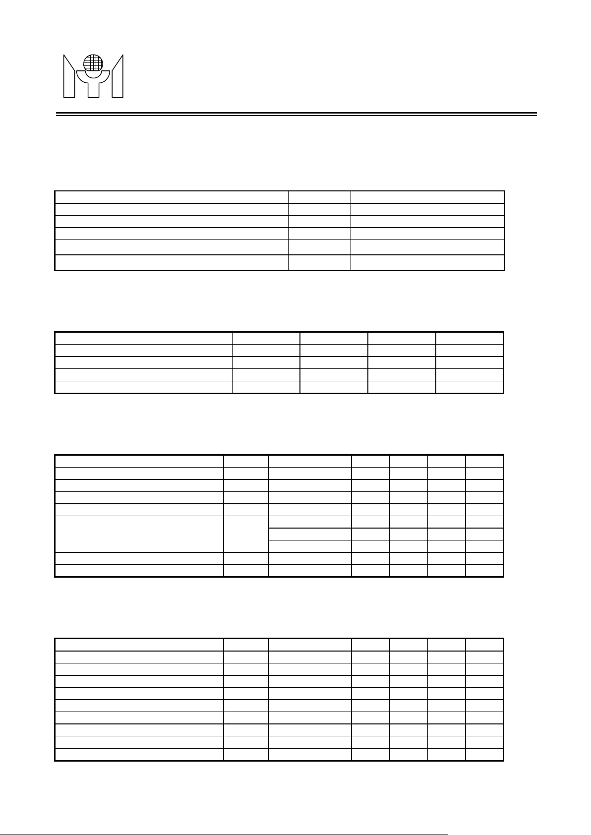
ELECTRICAL PARA METERS
1. Absolu t e Maximum Rating s
Maximum Supply Voltage
2. Allowable Operating Condit io ns
Power Supply Current
4. AC Characterist ic s
PWM DAC Frequency
tVIPW
tVCPW
MTV230M
TECHNOLOGY
at: Ta= 0 to 70 oC, VSS=0V
Name Symbol Range Unit
VDD -0.3 to +4.0 V
Maximum Input Voltage (except Open Drain Pin)) Vin -0.3 to VDD+0.3 V
Maximum Input Voltage (Open Drain pin) Vin 6 V
Maximum Operating Temperature Topg 0 to +70 o
Maximum Storage Temperature Tstg -25 to +125 o
at: Ta= 0 to 70 oC, VSS=0V
Name Symbol Min . Max. Unit
Supply Voltage VDD 3.0 3.6 V
Input "H" Voltage Vih 0.7 x VDD VDD +0.3 V
Input "L" Voltage Vil -0.3 0.25 x VDD V
Operating Freq. Fopg - 15 MHz
(Rev 1.0)
C
C
3. DC Characteri s t i c s
at: Ta=0 to 70 oC, VDD=5.0V, VSS=0V
Name Symbol Condition Min. Typ. Max. Unit
Output "H" Voltage, open drain pin Voh1 Ioh=0uA 2.7 V
Output "H" Voltage, 8051 I/O port pin Voh2 Ioh=-50uA 2.7 V
Output "H" Voltage, CMOS Voh3 Ioh=-5mA 2.7 V
Output "L" Voltage Vol Iol=8mA 0.4 V
Active 18 4 mA
Idd
RST Pull-Down Resistor Rrst VDD=3.3V 100 250 Kohm
Pin Capacitance Cio 15 pF
at: Ta=0 to 70 oC, VDD=5.0V, VSS=0V
Name Symbol Condition Min. Typ. Max. Unit
Crystal Frequency fXtal 12 MHz
fDA fXtal=12MHz 46.875 94.86 KHz
HS input pulse Width tHIPW fXtal=12MHz 0.3 8 uS
VS input pulse Width
H+V to Vblank output delay tVVBD fXtal=12MHz 8 uS
VS pulse width in H+V signal
SDA to SCL setup time tDCSU 200 ns
SDA to SCL hold time tDCH 100 ns
SCL high time tSCLH 500 ns
Revision 1.0 - 29 - 2000/11/15
Idle 1.3 4.0 mA
Power-Down 50 80 uA
fXtal=12MHz 3 uS
FXtal=12MHz 20 uS
Page 30
MYSON
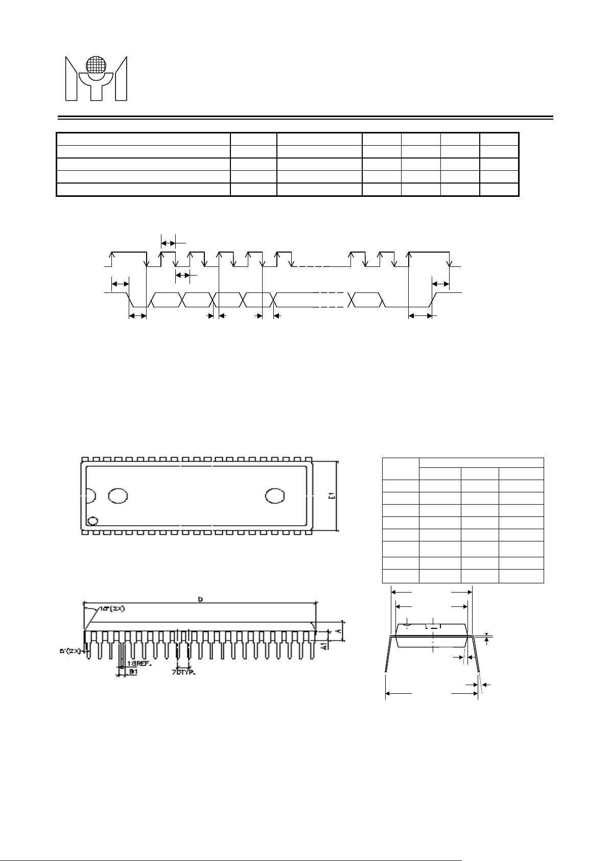
PACKAGE DIMENSION
MTV230M
TECHNOLOGY
(Rev 1.0)
SCL low time tSCLL 500 ns
START condition setup time tSU:STA 500 ns
START condition hold time tHD:STA 500 ns
STOP condition setup time tSU:STO 500 ns
STOP condition hold time tHD:STO 500 ns
t
SCKH
t
t
SU:STO
HD:STO
t
SU:STA
t
HD:STA
t
SCKL
t
DCSU
t
DCH
Data int er f ace ti min g (I2C)
1. 42 pin SDIP Unit: mm
Symbol
Dimension in mm
Min No m Max
A 3.937 4.064 4.2
A1 1.78 1.842 1.88
B1 0.914 1.270 1.118
D 36.78 36.83 36.88
E1 13.945 13.970 13.995
F 15.19 15.240 15.29
eB 15.24 16.5 10 17.78
θ 0° 7.5° 15°
15.494mm +/-
0.254
13.868mm +/-
0.102
5o~7
16.256mm +/-
0.508
0
6o +/-
3
0.254m
m
+/-0.102
o
Revision 1.0 - 30 - 2000/11/15
Page 31
MYSON
MTV230M
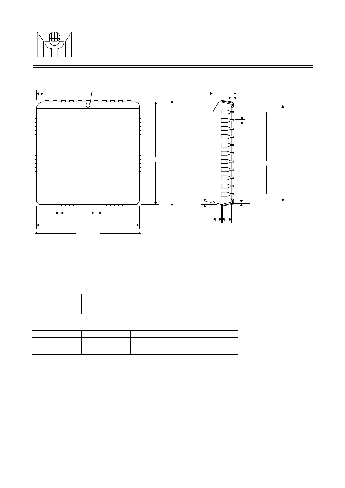
2. 44 pin PLCC Unit:
0
0.045*45
0.050 TYP.
0.653 +/-0.003
0.690 +/-0.005
TECHNOLOGY
PIN #1 HOLE
0.690 +/-0.005
0.653 +/-0.003
0.026~0.032 TYP.
0.180 MAX.
0.013~0.021 TYP.
70TYP.
0.070 0.070
(Rev 1.0)
0.020 MIN.
0.610 +/-0.02
0.500
0.010
Ordering Inform ation
Standard Configurations:
Prefix Part Typ e Package Type ROM Size (K)
MTV 230M
S: SDIP
V: PLCC
Part Numbers:
Prefix Part Typ e Pack age Type ROM Size (K)
MTV 230M V 64
MTV 230M F 64
64
Revision 1.0 - 31 - 2000/11/15
 Loading...