

Page 1
MYSON
MTV012E
TECHNOLOGY
8051 Embedded CRT Monitor Controller
OTP Version
FEATURES
8051 core.
256 bytes internal RAM.
8K bytes program EPROM.
14 channels 12V open drain PWM DAC, 10 dedicated channels and 4 channels shared with I/O pin.
20 bi-direction I/O pin, 12 dedicated pin, 4 shared with DAC, 4 shared with DDC/IIC interface.
3 output pin shared with H/V sync output and self test output pins.
SYNC processor for composite separation, polarity and frequency check, and polarity adjust.
Built-in monitor self test pattern generator.
Built-in Low Power Reset circuit.
IIC interface for DDC1/DDC2B and EEPROM, only one EEPROM needed to store DDC1/DDC2B and
display mode information.
Watch dog timer with programmable interval.
40 pin PDIP package.
GENERAL DESCRIPTION
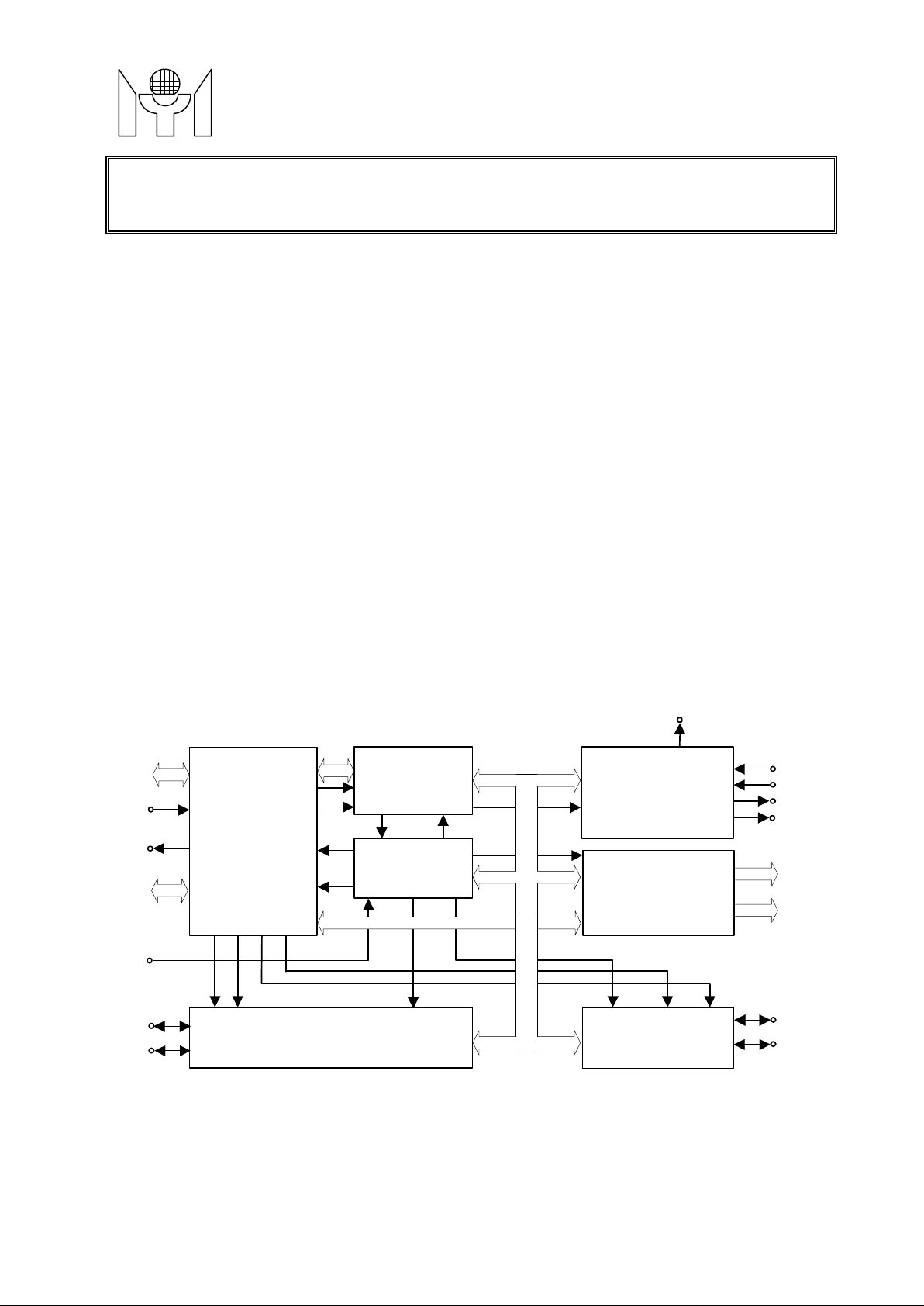
The MTV012E micro-controller is an 8051 CPU core-embedded device specially tailored to CRT monitor
applications. It includes an 8051 CPU core, 256-byte SRAM, 14 built-in PWM DACs, DDC1/DDC2B
interface, 24Cxx series EEPROM interface and an 8K-byte internal program EPROM.
BL OCK DIAGRAM
STOUT
P1.0-7
X1
X2
P2.0-3
P3.0-P3.2
8051
CORE
P3.4
P0.0-7
RD
WR
INT1
RST
P2.4-7
P0.0-7
XFR
RD
WR
WATCH-DOG
TIMER
RST
H/VSYNC
CONTROL
14 CHANNEL
PWM DAC
HSYNC
VSYNC
HBLANK
VBLANK
DA0-9
DA10-13
HSCL
HSDA
This datasheet contains new product information. Myson Technology reserv es the rights to modify the product specification
without notice. No liability is assumed as a result of the use of this product. No rights under any patent accompany the sale of the
product.
DDC 1/2 B & FIFO
INTERFACE
IIC INTERFACE
MTV012E Revision 1.2 12/23/1998
1/14
ISCL
ISDA
Page 2
MYSON
TECHNOLOGY
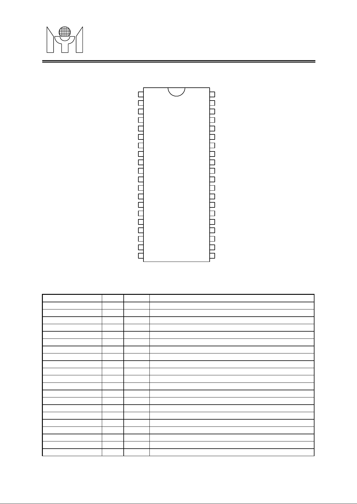
1.0 PIN CONNECTION
MTV012E
P1.0
P1.1
P1.2
P1.3
P1.4
P1.5
P1.6
P1.7
RST
HSCL/P3.0/Rxd
HSDA/P3.1/Txd
ISDA/P3.2/INT0
HSYNC
ISCL/P3.4/T0
VSYNC
HBLANK/P4.1
VBLANK/P4.0
X2
X1
VSS
MTV012E
VDD
DA0
DA1
DA2
DA3
DA4
DA5
DA6
DA7
DA8
DA9
STOUT/P4.2
DA10/P2.7
DA11/P2.6
DA12/P2.5
DA13/P2.4
P2.3
P2.2
P2.1
P2.0/INT0
2.0 PIN DESCRIPTION
Name Type Pin# Description
P1.0
P1.1
P1.2
P1.3
P1.4
P1.5
P1.6
P1.7
RST
HSCL/P3.0/Rxd
HSDA/P3.1/Txd
ISDA/P3.2/INT0
HSYNC
ISCL/P3.4/T0
VSYNC
HBLA NK /P4.1
VBL ANK /P4.0
X2
X1
VSS
P2.0/INT0
I/O 1 General purpose I/O
I/O 2 General purpose I/O
I/O 3 General purpose I/O
I/O 4 General purpose I/O
I/O 5 General purpose I/O
I/O 6 General purpose I/O
I/O 7 General purpose I/O
I/O 8 General purpose I/O
I 9 Active high reset
I/O 10 IIC clock / General purpose I/O / Rxd
I/O 11 IIC data / General purpose I/O / Txd
I/O 12 IIC data / General purpose I/O / INT0
I 13 Horizontal SYNC or composite SYNC
I/O 14 IIC clock / General purpose I/O / T0
I 15 Vertical SYNC
O 16 Horizontal blank / General purpose output
O 17 Vertical blank / General purpose output
O 18 Oscillator output
I 19 Oscillator input
- 20 Ground
I/O 21 General purpose I/O / INT0
2/14
MTV012E Revision 1.2 12/23/1998
Page 3
MYSON
TECHNOLOGY
MTV012E
P2.1
P2.2
P2.3
DA13/P2.4
DA12/P2.5
DA11/P2.6
DA10/P2.7
STOUT/P4.2
DA9
DA8
DA7
DA6
DA5
DA4
DA3
DA2
DA1
DA0
VDD
I/O 22 General purpose I/O
I/O 23 General purpose I/O
I/O 24 General purpose I/O
I/O 25 PWM DAC output / General purpose I/O (open-drain)
I/O 26 PWM DAC output / General purpose I/O (open-drain)
I/O 27 PWM DAC output / General purpose I/O (open-drain)
I/O 28 PWM DAC output / General purpose I/O (open-drain)
O 29 Self-test video output / General purpose output
O 30 PWM DAC output (open-drain)
O 31 PWM DAC output (open-drain)
O 32 PWM DAC output (open-drain)
O 33 PWM DAC output (open-drain)
O 34 PWM DAC output (open-drain)
O 35 PWM DAC output (open-drain)
O 36 PWM DAC output (open-drain)
O 37 PWM DAC output (open-drain)
O 38 PWM DAC output (open-drain)
O 39 PWM DAC output (open-drain)
- 40 Positive power supply
3.0 FUNCTIONAL DESCRIPTIONS
1. 8051 CPU Core
MTV012E includes all the 8051 functions with the following exceptions:
1.1 PSEN, ALE, RD and WR pins are disabled. The external RAM access is restricted to XFRs within
MTV012E.
1.2 Port0, port3.3 and ports3.5 ~ 3.7 are not general purpose I/O ports. They are dedicated to monitoring
control/DAC pins.
1.3 INT1 and T1 input pins are not provided.
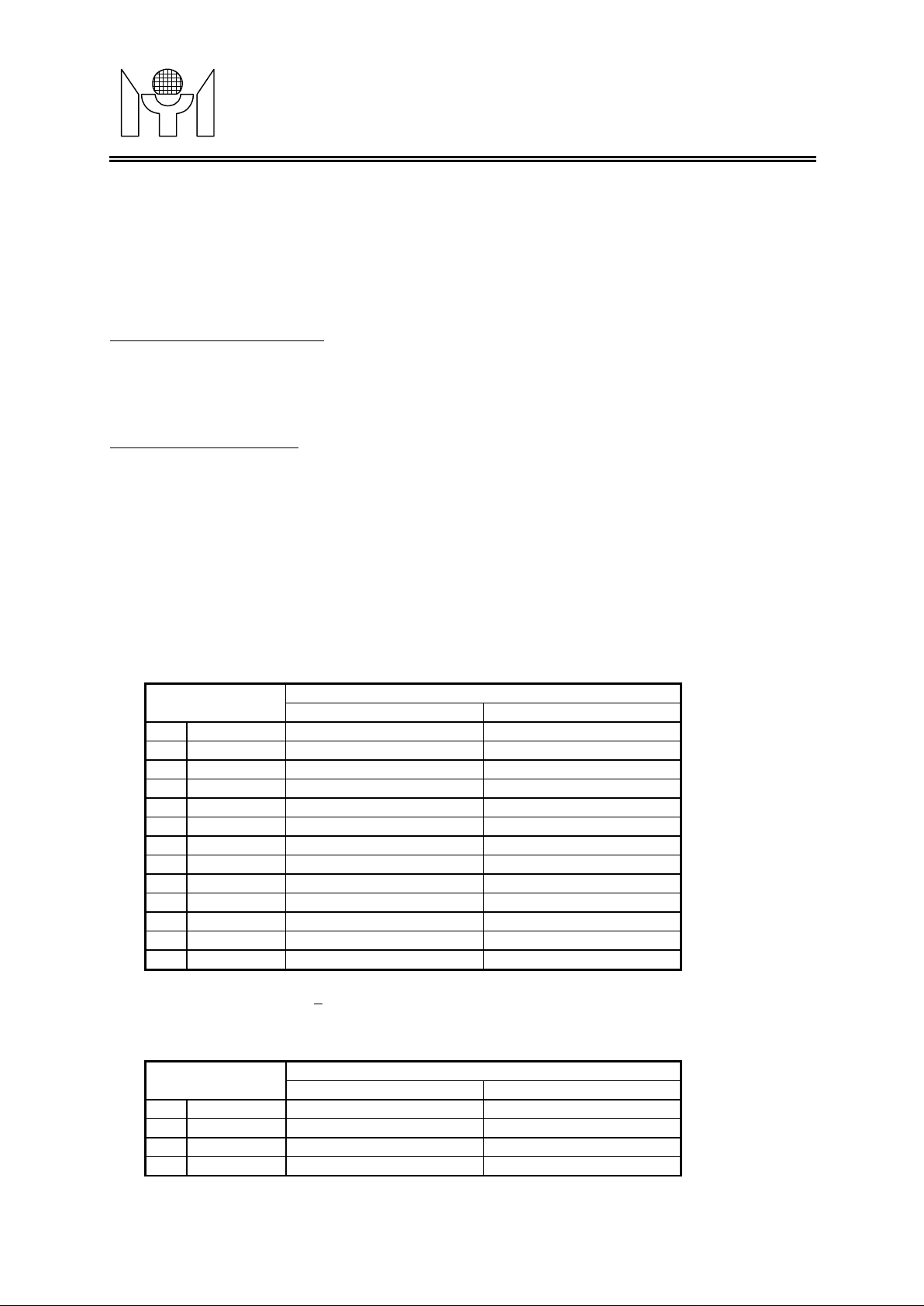
1.4 Ports2.4 ~ 2.7 are shared with DAC pins; ports3.0 ~ 3.2 and port3.4 are shared with monitor control
pins.
In addition, there are 2 timers, 5 interrupt sources and a serial interface compatible with the standard
8051. The Txd/Rxd (P3.0/P3.1) pins are shared with the DDC interface. INT0/T0 pins are shared with
the IIC interface. An extra option can be used to switch the INT0 source from P3.2 to P2.0. This feature
maintains an external interrupt source when the IIC interface is enabled.
Note: All regis t ers lis t ed in thi s doc u m ent resid e in the external RAM area (XFR). For the intern al
RAM memory map , please refer to th e 8051 spec.
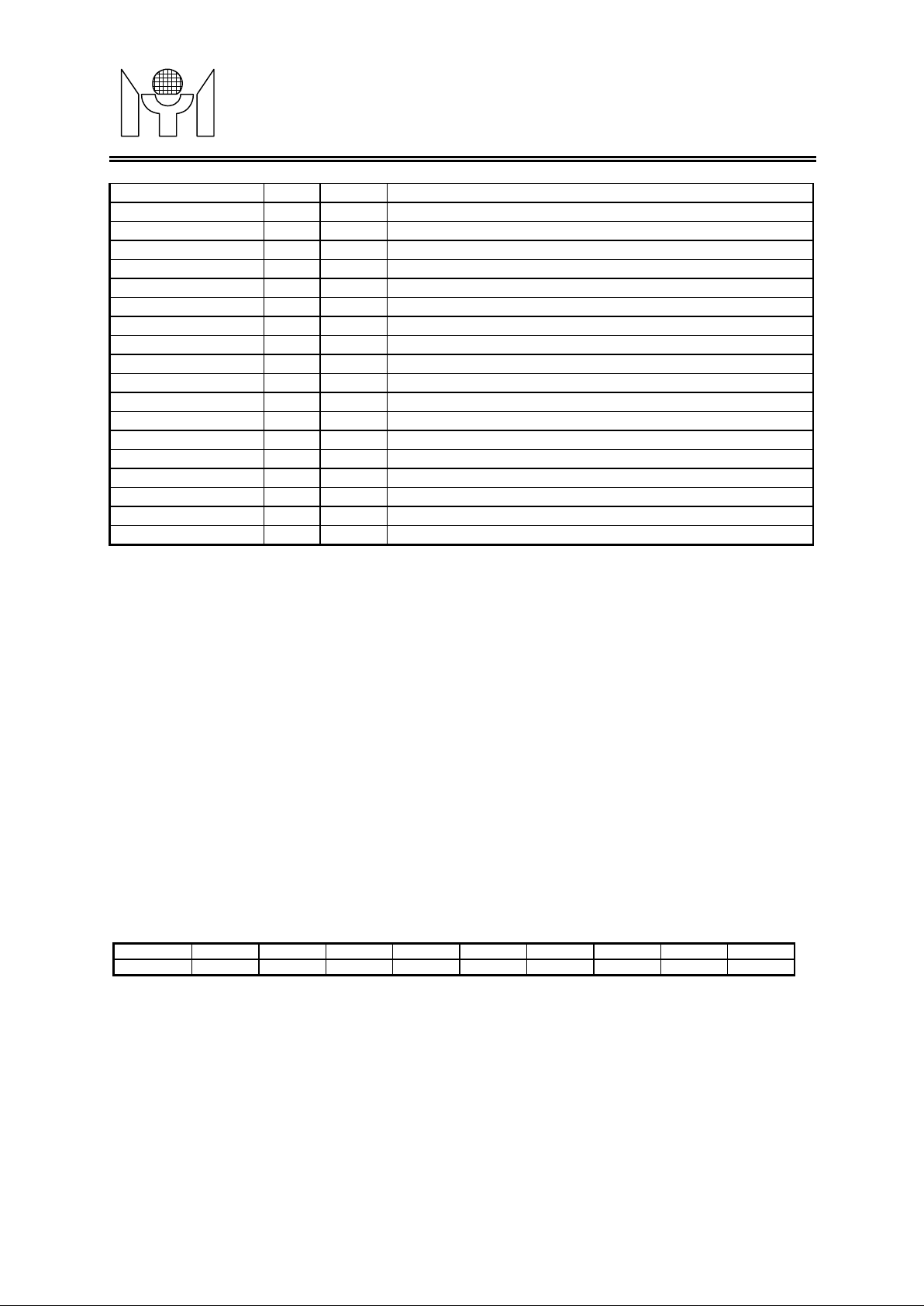
reg name addr bi t7 bit6 bit5 bit4 bit3 bit2 bit1 b it0
PADMOD
30h (w) SINT0 X DDCE IICE DA13E DA12E DA11E DA10E
SINT0 = 1 → INT0 source is pin #21.
= 0 → INT0 source is pin #12.
DDCE = 1 → Pin #10 is HSCL; pin #11 is HSDA.
= 0 → Pin #10 is P3.0/Rxd; pin #11 is P3.1/Txd.
IICE = 1 → Pin #12 is ISDA; pin #14 is ISCL.
= 0 → Pin #12 is P3.2/(INT0*); pin #14 is P3.4/T0.
DA13E = 1 → Pin #25 is DA13.
= 0 → Pin #25 is P2.4.
DA12E = 1 → Pin #26 is DA12.
= 0 → Pin #26 is P2.5.
3/14
MTV012E Revision 1.2 12/23/1998
Page 4

MYSON
MTV012E
TECHNOLOGY
DA11E = 1 → Pin #27 is DA11.
= 0 → Pin #27 is P2.6.
DA10E = 1 → Pin #28 is DA10.
= 0 → Pin #28 is P2.7.
* SINT0 should be 0 in this case.
2. External Special Func t i o n Regist ers (XFR)
The XFR is a group of registers allocated in the 8051 external RAM area. Most of the registers are used
for monitor control or PWM DAC. The program can initialize Ri value and use "MOVX" instruction to
access these registers.
3. PWM DAC
Each D/A converter's output pulse width is controlled by an 8-bit register in the XFR. The frequenc y of
these outputs is (Xtal frequency)/253 or (Xtal frequency)/256, selected by DIV253. If DIV253=1, writing
FDH/FEH/FFH to the DAC register generates a stable high output. If DIV253=0, the output will pulse low
at least once even if the DAC register's content is FFH. Writing 00H to the DAC register generates stable
low output.
reg name addr bi t7 bit6 b it5 bit4 bit3 b it2 bit1 bit0
DA0
DA1
DA2
DA3
DA4
DA5
DA6
DA7
DA8
DA9
DA10
DA11
DA12
DA13
WDT
20h (r/w) DA0
21h (r/w)
22h (r/w) DA2
23h (r/w)
24h (r/w) DA4
25h (r/w) DA5
26h (r/w) DA6
27h (r/w) DA7
28h (r/w)
29h (r/w) DA9
2Ah (r/w)
2Bh (r/w) DA11
2Ch (r/w) DA12
2Dh (r/w)
80h WEN WCLR CLRDDC DIV253 X WDT2 WDT1 WDT0
DA1
DA3
DA8
DA10
DA13
b7
b7
b7
b7
b7
b7
b7
b7
b7
b7
b7
b7
b7
b7
DA0
DA1
DA2
DA3
DA4
DA5
DA6
DA7
DA8
DA9
DA10
DA11
DA12
DA13
b6
b6
b6
b6
b6
b6
b6
b6
b6
b6
b6
b6
b6
b6
DA0
DA1
DA2
DA3
DA4
DA5
DA6
DA7
DA8
DA9
DA10
DA11
DA12
DA13
b5
b5
b5
b5
b5
b5
b5
b5
b5
b5
b5
b5
b5
b5
DA0
DA1
DA2
DA3
DA4
DA5
DA6
DA7
DA8
DA9
DA10
DA11
DA12
DA13
b4
b4
b4
b4
b4
b4
b4
b4
b4
b4
b4
b4
b4
b4
DA0
DA1
DA2
DA3
DA4
DA5
DA6
DA7
DA8
DA9
DA10
DA11
DA12
DA13
b3
b3
b3
b3
b3
b3
b3
b3
b3
b3
b3
b3
b3
b3
DA0
DA1
DA2
DA3
DA4
DA5
DA6
DA7
DA8
DA9
DA10
DA11
DA12
DA13
b2
b2
b2
b2
b2
b2
b2
b2
b2
b2
b2
b2
b2
b2
DA0
DA1
DA2
DA3
DA4
DA5
DA6
DA7
DA8
DA9
DA10
DA11
DA12
DA13
b1
b1
b1
b1
b1
b1
b1
b1
b1
b1
b1
b1
b1
b1
DA0 (r/w) : The output pulse width control for DA0.
DA1 (r/w) : The output pulse width control for DA1.
DA2 (r/w) : The output pulse width control for DA2.
DA3 (r/w) : The output pulse width control for DA3.
DA4 (r/w) : The output pulse width control for DA4.
DA5 (r/w) : The output pulse width control for DA5.
DA6 (r/w) : The output pulse width control for DA6.
DA7 (r/w) : The output pulse width control for DA7.
DA8 (r/w) : The output pulse width control for DA8.
DA9 (r/w) : The output pulse width control for DA9.
DA10 (r/w) : The output pulse width contro l f or DA10.
DA11 (r/w) : The output pulse width contro l f or DA11.
DA12 (r/w) : The output pulse width contro l f or DA12.
DA13 (r/w) : The output pulse width control for DA13.
WDT (w) : Watchdog timer & special control bit.
DIV253 = 1 → The PWM DAC output frequency is (Xtal frequency)/253.
= 0 → The PWM DAC output frequency is (Xtal frequency)/256.
*1. All D/A converters are centered with value 80h after power-on.
DA0
DA1
DA2
DA3
DA4
DA5
DA6
DA7
DA8
DA9
DA10
DA11
DA12
DA13
b0
b0
b0
b0
b0
b0
b0
b0
b0
b0
b0
b0
b0
b0
4/14
MTV012E Revision 1.2 12/23/1998
Page 5
MYSON
MTV012E
TECHNOLOGY
4. H/V SYNC Proces sing
The H/V SYNC processing block performs the functions of composite signal separation , SYNC input
presence check, frequency counting, and polarity detection and control, as well as protection of
VBLANK output while VSYNC speeds up to a high DDC comm unication clock rate. The present and
frequency function block treat any pulse shorter than 1 OSC period as noise.
4.1 Composite SYNC Separate
MTV012E continuously monitors the input HSYNC. If the vertical SYNC pulse can be extracted from the
input, a CVpre flag is set and the user can select the extracted "CVSYNC" for the source of polarity
check, frequency count and VBLANK. The CVSYNC will have a 10-16 us delay compared to the original
signal. The delay depends on the OSC frequency and composite m ix method.
4.2 H/V Frequency Counter
MTV012E can discriminate between HSYNC/VSYNC frequency and saves the information in XFRs. The
15-bit H counter counts the time of the 64xHSYNC period, but only 11 upper bits are loade d into the
HCNTH/HCNTL latch. The 11-bit output value will be (2/Hfreq) / (1/OSCfreq), updated once per
VSYNC/CVSYNC period when VSYNC/CVSYNC is present, or continuously updated when
VSYNC/CVSYNC is not present. The 14-bit V counter counts the tim e between 2 VSYNC pulses, but
only 9 upper bits are loaded into the VCNTH/VCNTL latch. The 9-bit output value will be (1/Vfreq) /
(512/OSCfreq), updated every VSYNC/CVSYNC period. An extra overflow bit indicates the condition of
H/V counter overflow. The VFchg/HFchg interrupt is active when VCNT/HCNT value changes or
overflows. Tables 4.2.1 and 4.2.2 show the HCNT/VCNT value under the 8MHz/12MHz OSC
operations.
4.2.1 H-Freq Table
H-Freq(KHZ)
1
2
3
4
5
6
7
8
9
10
11
12
13
*1. The H-Freq output (HF10 - HF0) is valid.
*2. The tolerance deviation is + 1 LSB.
4.2.2 V-Freq Table
V-Freq(Hz)
1
2
3
4
30 215h / 533 320h / 800
31.5 1FBh / 507 2F9h / 761
33.5 1DDh /477 2CCh / 716
35.5 1C2h / 450 2A4h / 676
36.8 1B2h / 434 28Ch / 652
38 1A5h / 421 277h / 631
40 190h / 400 258h / 600
48 14Dh / 333 1F4h / 500
50 140h / 320 1E0h / 480
57 118h / 280 1A5h / 421
60 10Ah / 266 190h / 400
64 0FAh / 250 177h / 375
100 0A0h / 160 0F0h / 240
56.25 115h / 277 1A0h / 416
59.94 104h / 260 187h / 391
60 104h / 260 186h / 390
60.32 103h / 259 184h / 388
8MHz OSC (hex / dec) 12MHz OSC (hex / dec)
8MHz OSC (hex / dec) 12MHz OSC (hex / dec)
Outpu t Value (11 bit s )
Outpu t Value (9 bits)
5/14
MTV012E Revision 1.2 12/23/1998
Page 6
MYSON
TECHNOLOGY
MTV012E
5
6
7
8
9
10
11
12
*1. The V-Freq output (VF8 - VF0) is valid.
*2. The tolerance deviation is + 1 LSB.
4.3 H/V Present Check
The H present function checks the input HSYNC pulse; the Hpre flag is set when HSYNC is over 10KHz
or cleared when HSYNC is under 10Hz. The V present function checks the input VSYNC pulse; the Vpre
flag is set when VSYNC is over 40Hz or cleared when VSYNC is under 10H z. The control bit "PREFS"
selects the time base for these functions. The HPRchg interrupt is set when the Hpre value changes.
The VPRchg interrupt is set when the Vpre/CVpre values change. However, the CVpre flag interrupt
may be disabled when S/W disables the composite function.
4.4 H/V Polarity Detection
The polarity functions detect the input HSYNC/VSYNC high and low pulse duty cycle. If the high pulse
duration is longer than that of the low pulse, the negative polarity is asserted; otherwise, positive polarity
is asserted. The HPLchg interrupt is set when the Hpol value changes. The VPLchg interrupt is set when
the Vpol value changes.
60.53 102h / 258 183h / 387
66.67 0EAh / 234 15Fh / 351
70.069 0DEh / 222 14Eh / 334
70.08 0DEh / 222 14Eh / 334
72 0D9h /217 145h / 325
72.378 0D7h / 215 143h / 323
72.7 0D6h / 214 142h / 322
87 0B3h / 179 10Dh / 269
4.5 Output HBLANK/VBLANK Control and Polarity Adjustment
HBLANK is the MUX output of HSYNC and the self-test horizontal pattern. The VBL ANK is the MUX
output of VSYNC, CVSYNC and the self-test vertical pattern. The MUX selection and output polarity are
S/W controllable. The VBLANK output is cut off when VSYNC frequency is over 200Hz or 133Hz
depends on 8MHz/12MHz OSC selection. HBLANK/VBLANK shares the output pin with P4.1/ P4.0.
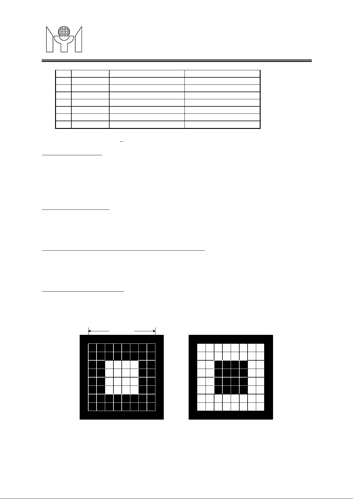
4.6 Self-Test Pattern Generator
This generator can generate 4 display patterns for testing purposes: positive cross-hatch, negative
cross-hatch, full white and full black (shown in the following figure). It was originally designed to support
monitor manufacturers to do a burn-in test, or offer the end-user a reference to check the monitor. The
generator's output STOUT shares the output pin with P4.2.
Display Region
Self-Test Patterns (1)
6/14
MTV012E Revision 1.2 12/23/1998
Page 7
MYSON
TECHNOLOGY
4.7 H/V Sync Processor Register
MTV012E
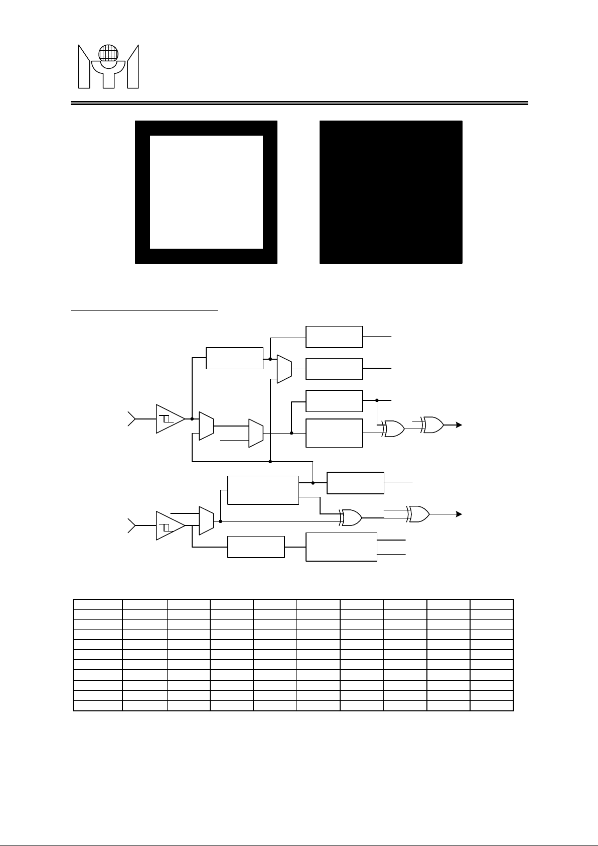
Self-Test Patterns (2)
VSYNC
Hself
Digital Filter
Vself
CVSYNC
Polarity Check &
Sync Seperator
Present
Check
Frequency
Count
Polarity
Check
High
Frequency
Mask
Hpol
Present
Check
Vpre
Vfreq
Vpol
VBpl
VBLANK
CVpre
HBpl
HBLANK
HSYNC
Hpre
Hfreq
Digital Filter
Present Check &
Frequency Count
H/V SYNC Processor Block Diagram
reg name addr bit7 bi t6 bit5 b it4 bit3 bit2 b it1 bit0
PSTUS
HCNTH
HCNTL
VCNTH
VCNTL
PCTR0
PCTR2
P4OUT
INTFLG
INTEN
40h (r) CVpre X Hpol Vpol Hpre Vpre Hoff Voff
41h (r) Hovf X X X X HF10 HF9 HF8
42h (r) HF7 HF6 HF5 HF4 HF3 HF2 HF1 HF0
43h (r) Vovf X X X X X X VF8
44h (r) VF7 VF6 VF5 VF4 VF3 VF2 VF1 VF0
40h (w) C1 C0 HVsel STOsel PREFS HALFV HBpl VBpl
42h (w) X X X Selft ST
44h (w) X X X X X P42 P41 P40
50h (r/w) HPRchg VPRchg HPLchg VPLchg HFchg VFchg FIFOI MI
60h (w) EHPR EVPR EHPL EVPL EHF EVF EFIFO EMI
bsh
Rt1 Rt0 STF
PSTUS (r): The status of polarity, present and static level for HSYNC and VSYNC.
CVpre = 1 → The extracted CVSYNC is present.
= 0 → The extracted CVSYNC is not present.
H
= 1 → HSYNC input is positive polarity.
pol
MTV012E Revision 1.2 12/23/1998
7/14
Page 8

MYSON
TECHNOLOGY
= 0 → HSYNC input is negative po lari ty.
V
H
V
H
V
*H
HCNTH (r) : H-Freq counter's high bits.
Hovf = 1 → H-Freq counter overflows; this bit is cleared by H/W when condition
HF10 - HF8 : 3 high bits of H-Freq counter.
HCNTL (r) : H-Freq counter's low bits.
= 1 → VSYNC (CVSYNC) is positive polarity.
pol
= 0 → VSYNC (CVSYNC) is negat ive polarity.
= 1 → HSYNC input is present.
pre
= 0 → HSYNC input is not present.
= 1 → VSYNC input is present.
pre
= 0 → VSYNC input is not present.
= 1 → HSYNC input's off-level is high.
off*
= 0 → HSYNC input's off-level is low.
= 1 → VSYNC input's off-level is high.
off*
= 0 → VSYNC input's off-level is low.
off
and V
are valid when H
off
removed.
pre=0
or V
MTV012E
pre=0.
VCNTH (r) : V-Freq counter's high bits.
Vovf = 1 → V-Freq counter overflows; this bit is cleared by H/W when condition
removed.
VF8 : High bit of V-Freq counter.
VCNTL (r) : V-Freq counter's low bits.
PCTR0 (w) : SYNC processor control register 0.
C1, C0 = 1,1 → Selects CVSYNC as the polarity, freq and VBLANK source.
= 1,0 → Selects VSYNC as the polarity, freq and VBLANK source.
= 0,0 → Disables composite function (MTV012 compatible mode).
= 0,1 → H/W auto switch to CVSYNC when CVpre =1 and VSpre=0.
HVsel = 1 → Pin #16 is P41, pin #17 is P40.
= 0 → Pin #16 is HBLANK, pin #17 is VBLANK.
STOsel = 1 → Pin #29 is P42.
= 0 → Pin #29 is STOUT.
PREFS = 0 → Selects 8MHz OSC as H/V present check and self-test pattern time base.
= 1 → Selects 12MHz OSC as H/V present check and self-test pattern time base.
HALFV = 1 → VBLANK is half frequency output of VSYNC.
HB
VB
PCTR2 (w) : Self-test pattern generator control.
S
ST
Rt1,Rt0 = 0,0 → Positive cross-hatch pattern output.
= 1 → Negative polarit y HBLANK output.
pl
= 0 → Positive polarity HBLANK ou tput .
= 1 → Negative polarity VBLANK output.
pl
= 0 → Positive polarity VBLANK output.
= 1 → Enables generator.
elft
= 0 → Disables generator.
= 1 → 63.5KHz (horizontal) output selected.
bsh
= 0 → 31.75KHz (horizontal) output selected.
= 0,1 → Negative cross-hatch pattern output.
= 1,0 → Full white pattern output.
= 1,1 → Full black pattern output.
8/14
MTV012E Revision 1.2 12/23/1998
Page 9

MYSON
MTV012E
TECHNOLOGY
STF = 1 → Enables STOUT output.
= 0 → Disables STOUT output.
P4OUT (w) : Port 4 data output value.
INTFLG (w) : Interrupt flag. An interrupt event will set its individual flag, and, if the corresponding
interrupt enable bit is set, the 8051 core's INT1 source will be driven by a zero level.
Software MUST clear this register while serving the interrupt routine.
HPRchg= 1 → No action.
= 0 → Clears HSYNC presence change flag.
VPRchg= 1 → No action.
= 0 → Clears VSYNC presence change flag.
HPLchg= 1 → No action.
= 0 → Clears HSYNC polarity change flag.
VPLchg= 1 → No action.
= 0 → Clears VSYNC polarity change flag.
HFchg = 1 → No action.
= 0 → Clears HSYNC frequency change f lag.
VFchg = 1 → No action.
= 0 → Clears VSYNC frequency change flag.
INTFLG (r) : Interrupt flag.
HPRchg= 1 → Indicates an HSYNC presence change.
VPRchg= 1 → Indicates a VSYNC presence change.
HPLchg= 1 → Indicates an HSYNC polarity change.
VPLchg= 1 → Indicates a VSYNC polarity change.
HFchg = 1 → Indicates an HSYNC frequency change or counter overflow.
VFchg = 1 → Indicates a VSYNC frequency change or counter overflow.
INTEN (w) : Interrupt enabler.
EHPR = 1 → Enables HSYNC presence change interrupt.
EVPR = 1 → Enables VSYNC presence change interrupt.
EHPL = 1 → Enables HSYNC polarity change interrupt.
EVPL = 1 → Enables VSYNC polarity change interrupt.
EHF = 1 → Enables HSYNC frequency change / counter overflow interrupt.
EVF = 1 → Enables VSYNC frequency change / counter overflow interrupt.
5. DDC & IIC Int erface
5.1 DDC1 Mode
MTV012E enters DDC1 mode after Reset. In this mode, VSYNC is used as a data clock. The HSCL pin
should remain at high. The data output to the HSDA pin is taken from 8 bytes of FIFO in MTV012E.
MTV012E fetches the data byte from FIFO, then sends it in a 9-bit packet format which includes a null bit
(=1) as packet separator. The software program should load EDID data (original stored in EEPROM)
into FIFO and take care of the FIFO depth. FIFO sets the FIFOI (FIFO low interrupt) flag when there are
fewer than N (N=2,3,4 or 5 controlled by LS1, LS0) bytes to be output to the HSDA pin. To prevent FIFO
from emptying, software needs to write EDID data to FIFO as soon as FIFOI is set. On t he o ther hand,
FIFO sets the FIFOH flag when its capacity is full. Software should not write additional data to FIFO in
such an instance. The FIFOI interrupt can be masked or enabled by an EFIFO control bit. A simple way
to control FIFO is to set (LS1, LS0=1,0) and enable FIFOI interrupt, then software may load 4 bytes into
FIFO each time a FIFOI interrupt arises. A special control bit "LDFIFO" can reduce the software effort
when EDID data is stored in EEPROM. If LDFIFO=1, FIFO will be automatically loaded with MBUF data
when software reads MBUF XFR.
9/14
MTV012E Revision 1.2 12/23/1998
Page 10

MYSON
MTV012E
TECHNOLOGY
5.2 DDC2B Mode
MTV012E switches to DDC2B mode when it detects a high to low transition on the HSCL pin. Once
MTV012E enters DDC2B mode, the host can access the EEPROM using IIC bus protocol as if the
HSDA and HSCL are directly bypassed to ISDA and ISCL pins. MTV012E will return to DDC1 mode if
HSCL is kept high for a 128-VSYNC clock period. However, it will 100K in DDC2B mode if a valid IIC
access has been detected on the HSCL/HSDA bus. The DDC2 flag reflects the current DDC status; S/W
may clear it by setting CLRDDC. The control bits M128/M256 are used to block the EEPROM write
operation from the host if the address is over 128/256.
5.3 Master Mode IIC Function Block
The master mode IIC block is connected to the ISDA and ISCL pins. The software program can access
the external EEPROM through this interface. Since the EDID/VDIF data and the display information
share the common EEPROM, precaution must be taken to avoid bus conf lict. In DDC1 mode, the IIC
interface is controlled by MTV012E only. In DDC2B mode, the host may access the EEPROM directly.
Software can test the HSCL condition by reading the BUSY flag, which is set in case of HSCL=0. A
summary of master IIC access is illustrated as follows:
5.3.1. To Write EEPROM
1. Write to MBUF the EEPROM slave address (bit 0 = 0).
2. Set S bit to Start.
3. After MTV012E transmits this byte, a MI interrupt will be triggered.
4. The program can write MBUF to transfer the next byte, or set the P bit to stop.
* Please see the attachments about "Master IIC Transmission Timing".
5.3.2. To Read EEPROM
1. Write to MBUF the slave address (bit 0 = 1).
2. Set the S bit to Start.
3. After MTV012E transmits this byte, a MI interrupt will be triggered.
4. Set or reset the ACK flag according to the IIC protocol.
5. Read out to MBUF the useless byte in order to continue the data transfer.
6. After MTV012E receives a new byte, the MI interrupt is triggered again.
7. Reading MBUF also triggers the next receiving operation, but the P bit needs to be set before reading
can terminate the operation.
* Please see the attachments about the "Master IIC Timing Receiving".
5.4 Slave Mode IIC Function Block
The slave mode IIC block can be connected to HSDA/HSCL pins or ISDA/ISCL pins, and selected by the
SLVsel control bit. This block is receiving mode only. S/W may set the SLVADR register to determine the
address range to which this block should respond. The block first detects an IIC slave address match
condition, then issues a SLVMI interrupt. The data received from SDA is shifted onto the shift register
and moved to the SLVBUF latch. The first byte loaded is the word address (the slave address is
dropped). This block also generates a SLVBI each time the SLVBUF is loaded. If S/W can't read out the
SLVBUF in time, the next byte will not be written to SLVBUF and the slave block returns NACK to the
master. This feature guarantees the data integrity of communication. A WADR flag can tell S/W if the
data in SLVBUF is a word address.
* Please see the attachments about "Slave IIC Block Timing".
6. Low Power Reset (LVR) & Watch d o g Tim er
When the voltage level of the power supply is below 4.0V for a specific time, the LVR will generate a chip
reset signal. After the power supply is above 4.0V, LVR maintains the reset state for a 144 Xtal cycle to
guarantee that the chip exit reset condition has a stable Xtal oscillation. The specific time of power
supply in the low level is 3us and is adjustable by an external capacitor connected to the RST pin.
The watchdog timer automatically generates a device reset when it overflows. The interval of overflow is
0.25 sec x N, in which N is a number from 1 to 8, and can be programmed via register WDT(2:0). The
MTV012E Revision 1.2 12/23/1998
10/14
Page 11
MYSON
WADR
MTV012E
TECHNOLOGY
timer function is disabled after power-on reset; the user can activate this function by setting WEN, and
clear the timer by setting WCLR.
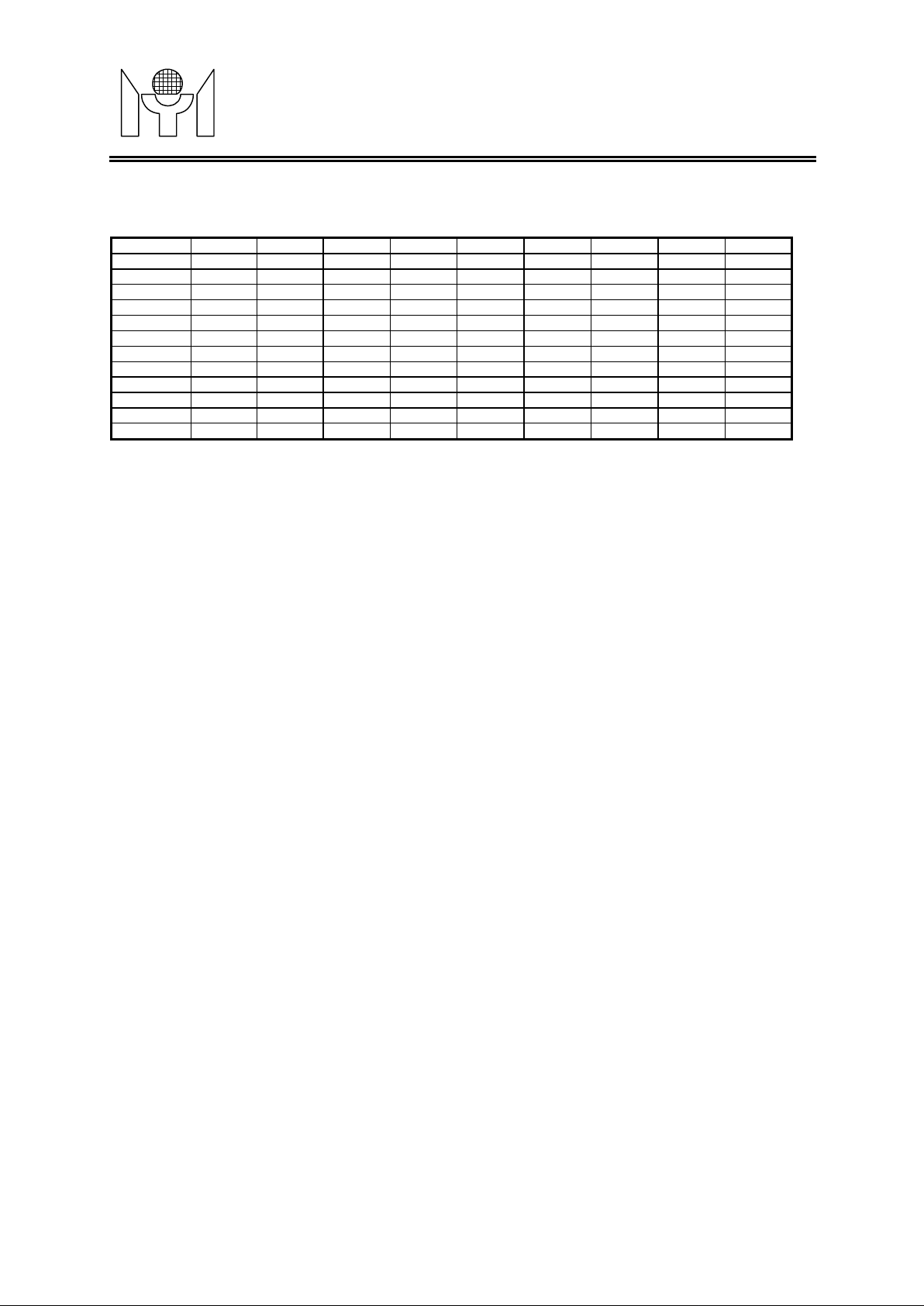
reg name addr bit7 bit6 bit5 bit4 b it3 bit2 bit1 b it0
MSTUS
MBUF
INTFLG
MCTR
INTEN
FIFO
WDT
SLVCTR
SLVSTUS
SLVINT
SLVBUF
SLVADR
MCTR (w) : Master IIC interface control register.
* MTV012E uses a 100KHz clock to sample the S/P bit; any pulse should sustain at least 20us.
* A write/read MBUF operation can be recognized only after 10us of the MI flag's rising edg e.
00h (r) X SCLERR DDC2 BERR HFREQ FIFOH FIFOL BUSY
10h (r/w) MBUF7 MBUF6 MBUF5 MBUF4 MBUF3 MBUF2 MBUF1 MBUF0
50h (r/w) HPRchg VPRchg HPLchg VPLchg HFchg VFchg FIFOI MI
00h (w) LS1 LS0 LDFIFO M256 M128 ACK P S
60h (w) EHPR EVPR EHPL EVPL EHF EVF EFIFO EMI
70h (w) FIFO7 FIFO6 FIFO5 FIFO4 FIFO3 FIFO2 FIFO1 FIFO0
80h (w) WEN WCLR CLRDDC DIV253 LVSEL WDT2 WDT1 WDT0
90h (w) ENSLV SLVsel ESLVBI ESLVMI X X X X
91h (r)
91h (w) X X X SLVMI X X X X
92h (r) SLVbuf7 SLVbuf6 SLVbuf5 SLVbuf4 SLVbuf3 SLVbuf2 SLVbuf1 SLVbuf0
93h (w) SLVadr7 SLVadr6 SLVadr5 SLVadr4 SLVadr3 SLVadr2 SLVadr1 X
SLVS SLVBI SLVMI X X X X
LS1, LS0 = 11 → FIFOL is the status which has a FIFO depth of < 5.
= 10 → FIFOL is the status which has a FIFO depth of < 4.
= 01 → FIFOL is the status which has a FIFO depth of < 3.
= 00 → FIFOL is the status which has a FIFO depth of < 2.
LDFIFO = 1 → FIFO will be written while S/W reads MBUF.
M256 = 1 → Disables host writing EEPROM when address is over 256.
M128 = 1 → Disables host writing EEPROM when address is over 128.
ACK = 1 → In receiving mode, there is no acknowledgment by MTV012E.
= 0 → In receiving mode, ACK is returned by MTV012E.
S, P = ↑,0 → Start condition when Master IIC is not transferring.
= X,↑ → Stop condition when Master IIC is not transferring.
= 1,X → Will resume transfer after a read/write MBUF operation.
= X,0 → Forces HSCL low and occupies the IIC bus.
MSTUS (r) : Master IIC interface status register.
SCLERR = 1 → The ISCL pin is pulled-low by other devices during the
transfer, and cleared when S=0.
DDC2 = 1 → DDC2B is active.
= 0 → MTV012E remains in DDC1 mode.
BERR = 1 → IIC bus error, no ACK received from the slave, updated every time
when slave sends ACK on the ISDA pin.
HFREQ = 1 → MTV012E detects a higher than 200Hz clock on the VSYNC pin.
FIFOH = 1 → FIFO high indicated.
FIFOL = 1 → FIFO low indicated.
BUSY = 1 → Host drives the HSCL pin to low.
* While writing FIFO, the FIFOH/FIFOL flag will reflect the FIFO condition after 30us.
INTFLG (w) : Interrupt flag. An interrupt event will set its individual flag and, if the corresponding
interrupt enable bit is set, the 8051 INT1 source will be driven b y a zero level. Software
MUST clear this register while serving the interrupt routine.
FIFOI = 1 → No action.
= 0 → Clears FIFOI flag.
MI = 1 → No action.
= 0 → Clears Master IIC bus interrupt flag (MI).
MTV012E Revision 1.2 12/23/1998
11/14
Page 12

MYSON
MTV012E
TECHNOLOGY
INTFLG (r) : Interrupt flag.
FIFOI = 1 → Indicates the FIFO low condition; when EFIFO is set, MTV012E will be
interrupted by INT1.
MI = 1 → Indicates when a byte is sent/received to/from the IIC bus; when EMI is
active, MTV012E will be interrupted by INT1.
INTEN (w) : Interrupt enabler.
EFIFO = 1 → Enables FIFO interrupt.
EMI = 1 → Enables master IIC bus interrupt.
MBUF (w) : Master IIC data shift register write; after START and before STOP condition, this
register will resume MTV012E's transmission to the IIC bus.
MBUF (r) : Master IIC data shift register read; after START and before STOP condition, this
register will resume MTV012E's receiving from the IIC bus.
WDT (w) : Watchdog timer control register.
WEN = 1 → Enables the watchdog timer.
WCLR = 1 → Clears the watchdog timer.
CLRDDC = 1 → Clears the DDC2 flag.
WDT2: WDT0 = 0 → Overflow interval = 8 x 0.25 sec.
= 1 → Overflow interval = 1 x 0.25 sec.
= 2 → Overflow interval = 2 x 0.25 sec.
= 3 → Overflow interval = 3 x 0.25 sec.
= 4 → Overflow interval = 4 x 0.25 sec.
= 5 → Overflow interval = 5 x 0.25 sec.
= 6 → Overflow interval = 6 x 0.25 sec.
= 7 → Overflow interval = 7 x 0.25 sec.
FIFO (w) : Writes FIFO contents.
SLVCTR (w) : Slave IIC block control.
ENSLV = 1 → Enables slave IIC block.
= 0 → Disables slave IIC block.
SLVsel = 1 → Slave IIC connects to ISD A/ISCL.
= 0 → Slave IIC connects to HSDA/HSCL.
ESLVBI = 1 → Enables slave buffer interrupt.
ESLVMI = 1 → Enables slave address match interrupt.
SLVSTUS (r) : Slave IIC block status.
WADR = 1 → The data in SLVBUF is a word address.
SLVS = 1 → The slave block has detected a START; will be cleared when STOP
is detected.
SLVBI = 1 → SLVBUF has been loaded with a new data byte; reset by S/W
reading SLVBUF.
SLVMI = 1 → Slave block has detected the slave address match condition; cleared
by S/W writing 0 to SLVMI.
SLVINT (w) : Slave block interrupt. The SLVBI/SLVMI interrupt will set its flag, and, if the
corresponding interrupt enable bit is set, the 8051 INT1 source will be driven by a zero
level. Software MUST clear this register while serving the interrupt routine.
SLVMI = 1 → No action.
= 0 → Clears SLVMI.
SLVBUF (r) : Slave IIC data latch.
MTV012E Revision 1.2 12/23/1998
12/14
Page 13
MYSON
MTV012E
TECHNOLOGY
SLVADR (w) : Slave IIC address to which the slave block should respond.
4.0 Test Mode Condit io n
In normal application, users should not allow MTV012E to enter its test/program mode, outlined as
follows:
Test Mode A: RESET=1 & DA9=1 & DA8=0 & STO=0
Test Mode B: RESET falling edge & DA9=1 & DA8=0 & STO=1
Program Mode: RESET=1 & DA9=0 & DA8=1
5.0 INTERNAL EPROM
To program the internal EPROM, MTV012E must be running at a 4 to 6 MHz cycle time. The address of
an EPROM location to be programmed is applied to Port1 (A0 - A7) and pins P2.0 - P2.4(A8 - A12) of
Port2, while the code byte to be programmed is applied to DA0 - DA7. All other pins should be held at the
level indicated in the following table. The overall programming characteristics are very similar to those of
87C52 with the exception that pin #30 and pin #31 are switched.
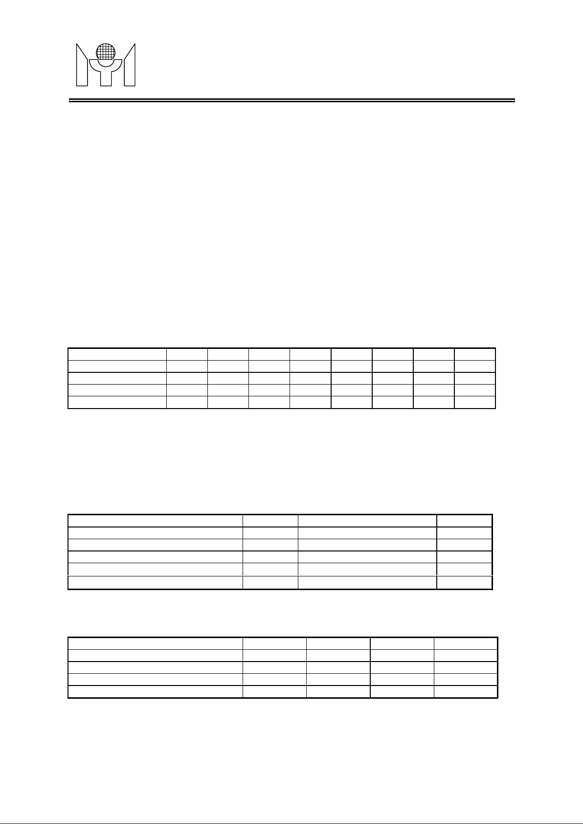
Mode
Normal Reset
Progr am Code Data
Program Lock Bit
Verify Code
Note 1: VPP = 12.7V
Note 2: P* is pulsed low for 100uS for programming.
RST DA9 STOUT DA8 P2.7 P2.6 HBL ANK VBL ANK
1 1 0 1 X X X X
1 0 P* VPP 1 0 1 1
1 0 P* VPP 1 1 1 1
1 0 1 1 0 0 1 1
6.0 ELECTRICAL PARAMETERS
6.1 Absolu te Maximum Ratings
at: Ta= 0 to 70 oC, VSS=0V
Name Symbol Range Unit
Maximum Supply Voltage VDD -0.3 to +6.0 V
Maximum Input Voltage Vin -0.3 to VDD+0.3 V
Maximum Output Voltage Vout -0.3 to VDD+0.3 V
Maximum Operating Temperature Topg 0 to +70
Maximum Storage Temperature Tstg -25 to +125
6.2 Allowable Operating Condit io n s
at: Ta= 0 to 70 oC, VSS=0V
Name Symbol Min. Max. Unit
Supply Voltage VDD 4.0 6.0 V
Input "H" Voltage Vih1 0.7 x VDD VDD +0.3 V
Input "L" Voltage Vil1 -0.3 0.15 x VDD V
Operating Freq. Fopg - 15 MHz
o
C
o
C
13/14
MTV012E Revision 1.2 12/23/1998
Page 14
MYSON
tVIPW
tVIPW
tVCPW
tVCPW
MTV012E
TECHNOLOGY
6.3 DC Characteri s t i c s
at: Ta=0 to 70 oC, VDD=4.0V ~ 6.0V, VSS=0V
Name Symbol Condition Min. Typ. Max. Unit
Output "H" Voltage, except opendrain pins, pins #16, 17, 29
Output "H" Voltage, pins #16, 17, 29 Voh2 Ioh=-1mA 4 V
Output "L" Voltage Vol Iol=8mA 0.45 V
Power Supply Current Idd
RST Pull-Down Resistor Rrst VDD=5V 50 150 Kohm
Pin Capacitance Cio 15 pF
6.4 AC Characterist ic s
at: Ta=0 to 70 oC, VDD=4.0V ~ 6.0V, VSS=0V
Name Symbol Condition Min. Typ. Max. Unit
Crystal Frequency fXtal 8 MHz
PWM DAC Frequency fDA fXtal=8MHz 31.25 31.62 KHz
PWM DAC Frequency fDA fXtal=12MHz 46.875 47.43 KHz
HS Input Pulse Width tHIPW fXtal=8MHz 0.3 12 uS
VS Input Pulse Width
HS Input Pulse Width tHIPW fXtal=12MHz 0.2 8 US
VS Input Pulse Width
HSYNC to HBLANK Output Jitter tHHBJ 5 NS
H+V to VBLANK Output Delay tVVBD fXtal=8MHz 16 uS
H+V to VBLANK Output Delay tVVBD fXtal=12MHz 10 uS
VS Pulse Width in H+V Signal
VS Pulse Width in H+V Signal
Voh1 Ioh=-50uA 4 V
Active 18 24 mA
Idle 1.3 4.0 mA
Power-Down 50 80 uA
fXtal=8MHz 3 US
fXtal=12MHz 2 US
fXtal=8MHz 32 uS
fXtal=12MHz 20 uS
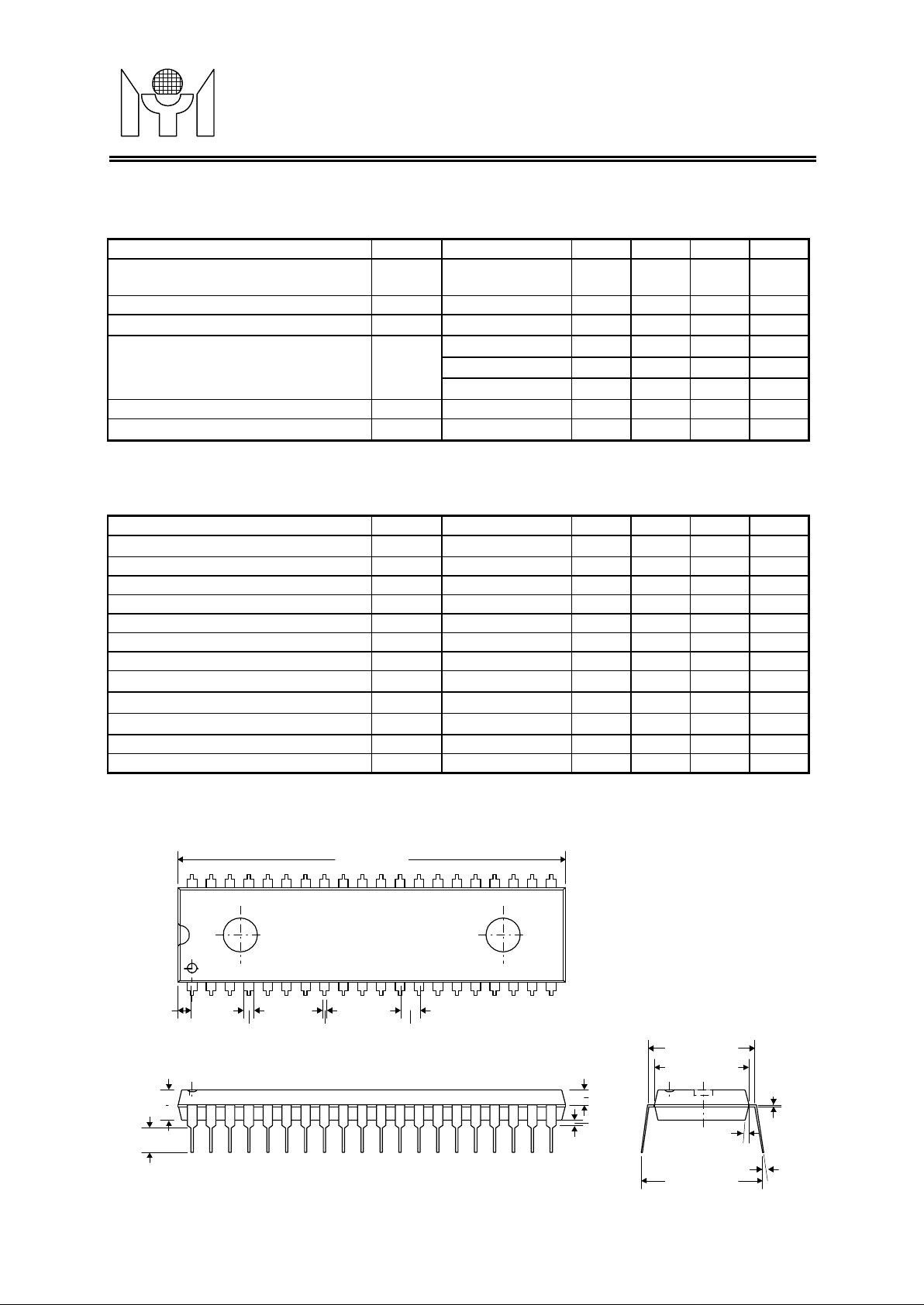
6.0 PACKAGE DIMENSION
40 PIN PDIP 600 mil
1.981mm
+/-0.254
3.81mm
+/-0.127
3.302mm
+/-0.254
52.197mm +/-0.127
MTV 012
2.540mm0.457mm +/-0.1271.270mm +/-0.254
14/14
15.494mm +/-0.254
13.868mm +/-0.102
1.778mm
+/-0.127
0.254mm
(min.)
16.256mm +/-0.508
MTV012E Revision 1.2 12/23/1998
5o~7
0
6o +/-3
0.254mm
o
+/-0.102
 Loading...