

Page 1
MYSON
Operating voltage: 2.4v ~ 6.0v
1 trigger input PAD
1 Level option input
1 status output (
_LED_slow; Dynamic)
Play times: max. 8 (Total 8)
Voice length: 3 seconds for MTS3103, 6 seconds for MTS3106 and 9 seconds for MTS3109
LOG_PCM
PWM1
PWM2
Clock
MTS3103/6/9
TECHNOLOGY
(Rev 2.1)
3, 6 and 9 Seconds Simple Pure Speech
FEATURES
•
• Single word
•
•
•
• Trigger mode selection: Edge/Level, Hold/Unhold, Retrigger/Irretrigger
• Debounce mode : Fast debounce: < 30us
• Slow debounce : ~10ms (S.R. = 6kHz)
•
• PWM playing port; Drive speaker or buzzer directly
•
(S.R. = 6kHz) (Rom capacity = 18048*5 bit for MTS3103/ 36096*5 bit for MTS3106
/ 54272*5 bit for MTS3109)
• Voice+Mute length : up to ~20 seconds. (S.R. = 6kHz)
• Voice algorithm : Log_PCM
• External resister for system frequency.
GENERAL DESCRIPTION
The MTS3103/6/9 is a single-chip synthesizing CMOS VLSI that can synthesize voice up to 3 seconds, 6
seconds and 9 seconds by Log_PCM algorithm.
Customers’ speech data are edited and programmed into ROM by changing one mask during the device
fabrication.
Busy_high; Static_LED_fast;Static
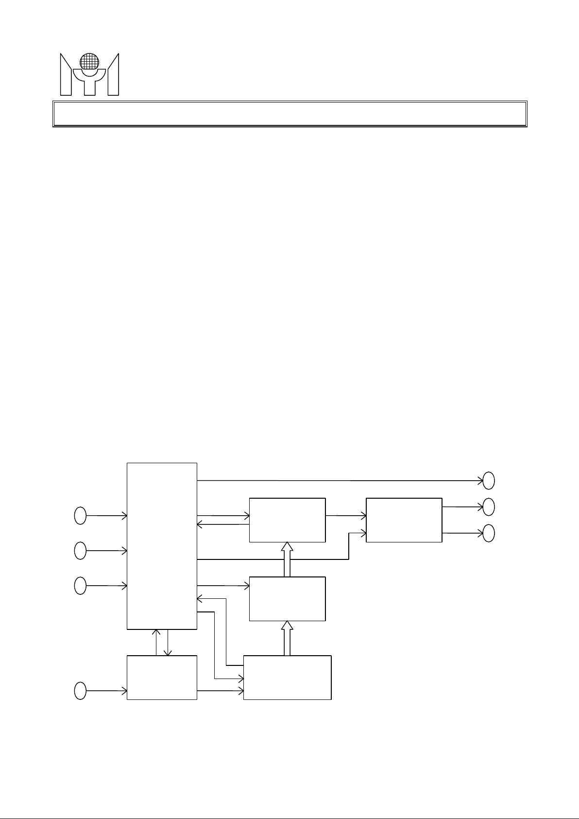
BL OCK DIAGRAM
TG
Control Logic
TEST
FL
Generator
OSC
OP
Decoder
ROM
Address generator
Output Buffer
This datasheet contains new product information. Myson Technology reserves the rights to modify the product specification without notice.
No liability is assumed as a result of the use of this product. No rights under any patent accompany the sale of the product.
Revision 2.1 - 1 - 2001/07/16
Page 2
MYSON
Attr.
Test enable pad, high active, pull low
2.0 AB SOLUTE MAXIMUM RATING
3.0 DC CHARACTERESTICS
Typ.
Operating Voltage
Standby
Vdd=3.0V, I/O open
Vdd=3.0v, No loading
Vdd=3.0v, Vip=0v
Vdd=3.0v, Vip=3.0v
Vdd=3.0v, Vop=0.8v
Vdd=3.0v, Vop=2.5v
Variation by Lot
MTS3103/6/9
TECHNOLOGY
1.0 PIN DESCRIPTION
Pin Name Pin
VDD Power Positive power supply
TG In Trigger input, active high, pull low; with CDS interface
FL In Force edge mode be level mode, internal pull low
TEST In
OP Out Status output
OSC In W ith resister connecting to VDD for system clock generating
PWM1 Out Voltage output to drive speaker or buzzer
PWM2 Out Voltage output to drive speaker or buzzer
VSS Power Negative power supply
SYMBOL RATING UNIT
VDD ~ VSS -0.5 ~ +7.0 V
VIN ( for input ) VSS – 0.3 < VIN < VDD + 0.3 V
VOUT ( for all outputs ) VSS < VOUT < VDD V
T ( operating ) -10 ~ +60 V
T ( storage ) -55 ~ +125 V
(Rev 2.1)
Descripti on
Symbol Parameter Min
VDD
Isb
Iop
Iih - - -20 uA
Iil
Iol - 8 - mA
Ioh
d F/F Frequency
d F/F Frequency
Supply
Current
Output Current
Operating - - 400 uA
Input Current
Stability
Max. Unit Condition
2.4 3.0 6.0 V
- - 1 uA
- - 20 uA
- -5 - mA
- -
- -
± 5
± 10
% Fosc(4.5v)-Fosc(4.0)
% Vdd=4.5V
Fosc(4.5v)
Fosc=384kHz
Revision 2.1 - 2 - 2001/07/16
Page 3
MYSON
Trigger length > Voice length
Trigger length < Voice length
( or edge mod e, FL PAD = HIGH )
MTS3103/6/9
TECHNOLOGY
4.0 FUNCTION DIAGRAM
4.1 Edge / Level mo d e (If play time=2)
Edge mode
TG
Audio
TG
Audio
(Rev 2.1)
word word
debounce time
word word
debounce time
Level mod e
Trigger length > Voice length (including repeat voice)
Trigger length < Voice length (including repeat voice)
4.2 Hold/Unho l d mo d e (If pl ay tim e=2)
Hold mode
TG
Audio
debounce time
TG
Audio word
word word word word
word
debounce time
TG
Audio
Revision 2.1 - 3 - 2001/07/16
word
debounce time
word
Page 4

MYSON
MTS3103/6/9
TECHNOLOGY
Unhold mode
TG
Audio
4.3 Retrigger/Irretrigger mode ( If pl ay t i me=2 )
Retrigg er mo d e (Edge, Unhold mod e)
TG
Audio
word word
debounce time
word word
debounce time
word
(Rev 2.1)
word
Irretrig g er mo d e (Edg e, Unhol d mod e)
TG
Audio
word word
debounce time
Revision 2.1 - 4 - 2001/07/16
Page 5

MYSON
5.0 APPLICATION CIRCUIT
5.1 External resi ster, Drive sp eaker, LED
PWM1
PWM2
PWM1
PWM2
MTS3103/6/9
TECHNOLOGY
Rosc
Rosc = 200k Ω
OSC
TG
VDD
MTS310x
VSS
(Rev 2.1)
OP
5.2 Int ern al opt io n is edge mode, by PAD option to Level mod e.
VDD
Rosc
OSC
TG
FL
MTS310x
VSS
OP
Revision 2.1 - 5 - 2001/07/16
Page 6

MYSON
PWM1
PWM2
PWM1
PWM2
MTS3103/6/9
TECHNOLOGY
5.3 Power on pl ay
Rosc
OSC
TG
VDD
MTS310x
VSS
(Rev 2.1)
OP
6.0 BONDING DIAGRAM
Y
VSS
(1) MTS3103
PIN NAME X(µm) Y(µm)
P AD_FL 1550.00 126.20
P AD_OSC 1764.80 126.20
VSS 309.80 719.60
PAD_PWM1 531.00 733.40
PAD_PWM2 954.20 733.40
VDD 1206.80 743.40
P AD_OP 1382.20 743.40
P AD_TG 1593.60 743.40
PAD_TEST 1802.40 743.40
VDD OP TG TEST
MTS3103/6/9
FL OSC
X
DIE SIZE = 2026 x 960 µm^2 ( X * Y )
Revision 2.1 - 6 - 2001/07/16
Page 7

MYSON
DIE SIZE = 2026 x 1188 µm ^2 ( X * Y )
MTS3103/6/9
(2) MTS3106
(3) MTS3109
TECHNOLOGY
PIN NAME X(µm) Y(µm)
P AD_FL 1550.00 126.20
P AD_OSC 1764.80 126.20
VSS 309.80 946.40
PAD_PWM1 531.00 960.20
PAD_PWM2 954.20 960.20
VDD 1206.80 970.20
P AD_OP 1382.20 970.20
P AD_TG 1593.60 970.20
PAD_TEST 1802.40 970.20
PIN NAME X(µm) Y(µm)
P AD_FL 1550.00 126.20
P AD_OSC 1764.80 126.20
VSS 309.80 1233.40
PAD_PWM1 531.00 1247.20
PAD_PWM2 954.20 1247.20
VDD 1206.80 1257.20
P AD_OP 1382.20 1257.20
P AD_TG 1593.60 1257.20
PAD_TEST 1802.40 1257.20
DIE SIZE = 2026 x 1474 µm^2 ( X * Y )
(Rev 2.1)
Revision 2.1 - 7 - 2001/07/16
 Loading...