

Page 1
MYSON
P1.0~7
8051
KSO0~7
P2.0~7
KSO8~15
P3.0
MSDATA
P3.1
MSCLK
P3.4
PS2CLK
P3.5
PS2DATA
OSC2
OSC1
RESET
DBUS
P0.0~7
/RD
/WR
ALE
/INT0
/INT1
P3.7
P3.6
ALE
P3.2
P3.3
XFR
SIE
XCVR
KSO16~17
GPIO0~1
KSI0~7
LED0~2
GPO0
V33
DP
DM
WDT
MTP805
TECHNOLOGY
(Rev. 0.9)
8051 Embedded USB/PS2 Keyboard/Mouse
Controller
FEATURES
• 8051 core, 6MHz operating frequency.
• 256-byte RAM, 8K-byte program Flash-ROM.
• Compliant with Low Speed USB Spec.1.1 including 3 Endpoints: one is Control endpoint (8-byte IN & 8-
byte OUT FIFOs), the other two are Interrupt endpoints (8-byte IN FIFOs).
• Built-in 3.3V regulator for USB Interface.
• Suspend / Resume operation.
• Idle and Power down mode wake-up by interrupt.
• 8 dedicated Key scan input pins and 18/19 Key scan output pins.
• Built-in low power reset circuit and Watchdog timer.
• PS2 compatible mouse interface.
• PS2 compatible keyboard interface share with USB interface.
• CPU clock can be double by S/W setting.
• 40-pin DIP, 42-pin SDIP or 44-pin PLCC package.
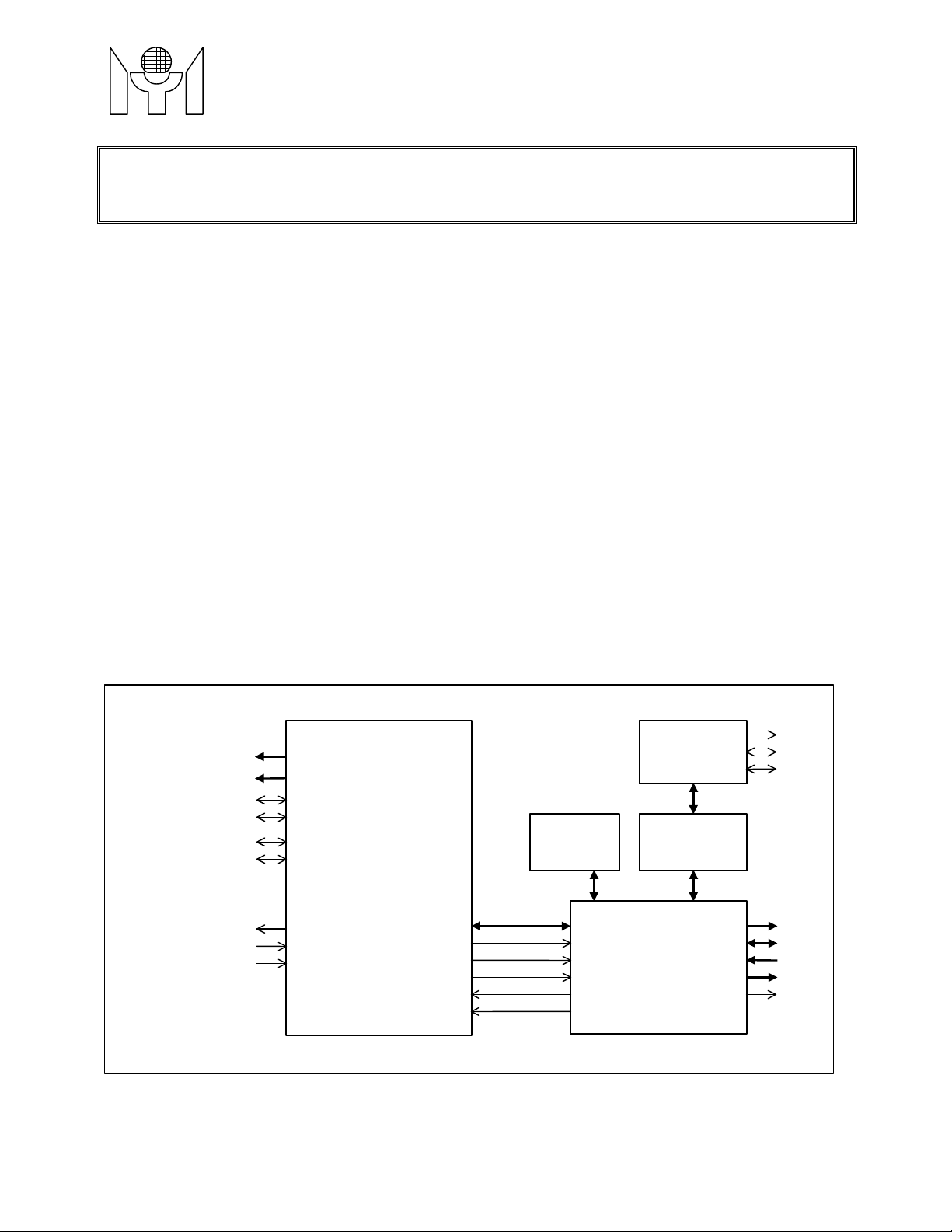
GENERAL DESCRIPTIONS
The MTP805 micro-controller is an 8051 CPU core embedded device specia lly tailored to USB/PS2
Keyboard/Mouse applications. It includes an 8051 CPU core, 256-byte SRAM, Low Speed USB Interface
and an 8K-byte internal program Flash-ROM.
BL OCK DIAGRAM
This datasheet contains new product information. Myson Technology reserv es the rights to modify the product specification without
notice. No liability is assumed as a result of the use of this product. No rights under any patent accompany the sale of the product.
Revision 0.9 - 1 - 2000/07/19
Page 2
MYSON
VSS
KSI0
KSI1
KSI2
KSI3
KSI4
KSI5
KSI6
KSI7
KSO1024KSO11
KSO12
KSO9
KSO13
KSO14
NC
KSO5
KSO6
KSO7
KSO8
23222120282726
25
KSI1
6543214443424140
KSI0
RST
OSC2
OSC1
VSS
DP/PS2CLK
DM/PS2DATA
V33
VDD
NC
19
18
VSS
KSI0
KSI1
KSI2
KSI3
KSI4
KSI5
KSI6
KSI7
VSS
KSI0
KSI1
KSI2
KSI3
KSI4
KSI5
KSI6
KSI7
MTP805
TECHNOLOGY
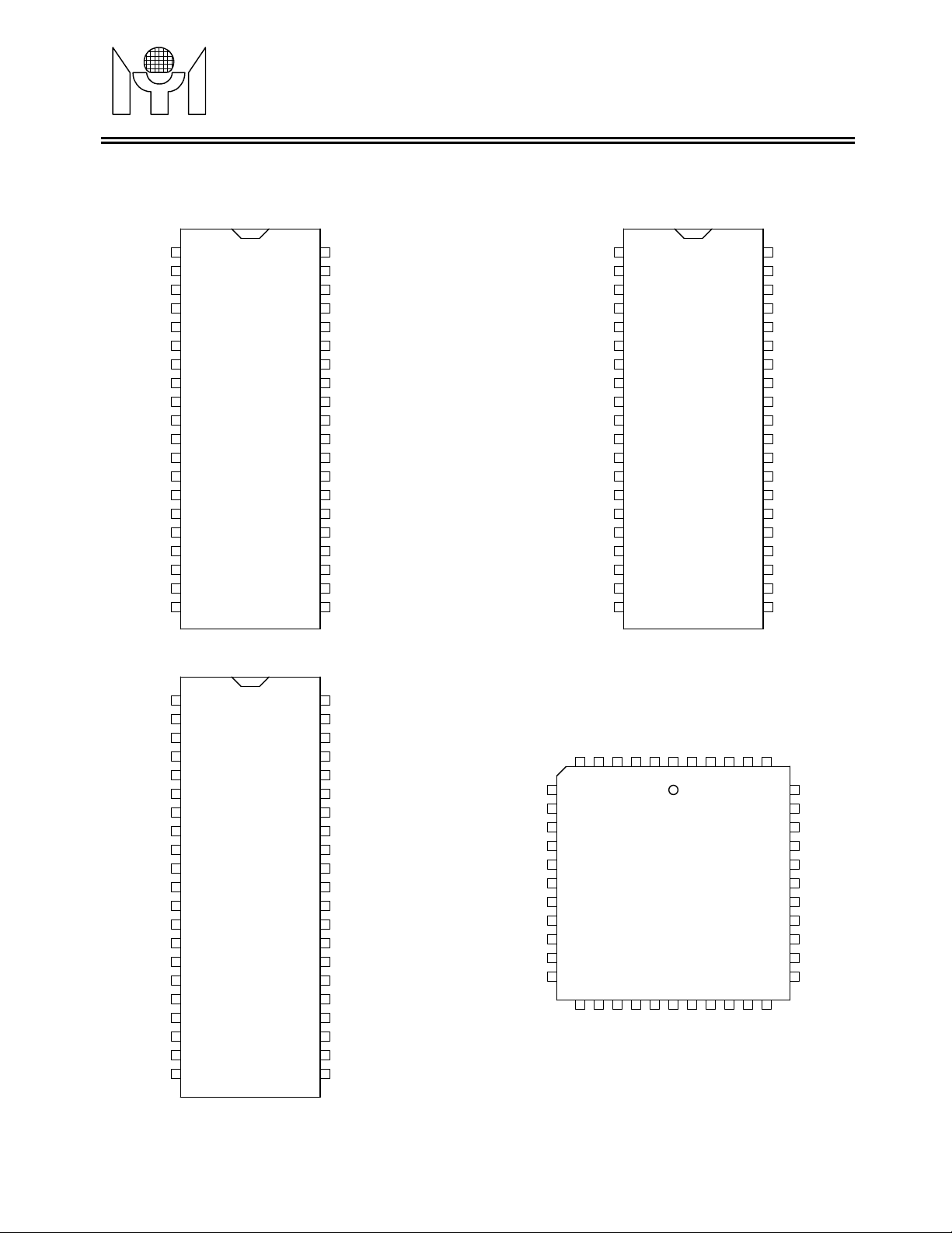
PIN CONNECTION
RST
2
3
4
5
6
7
8
9
10
11
12
13
14
15
16
17
18
19
20
MTP805
40 Pin
PDIP #1
OSC1
OSC2
KSO0
KSO1
KSO2
KSO3
KSO4
KSO5
KSO6
KSO7
401
DP/PS2CLK
39
DM/PS2DATA
38
V33
37
VDD
36
LED0
35
LED1
34
LED2
33
MSCLK
32
MSDATA
31
GPIO0
30
KSO17
29
KSO16
28
KSO15
27
KSO14
26
KSO13
25
KSO12
24
KSO11
23
KSO10
22
KSO9
21
KSO8
(Rev. 0.9)
401
OSC1
OSC2
RST
KSO0
KSO1
KSO2
KSO3
KSO4
KSO5
KSO6
KSO7
2
3
4
5
6
7
8
9
10
11
12
13
14
15
16
17
18
19
20
MTP805
40 Pin
PDIP #2
39
38
37
36
35
34
33
32
31
30
29
28
27
26
25
24
23
22
21
DP/PS2CLK
DM/PS2DATA
V33
VDD
LED0
LED1
LED2
GPO0
MSCLK
MSDATA
KSO17
KSO16
KSO15
KSO14
KSO13
KSO12
KSO11
KSO10
KSO9
KSO8
OSC1
OSC2
RST
KSO0
KSO1
KSO2
KSO3
KSO4
KSO5
KSO6
KSO7
KSO8
1
2
3
4
5
6
7
8
9
10
11
12
13
14
15
16
17
18
19
20
MTP805
42 Pin
SDIP
DP/PS2CLK
42
DM/PS2DATA
41
40
V33
39
VDD
38
LED0
37
LED1
36
LED2
35
GPO0
34
MSCLK
33
MSDATA
32
GPIO1
31
GPIO0
30
KSO17
29
KSO16
28
KSO15
27
KSO14
26
KSO13
25
KSO12
24
KSO11
23
KSO10
2221
KSO9
KSI2
KSI3
KSI4
KSI5
KSI6
KSI7
KSO0
KSO1
KSO2
KSO3
KSO4
7
8
9
10
11
12
13
14
15
16
17
MTP805
44 Pin
PLCC
39
38
37
36
35
34
33
32
31
30
29
LED0
LED1
LED2
GPO0
MSCLK
MSDATA
GPIO1
GPIO0
KSO17
KSO16
KSO15
Revision 0.9 - 2 - 2000/07/19
Page 3

MYSON
DM/PS2DATA
MTP805
TECHNOLOGY
PIN DESCRIPTION
Name Type Description
VSS
OSC1
OSC2
RST
KSI0
KSI1
KSI2
KSI3
KSI4
KSI5
KSI6
KSI7
KSO0
KSO1
KSO2
KSO3
KSO4
KSO5
KSO6
KSO7
KSO8
KSO9
KSO10
KSO11
KSO12
KSO13
KSO14
KSO15
KSO16
KSO17
GPIO0
GPIO1
MSDATA
MSCLK
GPO0
LED2
LED1
LED0
VDD
V33
DP/PS2CLK
- Ground.
I Oscillator input.
O Oscillator output.
I Active high reset. (with internal pull-down resistor)
I Key scan input 0. (Schmitt-trigger with 10K/33K/50K pull-up resistor)
I Key scan input 1. (Schmitt-trigger with 10K/33K/50K pull-up resistor)
I Key scan input 2. (Schmitt-trigger with 10K/33K/50K pull-up resistor)
I Key scan input 3. (Schmitt-trigger with 10K/33K/50K pull-up resistor)
I Key scan input 4. (Schmitt-trigger with 10K/33K/50K pull-up resistor)
I Key scan input 5. (Schmitt-trigger with 10K/33K/50K pull-up resistor)
I Key scan input 6. (Schmitt-trigger with 10K/33K/50K pull-up resistor)
I Key scan input 7. (Schmitt-trigger with 10K/33K/50K pull-up resistor)
O Key scan output 0 (8051’s P1.0). (Pseudo open-drain)
O Key scan output 1 (8051’s P1.1). (Pseudo open-drain)
O Key scan output 2 (8051’s P1.2). (Pseudo open-drain)
O Key scan output 3 (8051’s P1.3). (Pseudo open-drain)
O Key scan output 4 (8051’s P1.4). (Pseudo open-drain)
O Key scan output 5 (8051’s P1.5). (Pseudo open-drain)
O Key scan output 6 (8051’s P1.6). (Pseudo open-drain)
O Key scan output 7 (8051’s P1.7). (Pseudo open-drain)
O Key scan output 8 (8051’s P2.0). (Pseudo open-drain)
O Key scan output 9 (8051’s P2.1). (Pseudo open-drain)
O Key scan output 10 (8051’s P2.2). (Pseudo open-drain)
O Key scan output 11 (8051’s P2.3). (Pseudo open-drain)
O Key scan output 12 (8051’s P2.4). (Pseudo open-drain)
O Key scan output 13 (8051’s P2.5). (Pseudo open-drain)
O Key scan output 14 (8051’s P2.6). (Pseudo open-drain)
O Key scan output 15 (8051’s P2.7). (Pseudo open-drain)
I/O Key scan output 16. (Pseudo open-drain)
I/O Key scan output 17. (Pseudo open-drain)
I/O General purpose I/O 0. (Pseudo open-drain)
I/O General purpose I/O 1. (Pseudo open-drain)
I/O Mouse data (8051’s P3.0). (Pseudo open-drain)
I/O Mouse clock (8051’s P3.1). (Pseudo open-drain)
O General purpose output 0. (Open-drain with 420 ohm serial resistor)
O Output pin to drive LED 2. (Open-drain with 420 ohm serial resistor)
O Output pin to drive LED 1. (Open-drain with 420 ohm serial resistor)
O Output pin to drive LED 0. (Open-drain with 420 ohm serial resistor)
- Positive Power Supply.
O 3.3 Volt USB regulator output. (Must connect to 1uF or larger capacitor)
I/O USB DM / PS2 keyboard data (8051’s P3.5).
I/O USB DP / PS2 keyboard clock (8051’s P3.4).
(Rev. 0.9)
“Pseudo open-drain” pin is 8051 Port1’s standard. It can sink at least 4mA current when output low level, and
drive at least 4mA current for 2 X’tal cycle when output transit from low to high, then keep drive 100uA to
maintain the pin at high level.
Revision 0.9 - 3 - 2000/07/19
Page 4

MYSON
MTP805
TECHNOLOGY
(Rev. 0.9)
FUNCTIONAL DESCRIPTIONS
1. 8051 CPU Core
MTP805 includes all 8051 functions with the following exceptions:
1.1 PSEN, ALE, #RD and #WR pins are disabled. The external RAM access is restricted to XFRs within the
MTP805.
1.2 Port0, port3.2, port3.3, port3.6 and port3.7 are not general-purpose I/O ports. They are dedicated to
special application.
1.3 #INT0 and #INT1 input pin is not provided, it is connected to special interrupt sources.
1.4 UART and Timer1 are not supported.
Note: All registers listed in this document reside in external RAM area (XFR). For internal RAM memory map
please refer to 8051 spec.
2. Memory Allo cati on
2.1 Internal Special Function Registers (SFR)
The SFR is a group of registers that are the same as standard 8051.
2.2 Internal RAM
There are total 256 bytes internal RAM in MTP805, same as standard 8052.
2.3 External Special Function Registers (XFR)
The XFR is a group of registers allocated in the 8051 external RAM area 00h - 2Fh. Most of the registers are
used for USB function. Program can initialize Ri value and use "MOVX" instruction to access these registers.
FFh
Internal RAM
Accessible by
addressing only
MOV A,@Ri
instruction)
80h
7Fh
Internal RAM
Accessible by
direct and indirect
addressing
00h
indirect
(Using
SFR
Accessible by
direct addressing
2Fh
Accessible by
indirect external
RAM addressing
MOVX A,@Ri
00h
XFR
(Using
instruction
Revision 0.9 - 4 - 2000/07/19
Page 5
MYSON
MTP805
TECHNOLOGY
(Rev. 0.9)
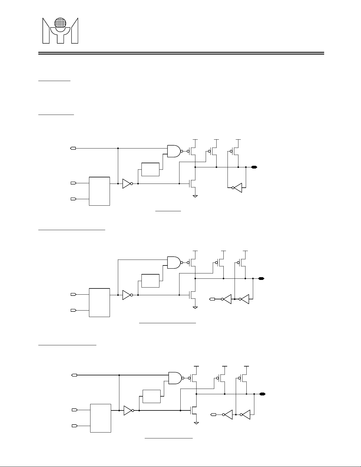
3. I/O Pin Usage
3.1 KSO0~7
These pins are direct output from the 8051’s Port1 and dedicated for key scan output. The pin’s input
function is removed. Read 8051’s Port1 is only read the data in the Port1’s output register. These pins are
“Pseudo open-drain” structure.
3.2 KSO8~15
These pins are direct output from the 8051’s Port2 and dedicated for key scan output. The pin’s input
function is removed. Read 8051’s Port2 is only read the data in the Port2’s output register. These pins are
“Pseudo open-drain” structure.
Read
Data
Write
Data
/WR
Output
Register
CK
4mA 50uA
2 OSC
period
delay
QD
4mA
500uA
Pin
KSO0~15
3.3 KSO16~17, GPIO0~1
These pins are output from MTP805’s XFR. They can be used as key scan output or general purpose I/O.
Read these pins will read the data on pin. These pins are also “Pseudo open-drain” structure.
Write
Data
/WR
Output
Register
CK
4mA 50uA
1 OSC
period
delay
QD
4mA
Read
Data
500uA
Pin
KSO16~17, GPIO0~1
3.4 MSCLK, MSDATA
These pins are connected to 8051’s P3.1 and P3.0. The usage of these pins are the same as standard 8051
except the UART’s function being not provided. These pins are also “Pseudo open-drain” structure.
Read
Latch
Data
Write
Data
/WR
Output
Register
CK
4mA 50uA
2 OSC
period
delay
QD
4mA
Read
Pin
Data
500uA
Pin
MSCLK, MSDATA
Revision 0.9 - 5 - 2000/07/19
Page 6

MYSON
MTP805
TECHNOLOGY
(Rev. 0.9)
3.5 PS2CLK, PS2DATA
These pins are shared with USB’s DP/DM pins. They are connected to 8051’s P3.4 and P3.5. In PS2 mode,
S/W should keep “ENUSB”=0 and “PS2KB”=1. In USB mode, S/W should keep “ENUSB”=1, “PS2KB”=0 and
P3.4/P3.5 output high. These pins are also “Pseudo open-drain” structure in PS2 mode.
3.3V
Read
Latch
Data
Write
Data
/WR
Output
Register
CK
2 OSC
period
delay
QD
PS2KB
4mA 20uA
4mA
USBSIE
Output
Read
Pin
Data
Pin
DP/PS2CLK, DM/PS2DATA
3.6 LED0~2, GPO0
These pins are used to drive LED. Basically, they are open-drain structure. Each one has a 420 ohm serial
resistor when sink pin to low, and has a 100K resistor when drive high. S/W may write data to “LED” register
to control these pins’ status. Read “LED” only read the data in the “LED” register, instead of data on the pins.
Read
Data
Write
Data
/WR
Output
Register
CK
QD
50uA
Pin
420
4mA
LED0~2, GPO0
3.7 KSI0~7
These pins are used as key scan input. Reading “KSI” register of XFR reflect the data on the pin. These pins
are input only with pull-up resistor on each pin.
Read
Data
Pin
KSI0~7
Revision 0.9 - 6 - 2000/07/19
Page 7

MYSON
MTP805
TECHNOLOGY
4. USB and PS2 Mode Detecti o n
After reset, the USB transceiver is disable, and the V33 pin is in high impedance state (no 3.3 volt output).
S/W can detect the application is USB mode or PS2 mode by reading P3.4/P3.5. At firs t, S/W can set
“PS2KB”=1. This control bit is used to enable the internal 250K pull-up resistor on DP/DM pin. If the chip is
connected to USB Hub, the P3.4/P3.5 is 0 because of the 15K pull-down resistor on Hub. Otherwise,
P3.4/P3.5 is 1.
5. Power-dow n and Idle Mode
The Power-down/Idle mode is activated by S/W setting the PD/IDL bit in 8051’s PCON register. In Powerdown mode, the MTP805’s X’tal stop oscillating. In Idle mode, the 8051’s instruction clock is stop. The
Power-down/Idle mode is released by any enable interrupt. For standard 8051, Power-down mode is
released only by chip reset.
6. Watch-Dog-Timer(WDT) and Lo w-Volt age-Reset(LVR)
The WDT is enable by setting the “WDTen” bit in XFR. The time out period is 0.64 second. S/W can clear
WDT by writing the WDT register.
The LVR can generate chip reset when VDD is below 3.0 volt, including both power-on and power-off
process.
(Rev. 0.9)
7. Fast Clock Optio n
The CPU can run at double clock rate when S/W setting the “FCLKen” bit in XFR. Once setting, the 8051 is
running at the rate as if a 12MHz X’tal is on OSC pins. However, S/W must clear the FCLKen bit before
entering Power-down mode.
8. USB Engine
The USB engine includes the Serial Interface Engine (SIE), the low-speed USB I/O transceiver and the 3.3
Volt Regulator. The SIE block performs most of the USB interface function with only minimum support from
S/W. Three endpoints are supported. Endpoint 0 is used to receive and transmit control (including SETUP)
packets while Endpoint 1 and endpoint 2 are only used to transmit data packets.
The USB SIE handles the following USB bus activity independently:
1. Bitstuffing/unstuffing
2. CRC generation/checking
3. ACK/NAK
4. TOKEN type identification
5. Address checking
S/W handles the following tasks:
1. Coordinate enumeration by responding to SETUP packets
2. Fill and empty the FIFOs
3. Suspend/Resume coordination
4. Verify and select DATA toggle values
8.1 USB Device Address
The USBADR register stores the device address. This register is reset to all 0 af ter chip rese t or USB bus
reset. S/W must write this register a valid value after the USB enumeration process .
8.2 Endpoint 0 receive
After receiving a packet and placing the data into the Endpoint 0 receive FIFO (RC0FIFO), MTP805 updates
the Endpoint 0 status register (EP0STUS) to record the receive status and then generates an Endpoint 0
Revision 0.9 - 7 - 2000/07/19
Page 8

MYSON
MTP805
TECHNOLOGY
receive interrupt (RC0I). S/W can read the EP0STUS register for the recent transfer information, which
includes the data byte count (RC0cnt), data direction (EP0dir), SETUP token flag (EP0set) and data valid
flag (RC0err). The received data is always stored into RC0FIFO and the RC0cnt is a lways updated for DATA
packets following SETUP tokens. The data following an OUT token is written into the RC0FIFO, and the
RC0cnt is updated unless Endpoint 0 STALL (EP0stall) is set or Endpoint 0 receive ready (RC0rdy) is
cleared. The SIE clears the RC0rdy automatically and generates RC0I interrupt when the RC0cnt/RC0FIFO
is updated. As long as the RC0rdy is cleared, SIE keep responding NAK to Host’s Endpoint 0 OUT packet
request. S/W should set the RC0rdy flag after the RC0I interrupt is asserted and RC0FIFO is read out.
8.3 Endpoint 0 transmit
After detecting a valid Endpoint 0 IN token, MTP805 automatically transmit the data pre-stored in the
Endpoint 0 transmit FIFO (TX0FIFO) to the USB bus if the Endpoint 0 transmit ready flag (TX0rdy) is set and
the EP0stall is cleared. The number of byte to be transmitted is base on the Endpoint 0 transmit byte count
register (TX0cnt). The DATA0/1 token to be transmitted is base on the Endpoint 0 transmit toggle control bit
(TX0tgl). After the TX0FIFO is updated, TX0rdy should be set to 1. This enables the MTP805 to respond to
an Endpoint 0 IN packet. TX0rdy is cleared and an Endpoint 0 transmit interrupt (TX0I) is generated once the
USB host acknowledges the data transmission. The interrupt service routine can check TX0rdy to confirm
that the data transfer was successful.
8.4 Endpoint 1/2 transmit
Endpoint1 and Endpoint2 are capable of transmit only. These endpoints are ena ble when the Endpoint1/
Endpoint2 configured control bit (EP1cfgd/EP2cfgd) is set. After detecting a valid Endp oint 1/2 IN token,
MTP805 automatically transmit the data pre-stored in the Endpoint 1/2 transmit FIFO (TX1FIFO/TX2FIFO) to
the USB bus if the Endpoint 1/2 transmit ready flag (TX1rd y/TX2rdy) is set and the EP1stall/EP2stall is
cleared. The number of byte to be transmitted is base on the Endpoint 1/2 transmit byte count register
(TX1cnt/TX2cnt). The DATA0/1 token to be transmitted is base on the Endpoint 1/2 tra nsmit toggle control
bit (TX1tgl/TX2tgl). After the TX1FIFO/TX2FIFO is updated, TX1rdy/TX2rdy should be set to 1. This enables
the MTP805 to respond to an Endpoint 1/2 IN packet. TX1rdy/TX2rdy is cleared and an Endpoint 1/2
transmit interrupt (TX1I/TXI2) is generated once the USB host acknowledges the dat a transmission. The
interrupt service routine can check TX1rdy/TX2rdy to confirm that the data transfer was successful.
(Rev. 0.9)
8.5 USB Control and Status
Other USB control bits include the USB enable (ENUSB), SUSPEND (Susp), RESUME (RsmO), Control
Read (CtrRD), and corresponding interrupt enable bits. The CtrRD should be set when program detects the
current transfer is an Endpoint0 Control Read Transfer. Once this bit is set, the MTP8 05 will stall an
Endpoint0 OUT packet with DATA toggle 0 or byte count other than 0. Other US B stat us flag includes the
USB reset interrupt (RstI), RESUME interrupt (RsmI), and USB Suspend interrupt (SusI).
8.6 Suspend and Resume
Once the Suspend condition is asserted, S/W can set the Susp bit to stop the USBSIE's clock. In the mean
time, the 3.3V Regulator is operating in low power mode. S/W can further save the device power by force the
8051 CPU core into the Power Down or Idle mode by setting the PCON register in SFR area. In the Idel
mode, the X'tal keeps oscillating and CPU can be waken-up by the trigger of any enabled interrupt. In the
Power Down mode, the X'tal is stop, but CPU can be waken-up by the trigger of enabled interrupt's source.
In short, S/W can keep the RsmI/KbdI/MsI alive before enter the suspend mode.
The MTP805 send Resume signaling to USB bus when Susp=1 and RSMO=1. In the suspend mode, if a
keyboard or mouse interrupt is asserted, S/W should send resume signal to wake up the USB bus.
Revision 0.9 - 8 - 2000/07/19
Page 9

MYSON
WDTen
MTP805
TECHNOLOGY
(Rev. 0.9)
MEMORY MAP of XFR
Reg name addr bit7 bit6 bit5 Bit4 bit3 bit2 bit1 bit0
USBADR
INTFLG0
INTEN0
INTFLG1
INTEN1
USBCTR
EP0STUS
TX0CTR
TX1CTR
TX2CTR
KSI
LED
GPIO
WDT
KSIMASK
RC0FIFO
RC0FIFO
RC0FIFO
RC0FIFO
RC0FIFO
RC0FIFO
RC0FIFO
RC0FIFO
TX0FIFO
TX0FIFO
TX0FIFO
TX0FIFO
TX0FIFO
TX0FIFO
TX0FIFO
TX0FIFO
TX1FIFO
TX1FIFO
TX1FIFO
TX1FIFO
TX1FIFO
TX1FIFO
TX1FIFO
TX1FIFO
TX2FIFO
TX2FIFO
TX2FIFO
TX2FIFO
TX2FIFO
TX2FIFO
TX2FIFO
TX2FIFO
00h (r/w) ENUSB USBadr
01h (r/w) RC0I TX0I TX1I TX2I RstI SusI
02h (w) RC0IE TX0IE TX1IE TX2IE RstIE SusIE
03h (r/w) RsmI KbdI MsI
04h (w) PS2KB FclkE RsmIE KbdIE MsIE
05h (r/w) Susp RsmO EP1cfgd EP2cfgd RC0rdy CtrRD
06h (r) RC0tgl RC0err EP0dir EP0set RC0cnt
07h (r/w) TX0rdy TX0tgl EP0stall TX0cnt (write only)
08h (r/w) TX1rdy TX1tgl EP1stall TX1cnt (write only)
09h (r/w) TX2rdy TX2tgl EP2stall TX2cnt (write only)
0Ah (r) KSI7 KSI6 KSI5 KSI4 KSI3 KSI2 KSI1 KSI0
0Bh (r/w) GPO0 LED2 LED1 LED0
0Ch (r/w) GPIO1 GPIO0 KSO17 KSO16
0Dh (w)
0Eh (w) KSImsk7 KSImsk6 KSImsk5 KSImsk4 KSImsk3 KSImsk2 KSImsk1 KSImsk0
10h (r) Endpoint 0 receive FIFO 1st byte
11h (r) Endpoint 0 receive FIFO 2nd byte
12h (r) Endpoint 0 receive FIFO 3rd byte
13h (r) Endpoint 0 receive FIFO 4th byte
14h (r) Endpoint 0 receive FIFO 5th byte
15h (r) Endpoint 0 receive FIFO 6th byte
16h (r) Endpoint 0 receive FIFO 7th byte
17h (r) Endpoint 0 receive FIFO 8th byte
18h (w) Endpoint 0 transmit FIFO 1st byte
19h (w) Endpoint 0 transmit FIFO 2nd byte
1Ah (w) Endpoint 0 transmit FIFO 3rd byte
1Bh (w) Endpoint 0 transmit FIFO 4th byte
1Ch (w) Endpoint 0 transmit FIFO 5th byte
1Dh (w) Endpoint 0 transmit FIFO 6th byte
1Eh (w) Endpoint 0 transmit FIFO 7th byte
1Fh (w) Endpoint 0 transmit FIFO 8th byte
20h (w) Endpoint 1 transmit FIFO 1st byte
21h (w) Endpoint 1 transmit FIFO 2nd byte
22h (w) Endpoint 1 transmit FIFO 3rd b yte
23h (w) Endpoint 1 transmit FIFO 4th byte
24h (w) Endpoint 1 transmit FIFO 5th byte
25h (w) Endpoint 1 transmit FIFO 6th byte
26h (w) Endpoint 1 transmit FIFO 7th byte
27h (w) Endpoint 1 transmit FIFO 8th byte
28h (w) Endpoint 2 transmit FIFO 1st byte
29h (w) Endpoint 2 transmit FIFO 2nd byte
2Ah (w) Endpoint 2 transmit FIFO 3rd byte
2Bh (w) Endpoint 2 transmit FIFO 4th byte
2Ch (w) Endpoint 2 transmit FIFO 5th byte
2Dh (w) Endpoint 2 transmit FIFO 6th byte
2Eh (w) Endpoint 2 transmit FIFO 7th byte
2Fh (w) Endpoint 2 transmit FIFO 8th byte
Revision 0.9 - 9 - 2000/07/19
Page 10

MYSON
MTP805
TECHNOLOGY
USBADR (r/w) :USB device address and enable.
ENUSB = 1 → Enable USB function, clear while chip reset.
USBadr : USB device address, clear while chip reset or USB bus reset.
INTFLG0 (w) : Interrupt flag. A interrupt event will set its individual flag, and, if the corresponding interrupt
enable bit is set, the 8051’s INT0 source will be driven by a zero level. Software MUST clear
this register while serve the interrupt routine.
RC0I = 1 → No action.
= 0 → Clear RC0I flag.
TX0I = 1 → No action.
= 0 → Clear TX0I flag.
TX1I = 1 → No action.
= 0 → Clear TX1I flag.
TX2I = 1 → No action.
= 0 → Clear TX2I flag.
RstI = 1 → No action.
= 0 → Clear RstI flag.
SusI = 1 → No action.
= 0 → Clear SusI flag.
INTFLG0 (r) : Interrupt flag.
RC0I = 1 → Endpoint 0 has completed a receive transfer and save the data in RC0FIFO.
TX0I = 1 → Endpoint 0 has completed a transmit transfer and empty TX0FIFO.
TX1I = 1 → Endpoint 1 has completed a transmit transfer and empty TX1FIFO.
TX2I = 1 → Endpoint 2 has completed a transmit transfer and empty TX2FIFO.
RstI = 1 → Indicates the USB bus reset condition.
SusI = 1 → Indicates the USB bus suspend request (no bus activity for 3ms).
(Rev. 0.9)
INTEN0 (w) : Interrupt enable.
RC0IE = 1 → Enable RC0I interrupt.
TX0IE = 1 → Enable TX0I interrupt.
TX1IE = 1 → Enable TX1I interrupt.
TX2IE = 1 → Enable TX2I interrupt.
RstIE = 1 → Enable RstI interrupt.
SusIE = 1 → Enable SusI interrupt.
INTFLG1 (w) : Interrupt flag. A interrupt event will set its individual flag, and, if the corresponding interrupt
enable bit is set, the 8051’s INT1 source will be driven by a zero level. Software MUST clear
this register while serve the interrupt routine.
RsmI = 1 → No action.
= 0 → Clear RsmI flag.
KbdI = 1 → No action.
= 0 → Clear KbdI flag.
MsI = 1 → No action.
= 0 → Clear MsI flag.
INTFLG1 (r) : Interrupt flag.
RsmI = 1 → Indicates the USB bus RESUME condition in suspend mode.
KbdI = 1 → Indicates a low input has been detected on anyone of the KSI pins.
MsI = 1 → Indicates a low input has been detected on the MSCLK pin.
INTEN1 (w) : Interrupt enable.
PS2KB = 1 → Enable the pull up resistors on DP/PS2CLK and DM/PS2DATA pins.
FclkE = 1 → Enable the CPU’s faster clock, MUST be cleared before power-down.
Revision 0.9 - 10 - 2000/07/19
Page 11

MYSON
MTP805
TECHNOLOGY
RsmIE = 1 → Enable RsmI interrupt.
KbdIE = 1 → Enable KbdI interrupt.
MsIE = 1 → Enable MsI interrupt.
USBCTR (r/w) :USB control register.
Susp = 1 → S/W force USB interface into suspend mode.
RsmO = 1 → S/W force USB interface send RESUME signal in suspend mode.
EP1cfgd = 1 → Endpoint 1 is configed.
EP2cfgd = 1 → Endpoint 2 is configed.
RC0rdy = 1 → Enable the Endpoint 0 to respond to OUT token.
= 0 → Endpoint 0 will respond NAK to OUT token.
This bit can be set or cleared by S/W, clear by H/W while RC0I occurs.
CtrRD = 1 → MTP805 will stall an invalid OUT token during Control Read transfer.
EP0STUS (r) : Endpoint 0 status.
RC0tgl = 1 → Receive a DATA1 packet.
= 0 → Receive a DATA0 packet.
RC0err = 1 → Receive DATA packet error.
= 0 → Receive DATA packet good.
EP0dir = 1 → Last transfer is transmit direction (IN).
= 0 → Last transfer is receive direction (OUT, SETUP).
EP0set = 1 → Last transfer is a SETUP.
= 0 → Last transfer is not a SETUP.
RC0cnt : Last transfer's receive byte count.
(Rev. 0.9)
TX0CTR (r/w) : Endpoint 0 transmit control register.
TX0rdy = 1 → Enable the Endpoint 0 to respond to IN token.
= 0 → Endpoint 0 will respond NAK to IN token.
This bit can be set or cleared by S/W, clear by H/W while Host ack the transfer.
TX0tgl = 1 → Endpoint 0 will transmit DATA1 packet.
= 0 → Endpoint 0 will transmit DATA0 packet.
EP0stall = 1 → Endpoint 0 will stall OUT/IN packet.
TX0cnt (w) : Endpoint 0 transmit byte count, write only.
TX1CTR (r/w) : Endpoint 1 transmit control register.
TX1rdy = 1 → Enable the Endpoint 1 to respond to IN token.
= 0 → Endpoint 1 will respond NAK to IN token.
This bit can be set or cleared by S/W, clear by H/W while Host ack the transfer.
TX1tgl = 1 → Endpoint 1 will transmit DATA1 packet.
= 0 → Endpoint 1 will transmit DATA0 packet.
EP1stall = 1 → Endpoint 1 will stall IN packet.
TX1cnt (w) : Endpoint 1 transmit byte count, write only.
TX2CTR (r/w) : Endpoint 1 transmit control register.
TX2rdy = 1 → Enable the Endpoint 2 to respond to IN token.
= 0 → Endpoint 2 will respond NAK to IN token.
This bit can be set or cleared by S/W, clear by H/W while Host ack the transfer.
TX2tgl = 1 → Endpoint 2 will transmit DATA1 packet.
= 0 → Endpoint 2 will transmit DATA0 packet.
EP2stall = 1 → Endpoint 2 will stall IN packet.
TX2cnt (w) : Endpoint 1 transmit byte count, write only.
KSI (r) : KSI7~0’s read result.
LED (w) : Data load into the GPO0 / LED2~0 output latch.
Revision 0.9 - 11 - 2000/07/19
Page 12

MYSON
MTP805
TECHNOLOGY
LED (r) : Data read from the GPO0 / LED2~0 output latch.
GPIO (w) : Data load into the GPIO1~0 / KSO17~16 output latch.
GPIO (r) : Data read from the GPIO1~0 / KSO17~16 pin.
WDT (w) : Write this register to clear Watch-Dog-Timer.
WDTen= 1 → Enable Watch-Dog-Timer.
KSIMASK (w) : Determine whether the key scan input can generate interrupt or not.
KSImsk(n) = 1 → KSI(n) can not generate keyboard interrupt.
KSImsk(n) = 0 → KSI(n) can generate keyboard interrupt.
RC0FIFO (r) : Endpoint 0 receive FIFO registers.
TX0FIFO (w) : Endpoint 0 transmit FIFO registers.
TX1FIFO (w) : Endpoint 1 transmit FIFO registers.
TX2FIFO (w) : Endpoint 2 transmit FIFO registers.
(Rev. 0.9)
Revision 0.9 - 12 - 2000/07/19
Page 13

MYSON
MTP805
TECHNOLOGY
(Rev. 0.9)
ELECTRICAL PARA METERS
1. Absolu t e Maximum Ratings
at: Ta= 0 to 70 oC, VSS=0V
Name Symbol Range Unit
Maximum Supply Voltage VDD -0.3 to +6.0 V
Maximum Input Voltage Vin -0.3 to VDD+0.3 V
Maximum Output Voltage Vout -0.3 to VDD+0.3 V
Maximum Operating Temperature Topg 0 to +70 o
Maximum Storage Temperature Tstg -25 to +125 o
2. Allowable Operating Condit io n s
at: Ta= 0 to 70 oC, VSS=0V
Name Symbol Min. Max. Unit
Supply Voltage VDD 4.5 5.5 V
Input "H" Voltage Vih1 0.7 x VDD VDD +0.3 V
Input "L" Voltage Vil1 -0.3 0.15 x VDD V
Operating Freq. Fosc 6 6 MHz
C
C
3. DC Characteri s t i c s
at: Ta= 25 oC, VSS=0V, VDD=5V, Fosc=6MHz
Name Symbol Min. Max. Unit
Active current Icc 6 mA
Power Down current Ipd 20 uA
Output High Voltage @ Ioh=-100u Voh 4.0 V
Output Low Voltage @ Iol=4mA Vol 0.45 V
LED sink current @ Vol=3.2V Iled 6.2 m A
RST pin pull down resistor Rrst 50 150 Kohm
KSI pin pull up resistor Rksi 50 100 Kohm
V33 output voltage V33 3.2 3.4 V
4. AC Characterist ic s
at: Ta= 25 oC, VSS=0V, VDD=5V, Fosc=6MHz
Name Symbol Min. Max. Unit
DP/DM rise time Trise 75 300 ns
DP/DM fall time Tfall 75 300 ns
DP,DM cross point Vx 1.3 2.0 V
* note: all USB transceiver characteristic can meet USB 1.1 spec
Revision 0.9 - 13 - 2000/07/19
Page 14

MYSON
MTP805
TECHNOLOGY
PACKAGE DIMENSION
1. 40-pin PDIP 600 mil
1.981mm
+/-0.254
3.81mm
+/-0.127
3.302mm
+/-0.254
2. 42 pin SDIP Unit: mm
52.197mm +/-0.127
2.540mm0.457mm +/-0.1271.270mm +/-0.254
(Rev. 0.9)
15.494mm +/-0.254
1.778mm
+/-0.127
0.254mm
(min.)
13.868mm +/-0.102
5o~7
16.256mm +/-0.508
0
6o +/-3
0.254mm
o
+/-0.102
Symbol
Dimension in mm
Min Nom Max
A 3.937 4.064 4.2
A1 1.78 1.842 1.88
B1 0.914 1.270 1.118
D 36.78 36.83 36.88
E1 13.9 45 13.970 13.995
F 15.19 15.240 15.29
eB 15.24 16.510 17.78
θ 0° 7.5° 15°
15.494mm +/-
0.254
13.868mm +/-
0.102
5o~7
16.256mm +/-
0.508
0
6o +/-
3
0.254m
m
+/-0.102
o
Revision 0.9 - 14 - 2000/07/19
Page 15

MYSON
MTP805
3. 44 pin PLCC Unit:
0
0.045*45
0.050 TYP.
0.653 +/-0.003
0.690 +/-0.005
TECHNOLOGY
PIN #1 HOLE
0.690 +/-0.005
0.653 +/-0.003
0.026~0.032 TYP.
(Rev. 0.9)
0.180 MAX.
0.013~0.021 TYP.
70TYP.
0.070 0.070
0.020 MIN.
0.610 +/-0.02
0.500
0.010
Ordering Inform ation
Standard configurations:
Prefix Part Typ e Package Type
N: PDIP
MTP 805
Part Numbers:
Prefix Part Type Package Type
MTP 805 N
MTP 805 S
MTP 805 V
S: SDIP
V: PLCC
Revision 0.9 - 15 - 2000/07/19
 Loading...