

Page 1
SEMICONDUCTOR TECHNICAL DATA
N–Channel Enhancement–Mode Silicon Gate
This advanced high voltage TMOS E–FET is designed to
withstand high energy in the avalanche mode and switch efficiently .
This new high energy device also offers a drain–to–source diode
with fast recovery time. Designed for high voltage, high speed
switching applications such as power supplies, PWM motor
controls and other inductive loads, the avalanche energy capability
is specified to eliminate the guesswork in designs where inductive
loads are switched and offer additional safety margin against
unexpected voltage transients.
• Avalanche Energy Capability Specified at Elevated
Temperature
• Low Stored Gate Charge for Efficient Switching
• Internal Source–to–Drain Diode Designed to Replace External
Zener Transient Suppressor — Absorbs High Energy in the
Avalanche Mode
• Source–to–Drain Diode Recovery Time Comparable to Discrete
Fast Recovery Diode
G
Order this document
by MTP3N60E/D
Motorola Preferred Device
TMOS POWER FET
3.0 AMPERES
600 VOL TS
R
D
S
DS(on)
= 2.2 OHMS
CASE 221A–09, Style 5
TO-220AB
MAXIMUM RATINGS
Drain–Source Voltage V
Drain–Gate Voltage (RGS = 1.0 MΩ) V
Gate–Source Voltage — Continuous
Gate–Source Voltage — Non–repetitive
Drain Current — Continuous
Drain Current — Continuous @ 100°C
Drain Current — Pulsed
Total Power Dissipation @ TC = 25°C
Derate above 25°C
Operating and Storage Temperature Range TJ, T
UNCLAMPED DRAIN–TO–SOURCE AVALANCHE CHARACTERISTICS (T
Single Pulse Drain–to–Source Avalanche Energy — TJ = 25°C
Single Pulse Drain–to–Source Avalanche Energy — TJ = 100°C
Repetitive Pulse Drain–to–Source Avalanche Energy
(TC = 25°C unless otherwise noted)
Rating Symbol Value Unit
< 150°C)
J
V
V
I
W
DSR(1)
W
DSR(2)
DSS
DGR
GS
GSM
I
D
I
D
DM
P
D
stg
600 Vdc
600 Vdc
±20
±40
3.0
2.4
14
75
0.6
–55 to 150 °C
290
46
7.5
Vdc
Vpk
Adc
Watts
W/°C
mJ
THERMAL CHARACTERISTICS
Thermal Resistance — Junction to Case°
Thermal Resistance — Junction to Ambient°
Maximum Lead Temperature for Soldering Purposes, 1/8″ from case for 10 seconds T
(1) VDD = 50 V, ID = 3.0 A
(2) Pulse Width and frequency is limited by TJ(max) and thermal response
Designer’s Data for “Worst Case” Conditions — The Designer’s Data Sheet permits the design of most circuits entirely from the information presented. SOA Limit
curves —representing boundaries on device characteristics — are given to facilitate “worst case” design.
E–FET and Designer’s are trademarks of Motorola, Inc. TMOS is a registered trademark of Motorola, Inc.
Preferred devices are Motorola recommended choices for future use and best overall value.
REV 2
R
R
θJC
θJA
L
1.67
62.5
260 °C
°C/W
Motorola TMOS Power MOSFET Transistor Device Data
Motorola, Inc. 1997
1
Page 2
MTP3N60E
)
f = 1.0 MHz)
R
100 Ω, R
12 Ω
GS(on)
)
)
V
GS
V)
ELECTRICAL CHARACTERISTICS
OFF CHARACTERISTICS
Drain–to–Source Breakdown Voltage
(VGS = 0, ID = 250 µAdc)
Zero Gate Voltage Drain Current
(VDS = 600 V, VGS = 0)
(VDS = 480 V, VGS = 0, TJ = 125°C)
Gate–Body Leakage Current — Forward (V
Gate–Body Leakage Current — Reverse (V
ON CHARACTERISTICS*
Gate Threshold Voltage
(VDS = VGS, ID = 250 µAdc)
(TJ = 125°C)
Static Drain–to–Source On–Resistance (VGS = 10 Vdc, ID = 1.5 A) R
Drain–to–Source On–Voltage (VGS = 10 Vdc)
(ID = 3.0 A)
(ID = 1.5 A, TJ = 100°C)
Forward Transconductance (VDS = 15 Vdc, ID = 1.5 A) g
DYNAMIC CHARACTERISTICS
Input Capacitance
Output Capacitance
Transfer Capacitance
SWITCHING CHARACTERISTICS*
Turn–On Delay Time
Rise Time
Turn–Off Delay Time
Fall Time
Total Gate Charge
Gate–Source Charge
Gate–Drain Charge
SOURCE–DRAIN DIODE CHARACTERISTICS
Forward On–Voltage
Forward Turn–On Time
Reverse Recovery Time t
INTERNAL PACKAGE INDUCTANCE
Internal Drain Inductance
(Measured from the contact screw on tab to center of die)
(Measured from the drain lead 0.25″ from package to center of die)
Internal Source Inductance
(Measured from the source lead 0.25″ from package to source bond pad)
*Pulse T est: Pulse Width = 300 µ s, Duty Cycle ≤ 2.0%.
**Limited by circuit inductance.
(T
= 25°C unless otherwise noted)
J
Characteristic
GSF
GSR
(IS = 3.0 A, di/dt = 100 A/µs)
= 20 Vdc, VDS = 0) I
= 20 Vdc, VDS = 0) I
(VDS = 25 V, VGS = 0,
f = 1.0 MHz
(VDD = 300 V, ID ≈ 3.0 A,
=
L
V
GS(on)
(VDS = 420 V, ID = 3.0 A,
V
G
= 10 V)
= 10 V
= 10
=
,
Symbol Min Typ Max Unit
V
(BR)DSS
I
DSS
GSSF
GSSR
V
GS(th)
DS(on)
V
DS(on)
FS
C
iss
C
oss
C
rss
t
d(on)
t
r
t
d(off)
t
f
Q
g
Q
gs
Q
gd
V
SD
t
on
rr
L
d
L
s
600 — — Vdc
—
—
— — 100 nAdc
— — 100 nAdc
2.0
1.5
— 2.1 2.2 Ohms
—
—
1.5 — — mhos
— 770 — pF
— 105 —
— 19 —
— 23 — ns
— 34 —
— 58 —
— 35 —
— 28 31 nC
— 5.0 —
— 17 —
— — 1.4 Vdc
— ** —
— 400 —
—
—
— 7.5 —
—
—
—
—
—
—
3.5
4.5
10
100
4.0
3.5
9.0
7.5
—
—
µAdc
Vdc
Vdc
ns
nH
2
Motorola TMOS Power MOSFET Transistor Device Data
Page 3
TYPICAL ELECTRICAL CHARACTERISTICS
D
MTP3N60E
8
6
4
, DRAIN CURRENT (AMPS)
2
D
I
0
10
8
6
VGS = 10 V
7 V
6 V
5 V
2 6 10 14 18
VDS, DRAIN–TO–SOURCE VOL TAGE (VOLTS)
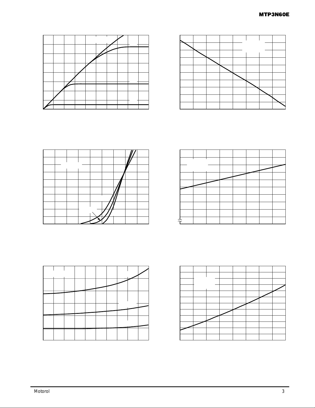
Figure 1. On–Region Characteristics
VDS ≥ 10 V
1.2
VDS = V
GS
1.1
1
0.9
0.8
, GATE THRESHOLD VOLTAGE (NORMALIZE
201612840
0.7
–50 –25 0 25 50 75 100 125 150
GS(th)
V
TJ, JUNCTION TEMPERATURE (°C)
ID = 0.25 mA
Figure 2. Gate–Threshold V oltage Variation
With Temperature
1.2
VGS = 0
1.1
ID = 250
µ
A
1
4
, DRAIN CURRENT (AMPS)
D
I
2
0
6
4
2
, DRAIN–TO–SOURCE RESIST ANCE (OHMS)
0
DS(on)
R
0.9
100°C
TJ = 25°C
1 3 5 7 9 –25 25 75 125
VGS, GATE–T O–SOURCE VOLTAGE (VOLTS)
–55°C
86420
Figure 3. Transfer Characteristics
(NORMALIZED)
0.8
, DRAIN–TO–SOURCE BREAKDOWN VOL TAGE
–50 0 50 100 150
BR(DSS)
V
TJ, JUNCTION TEMPERATURE (°C)
Figure 4. Breakdown V oltage Variation
With Temperature
3
VGS = 10 V
ID, DRAIN CURRENT (AMPS)
100°C
TJ = 25°C
–55°C
8
VGS = 10 V
ID = 2 A
2
1
(NORMALIZED)
, DRAIN–TO–SOURCE ON–RESISTANCE
DS(on)
0
R
106420
–50 0 50 100 150–25 25 75 125
TJ, JUNCTION TEMPERATURE (°C)
Figure 5. On–Resistance versus Drain Current
Motorola TMOS Power MOSFET Transistor Device Data
Figure 6. On–Resistance Variation
With Temperature
3
Page 4

MTP3N60E
SAFE OPERATING AREA INFORMATION
100
VGS = 20 V
SINGLE PULSE
TC = 25
°
10
1
, DRAIN CURRENT (AMPS)
D
I
0.1
1
C
1 ms
10 ms
dc
R
LIMIT
DS(on)
THERMAL LIMIT
PACKAGE LIMIT
10
VDS, DRAIN–TO–SOURCE VOL TAGE (VOLTS)
100
10 µs
100 µs
1000
Figure 7. Maximum Rated Forward Biased
Safe Operating Area
FORWARD BIASED SAFE OPERATING AREA
The FBSOA curves define the maximum drain–to–source
voltage and drain current that a device can safely handle
when it is forward biased, or when it is on, or being turned on.
Because these curves include the limitations of simultaneous
high voltage and high current, up to the rating of the device,
they are especially useful to designers of linear systems. The
curves are based on a case temperature of 25°C and a maximum junction temperature of 150°C. Limitations for repetitive
pulses at various case temperatures can be determined by
using the thermal response curves. Motorola Application
Note, AN569, “Transient Thermal Resistance–General Data
and Its Use” provides detailed instructions.
SWITCHING SAFE OPERATING AREA
The switching safe operating area (SOA) of Figure 8 is the
boundary that the load line may traverse without incurring
damage to the MOSFET. The fundamental limits are the
peak current, IDM and the breakdown voltage, V
(BR)DSS
. The
switching SOA shown in Figure 8 is applicable for both turn–
on and turn–off of the devices for switching times less than
one microsecond.
16
12
8
TJ ≤ 150°C
, DRAIN CURRENT (AMPS)
4
D
I
0
0 200 400
VDS, DRAIN–TO–SOURCE VOL TAGE (VOLTS)
600
Figure 8. Maximum Rated Switching
Safe Operating Area
The power averaged over a complete switching cycle must
be less than:
10000
1000
t, TIME (ns)
100
10
VDD = 300 V
ID = 3 A
V
= 10 V
GS(on)
TJ = 25
°
C
T
10 100
RG, GATE RESISTANCE (OHMS)
J(max)
R
θJC
– T
C
t
d(off)
t
f
t
r
t
d(on)
Figure 9. Resistive Switching Time
Variation versus Gate Resistance
800
10001
1
0.5
0.3
0.2
0.1
0.05
0.03
r(t), NORMALIZED EFFECTIVE
TRANSIENT THERMAL RESISTANCE
0.02
0.01
D = 0.5
0.2
0.1
0.05
0.02
SINGLE PULSE
0.02 0.05 0.1 0.2 0.5 1 2 5 10 20 50 100 200 500 1 k
0.01
4
0.01
P
(pk)
t
1
t
2
DUTY CYCLE, D = t1/t
t, TIME (ms)
Figure 10. Thermal Response
Motorola TMOS Power MOSFET Transistor Device Data
R
(t) = r(t) R
θ
JC
R
θ
JC
D CURVES APPLY FOR POWER
PULSE TRAIN SHOWN
READ TIME AT t
T
J(pk)
2
θ
= 1.67°C/W MAX
– TC = P
JC
1
(pk)
R
(t)
θ
JC
Page 5

COMMUTATING SAFE OPERATING AREA (CSOA)
MTP3N60E
The Commutating Safe Operating Area (CSOA) of Figure
12 defines the limits of safe operation for commutated
source-drain current versus re-applied drain voltage when
the source-drain diode has undergone forward bias. The
curve shows the limitations of IFM and peak VR for a given
commutation speed. It is applicable when waveforms similar
to those of Figure 1 1 are present. Full or half-bridge PWM DC
motor controllers are common applications requiring CSOA
data.
The time interval t
Device stresses increase with commutation speed, so t
is the speed of the commutation cycle.
frr
frr
is
specified with a minimum value. Faster commutation speeds
require an appropriate derating of IFM, peak VR or both. Ultimately , t
is limited primarily by device, package, and circuit
frr
impedances. Maximum device stress occurs during trr as the
diode goes from conduction to reverse blocking.
V
is the peak drain–to–source voltage that the device
DS(pk)
must sustain during commutation; IFM is the maximum forward source-drain diode current just prior to the onset of
commutation.
VR is specified at 80% of V
(BR)DSS
to ensure that the
CSOA stress is maximized as IS decays from IRM to zero.
RGS should be minimized during commutation. TJ has only
a second order effect on CSOA.
Stray inductances, Li in Motorola’s test circuit are assumed
to be practical minimums.
4
3
2
di/dt ≤ 60 A/µs
, DRAIN CURRENT (AMPS)
1
D
I
15 V
V
GS
0
90%
10%
V
I
S
DS
I
FM
t
on
V
f
I
V
DS(pk)
RM
dlS/dt
t
frr
V
R
V
dsL
t
rr
0.25 I
Figure 11. Commutating Waveforms
R
GS
–
V
R
+
+
V
GS
I
FM
+
–
20 V
I
S
V
VR = 80% OF RATED V
V
= Vf + Li
dsL
Figure 13. Commutating Safe Operating Area
T est Circuit
DS
⋅
RM
DUT
dls/dt
MAX. CSOA
STRESS AREA
L
i
DS
0
0 200 400
VDS, DRAIN-TO-SOURCE VOL TAGE (VOLTS)
600
Figure 12. Commutating Safe Operating Area (CSOA)
L
V
DS
I
D
t
R
GS
50
Ω
4700
250 V
C
µ
F
V
Figure 14. Unclamped Inductive Switching
T est Circuit
Motorola TMOS Power MOSFET Transistor Device Data
800
DD
V
(BR)DSS
V
V
ds(t)
I
O
I
D(t)
DD
t
P
W
DSR
+
t, (TIME)
1
2
ǒ
Ǔ
ǒ
LI
O
2
V
Figure 15. Unclamped Inductive Switching
Waveforms
V
(BR)DSS
(BR)DSS–VDD
5
Ǔ
Page 6

MTP3N60E
1600
1400
1200
1000
800
600
C, CAPACITANCE (pF)
400
VDS = 0 V
200
0
GATE–T O–SOURCE OR DRAIN–TO–SOURCE VOLTAGE (VOLTS)
TJ = 25°C
VGS = 0 V
C
rss
V
GS
5
V
DS
15
Figure 16. Capacitance Variation
16
TJ = 25°C
ID = 3 A
12
C
iss
C
oss
2520100510
8
4
, GATE–T O–SOURCE VOLT AGE (VOLTS)
GS
V
0
010
5
Qg, TOTAL GATE CHARGE (nC)
15 25 35
VDS = 100 V
250 V
420 V
20 30 40
Figure 17. Gate Charge versus
Gate–T o–Source Voltage
+18 V V
1 mA
100 k
V
15 V
in
2N3904
2N3904
100 k
47 k
Vin = 15 Vpk; PULSE WIDTH
10 V
FERRITE
100
≤
100 µs, DUTY CYCLE ≤ 10%
BEAD
0.1
µ
DD
SAME
DEVICE TYPE
AS DUT
F
DUT
Figure 18. Gate Charge T est Circuit
6
Motorola TMOS Power MOSFET Transistor Device Data
Page 7

PACKAGE DIMENSIONS
MTP3N60E
SEATING
–T–
PLANE
T
4
Q
123
A
U
H
K
C
S
STYLE 5:
PIN 1. GATE
2. DRAIN
3. SOURCE
4. DRAIN
Z
L
V
R
J
G
D
N
NOTES:
1. DIMENSIONING AND TOLERANCING PER ANSI
Y14.5M, 1982.
2. CONTROLLING DIMENSION: INCH.
3. DIMENSION Z DEFINES A ZONE WHERE ALL
BODY AND LEAD IRREGULARITIES ARE
ALLOWED.
DIM MIN MAX MIN MAX
A 0.570 0.620 14.48 15.75
B 0.380 0.405 9.66 10.28
C 0.160 0.190 4.07 4.82
D 0.025 0.035 0.64 0.88
F 0.142 0.147 3.61 3.73
G 0.095 0.105 2.42 2.66
H 0.110 0.155 2.80 3.93
J 0.018 0.025 0.46 0.64
K 0.500 0.562 12.70 14.27
L 0.045 0.060 1.15 1.52
N 0.190 0.210 4.83 5.33
Q 0.100 0.120 2.54 3.04
R 0.080 0.110 2.04 2.79
S 0.045 0.055 1.15 1.39
T 0.235 0.255 5.97 6.47
U 0.000 0.050 0.00 1.27
V 0.045 ––– 1.15 –––
Z ––– 0.080 ––– 2.04
MILLIMETERSINCHES
CASE 221A–09
ISSUE Z
Motorola TMOS Power MOSFET Transistor Device Data
7
Page 8

MTP3N60E
Motorola reserves the right to make changes without further notice to any products herein. Motorola makes no warranty , representation or guarantee regarding
the suitability of its products for any particular purpose, nor does Motorola assume any liability arising out of the application or use of any product or circuit, and
specifically disclaims any and all liability, including without limitation consequential or incidental damages. “T ypical” parameters which may be provided in Motorola
data sheets and/or specifications can and do vary in different applications and actual performance may vary over time. All operating parameters, including “Typicals”
must be validated for each customer application by customer’s technical experts. Motorola does not convey any license under its patent rights nor the rights of
others. Motorola products are not designed, intended, or authorized for use as components in systems intended for surgical implant into the body, or other
applications intended to support or sustain life, or for any other application in which the failure of the Motorola product could create a situation where personal injury
or death may occur. Should Buyer purchase or use Motorola products for any such unintended or unauthorized application, Buyer shall indemnify and hold Motorola
and its officers, employees, subsidiaries, affiliates, and distributors harmless against all claims, costs, damages, and expenses, and reasonable attorney fees
arising out of, directly or indirectly, any claim of personal injury or death associated with such unintended or unauthorized use, even if such claim alleges that
Motorola was negligent regarding the design or manufacture of the part. Motorola and are registered trademarks of Motorola, Inc. Motorola, Inc. is an Equal
Opportunity/Affirmative Action Employer.
How to reach us:
USA/EUROPE/Locations Not Listed: Motorola Literature Distribution; JAPAN: Nippon Motorola Ltd.: SPD, Strategic Planning Office, 4–32–1,
P.O. Box 5405, Denver, Colorado 80217. 1–303–675–2140 or 1–800–441–2447 Nishi–Gotanda, Shinagawa–ku, Tokyo 141, Japan. 81–3–5487–8488
Customer Focus Center: 1–800–521–6274
Mfax: RMFAX0@email.sps.mot.com – TOUCHTONE 1–602–244–6609 ASIA/ PACIFIC: Motorola Semiconductors H.K. Ltd.; 8B Tai Ping Industrial Park,
Moto rola Fax Back System – US & Canada ONL Y 1–800–774–1848 51 Ting Kok Road, Tai Po, N.T., Hong Kong. 852–26629298
HOME PAGE: http://motorola.com/sps/
8
– http://sps.motorola.com/mfax/
◊
Motorola TMOS Power MOSFET Transistor Device Data
Mfax is a trademark of Motorola, Inc.
MTP3N60E/D
 Loading...