

Page 1
MTP3055E
N - CHANNEL 60V - 0.1Ω - 12A TO-220
STripFET MOSFET
TYPE V
DSS
R
DS(on)
I
D
MT P3055E 60 V < 0.15 Ω 12 A
■ TYPICALR
■ AVALANCHERUGGEDTECHNOLOGY
■ 100%AVALANCHETESTED
o
■ 175
■ APPLICATIONORIENTED
C OPERATINGTEMPERATURE
DS(on)
= 0.1 Ω
CHARACTERIZATION
APPLICATIONS
■ HIGHCURRENT, HIGH SPEEDSWITCHING
■ SOLENOIDAND RELAYDRIVERS
■ REGULATORS
■ DC-DC& DC-ACCONVERTERS
■ MOTORCONTROL, AUDIOAMPLIFIERS
■ AUTOMOTIVE ENVIRONMENT (INJECTION,
ABS, AIR-BAG, LAMPDRIVERS,Etc.)
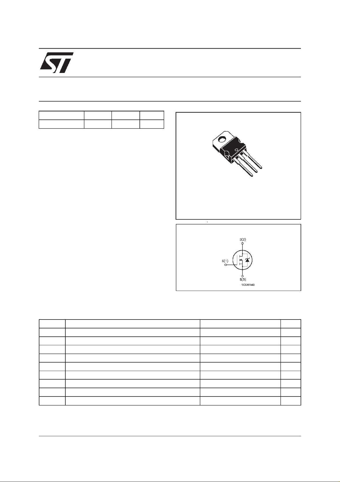
3
2
1
TO-220
INTERNAL SCHEMATIC DIAGRAM
ABSOLUTE MAXIMUM RATINGS
Symbol Parameter Value Unit
V
V
V
I
I
DM
P
T
(•) Pulse widthlimited by safeoperating area
First digit of the datecode being Zor K identifies silicon characterized in this datasheet.
July 1999
Dra in- sour c e Voltage ( VGS=0) 60 V
DS
Dra in- gate V ol t age (RGS=20kΩ)60V
DGR
Gat e-source Voltage
GS
I
Dra in Current (contin uous) at Tc=25oC12A
D
Dra in Current (pulsed) at Tc= 100oC9A
DM
20 V
±
(•) Dra in Current (pulsed) 48 A
Tot al Dissipation at Tc=25oC40W
tot
St orage Tem pe r at ur e -65 to 175
stg
T
Max. Operat ing Junc tion Tem perature 175
j
o
C
o
C
1/8
Page 2
MTP3055E
THERMAL DATA
R
thj-case
R
thj-amb
R
thc-s
T
AVALANCHE CHARACTERISTICS
Symbol Parameter Max Value Unit
I
AR
E
Ther mal Resistanc e Junct ion-case Max
Ther mal Resistanc e Junct ion-ambient Max
Ther mal Resistanc e Case-sink Ty p
Maximum L ead T emperat ure For Solder ing Purp os e
l
Avalanche Current, Repetitive or Not-Repetitive
(pulse width limited by T
Single Pulse A v alan che Ener gy
AS
(starting T
=25oC, ID=IAR,VDD=25V)
j
max)
j
3.75
62.5
0.5
300
12 A
50 mJ
o
C/W
oC/W
o
C/W
o
C
ELECTRICAL CHARACTERISTICS
=25oC unless otherwisespecified)
(T
case
OFF
Symbol Parameter Test Conditions Min. Typ. Max. Unit
V
(BR)DSS
Drain-source
ID=250µAVGS=0 60 V
Break dow n Volt age
I
DSS
I
GSS
Zero Gate Voltage
Drain Current (V
GS
Gat e- bod y Leakage
Current (V
DS
=0)
=0)
V
=MaxRating
DS
=MaxRatingx0.8 Tc=125oC
V
DS
V
=± 20 V
GS
1
10
100 nA
±
ON(∗)
Symbol Parameter Test Conditions Min. Typ. Max. Unit
V
GS(th)
R
DS(on)
Gate Threshold Voltage VDS=VGSID= 250 µA22.94V
Sta t ic Drain-sour c e On
VGS=10V ID=7A 0.1 0.15
Resistance
I
D(on)
On State Drain Current VDS>I
D(on)xRDS(on )maxVGS
=10V 12 A
DYNAMIC
Symbol Parameter Test Conditions Min. Typ. Max. Unit
g
(∗)Forward
fs
Tr ansc on duc tance
C
C
C
Input Capacitanc e
iss
Out put Capacitance
oss
Reverse Transfer
rss
Capacit a nc e
VDS>I
D(on)xRDS(on )maxID
=6A 4 6 S
VDS=25V f=1MHz VGS= 0 760
100
30
µ
µA
Ω
pF
pF
pF
A
2/8
Page 3
MTP3055E
ELECTRICAL CHARACTERISTICS
(continued)
SWITCHING RESISTIVE LOAD
Symbol Parameter Test Conditions Min. Typ. Max. Unit
t
d(on)
t
d(off)
Q
Q
Q
t
Turn-on Time
Rise T ime
r
Tur n-of f Delay Time
t
Fall T ime
f
Tot al Gate Charge
g
Gat e- Source Char g e
gs
Gate-Drain Charge
gd
VDD=30V ID=7A
R
G
=50
Ω
VGS=10V
(see t est circuit)
ID=12A VGS=10V
=40V
V
DD
(see t est circuit)
20
65
70
35
15
7
5
SOURCEDRAINDIODE
Symbol Parameter Test Conditions Min. Typ. Max. Unit
I
SD
I
SDM
V
SD
t
Q
(∗) Pulsed:Pulse duration = 300µs, duty cycle 1.5%
(•) Pulse width limited by safeoperating area
Source-drain Current
Source-drain Current
(•)
(pulsed)
12
48
(∗)ForwardOnVoltage ISD=12A VGS=0 2.0 V
Reverse Recovery
rr
Time
Reverse Recovery
rr
ISD= 12 A di/dt = 100 A/µs
=30V Tj= 150oC
V
DD
65
0.17
Charge
ns
ns
ns
ns
nC
nC
nC
A
A
ns
µ
C
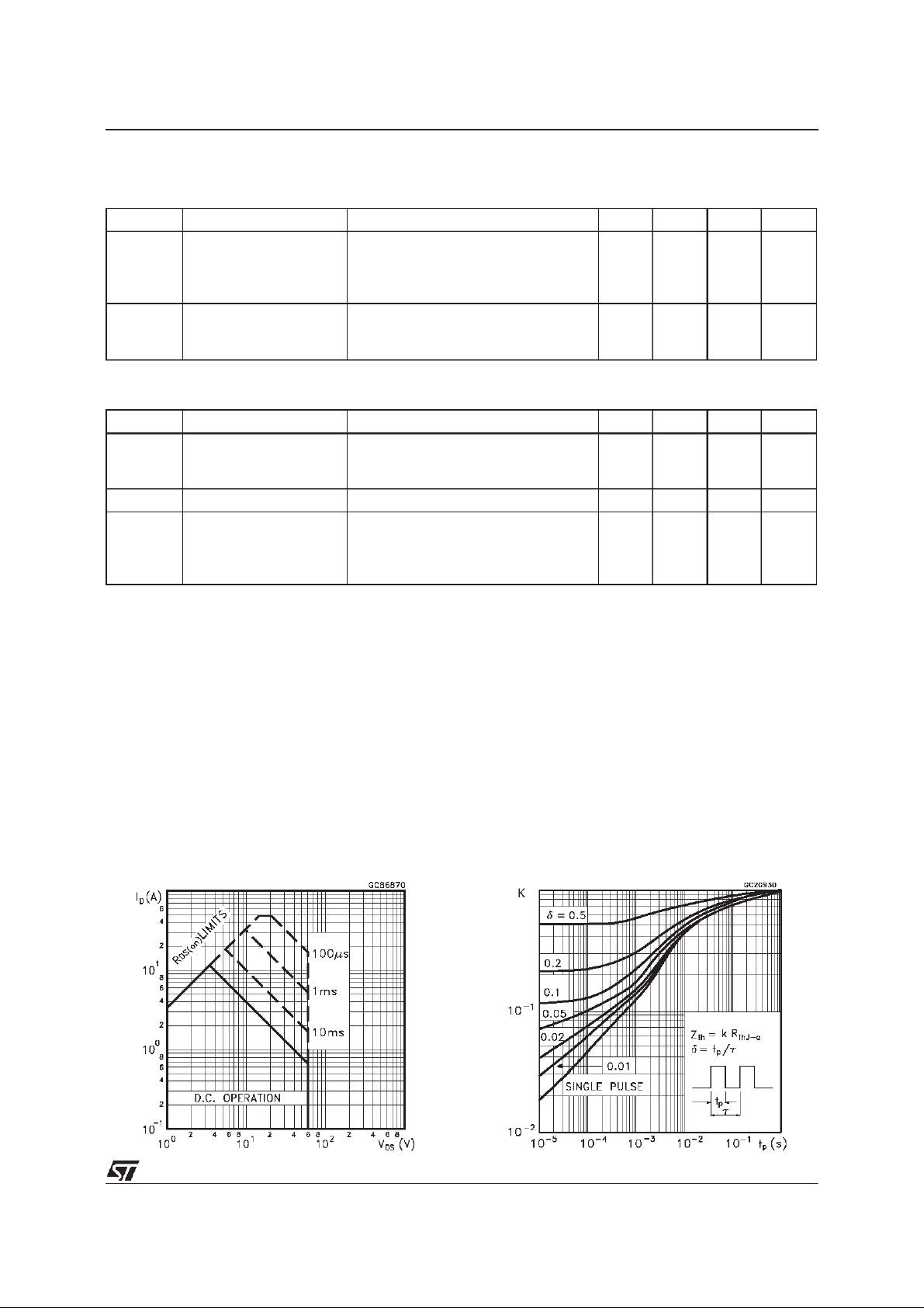
SafeOperating Area ThermalImpedance
3/8
Page 4

MTP3055E
OutputCharacteristics
Transconductance
TransferCharacteristics
Static Drain-sourceOn Resistance
Gate Charge vs Gate-sourceVoltage
4/8
CapacitanceVariations
Page 5

MTP3055E
NormalizedGate ThresholdVoltage vs
Temperature
Source-drainDiode Forward Characteristics
NormalizedOn Resistancevs Temperature
5/8
Page 6

MTP3055E
Fig. 1:
UnclampedInductiveLoad TestCircuit
Fig. 3: SwitchingTimes Test Circuits For
ResistiveLoad
Fig. 2:
UnclampedInductiveWaveform
Fig. 4: Gate Charge test Circuit
Fig. 5:
Test Circuit For InductiveLoad Switching
And Diode Recovery Times
6/8
Page 7

TO-220 MECHANICALDATA
MTP3055E
DIM.
MIN. TYP. MAX. MIN. TYP. MAX.
A 4.40 4.60 0.173 0.181
C 1.23 1.32 0.048 0.051
D 2.40 2.72 0.094 0.107
D1 1.27 0.050
E 0.49 0.70 0.019 0.027
F 0.61 0.88 0.024 0.034
F1 1.14 1.70 0.044 0.067
F2 1.14 1.70 0.044 0.067
G 4.95 5.15 0.194 0.203
G1 2.4 2.7 0.094 0.106
H2 10.0 10.40 0.393 0.409
L2 16.4 0.645
L4 13.0 14.0 0.511 0.551
L5 2.65 2.95 0.104 0.116
L6 15.25 15.75 0.600 0.620
L7 6.2 6.6 0.244 0.260
L9 3.5 3.93 0.137 0.154
DIA. 3.75 3.85 0.147 0.151
mm inch
E
A
L4
D
F2
F1
G1
H2
G
F
P011C
C
D1
L2
Dia.
L5
L7
L6
L9
7/8
Page 8

MTP3055E
Information furnished is believed to beaccurateand reliable.However, STMicroelectronics assumes no responsibilityfor the consequences
of use of such information nor for any infringement of patents or other rights of third parties which may result from its use. No license is
granted by implication or otherwise under anypatent or patent rights ofSTMicroelectronics. Specificationmentioned in this publicationare
subjecttochange withoutnotice.This publication supersedes andreplaces all informationpreviously supplied.STMicroelectronics products
are not authorized for use as critical components in lifesupportdevices or systems without express written approval of STMicroelectronics.
The STlogo is a trademark of STMicroelectronics
1999STMicroelectronics – Printed in Italy– All Rights Reserved
STMicroelectronics GROUP OF COMPANIES
Australia - Brazil - China- Finland - France - Germany - Hong Kong - India - Italy- Japan - Malaysia- Malta- Morocco-
8/8
Singapore - Spain - Sweden - Switzerland - United Kingdom- U.S.A.
http://www.st.com
.
 Loading...