

Page 1
CYStech Electronics Corp.
N-CHANNEL ENHANCEMENT MODE POWER MOSFET
Spec. No. : C805Q8
Issued Date : 2009.12.30
Revised Date :2011.03.21
Page No. : 1/9
MTNN20N03Q8
N-CH 1 N-CH 2
BVDSS 30V 60V
ID 8A 0.115A
Description
The MTNN20N03Q8 provides the designer with the best combination of fast switching, ruggedized device
design, low on-resistance and cost effectiveness.
The SOP-8 package is universally preferred for all commercial-industrial surface mount applications and
suited for low voltage applications such as DC/DC converters.
Features
Simple drive requirement
•
Low on-resistance
•
Fast switching speed
•
Two N-ch MOSFETs in a package
•
Pb-free lead plating package
•
RDSON(MAX)
20mΩ 5Ω
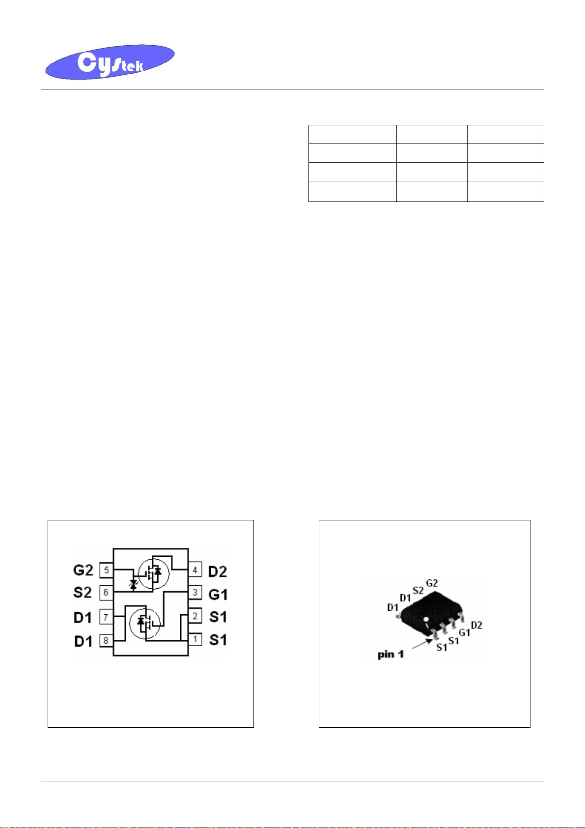
Equivalent Circuit Outline
MTNN20N03Q8 SOP-8
G:Gate
S:Source
D:Drain
MTNN20N03Q8 CYStek Product Specification
Page 2
CYStech Electronics Corp.
Absolute Maximum Ratings (Ta=25°C)
Spec. No. : C805Q8
Issued Date : 2009.12.30
Revised Date :2011.03.21
Page No. : 2/9
Parameter Symbol
Unit
N-CH 1 N-CH 2
Drain-Source Voltage VDS 30 60 V
Limits
Gate-Source Voltage VGS
D 8 0.115 A
Continuous Drain Current @ TC=25 °C (Note 1)
Continuous Drain Current @ TC=100 °C (Note 1)
I
I
D 6 0.08 A
±20 ±20
V
Pulsed Drain Current (Note 2&3) IDM 32 0.7 A
Total Power Dissipation @ TA=25 °C
Linear Derating Factor
ESD susceptibility (Note 4)
Operating Junction Temperature Tj -55~+150
Storage Temperature Tstg -55~+150
Thermal Resistance, Junction-to-Ambient (Note 1) Rth,ja 62.5
Note : 1. Surface mounted on 1 in² copper pad of FR-4 board; 135°C/W when mounted on minimum copper pad.
2. Pulse width limited by maximum junction temperature.
3. Pulse width≤300μs, duty cycle≤2%.
4. Human body model, 1.5kΩ in series with 100pF
Pd 2 0.4 W
0.016 0.016
1250 V
W / °C
°C
°C
°C/W
Characteristics (Tj=25°C, unless otherwise specified)
N-Channel MOSFET 1
Symbol Min. Typ. Max. Unit Test Conditions
Static
BV
30 - - V VGS=0, ID=250μA
DSS
V
1.0 1.5 3.0 V VDS = VGS, ID=250μA
GS(th)
GFS - 16 - S VDS =5V, ID=8A
I
- -
GSS
- - 1 VDS =24V, VGS =0
- - 25
- 15.5 20 VGS =10V, ID=8A
- 23 31
*R
I
DSS
DS(ON)
±
100
nA
μA
mΩ
VGS=±20
V
=20V, VGS =0, Tj=125°C
DS
V
=5V, ID=6A
GS
Dynamic
*Qg(VGS=10V) - 11 -
*Qg(VGS=5V) - 6 -
*Qgs - 1.2 -
nC I
=8A, VDS=15V, VGS=10V
D
*Qgd - 3.3 -
*td
- 11 -
(ON)
V
=15V, ID=1A,VGS=10V,
R
DS
=6Ω
G
*tr - 16 -
*td
- 36 -
(OFF)
ns
*tf - 20 -
Ciss - 1115 -
Coss - 116 -
pF V
=0V, VDS=15V, f=1MHz
GS
Crss - 82 -
Ω
Rg - 2 -
VGS=15mV, VDS=0V, f=1MHz
MTNN20N03Q8 CYStek Product Specification
Page 3
Spec. No. : C805Q8
CYStech Electronics Corp.
Issued Date : 2009.12.30
Revised Date :2011.03.21
Page No. : 3/9
Source-Drain Diode
*IS - - 2.3
*ISM - - 9.2
*VSD - - 1.2 V IF=I
*trr - 50 - ns
*Qrr - 2 - nC
A
S, VGS
, VGS=0, dI/dt=100A/μs
I
F=IS
=0V
N-Channel MOSFET 2
Symbol Min. Typ. Max. Unit Test Conditions
BV
V
R
60 - - V VGS=0, ID=10μA
DSS*
1 - 2.5 V VDS=VGS, ID=250μA
GS(th)
I
- - ±10 μA VGS=±20V, VDS=0
GSS
I
- - 1 μA VDS=60V, VGS=0
DSS
DS(ON)*
- 3.6 5.5 ID=100mA, VGS=5V
- 3 5
Ω
ID=100mA, VGS=10V
GFS 100 - - mS VDS=10V, ID=100mA
C
- 30.5 -
iss
C
- 9.3 -
oss
C
- 5.9 -
rss
pF VDS=10V, VGS=0, f=1MHz
*Pulse Test : Pulse Width ≤300μs, Duty Cycle≤2%
Ordering Information
Device Package Shipping
MTNN20N03Q8
(Pb-free lead plating package)
SOP-8
3000 pcs / Tape & Reel
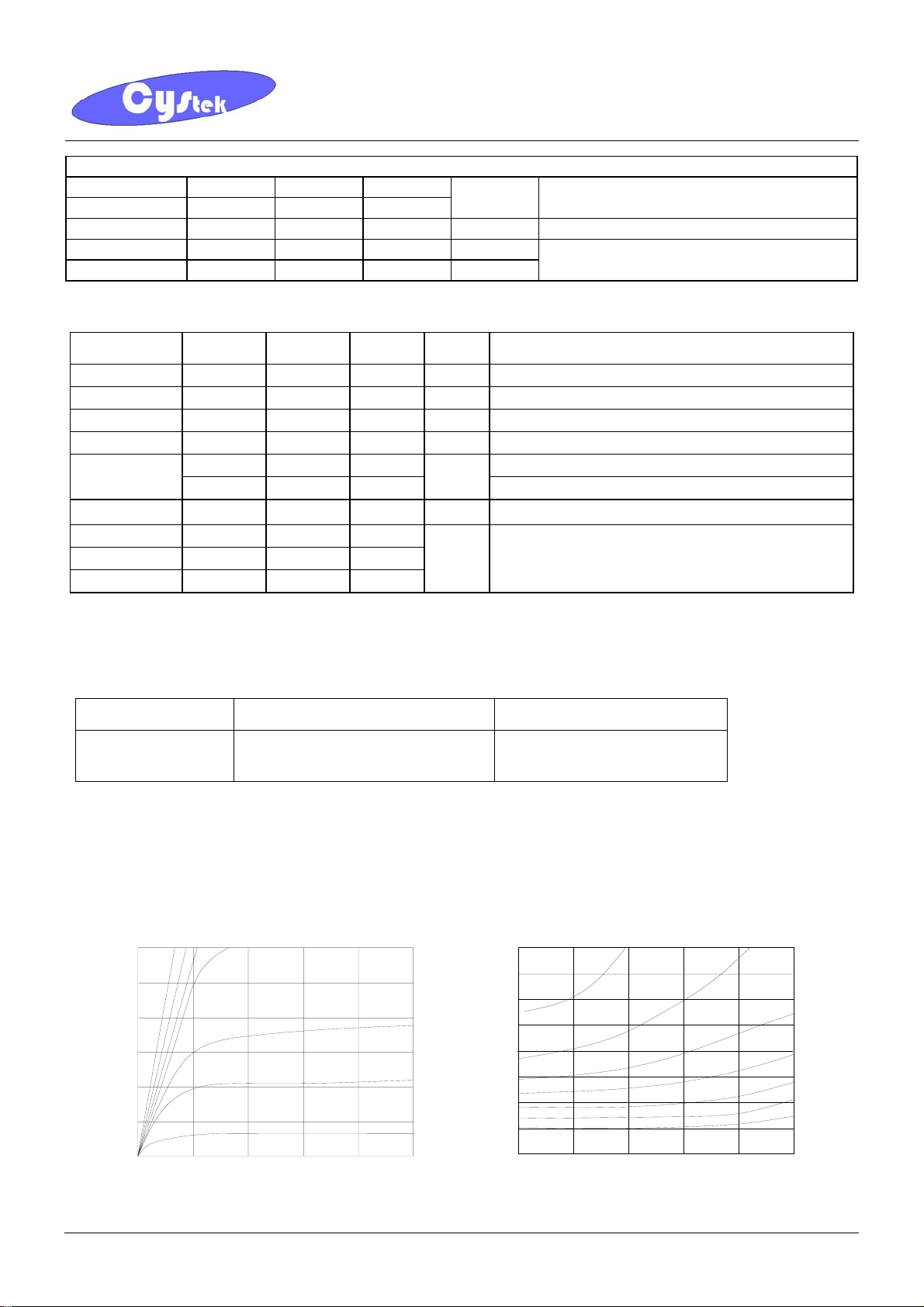
Typical Characteristics
N-CH MOSFET 1
30
V = 10 V
GS
25
20
15
10
D
I - Drain Current (A)
5
0
0
On-Region Charact eri sti cs
6V
7V
5V
12
V - Dr ain Source Voltage(V)
DS
4.5V
4V
3.5V
3
4
5
On-Resistance Vari ation wi th Drain Cur rent and Gat e Volt age
2.4
2.2
V = 3. 5 V
GS
2.0
1.8
1.6
1.4
DS(ON)
1.2
1.0
R -Normalized
Drain-Source On-Resist ance
0.8
0
4.0 V
4.5 V
6
12
I - Drain Curr ent (A)
D
5.0 V
6.0 V
7.0 V
18 24
10 V
30
MTNN20N03Q8 CYStek Product Specification
Page 4

Spec. No. : C805Q8
CYStech Electronics Corp.
Issued Date : 2009.12.30
Revised Date :2011.03.21
Page No. : 4/9
On-Resi stance Variat ion w ith Temperat ure
1.9
I = 8A
D
V = 10V
GS
1.6
On-Resist ance Variation wit h Gate-to-Source Volt age
0.09
I = 8 A
0.08
0.07
D
DS(ON)
R - On-Resistance( Ω )
0.06
0.05
0.04
0.03
0.02
0.01
T = 125° C
A
T = 25° C
A
2
4
V - Gat e-Source Vol t age( V )
6
GS
810
1.3
1.0
DS(on)
R - Nor malized
Drain-Source On-Resistance
0.7
0.4
-50
0
-25 25
T - Juncti on Temperature (° C)
J
75
100 150
12550
30
25
20
15
10
D
I - Drain Current (A)
5
V = 10V
DS
Transf er Charact er ist ics
T = -55° C
A
125° C
25° C
Is - Reverse Drain Current( A )
100
10
0.1
0.01
Body Diode Forw ard Volt age Variation
wit h Source Current and Temperature
V = 0V
GS
T = 1 25° C
A
1
25° C
-55° C
0
1
1.5
GS
V - Gat e-Sou rce Volt age( V )
2.0
3.02.5 3.5
0.001
0.2 0.6
0
0.4
V - Body Diode Forward Volt age( V )
SD
1.00.8 1.2
1.4
10
8
6
4
GS
V - Gat e-Sour ce Volt age( V )
2
0
Gate Char ge Ch aract erist ics
I = 8A
D
0
Q - Gate Charge( nC )
g
V = 5V
DS
48
10V
15V
12 16
Capacit ance(pF)
1500
1350
1200
1050
900
750
600
450
300
150
Cap a ci t an c e Ch a r ac t er i st i c s
0
5
0
V - Dr ain -Sou rce Vo lt age( V )
DS
f = 1MHz
V = 0 V
GS
Ci s s
Co s s
Cr s s
15
10
20
25 30
MTNN20N03Q8 CYStek Product Specification
Page 5

100
10
D
0.1
I - Drain Current ( A )
0.01
0.1
Maximum Safe Operating Ar ea
R Li mit
DS(ON)
1
V = 10V
GS
Si n gl e Pu l se
R = 125°C/W
θJA
T = 25°C
A
1
V - Dr ain-Sour ce Vol ta ge( V )
DS
N-CH MOSFET 2
CYStech Electronics Corp.
Single Pulse Maximum Power Dissipation
DC
10s
1ms
10ms
100ms
1s
10 100
100
μs
50
40
30
20
10
P( pk ),Peak Transi ent Po wer ( W )
0
0.001 0.01 0.1 10010
Spec. No. : C805Q8
Issued Date : 2009.12.30
Revised Date :2011.03.21
Page No. : 5/9
Si n gl e Pu l se
R = 125° C/ W
θJA
T = 25° C
A
1
1000
Drain Curre nt - ID(A)
Typical Output Characteristics
0.3
0.25
0.2
0.15
0.1
0.05
6V
0
01234
Static Drain-Source On-State resistance vs Drain Current
10
4V
3.5V
3V
VGS= 2.2V
Drain-Source Voltage -VDS(V)
VGS=5V
Typical Transfer Characteristics
0.3
0.25
0.2
0.15
0.1
Drain Current -ID(A)
0.05
0
01234
10
VDS= 10V
Gate-Source Voltage-VGS(V)
St at ic Dra in-Source On-St at e res istance vs Drai n C urre nt
Resistance-RDS(on)(Ω)
Static Drain-Source On-State
1
0.01 0.1 1
Drain Current-ID(A)
Resistance-RDS(on)(Ω)
Static Drain-Source On-State
1
0.01 0.1 1
VGS= 10V
Drain C urrent-ID(A)
MTNN20N03Q8 CYStek Product Specification
Page 6

Spec. No. : C805Q8
CYStech Electronics Corp.
Issued Date : 2009.12.30
Revised Date :2011.03.21
Page No. : 6/9
Static Drain-Source On-State Resistance vs Gate-Source
Voltage
7
6
5
10
Reverse Drain Current vs Source-Drain Voltage
1
4
3
2
Resistance-RDS(ON)(Ω)
Static Drain-Source On-State
1
0
0 5 10 15 20 25
ID=50mA
ID=100mA
Gate-Source Voltage-VGS(V)
0.1
0.01
Source-Drain Voltage-VSD(V)
0.001
0 0.2 0.4 0.6 0.8 1
Reverse Drain Current -IDR(A)
Capacitance vs Drain-to-Source Voltage
100
Ciss
C
10
Capacitance---(pF)
oss
Crss
1
0.1 1 10 100
Drain-Source Voltage -VDS(V)
MTNN20N03Q8 CYStek Product Specification
Page 7

Reel Dimension
CYStech Electronics Corp.
Spec. No. : C805Q8
Issued Date : 2009.12.30
Revised Date :2011.03.21
Page No. : 7/9
Carrier Tape Dimension
MTNN20N03Q8 CYStek Product Specification
Page 8

CYStech Electronics Corp.
Recommended wave soldering condition
Product Peak Temperature Soldering Time
Pb-free devices
Recommended temperature profile for IR reflow
260 +0/-5 °C
Spec. No. : C805Q8
Issued Date : 2009.12.30
Revised Date :2011.03.21
Page No. : 8/9
5 +1/-1 seconds
Profile feature Sn-Pb eutectic Assembly
Average ramp-up rate
(Tsmax to Tp)
Preheat
−Temperature Min(TS min)
−Temperature Max(TS max)
−Time(ts min to ts max)
Time maintained above:
−Temperature (TL)
− Time (tL)
Peak Temperature(TP)
Time within 5°C of actual peak
temperature(tp)
Ramp down rate
Time 25 °C to peak temperature
Note : All temperatures refer to topside of the package, measured on the package body surface.
MTNN20N03Q8 CYStek Product Specification
3°C/second max. 3°C/second max.
100°C
150°C
60-120 seconds
183°C
60-150 seconds
240 +0/-5 °C 260 +0/-5 °C
10-30 seconds 20-40 seconds
6°C/second max. 6°C/second max.
6 minutes max. 8 minutes max.
Pb-free Assembly
150°C
200°C
60-180 seconds
217°C
60-150 seconds
Page 9

g
SOP-8 Dimension
CYStech Electronics Corp.
Spec. No. : C805Q8
Issued Date : 2009.12.30
Revised Date :2011.03.21
Page No. : 9/9
Top View
B
A
C
Right side View
G
I
H
Device Name
Date Code
Marking:
20N03
□□□□
J
E
DIM
D
Front View
Part A
F
Inches Millimeters Inches Millimeters
Min. Max. Min. Max.
A 0.1890 0.2007 4.80 5.10 I 0.0098 REF 0.25 REF
B 0.1496 0.1654 3.80 4.20 J 0.0118 0.0354 0.30 0.90
C 0.2283 0.2441 5.80 6.20 K 0.0074 0.0098 0.19 0.25
D 0.0480 0.0519 1.22 1.32 L 0.0145 0.0204 0.37 0.52
E 0.0138 0.0193 0.35 0.49 M 0.0118 0.0197 0.30 0.50
F 0.1472 0.1527 3.74 3.88 N 0.0031 0.0051 0.08 0.13
G 0.0531 0.0689 1.35 1.75 O 0.0000 0.0059 0.00 0.15
H 0.1889 0.2007 4.80 5.10
Notes: 1.Controlling dimension: millimeters.
Material:
• Lead: Pure tin plated.
• Mold Compound: Epoxy resin family, flammability solid burning class: UL94V-0.
2.Maximum lead thickness includes lead finish thickness, and minimum lead thickness is the minimum thickness of base material.
3.If there is any question with packing specification or packing method, please contact your local CYStek sales office.
Part A
M
K
L
N
O
DIM
Min. Max. Min. Max.
8-Lead SOP-8 Plastic Package
CYStek Packa
e Code: Q8
*: Typical
Important Notice:
• All rights are reserved. Reproduction in whole or in part is prohibited without the prior written approval of CYStek.
• CYStek reserves the right to make changes to its products without notice.
• CYStek semiconductor products are not warranted to be suitable for use in Life-Support Applications, or systems.
• CYStek assumes no liability for any consequence of customer product design, infringement of patents, or application assistance.
MTNN20N03Q8 CYStek Product Specification
Page 10

 Loading...