

Page 1
CYStech Electronics Corp.
20V N-CHANNEL Enhancement Mode MOSFET
MTN2302N3
Features
VDS=20V
•
R
R
Advanced trench process technology
•
High density cell design for ultra low on resistance
•
Excellent thermal and electrical capabilities
•
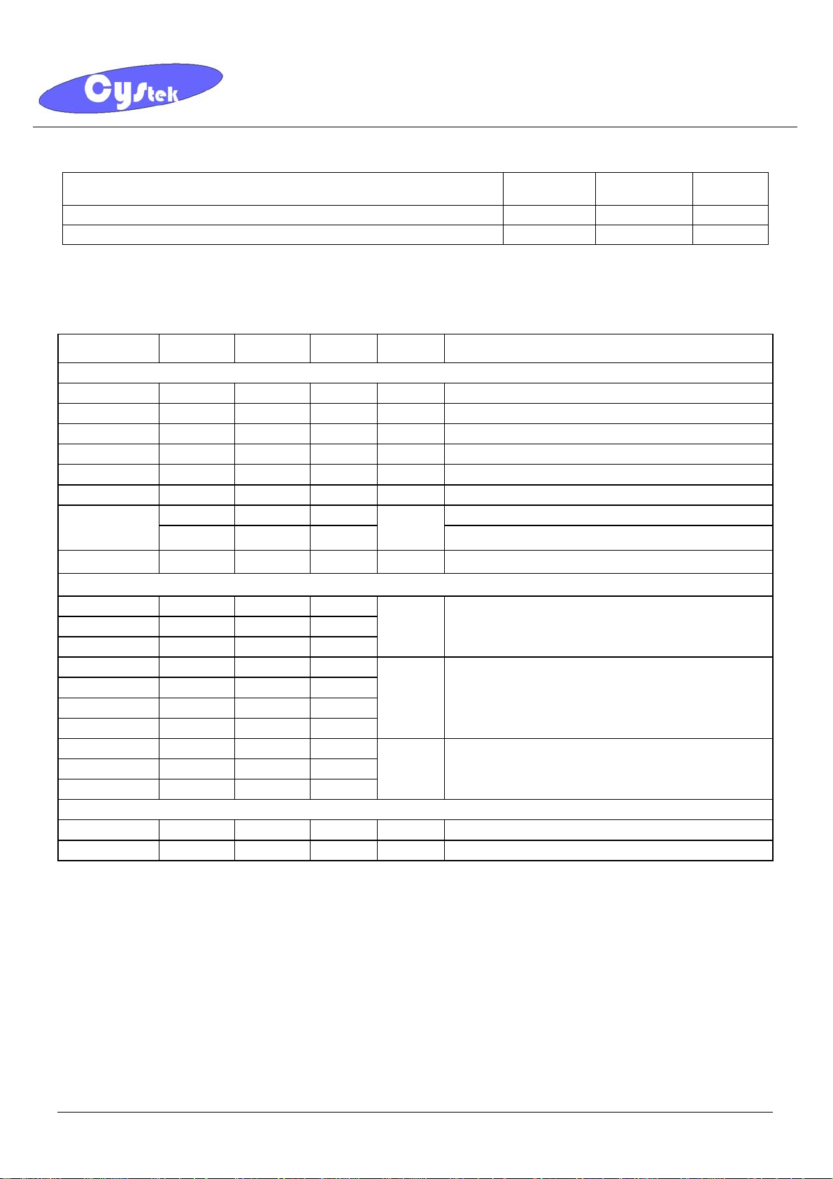
Compact and low profile SOT-23 package
•
=65mΩ@VGS=4.5V, IDS=3.6A
DS(ON)
=95mΩ@VGS=2.5V, IDS=3.1A
DS(ON)
Spec. No. : C323N3
Issued Date : 2004.04.05
Revised Date : 2004.10.22 . .
Page No. : 1/5
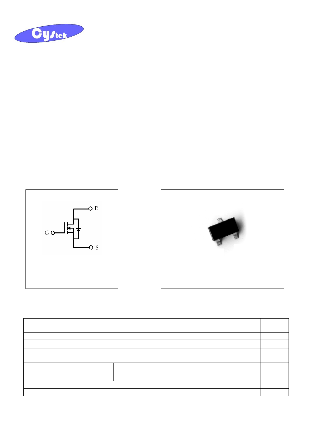
Equivalent Circuit Outline
MTN2302N3
G:Gate
S:Source
D:Drain
Absolute Maximum Ratings (Ta=25°C)
Parameter Symbol Limits Unit
SOT-23
D
S
G
Drain-Source Voltage VDS 20 V
Gate-Source Voltage VGS ±8 V
Continuous Drain Current ID 2.4 A
Pulsed Drain Current IDM 10 A
Maximum Power Dissipation
Operating Junction Temperature Tj -55~+150
Storage Temperature Tstg -55~+150
MTN2302N3 CYStek Product Specification
Ta=25℃
Ta=75℃
P
D
1.25
W
0.8
°C
°C
Page 2
Thermal Performance
Parameter Symbol Limit Unit
CYStech Electronics Corp.
Spec. No. : C323N3
Issued Date : 2004.04.05
Revised Date : 2004.10.22 . .
Page No. : 2/5
Thermal Resistance, Junction-to-Ambient(PCB mounted) Rth,ja 100
Lead Temperature, for 5 second Soldering(1/8” from case) TL 260
Note : Surface mounted on FR-4 board, t≦5sec.
Electrical Characteristics (Ta=25°C)
Symbol Min. Typ. Max. Unit Test Conditions
Static
BV
V
*I
20 - - V VGS=0, ID=250µA
DSS
0.45 - - V VDS=VGS, ID=250µA
GS(th)
I
- - 100 nA VGS=+8V, VDS=0
GSS/F
I
- - -100 nA VGS=-8V, VDS=0
GSS/R
I
- - 1 µA VDS=20V, VGS=0
DSS
6 - - A VDS=5V, VGS=4.5V
D(ON)
- 50 65 ID=3.6A, VGS=4.5V
*R
DS(ON)
- 75 95
mΩ
ID=3.1A, VGS=2.5V
*GFS - 10 - S VDS=5V, ID=3.6A
Dynamic
Ciss - 450 -
Coss - 70 -
pF VDS=10V, VGS=0, f=1MHz
Crss - 43 -
t
- 7 15
d(ON)
V
=10V, ID=1A, RL=10Ω
tr - 55 80
t
- 16 60
d(OFF)
ns
DD
V
=4.5V, RG=6Ω
GEN
tf - 10 25
Qg - 5.2 10
Qgs - 0.65 -
nC
Qgd - 1.5 -
VDS=10V, ID=3.6A,
V
=4.5V,
GS
Source-Drain Diode
ISD - - 1.6 A -
VSD - 0.75 1.2 V VGS=0V, ISD=1A
*Pulse Test : Pulse Width ≤300µs, Duty Cycle≤2%
°C/W
°C
MTN2302N3 CYStek Product Specification
Page 3

CYStech Electronics Corp.
Characteristic Curves
Spec. No. : C323N3
Issued Date : 2004.04.05
Revised Date : 2004.10.22 . .
Page No. : 3/5
MTN2302N3 CYStek Product Specification
Page 4

Spec. No. : C323N3
CYStech Electronics Corp.
Issued Date : 2004.04.05
Revised Date : 2004.10.22 . .
Page No. : 4/5
MTN2302N3 CYStek Product Specification
Page 5

SOT-23 Dimension
A
CYStech Electronics Corp.
L
Spec. No. : C323N3
Issued Date : 2004.04.05
Revised Date : 2004.10.22 . .
Page No. : 5/5
Marking:
C
DIM
3
S
B
1
V
D
G
2
H
K
Inches Millimeters Inches Millimeters
Min. Max. Min. Max.
J
DIM
Surface Mounted Package
CYStek Package Code: N3
Style: Pin 1.Gate 2.Source 3.Drain
Min. Max. Min. Max.
02
3-Lead SOT-23 Plastic
A 0.1102 0.1204 2.80 3.04 J 0.0034 0.0070 0.085 0.177
B 0.0472 0.0630 1.20 1.60 K 0.0128 0.0266 0.32 0.67
C 0.0335 0.0512 0.89 1.30 L 0.0335 0.0453 0.85 1.15
D 0.0118 0.0197 0.30 0.50 S 0.0830 0.1083 2.10 2.75
G 0.0669 0.0910 1.70 2.30 V 0.0098 0.0256 0.25 0.65
H 0.0005 0.0040 0.013 0.10
Notes: 1.Controlling dimension: millimeters.
Material:
• Lead: 42 Alloy ; solder plating
• Mold Compound: Epoxy resin family, flammability solid burning class: UL94V-0
2.Maximum lead thickness includes lead finish thickness, and minimum lead thickness is the minimum thickness of base material.
3.If there is any question with packing specification or packing method, please contact your local CYStek sales office.
Important Notice:
• All rights are reserved. Reproduction in whole or in part is prohibited without the prior written approval of CYStek.
• CYStek reserves the right to make changes to its products without notice.
• CYStek semiconductor products are not warranted to be suitable for use in Life-Support Applications, or systems.
• CYStek assumes no liability for any consequence of customer product design, infringement of patents, or application assistance.
TE
*: Typical
MTN2302N3 CYStek Product Specification
Page 6

 Loading...