

Page 1
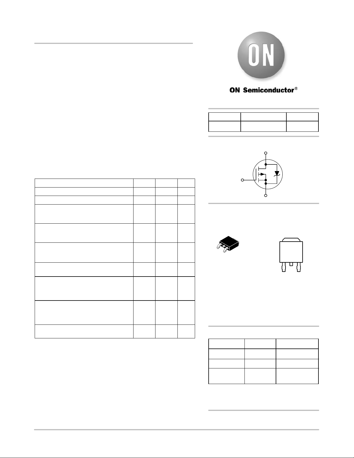
MTD5P06V
)
l
l
s
Preferred Device
Power MOSFET
5 Amps, 60 Volts P−Channel DPAK
This Power MOSFET is designed to withstand high energy in the
avalanche and commutation modes. Designed for low voltage, high
speed switching applications in power supplies, converters and power
motor controls, these devices are particularly well suited for bridge
circuits where diode speed and commutating safe operating areas are
critical and offer additional safety margin against unexpected voltage
transients.
Features
• Avalanche Energy Specified
• I
and V
DSS
• Pb−Free Packages are Available
Specified at Elevated Temperature
DS(on)
(BR)DSS
60 V
http://onsemi.com
R
TYP
DS(on)
340 mW
P−Channel
D
ID MAXV
5.0 A
MAXIMUM RATINGS (T
Rating Symbol Value Unit
Drain−to−Source Voltage V
Drain−to−Gate Voltage (RGS = 1.0 MW)
Gate−to−Source Voltage
− Continuous
− Non−repetitive (tp ≤ 10 ms)
Drain Current − Continuous @ 25°C
− Continuous @ 100°C
− Single Pulse (tp ≤ 10 ms)
Total Power Dissipation @ 25°C
Derate above 25°C
Total Power Dissipation @ TA = 25°C (Note 2
Operating and Storage Temperature Range TJ, T
Single Pulse Drain−to−Source Avalanche
Energy − Starting TJ = 25°C
(VDD = 25 Vdc, VGS = 10 Vdc, Peak
IL = 5 Apk, L = 10 mH, RG = 25 W)
Thermal Resistance
Junction−to−Case
Junction−to−Ambient (Note 1)
Junction−to−Ambient (Note 2)
Maximum Lead Temperature for Soldering
Purposes, 1/8″ from Case for 10 seconds
Stresses exceeding Maximum Ratings may damage the device. Maximum
Ratings are stress ratings only. Functional operation above the Recommended
Operating Conditions is not implied. Extended exposure to stresses above the
Recommended Operating Conditions may affect device reliability.
1. When surface mounted to an FR4 board using the minimum recommended
pad size.
2. When surface mounted to an FR−4 board using the 0.5 sq in drain pad size.
= 25°C unless otherwise noted)
C
DSS
V
DGR
V
GS
V
GSM
I
D
I
D
I
DM
P
D
stg
E
AS
R
q
JC
R
q
JA
R
q
JA
T
L
60 Vdc
60 Vdc
± 15
± 25
5
4
18
40
0.27
2.1
− 55 to
175
125 mJ
3.75
100
71.4
260 °C
Vdc
Vpk
Adc
Apk
W
W/°C
W
°C
°C/W
G
S
MARKING
DIAGRAM
4
1
Gate
Drain
YWW5P06VG
2
3
Drain
Source
4
2
1
3
DPAK
CASE 369C
STYLE 2
Y = Year
WW = Work Week
5P06V = Device Code
G = Pb−Free Package
ORDERING INFORMATION
Device Package Shipping
MTD5P06V DPAK 75 Units/Rail
MTD5P06VT4 DPAK 2500/Tape & Ree
MTD5P06VT4G DPAK
(Pb−Free)
2500/Tape & Ree
†
© Semiconductor Components Industries, LLC, 2006
July, 2006 − Rev. 6
†For information on tape and reel specifications,
including part orientation and tape sizes, please
refer to our Tape and Reel Packaging Specification
Brochure, BRD8011/D.
Preferred devices are recommended choices for future use
and best overall value.
1 Publication Order Number:
MTD5P06V/D
Page 2
MTD5P06V
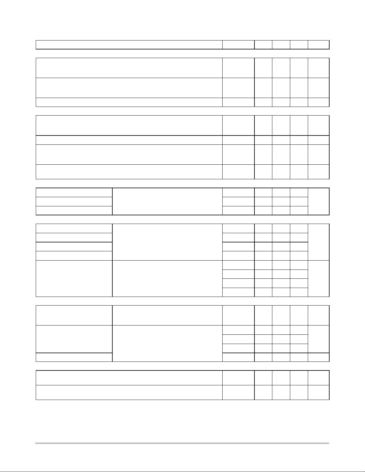
ELECTRICAL CHARACTERISTICS (T
= 25°C unless otherwise noted)
J
Characteristic Symbol Min Typ Max Unit
OFF CHARACTERISTICS
Drain−Source Breakdown Voltage
(VGS = 0 Vdc, ID = 0.25 mAdc)
V
(BR)DSS
Temperature Coefficient (Positive)
Zero Gate Voltage Drain Current
(VDS = 60 Vdc, VGS = 0 Vdc)
(VDS = 60 Vdc, VGS = 0 Vdc, TJ = 150°C)
Gate−Body Leakage Current (VGS = ± 15 Vdc, VDS = 0 Vdc) I
ON CHARACTERISTICS (Note 3)
Gate Threshold Voltage
V
(VDS = VGS, ID = 250 mAdc)
Threshold Temperature Coefficient (Negative)
Static Drain−Source On−Resistance (VGS = 10 Vdc, ID = 2.5 Adc) R
Drain−Source On−Voltage
V
(VGS = 10 Vdc, ID = 5 Adc)
(VGS = 10 Vdc, ID = 2.5 Adc, TJ = 150°C)
Forward Transconductance
(VDS = 15 Vdc, ID = 2.5 Adc)
DYNAMIC CHARACTERISTICS
Input Capacitance
Output Capacitance C
(VDS = 25 Vdc, VGS = 0 Vdc,
f = 1.0 MHz)
Transfer Capacitance C
SWITCHING CHARACTERISTICS (Note 4)
Turn−On Delay Time
Rise Time t
Turn−Off Delay Time t
(V
= 30 Vdc, ID = 5 Adc,
DD
VGS = 10 Vdc, RG = 9.1 W)
Fall Time t
Gate Charge
(See Figure 8)
(VDS = 48 Vdc, ID = 5 Adc, VGS = 10 Vdc)
SOURCE−DRAIN DIODE CHARACTERISTICS
Forward On−Voltage
(IS = 5 Adc, VGS = 0 Vdc)
(IS = 5 Adc, VGS = 0 Vdc, TJ = 150°C)
Reverse Recovery Time
(IS = 5 Adc, VGS = 0 Vdc,
dIS/dt = 100 A/ms)
Reverse Recovery Stored Charge Q
INTERNAL PACKAGE INDUCTANCE
Internal Drain Inductance
(Measured from the drain lead 0.25″ from package to center of die)
Internal Source Inductance
(Measured from the source lead 0.25″ from package to source bond pad)
I
DSS
GSS
GS(th)
DS(on)
DS(on)
g
FS
C
iss
oss
rss
t
d(on)
r
d(off)
f
Q
T
Q
1
Q
2
Q
3
V
SD
t
rr
t
a
t
b
RR
L
D
L
S
60
Vdc
−−61.2−−
mV/°C
mAdc
−
−
−
10
−
100
− − 100 nAdc
Vdc
2.0−2.8
4.7
4.0
−
mV/°C
− 0.34 0.45
Vdc
−
−
−
2.7
−
2.6
Mhos
1.5 3.6 −
− 367 510 pF
− 140 200
− 29 60
− 11 20 ns
− 26 50
− 17 30
− 19 40
− 12 20 nC
− 3.0 −
− 5.0 −
− 5.0 −
Vdc
−−1.72
1.34
3.5
−
− 97 −
− 73 −
− 24 −
− 0.42 −
− 4.5 −
− 7.5 −
W
ns
mC
nH
nH
3. Pulse Test: Pulse Width ≤ 300 ms, Duty Cycle ≤ 2%.
4. Switching characteristics are independent of operating junction temperature.
http://onsemi.com
2
Page 3
MTD5P06V
TYPICAL ELECTRICAL CHARACTERISTICS
10
8
6
4
, DRAIN CURRENT (AMPS)
D
I
2
0
012345
VGS = 10V
T
= 25°C
J
VDS, DRAIN−TO−SOURCE VOLTAGE (VOLTS)
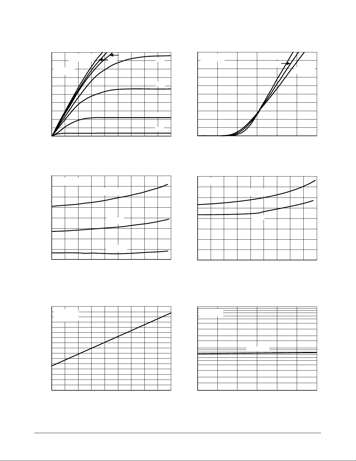
Figure 1. On−Region Characteristics
0.6
VGS = 10 V
0.55
0.5
0.45
0.4
0.35
9 V
T
= 100°C
J
25°C
8 V
10
7 V
6 V
5 V
4 V
7
6
89
VDS ≥ 10 V
9
8
7
6
5
4
3
, DRAIN CURRENT (AMPS)
D
I
2
1
0
23 4 8
VGS, GATE−TO−SOURCE VOLTAGE (VOLTS)
T
= −55°C
J
25°C
100°C
567
Figure 2. Transfer Characteristics
0.4
T
= 25°C
J
0.35
0.3
VGS = 10 V
15 V
0.3
, DRAIN−TO−SOURCE RESISTANCE (OHMS)
0.25
DS(on)
0.2
R
123456
ID, DRAIN CURRENT (AMPS)
−55°C
7
Figure 3. On−Resistance versus Drain Current
and Temperature
1.8
VGS = 10 V
1.6
ID = 2.5 A
1.4
1.2
1
0.8
(NORMALIZED)
0.6
, DRAIN−TO−SOURCE RESISTANCE
0.4
DS(on)
R
0.2
−50
−25 0 25 50 75 100 150
TJ, JUNCTION TEMPERATURE (°C)
8910
125
175
0.25
, DRAIN−TO−SOURCE RESISTANCE (OHMS)
DS(on)
0.2
R
12345 7
ID, DRAIN CURRENT (AMPS)
Figure 4. On−Resistance versus Drain Current
and Gate Voltage
100
VGS = 0 V
10
, LEAKAGE (nA)
DSS
I
1
010203040
VDS, DRAIN−TO−SOURCE VOLTAGE (VOLTS)
TJ = 125°C
8
96
10
50
60
Figure 5. On−Resistance Variation with
Temperature
http://onsemi.com
Figure 6. Drain−To−Source Leakage
Current versus Voltage
3
Page 4
MTD5P06V
POWER MOSFET SWITCHING
Switching behavior is most easily modeled and predicted
by recognizing that the power MOSFET is charge
controlled. The lengths of various switching intervals (Dt)
are determined by how fast the FET input capacitance can
be charged by current from the generator.
The published capacitance data is difficult to use for
calculating rise and fall because drain−gate capacitance
varies greatly with applied voltage. Accordingly, gate
charge data is used. In most cases, a satisfactory estimate of
average input current (I
) can be made from a
G(AV)
rudimentary analysis of the drive circuit so that
t = Q/I
G(AV)
During the rise and fall time interval when switching a
resistive load, VGS remains virtually constant at a level
known as the plateau voltage, V
. Therefore, rise and fall
SGP
times may be approximated by the following:
tr = Q2 x RG/(VGG − V
tf = Q2 x RG/V
GSP
GSP
)
where
VGG = the gate drive voltage, which varies from zero to V
GG
RG = the gate drive resistance
and Q2 and V
are read from the gate charge curve.
GSP
During the turn−on and turn−off delay times, gate current is
not constant. The simplest calculation uses appropriate
values from the capacitance curves in a standard equation for
voltage change in an RC network. The equations are:
t
d(on)
t
d(off)
= RG C
= RG C
In [VGG/(V
iss
In (VGG/V
iss
GG
GSP
− V
)
GSP
)]
The capacitance (C
) is read from the capacitance curve at
iss
a voltage corresponding to the off−state condition when
calculating t
on−state when calculating t
and is read at a voltage corresponding to the
d(on)
.
d(off)
At high switching speeds, parasitic circuit elements
complicate the analysis. The inductance of the MOSFET
source lead, inside the package and in the circuit wiring
which is common to both the drain and gate current paths,
produces a voltage at the source which reduces the gate drive
current. The voltage is determined by Ldi/dt, but since di/dt
is a function of drain current, the mathematical solution is
complex. The MOSFET output capacitance also
complicates the mathematics. And finally, MOSFETs have
finite internal gate resistance which effectively adds to the
resistance of the driving source, but the internal resistance
is difficult to measure and, consequently, is not specified.
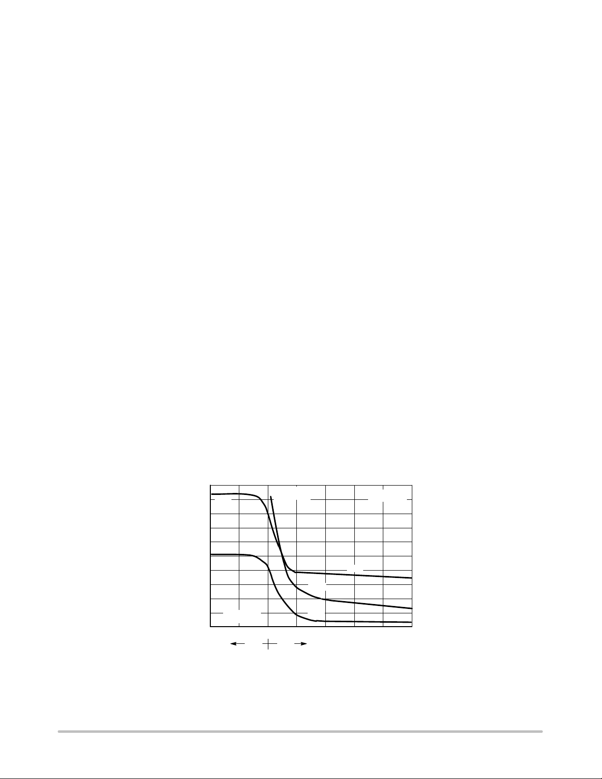
The resistive switching time variation versus gate
resistance (Figure 9) shows how typical switching
performance is affected by the parasitic circuit elements. If
the parasitics were not present, the slope of the curves would
maintain a value of unity regardless of the switching speed.
The circuit used to obtain the data is constructed to minimize
common inductance in the drain and gate circuit loops and
is believed readily achievable with board mounted
components. Most power electronic loads are inductive; the
data in the figure is taken with a resistive load, which
approximates an optimally snubbed inductive load. Power
MOSFETs may be safely operated into an inductive load;
however, snubbing reduces switching losses.
1000
C
900
iss
800
700
600
C
rss
500
400
300
C, CAPACITANCE (pF)
200
100
VGS = 0 V
0
10 0 5 10 15
5
V
GATE−TO−SOURCE OR DRAIN−TO−SOURCE VOLTAGE (VOLTS)
Figure 7. Capacitance Variation
VDS = 0 V
V
GS
DS
http://onsemi.com
4
T
= 25°C
J
C
iss
C
oss
C
rss
20 25
Page 5
MTD5P06V
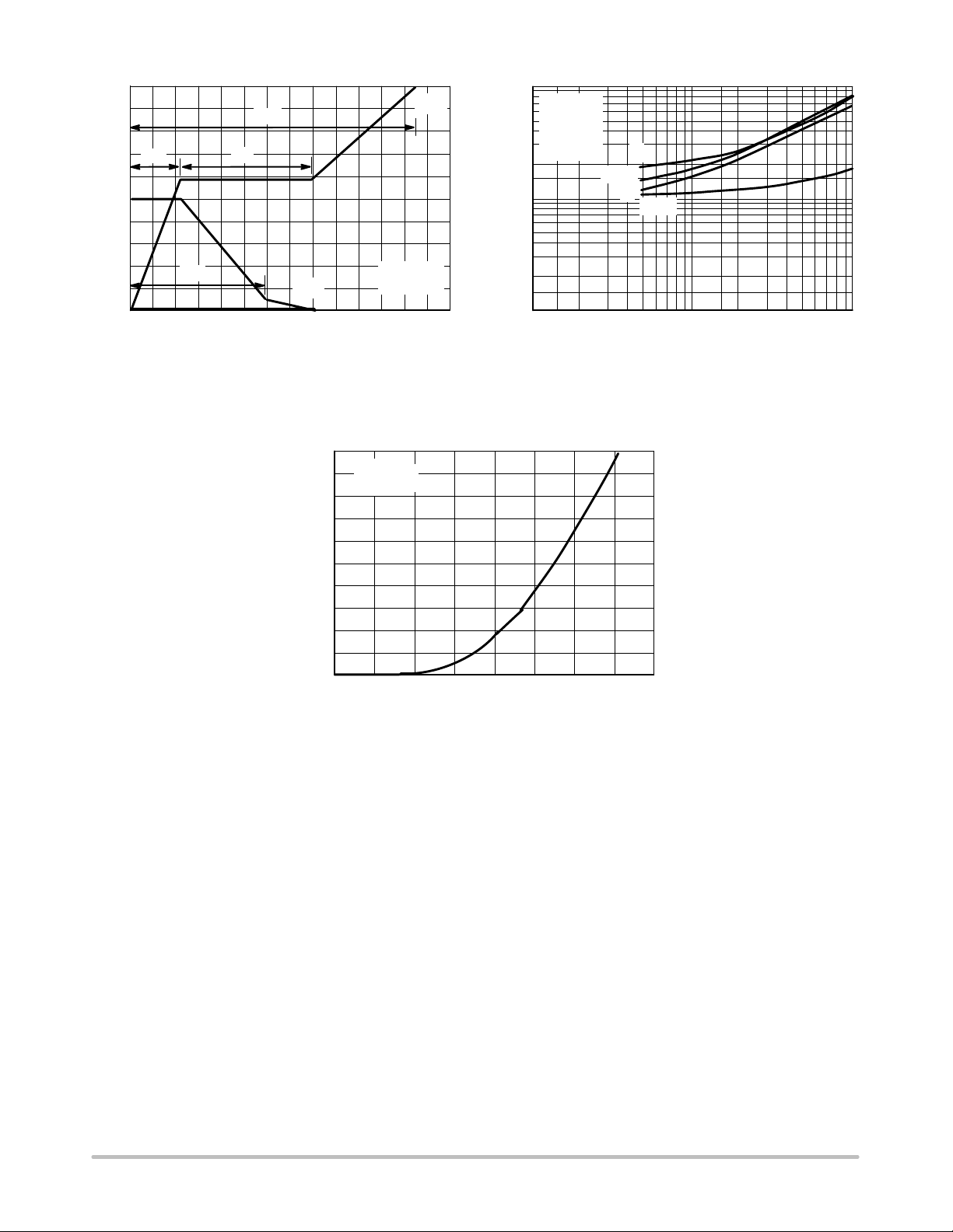
10
, GATE−TO−SOURCE VOLTAGE (VOLTS)
GS
V
9
8
7
Q1
6
5
4
3
2
1
0
0
Q3
2468 12
Qg, TOTAL GATE CHARGE (nC)
Q2
QT
V
DS
10
Figure 8. Gate−To−Source and Drain−To−Source
Voltage versus Total Charge
DRAIN−TO−SOURCE DIODE CHARACTERISTICS
5
TJ = 25°C
4.5
VGS = 0 V
4
3.5
3
2.5
2
1.5
1
, SOURCE CURRENT (AMPS)
S
I
0.5
0
0.2 0.4 0.6 0.8 1
V
TJ = 25°C
ID = 5 A
60
V
GS
54
48
42
36
30
24
18
12
6
0
14
DS
, DRAIN−TO−SOURCE VOLTAGE (VOLTS)
100
TJ = 25°C
ID = 5 A
VDD = 30 V
VGS = 10 V
10
t, TIME (ns)
1
1 10 100
Figure 9. Resistive Switching Time
Variation versus Gate Resistance
1.2 1.4 1.6 1.8
VSD, SOURCE−TO−DRAIN VOLTAGE (VOLTS)
t
r
t
d(off)
t
f
t
d(on)
RG, GATE RESISTANCE (OHMS)
Figure 10. Diode Forward Voltage versus Current
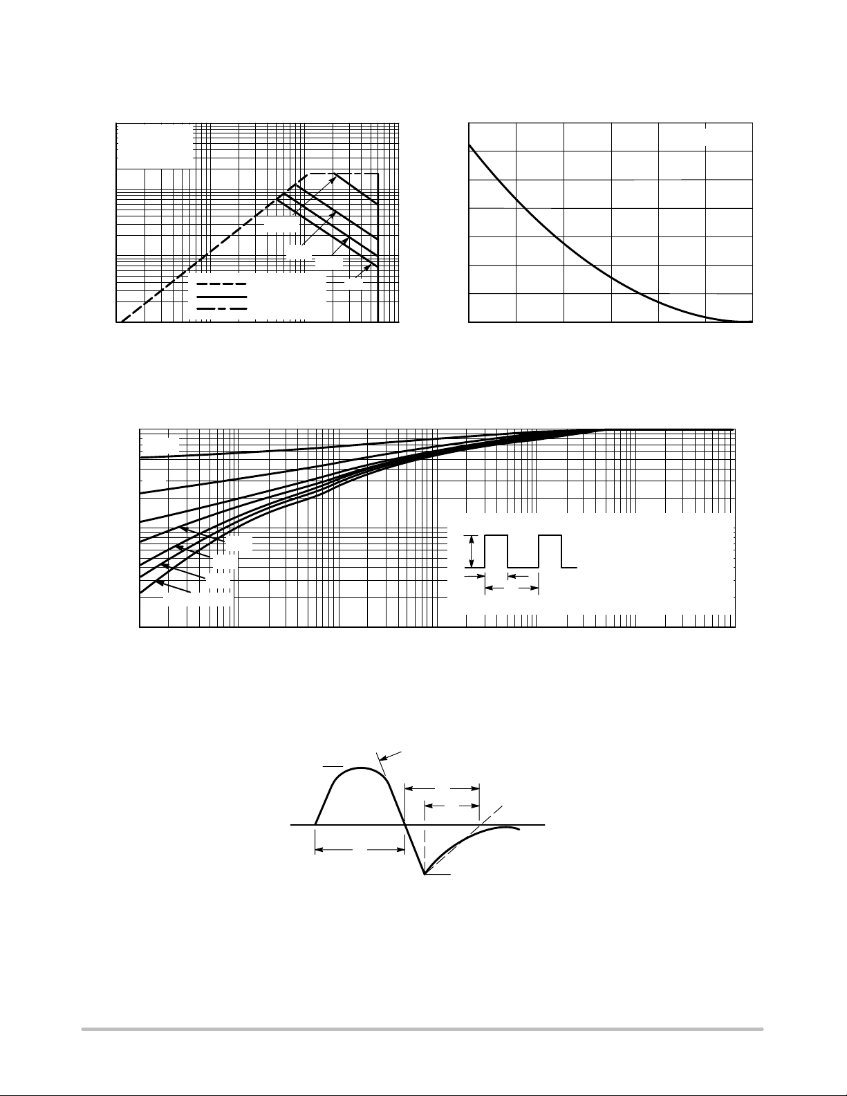
SAFE OPERATING AREA
The Forward Biased Safe Operating Area curves define the
maximum simultaneous drain−to−source voltage and drain
current that a transistor can handle safely when it is forward
biased. Curves are based upon maximum peak junction
temperature and a case temperature (TC) of 25°C. Peak
repetitive pulsed power limits are determined by using the
thermal response data in conjunction with the procedures
discussed in AN569, “Transient Thermal Resistance−General
Data and Its Use.”
Switching between the off−state and the on−state may
traverse any load line provided neither rated peak current
(IDM) nor rated voltage (V
) is exceeded and the
DSS
transition time (tr,tf) do not exceed 10 ms. In addition the total
power averaged over a complete switching cycle must not
exceed (T
J(MAX)
− TC)/(R
qJC
).
A Power MOSFET designated E−FET can be safely used
in switching circuits with unclamped inductive loads. For
http://onsemi.com
reliable operation, the stored energy from circuit inductance
dissipated in the transistor while in avalanche must be less
than the rated limit and adjusted for operating conditions
differing from those specified. Although industry practice is
to rate in terms of energy, avalanche energy capability is not
a constant. The energy rating decreases non−linearly with an
increase of peak current in avalanche and peak junction
temperature.
Although many E−FETs can withstand the stress of
drain−to−source avalanche at currents up to rated pulsed
current (IDM), the energy rating is specified at rated
continuous current (ID), in accordance with industry
custom. The energy rating must be derated for temperature
as shown in the accompanying graph (Figure 12). Maximum
energy at currents below rated continuous I
can safely be
D
assumed to equal the values indicated.
5
Page 6
MTD5P06V
SAFE OPERATING AREA
100
10
VGS = 20 V
SINGLE PULSE
TC = 25°C
140
120
100
80
100 ms
60
1
, DRAIN CURRENT (AMPS)
D
I
0.1
0.1
1
VDS, DRAIN−TO−SOURCE VOLTAGE (VOLTS)
Figure 11. Maximum Rated Forward Biased
Safe Operating Area
1 ms
R
LIMIT
DS(on)
THERMAL LIMIT
PACKAGE LIMIT
10
10 ms
40
dc
100
AVALANCHE ENERGY (mJ)
, SINGLE PULSE DRAIN−TO−SOURCE
20
AS
E
0
25 50 75 100 125
TJ, STARTING JUNCTION TEMPERATURE (°C)
Figure 12. Maximum Avalanche Energy versus
Starting Junction Temperature
1.0
D = 0.5
0.2
0.1
P
0.1
r(t), NORMALIZED EFFECTIVE
TRANSIENT THERMAL RESISTANCE
SINGLE PULSE
0.05
0.02
0.01
(pk)
t
1
t
2
DUTY CYCLE, D = t1/t
R
(t) = r(t) R
q
JC
q
JC
D CURVES APPLY FOR POWER
PULSE TRAIN SHOWN
READ TIME AT t
T
2
J(pk)
− TC = P
1
(pk)
R
0.01
1.0E−05 1.0E−04 1.0E−03 1.0E−02 1.0E−01 1.0E+00 1.0E+01
t, TIME (s)
Figure 13. Thermal Response
ID = 5 A
150
(t)
q
JC
175
di/dt
I
S
t
rr
t
t
a
b
TIME
t
p
0.25 I
S
I
S
Figure 14. Diode Reverse Recovery Waveform
http://onsemi.com
6
Page 7
MTD5P06V
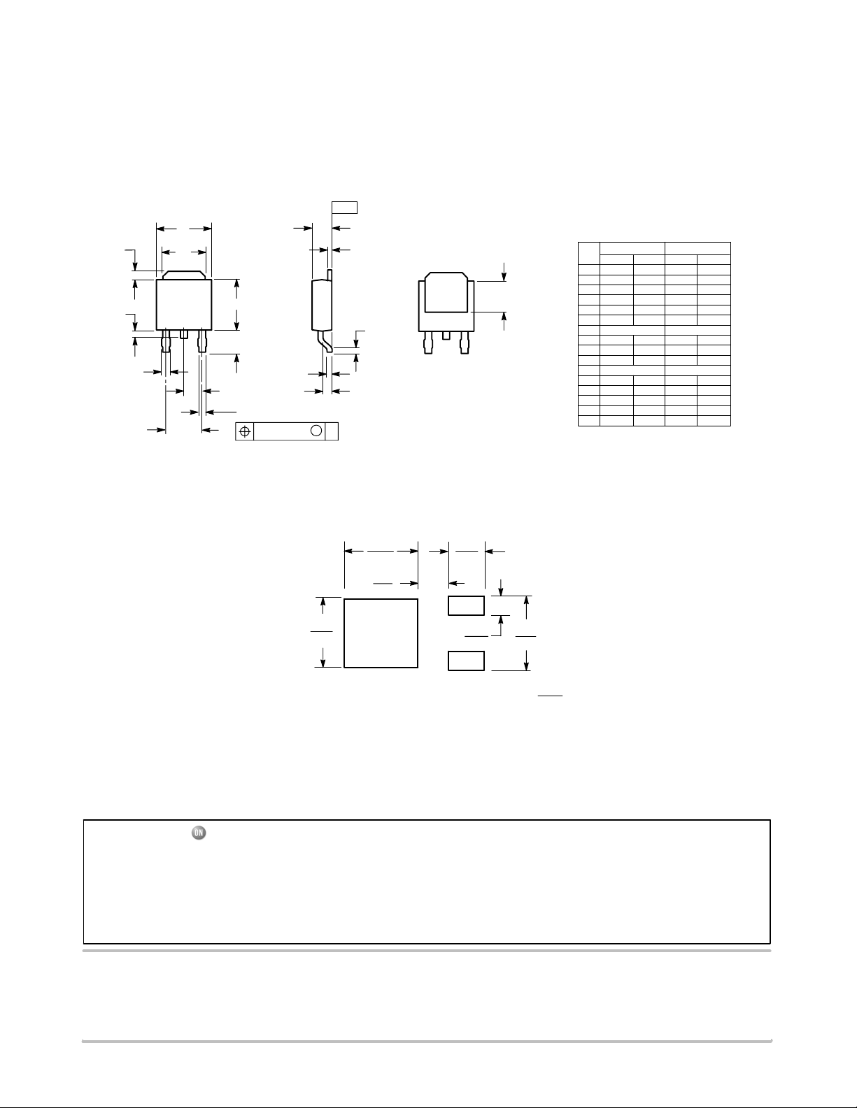
PACKAGE DIMENSIONS
DPAK
CASE 369C−01
ISSUE O
SEATING
−T−
PLANE
B
V
S
R
4
A
123
K
F
L
D
2 PL
G
0.13 (0.005) T
C
E
Z
U
J
H
M
NOTES:
1. DIMENSIONING AND TOLERANCING
PER ANSI Y14.5M, 1982.
2. CONTROLLING DIMENSION: INCH.
DIM MIN MAX MIN MAX
A 0.235 0.245 5.97 6.22
B 0.250 0.265 6.35 6.73
C 0.086 0.094 2.19 2.38
D 0.027 0.035 0.69 0.88
E 0.018 0.023 0.46 0.58
F 0.037 0.045 0.94 1.14
G 0.180 BSC 4.58 BSC
H 0.034 0.040 0.87 1.01
J 0.018 0.023 0.46 0.58
K 0.102 0.114 2.60 2.89
L 0.090 BSC 2.29 BSC
R 0.180 0.215 4.57 5.45
S 0.025 0.040 0.63 1.01
U 0.020 −−− 0.51 −−−
V 0.035 0.050 0.89 1.27
Z 0.155 −−− 3.93 −−−
STYLE 2:
PIN 1. GATE
2. DRAIN
3. SOURCE
4. DRAIN
MILLIMETERSINCHES
SOLDERING FOOTPRINT*
6.20
0.244
2.58
0.101
3.0
0.118
5.80
0.228
1.6
0.063
SCALE 3:1
6.172
0.243
ǒ
inches
mm
Ǔ
*For additional information on our Pb−Free strategy and soldering
details, please download the ON Semiconductor Soldering and
Mounting Techniques Reference Manual, SOLDERRM/D.
ON Semiconductor and are registered trademarks of Semiconductor Components Industries, LLC (SCILLC). SCILLC reserves the right to make changes without further notice
to any products herein. SCILLC makes no warranty, representation or guarantee regarding the suitability of its products for any particular purpose, nor does SCILLC assume any liability
arising out of the application or use of any product or circuit, and specifically disclaims any and all liability, including without limitation special, consequential or incidental damages.
“Typical” parameters which may be provided in SCILLC data sheets and/or specifications can and do vary in different applications and actual performance may vary over time. All
operating parameters, including “Typicals” must be validated for each customer application by customer’s technical experts. SCILLC does not convey any license under its patent rights
nor the rights of others. SCILLC products are not designed, intended, or authorized for use as components in systems intended for surgical implant into the body, or other applications
intended to support or sustain life, or for any other application in which the failure of the SCILLC product could create a situation where personal injury or death may occur. Should
Buyer purchase or use SCILLC products for any such unintended or unauthorized application, Buyer shall indemnify and hold SCILLC and its officers, employees, subsidiaries, affiliates,
and distributors harmless against all claims, costs, damages, and expenses, and reasonable attorney fees arising out of, directly or indirectly, any claim of personal injury or death
associated with such unintended or unauthorized use, even if such claim alleges that SCILLC was negligent regarding the design or manufacture of the part. SCILLC is an Equal
Opportunity/Affirmative Action Employer. This literature is subject to all applicable copyright laws and is not for resale in any manner.
PUBLICATION ORDERING INFORMATION
LITERATURE FULFILLMENT:
Literature Distribution Center for ON Semiconductor
P.O. Box 5163, Denver, Colorado 80217 USA
Phone: 303−675−2175 or 800−344−3860 Toll Free USA/Canada
Fax: 303−675−2176 or 800−344−3867 Toll Free USA/Canada
Email: [email protected]
N. American Technical Support: 800−282−9855 Toll Free
USA/Canada
Europe, Middle East and Africa Technical Support:
Phone: 421 33 790 2910
Japan Customer Focus Center
Phone: 81−3−5773−3850
http://onsemi.com
ON Semiconductor Website: www.onsemi.com
Order Literature: http://www.onsemi.com/orderlit
For additional information, please contact your local
Sales Representative
MTD5P06V/D
7
 Loading...