

Page 1
SEMICONDUCTOR TECHNICAL DATA
$ #
Order this document
by MTB8N50E/D
" "!
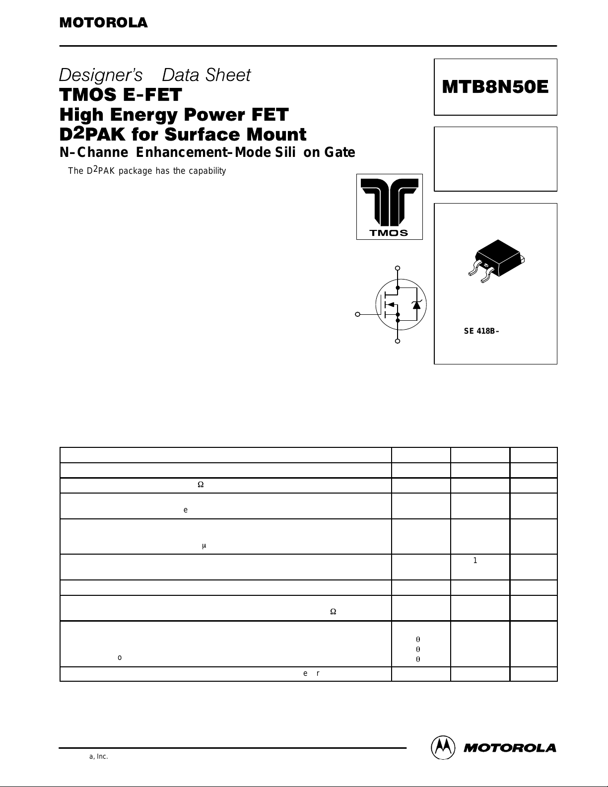
N–Channel Enhancement–Mode Silicon Gate
The D2PAK package has the capability of housing a larger die
than any existing surface mount package which allows it to be used
in applications that require the use of surface mount components
with higher power and lower R
MOSFET uses an advanced termination scheme to provide
enhanced voltage–blocking capability without degrading performance over time. In addition, this advanced TMOS E–FET is
designed to withstand high energy in the avalanche and commutation modes. This new energy efficient design also offers a
drain–to–source diode with a fast recovery time. Designed for low
voltage, high speed switching applications in power supplies,
converters, PWM motor controls, these devices are particularly well
suited for bridge circuits where diode speed and commutating safe
operating areas are critical and offer additional safety margin
against unexpected voltage transients.
• Robust High Voltage Termination
• Avalanche Energy Specified
• Source–to–Drain Diode Recovery Time Comparable
to a Discrete Fast Recovery Diode
• Diode is Characterized for Use in Bridge Circuits
• I
DSS
and V
Specified at Elevated Temperature
DS(on)
• Short Heatsink Tab Manufactured – Not Sheared
• Specifically Designed Leadframe for Maximum Power Dissipation
• Available in 24 mm 13–inch/800 Unit Tape & Reel, Add T4 Suffix to Part Number
MAXIMUM RATINGS
Drain–to–Source Voltage V
Drain–to–Gate Voltage (RGS = 1.0 MW)
Gate–to–Source Voltage – Continuous
Gate–to–Source Voltage – Non–repetitive (tp ≤ 10 ms)
Drain Current — Continuous @ TC = 25°C
Drain Current — Continuous @ TC = 100°C
Drain Current — Single Pulse (tp ≤ 10 ms)
Total Power Dissipation @ TC = 25°C
Derate above 25°C
Operating and Storage Temperature Range TJ, T
Single Pulse Drain–to–Source Avalanche Energy – STAR TING TJ = 25°C
(VDD = 25 Vdc, VGS = 10 Vdc, PEAK IL = 8.0 Apk, L = 16 mH, RG = 25 W)
Thermal Resistance
– Junction–to–Case
– Junction–to–Ambient
– Junction–to–Ambient
Maximum Lead Temperature for Soldering Purposes, 1/8″ from Case for 5 sec. T
(1) When surface mounted to an FR4 board using the minimum recommended pad size.
This document contains information on a new product. Specifications and information herein are subject to change without notice.
E–FET and Designer’s are trademarks of Motorola, Inc. TMOS is a registered trademark of Motorola, Inc.
REV 1
(TJ = 25°C unless otherwise noted)
(1)
capabilities. This high voltage
DS(on)
Rating
D
G
S
Symbol Value Unit
DSS
V
DGR
V
GS
V
GSM
I
D
I
D
I
DM
P
D
stg
E
AS
R
q
JC
R
q
JA
R
q
JA
L
TMOS POWER FET
8.0 AMPERES
500 VOL TS
R
CASE 418B–02, Style 2
–55 to 150 °C
= 0.8 OHM
DS(on)
D2PAK
500 Vdc
500 Vdc
±20
±40
8.0
5.0
32
125
1.0
510 mJ
1.0
62.5
50
260 °C
Vdc
Vpk
Adc
Apk
Watts
W/°C
°C/W
Motorola TMOS Power MOSFET Transistor Device Data
Motorola, Inc. 1996
1
Page 2
MTB8N50E
)
f = 1.0 MHz)
(R
W
)
(
DS
,
D
,
(
S
,
GS
,
ELECTRICAL CHARACTERISTICS
OFF CHARACTERISTICS
Drain–to–Source Breakdown Voltage
(VGS = 0 Vdc, ID = 250 µAdc)
T emperature Coef ficient (Positive)
Zero Gate Voltage Drain Current
(VDS = 500 Vdc, VGS = 0 Vdc)
(VDS = 400 Vdc, VGS = 0 Vdc, TJ = 125°C)
Gate–Body Leakage Current
(VGS = ±20 Vdc, VDS = 0 Vdc)
ON CHARACTERISTICS
Gate Threshold Voltage
(VDS = VGS, ID = 250 µAdc)
Threshold Temperature Coefficient (Negative)
Static Drain–to–Source On–Resistance
(VGS = 10 Vdc, ID = 4.0 Adc)
Drain–to–Source On–Voltage (VGS = 10 Vdc)
(ID = 8.0 Adc)
(ID = 4.0 Adc, TJ = 125°C)
Forward Transconductance
(VDS = 15 Vdc, ID = 4.0 Adc)
DYNAMIC CHARACTERISTICS
Input Capacitance
Output Capacitance
Transfer Capacitance
SWITCHING CHARACTERISTICS
Turn–On Delay Time
Rise Time
Turn–Off Delay Time
Fall Time t
Gate Charge
(see Figure 8)
SOURCE–DRAIN DIODE CHARACTERISTICS
Forward On–Voltage
(IS = 8.0 Adc, VGS = 0 Vdc) — 1.2 2.0
(IS = 8.0 Adc, VGS = 0 Vdc, TJ = 125°C) — 1.1 —
Reverse Recovery Time
Reverse Recovery Stored Charge Q
INTERNAL PACKAGE INDUCTANCE
Internal Drain Inductance
(Measured from the drain lead 0.25″ from package to center of die)
Internal Source Inductance
(Measured from the source lead 0.25″ from package to source bond pad)
(1) Pulse Test: Pulse Width ≤ 300 ms, Duty Cycle ≤ 2.0%.
(2) Switching characteristics are independent of operating junction temperature.
(1)
(T
C
Characteristic
(VDS = 25 Vdc, VGS = 0 Vdc,
(2)
(VDS = 400 Vdc, ID = 8.0 Adc,
(IS = 8.0 Adc, VGS = 0 Vdc,
= 25°C unless otherwise noted)
f = 1.0 MHz
= 9.1
Gon
VGS = 10 Vdc)
dIS/dt = 100 A/ms)
Symbol Min Typ Max Unit
V
(BR)DSS
I
DSS
I
GSS
V
GS(th)
R
DS(on)
V
DS(on)
g
FS
C
iss
C
oss
C
rss
t
d(on)
t
r
t
d(off)
f
Q
T
Q
1
Q
2
Q
3
V
SD
t
rr
t
a
t
b
RR
L
D
L
S
500
—
—
—
— — 100
2.0
—
— 0.6 0.8
—
—
4.0 — —
— 1450 1680 pF
— 190 264
— 45.4 144
— 15 50 ns
— 33 72
— 40 150
— 32 60
— 40 64 nC
— 8.0 —
— 17 —
— 17.3 —
— 320 — ns
— 179 —
— 141 —
— 3.0 —
— 4.5 —
— 7.5 —
—
500
—
—
3.0
6.3
—
—
—
—
10
100
4.0
—
7.2
6.4
Vdc
mV/°C
m
Adc
nAdc
Vdc
mV/°C
Ohms
Vdc
mhos
Vdc
m
C
nH
2
Motorola TMOS Power MOSFET Transistor Device Data
Page 3

TYPICAL ELECTRICAL CHARACTERISTICS
MTB8N50E
16
12
8.0
, DRAIN CURRENT (AMPS)
4.0
D
I
0
TJ = 25°C
VDS, DRAIN–TO–SOURCE VOL TAGE (VOLTS)
VGS = 10 V
8 V
108.06.04.02.00
Figure 1. On–Region Characteristics
1.6
1.4
VGS = 10 V
1.2
1.0
0.8
0.6
0.4
0.2
, DRAIN–TO–SOURCE RESIST ANCE (OHMS)
0
DS(on)
R
4.0 8.0 12 16 2.0 6.0 10 14
ID, DRAIN CURRENT (AMPS)
TJ = 100°C
Figure 3. On–Resistance versus Drain Current
and T emperature
25°C
–55°C
16
7 V
6 V
5 V
, DRAIN CURRENT (AMPS)
D
I
1412
VDS ≥ 10 V
14
12
10
8.0
6.0
4.0
2.0
0
2.0 2.5 4.0 4.5 5.0 5.5 6.0 6.5 7.0
3.0 3.5
VGS, GATE–T O–SOURCE VOLTAGE (VOLTS)
100°C
25°C
TJ = –55°C
Figure 2. Transfer Characteristics
0.90
TJ = 25°C
0.85
0.80
0.75
0.70
0.65
0.60
, DRAIN–TO–SOURCE RESIST ANCE (OHMS)
0.55
14106.02.00
DS(on)
0 4.0 8.0 12 16
R
ID, DRAIN CURRENT (AMPS)
VGS = 10 V
15 V
Figure 4. On–Resistance versus Drain Current
and Gate Voltage
2.5
VGS = 10 V
ID = 8 A
2.0
1.5
1.0
0.5
, DRAIN–TO–SOURCE RESIST ANCE (NORMALIZED)
0
DS(on)
R
TJ, JUNCTION TEMPERATURE (°C)
1257525–25
Figure 5. On–Resistance Variation with
T emperature
Motorola TMOS Power MOSFET Transistor Device Data
100,000
VGS = 0 V
10,000
1,000
, LEAKAGE (nA)
100
DSS
I
10
1.0
150100500–50
0 100 300 500200 400
VDS, DRAIN–TO–SOURCE VOL TAGE (VOLTS)
TJ = 125°C
100°C
25°C
Figure 6. Drain–to–Source Leakage Current
versus V oltage
3
Page 4

MTB8N50E
TYPICAL ELECTRICAL CHARACTERISTICS
4000
VDS = 0 V VGS = 0 V
3000
2000
C, CAPACITANCE (pF)
1000
C
iss
C
rss
C
oss
C
0
VGSV
GATE–T O–SOURCE OR DRAIN–TO–SOURCE VOLTAGE (VOLTS)
rss
15 25
DS
Figure 7. Capacitance Variation
12
QT
10
, GATE–T O–SOURCE VOLT AGE (VOLTS)
GS
V
8.0
6.0
4.0
2.0
Q2Q1
Q3
0
Qg, TOTAL GATE CHARGE (nC)
V
GS
V
DS
Figure 9. Gate–to–Source and
Drain–to–Source V oltage versus Total Charge
TJ = 25°C
C
iss
20105.00–5.0–10
TJ = 25°C
ID = 8 A
3224168.00
40
400
300
200
100
0
DS
V
, DRAIN–TO–SOURCE VOL TAGE (VOLTS)
10,000
VGS = 0 V TJ = 25°C
C
iss
1,000
C
C
oss
rss
100
C, CAPACITANCE (pF)
10
10 100 1000
DRAIN–TO–SOURCE VOLTAGE (VOLTS)
Figure 8. High V oltage Capacitance Variation
1000
TJ = 25°C
ID = 8 A
VDD = 250 V
VGS = 10 V
100
t, TIME (ns)
t
d(off)
t
r
t
f
t
10
1.0 10 100
d(on)
RG, GATE RESISTANCE (OHMS)
Figure 10. Resistive Switching Time V ariation
versus Gate Resistance
8.0
6.0
4.0
2.0
, SOURCE CURRENT (AMPS)
S
I
0
4
TJ = 25°C
VGS = 0 V
0.90.80.70.60.5
VSD, SOURCE–TO–DRAIN VOL TAGE (VOLTS)
Figure 11. Diode Forward Voltage versus
Current
100
VGS = 20 V
SINGLE PULSE
TC = 25
°
10
1.0
0.1
, DRAIN CURRENT (AMPS)
D
I
1.31.21.11.0
0.01
0.1 1.0 10 100 1000
C
R
LIMIT
DS(on)
THERMAL LIMIT
PACKAGE LIMIT
VDS, DRAIN–TO–SOURCE VOL TAGE (VOLTS)
10 ms
100 ms
1 ms
10 ms
dc
Figure 12. Maximum Rated Forward Biased
Safe Operating Area
Motorola TMOS Power MOSFET Transistor Device Data
Page 5

1.0
D = 0.5
0.2
600
500
400
300
200
AVALANCHE ENERGY (mJ)
100
, SINGLE PULSE DRAIN–TO–SOURCE
AS
E
0
Figure 13. Maximum Avalanche Energy versus
ID = 8 A
50 100
TJ, STARTING JUNCTION TEMPERATURE (°C)
75 125
Starting Junction T emperature
MTB8N50E
15025
0.1
0.1
0.05
0.02
r(t), NORMALIZED EFFECTIVE
TRANSIENT THERMAL RESISTANCE
0.01
0.01
SINGLE PULSE
0.00001
0.0001 0.001 0.01 1.0 10
t, TIME (seconds)
0.1
Figure 14. Thermal Response
Motorola TMOS Power MOSFET Transistor Device Data
5
Page 6

MTB8N50E
–T–
SEATING
PLANE
PACKAGE DIMENSIONS
C
E
B
V
A
S
K
G
D
3 PL
0.13 (0.005) T
M
J
H
NOTES:
1. DIMENSIONING AND TOLERANCING PER ANSI
Y14.5M, 1982.
2. CONTROLLING DIMENSION: INCH.
PIN 1. GATE
2. DRAIN
3. SOURCE
4. DRAIN
MILLIMETERSINCHES
DIM MIN MAX MIN MAX
A 0.340 0.380 8.64 9.65
B 0.380 0.405 9.65 10.29
C 0.160 0.190 4.06 4.83
D 0.020 0.035 0.51 0.89
E 0.045 0.055 1.14 1.40
G 0.100 BSC 2.54 BSC
H 0.080 0.110 2.03 2.79
J 0.018 0.025 0.46 0.64
K 0.090 0.110 2.29 2.79
S 0.575 0.625 14.60 15.88
V 0.045 0.055 1.14 1.40
STYLE 2:
CASE 418B–02
ISSUE B
Motorola reserves the right to make changes without further notice to any products herein. Motorola makes no warranty , representation or guarantee regarding
the suitability of its products for any particular purpose, nor does Motorola assume any liability arising out of the application or use of any product or circuit, and
specifically disclaims any and all liability, including without limitation consequential or incidental damages. “T ypical” parameters which may be provided in Motorola
data sheets and/or specifications can and do vary in different applications and actual performance may vary over time. All operating parameters, including “Typicals”
must be validated for each customer application by customer’s technical experts. Motorola does not convey any license under its patent rights nor the rights of
others. Motorola products are not designed, intended, or authorized for use as components in systems intended for surgical implant into the body, or other
applications intended to support or sustain life, or for any other application in which the failure of the Motorola product could create a situation where personal injury
or death may occur. Should Buyer purchase or use Motorola products for any such unintended or unauthorized application, Buyer shall indemnify and hold Motorola
and its officers, employees, subsidiaries, affiliates, and distributors harmless against all claims, costs, damages, and expenses, and reasonable attorney fees
arising out of, directly or indirectly, any claim of personal injury or death associated with such unintended or unauthorized use, even if such claim alleges that
Motorola was negligent regarding the design or manufacture of the part. Motorola and are registered trademarks of Motorola, Inc. Motorola, Inc. is an Equal
Opportunity/Affirmative Action Employer.
How to reach us:
USA/EUROPE/ Locations Not Listed: Motorola Literature Distribution; JAPAN: Nippon Motorola Ltd.; Tatsumi–SPD–JLDC, 6F Seibu–Butsuryu–Center,
P.O. Box 5405, Denver, Colorado 80217. 303–675–2140 or 1–800–441–2447 3–14–2 Tatsumi Koto–Ku, Tokyo 135, Japan. 81–3–3521–8315
Mfax: RMFAX0@email.sps.mot.com – TOUCHTONE 602–244–6609 ASIA/PACIFIC: Motorola Semiconductors H.K. Ltd.; 8B Tai Ping Industrial Park,
INTERNET: http://Design–NET.com 51 Ting Kok Road, Tai Po, N.T., Hong Kong. 852–26629298
6
◊
Motorola TMOS Power MOSFET Transistor Device Data
MTB8N50E/D
 Loading...