

Page 1
2
ISO
-CMOS ST-BUS FAMILY
MT9174
Digital Network Interface Circuit
with Receive Sync Marker Bit
Features
• Receive sync output pulse
• Full duple x trans mis sion o ver a si ngle twist ed
pair
• Selectable 80 or 160 kbit/s line rate
• Adaptive echo can cellati on
• Up to 4 km loop reach
• ISDN compatible (2B+D) data format
• Transparent modem capability
• Frame synchronization and clock extraction
• MITEL ST-BUS compatible
• Low power (typically 50 mW), single 5V supply
Applications
•TDD Digital PCS (DECT, CT2, PHS) base
stations re quiring c ell sy nchr onizati on
• Digital subscriber lines
• High speed data trans mis sion ov er twi sted
wires
• Digital PABX line car ds and t eleph one s ets
• 80 or 160 k bit/s si ngle chip mode m
ISSUE 1 May 1995
Ordering Info rm ation
MT9174AE 24 Pin Plastic DIP
MT9174A N 24 Pin SS OP
MT9174AP 28 Pin PLCC
-40°C to
+85°C
Description
The MT9174 is identical to the MT9172 in all
respects except for the addition of one feature. The
MT9174 includes a digital output pin indicating the
temporal position of the "SYNC" bit of the biphase
transmission. This feature is especially useful for
systems such as PCS wireless base stations
applications requiring close synchronization between
microcells.
The MT9174 is fabricated in Mitel’s ISO
process.
2
-CMOS
DSTi/Di
CDSTi/
CDi
/CLD
F0
C4/TCK
F0o/RCK
MS0
MS1
MS2
RegC
DSTo/Do
CDSTo/
CDo
RxSB
Transmit
Interface
Control
Register
Transmit/
Clock
Receive
Timing &
Control
Status
Receive
Interface
Prescrambler Scrambler
Transmit
Timing
Master Clock
Phase Locked
Sync Detect
Receive
Differentially
Encoded Biphase
Transmitter
Address
Echo Cance ller
Error
DPLL
De-
Prescrambler
Signa l
Descrambler
V
DDVSSVBiasVRef
Echo Estimate
—
+
∑
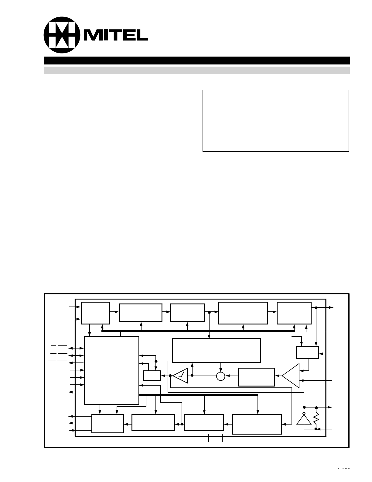
Figure 1 - Functional Block Diagram
Receive
Filter
Differentially
Encoded Biphase
Receiver
Transmit
Filter &
Line Driver
V
Bias
-1
+2
MUX
L
OUT
L
OUT
DIS
Precan
L
IN
OSC2
OSC1
9-1559-155
Page 2
MT9174 Advance Information
LOUT
VBias
VRef
NC
VDD
LIN
TEST
LOUT
VBias
VRef
MS2
MS1
MS0
RegC
RxSB
/CLD
F0
CDSTi/CDi
CDSTo/CDo
VSS
Pin Description
1
2
3
4
5
6
7
8
9
10
11
12
24 PIN PDIP/ SSOP
24
23
22
21
20
19
18
17
16
15
14
13
VDD
LIN
TEST
LOUT DIS
Precan
OSC1
NC
OSC2
/TCK
C4
F0o/RCK
DSTi/Di
DSTo/Do
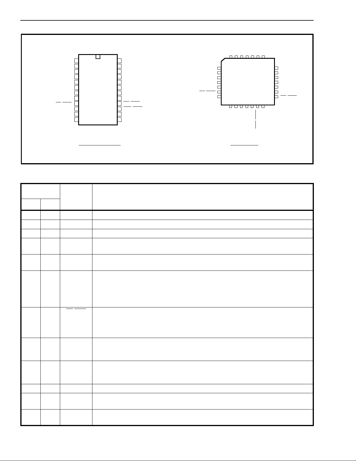
Figure 2 - Pin Connections
F0
MS2
NC
MS1
MS0
RegC
/CLD
RxSB
432
5
6
7
8
9
10
11
1213141516
CDSTi/CDi
CDSTo/CDo
28 PIN PLCC
•
VSS
1
27
28
26
NC
25
LOUT DIS
24
23
Precan
22
OSC1
21
OSC2
20
NC
19
17
18
NC
/RCK
DSTi/Di
F0o
DSTo/Do
C4
/TCK
Pin #
Name Descrip tio n
24 28
12 L
23 V
34 V
OUT
Bias
Ref
Line Out. Transmit Signal out put (Anal og). Referenced to V
Bias
.
Internal Bias Voltage output . Connect via 0.33 µF decoupling capacitor to VDD.
Internal Reference Voltage output. Connect via 0.33 µF decoupling capacitor to VDD.
4,5,65,7,8MS2-MS0 Mode Select inputs (Digital). The logic levels present on these pins select the various
operating modes for a particular applicat ion. See Table 1 for the operating modes.
79RegCRegulator Control outpu t (Digital). A 512 kHz clock used for switch mode power
supplies. Unused in MAS/MOD mode and should be left open circuit.
8 11 RxSB Receive Sync Bit output (Digit al). Th is output is held high unt il receive
synchronizat ion occurs (i.e., until the sync bit in Status Register =1). Once low,
indicating synchronized transmission, a high going pulse (6.24 µs wide pulse @ 160
kb/s and 12.5 µs wide @ 80 kb/s) indicates the tem poral positio n of the receive
"SYNC" bit in the biphase line transmission.
910F0
/CLD Frame Pulse/C-Channel Load (Digital ). In DN mode a 244 ns wide negative pulse
input for the MASTER indicat ing t he start of the acti ve channel tim es of the device.
Output for the SLAVE indicating the start of the active channel times of the device.
Output in MOD mode providi ng a pulse indicat ing the start of the C-cha nnel.
10 12 CDSTi/
CDi
Control/Data ST-BUS In/Control/Data In (Digital). A 2.048 Mbit/s serial control &
signalling input in DN mode. In MOD mode this is a continuous bit stream at the bit
rate selected.
11 13 CDSTo/
CDo
Control/Data ST-BUS Out/Control/Data Out (Digital). A 2.048 Mbit/s serial control &
signalling output in DN mode. In MOD mode this is a continuous bit stream at the bit
rate selected.
12 14 V
SS
Negative Pow er Su pp ly (0V) .
13 15 DSTo/Do Data ST-BUS Out/Data Out (Digital). A 2.048 Mbit/s serial PCM/data output in DN
mode. In MOD mode this is a continuous bit stream at the bit rate selected.
14 16 DSTi/Di Data ST-BUS In/Data In (Digital). A 2.048 Mbit/ s serial P C M /data input in DN mode.
In MOD mode this is a continuous bit stream at the bit rate selected.
9-156
Page 3
Advance Information MT9174
Pin Description (continued)
Pin #
Name Descrip tio n
24 28
15 17 F0o/RCK Frame Pulse Out/Receive Bit Rate Clock output (Digital). In DN mode a 244 ns
wide negative pulse indicat ing the end of the active channel times of the device to
allow daisy chaining. In MOD mode provides the receive bit rate clock to the system.
16 19 C4
/TCK Data Clock/Transmit Baud Rate Clock (Digital). A 4.096 MHz TTL compatible clock
input for the MASTER and output for the SLA VE in DN mode. For MOD mode this pin
provides the transmit bit rate clock to the system.
17 21 OSC2 Oscillator Output. CMOS Output.
19 22 OSC1 Oscillator Input. CMOS Input. D.C. couple signals to this pin. Refer to D.C. Electrical
Characteristics for OSC1 input requirement s.
20 23 Precan Precanceller Disable. When held to Logic ’1’
precanceller is forced to V
the L
to the precanceller path is enabled and functions normally. An internal
OUT
thus bypassing the precanceller section. When logic ’0’,
Bias
, the internal path from L
OUT
to the
pulldown (50 kΩ) is provided on this pin.
18 1,6,
NC No Connection. Leave open circuit
18,
20,
25
21 24 L
OUT
DIS L
22 26 TEST Test Pin. Connect to V
23 27 L
24 28 V
IN
DD
Disable. When held t o logic “1”, L
OUT
logic “0”, L
functions normally. An internal pulldown (50 kΩ) is provided on this pin.
OUT
.
SS
Receive Signal input (Analog).
Positive Power Supply (+5V) input.
is disabled (i.e., output = V
OUT
). When
Bias
9-157
Page 4

MT9174 Advance Information
NOTES:
9-158
 Loading...