

Page 1
AAAA
AAAA
AAAA
AAAA
AAAA
A
A
A
A
A
A
A
A
A
A
AA
ISO
2
-CMOS
MT9160
5 Volt Multi-Featured Codec (MFC)
Preliminary Information
Features
• Programmable µ-Law/A-Law C ode c and Fi lters
• Program mable CCITT (G .711)/sign-magni tude
coding
• Program mab le trans mit , receiv e and si de-t one
gains
• Fully di fferential in terfac e to han dse t
transduce rs - inc luding 3 00 o hm rece iver dri ver
• Flexibl e digit al inter face i ncluding ST-BUS/SSI
• Serial mi croport or def ault co ntrol lerle ss mode
• Singl e 5 volt s upply
• Low pow er opera tio n
• CCITT G.714 com p li an t
Applications
• Digita l telep hone s ets
• Cel lu lar rad io set s
• Local area com m unications stations
•Pair Gain Systems
• Line ca rds
ISSUE 3 May 1995
Ordering Information
MT9160AE 24 Pin Plastic D IP
MT9160AS 20 Pin SOIC
-40°C to +85°C
Descript io n
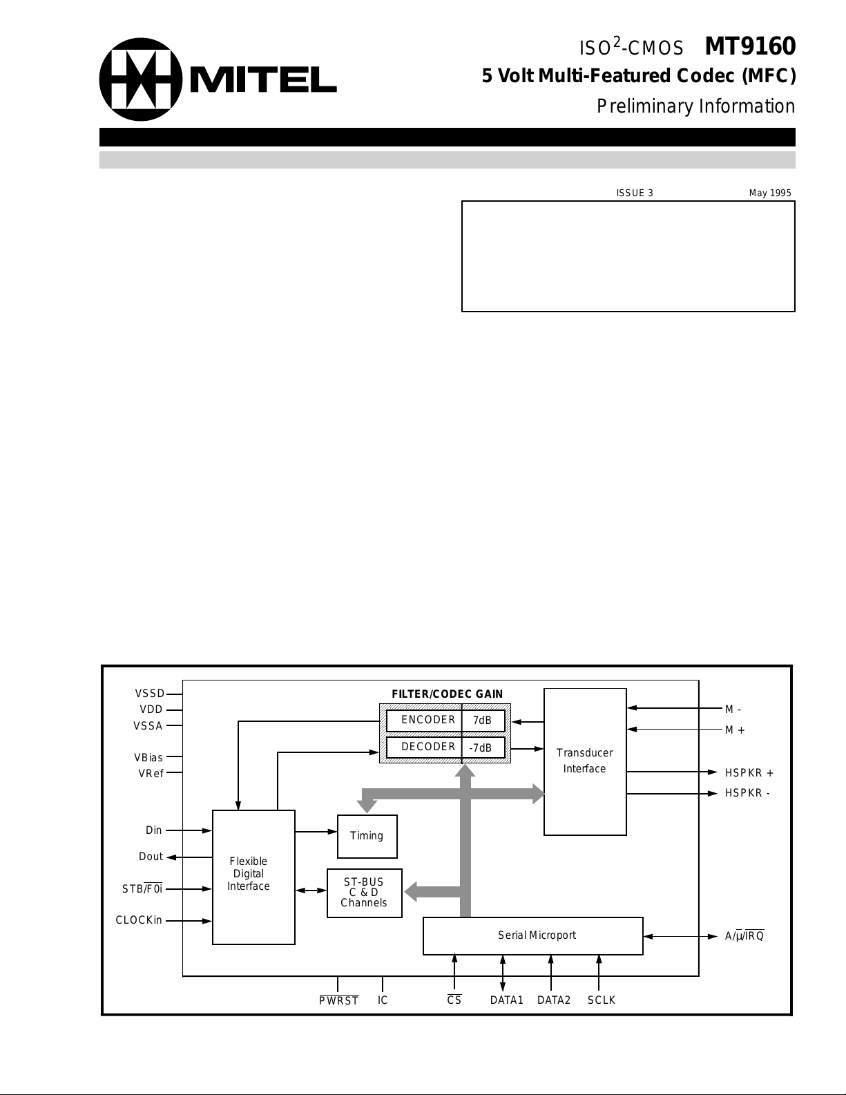
The MT9160 5V Multi-featured Codec incorporates a
built-in Filter/Codec, gain control and programmable
sidetone path as well as on-chip anti-alias filters,
reference voltage and bias source. The device
supports both A-Law and µ-Law requirements.
Complete telephony interfaces are provided for
connection to handset transducers. Internal register
access is provided through a serial microport
compatible with various industry standard
micro-controllers. The device also supports
controllerless operation utilizing the default register
conditions.
The MT9160 is fabricated in Mitel's ISO
technology ensuring low power consumption and
high reliability.
2
-CMOS
STB/F0i
CLOCKin
VSSD
VDD
VSSA
VBias
VRef
Dout
Din
Flexible
Digital
Interface
FILTER/CODEC GAIN
AAA
AAAA
AAAA
AAAA
AAAA
AAAA
AAA
AAAA
AAA
AAAA
ENCODER
AAA
AAAA
AAA
AAAA
AAA
AAAA
AAA
AAAA
AAA
AAAA
DECODER
AAA
AAAA
AAA
AAAA
AAA
AAAA
AAAA
AAAA
AAAA
AAAA
AAAA
AAAA
AAAA
AAAA
AAAA
AAAA
AAAA
AAAA
AAAA
AAAA
AAAA
AAAA
AAAA
AAAA
AAAA
AAAA
AAAA
AAAA
AAAA
AAAA
AAAA
AAAA
AAAA
AAAA
AAAA
AAAA
AAAA
AAAA
7dB
AAAA
AAAA
AAAA
AAAA
AAAA
-7dB
AAAA
AAAA
AAAA
A
A
A
A
A
A
A
A
A
A
A
Timing
ST-BUS
C & D
Channels
Serial Microport
PWRST
IC
CS DA T A1 DATA2 SCLK
Figure 1 - Functional Block Diagram
Transducer
Interface
M M +
HSPKR +
HSPKR -
A/µ/IRQ
7-77
Page 2
MT9160 Preliminary Information
20 PIN SOIC
24 PIN PDIP
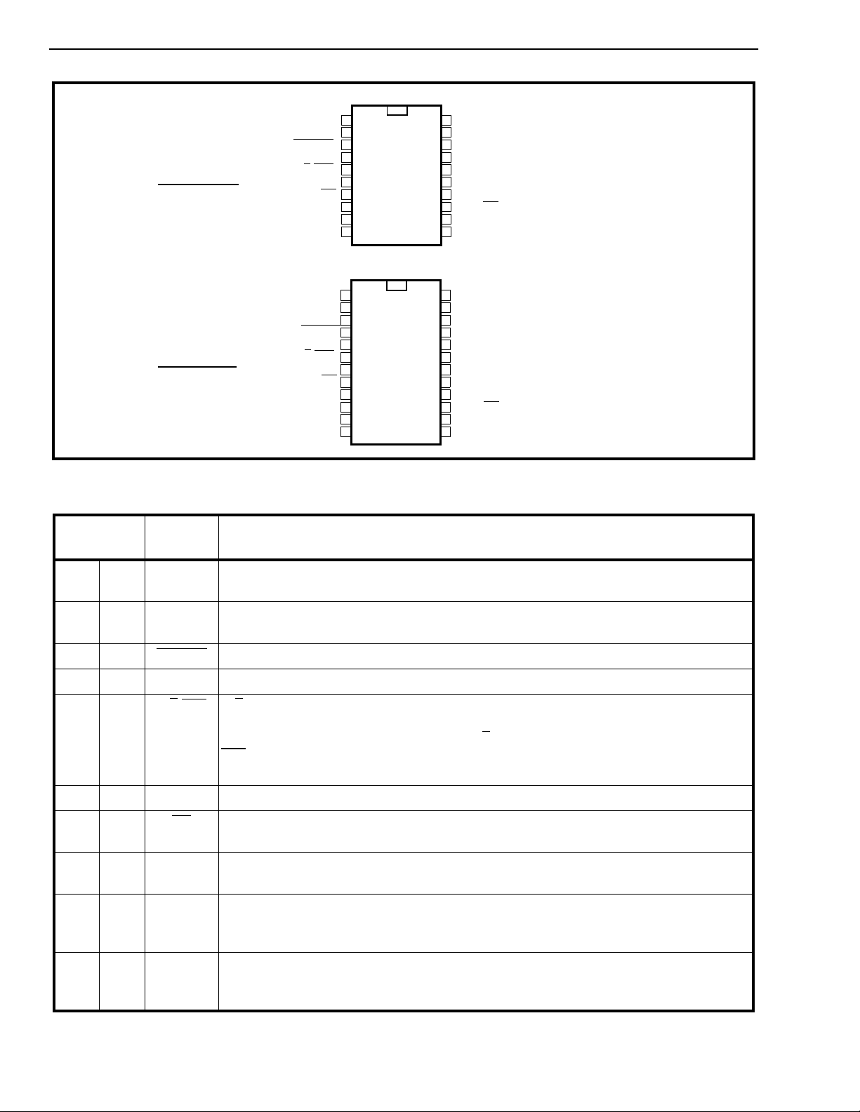
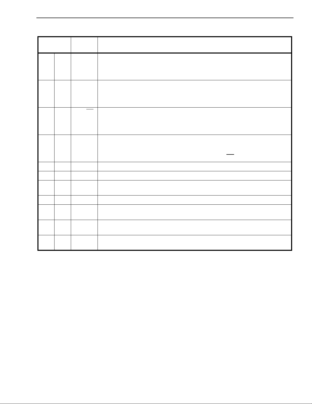
Pin Description
IC
CS
NC
IC
CS
NC
1
2
3
4
5
6
7
8
9
10 11
1
2
3
4
5
6
7
8
9
10
11
12
20
19
18
17
16
15
14
13
12
24
23
22
21
20
19
18
17
16
15
14
13
VBias
VRef
PWRST
A/µ/IRQ
VSSD
SCLK
DATA1
DATA2
VBias
VRef
PWRST
A/µ/IRQ
VSSD
SCLK
DATA1
DATA2
Figure 2 - Pin Connections
M +
M VSSA
HSPKR +
HSPKR VDD
CLOCKin
STB/F0i
Din
Dout
M +
M VSSA
NC
HSPKR +
HSPKR VDD
CLOCKin
NC
STB/F0i
Din
Dout
Pin #
SOIC DIP
11V
22 V
3 4 PWRST
45 ICInternal Conne ction. Tie externally to V
56A/µ
Name Description
Bias
Ref
Bias Voltage (Output). (VDD/2) volts is available at this pin for biasing external
amplifiers. Connect 0.1 µF capacitor to V
SSA
.
Reference Voltage for Codec (Output). Nominally [(VDD/2)-1.5] volts. Used
internally. Connect 0.1 µF capacitor to V
SSA
.
Power-up Reset (Input). CMOS comp atib le input with Schmitt Trigger (active low).
for normal operation.
SS
/IRQ A/µ - When internal control bit DEn = 0 this CMOS level compatible input pin governs
the companding law used by the filter/Code c; µ -Law when tie d to V
when tied to V
IRQ
- When internal control bit DEn = 1 this pin becomes an open-drain inter rupt
. Logically OR’ed with A/µ register bit .
DD
and A-Law
SS
output signalling valid access to the D-Channel registers in ST-BUS mode.
67V
SSD
78 CS
Digital Groun d. Nomi nally 0 volts.
Chip Select (Input). This input signal is used to select the device for microport data
transfers. Active low. TTL level compatible.
810SCLKSerial Port Synch ro nou s Clo ck (In put). Data clock for microport. TTL level
compatible.
911DATA 1Bidirectional Serial Data. Port for microprocessor serial data transfer. In Motorola/
National mode of operation, this pin becomes the dat a transmit pin only and data
receive is performed on the DATA 2 pin. Input TTL level compatible.
10 12 DATA 2 Serial Data Receive. In Motorola/Nat ional mode of operati on, this pin is used for
data receive. In Intel mode, serial data transmit and receive are performed on the
DATA 1 pin and DATA 2 is disconnected. Input TTL level compatible.
7-78
Page 3
Preliminary Information MT9160
Pin Description (continued)
Pin #
SOIC DIP
11 13 D
Name Description
out
Data Output. A high impedance three-state digital output for 8 bit wide channel data
being sent to the Layer 1 transceiver. Data is shifted out via this pin concurrent with
the rising edge of the bit clock during the timeslot defined by STB, or according to
standard ST-BUS timing.
12 14 D
Data Input. A digital input for 8 bit wide channel data received from the Layer 1
in
transceiver. Data is sampled on the falling edge of the bit clock during the timeslot
defined by STB, or according to standard ST-BUS timing. Input level is CMOS
compatibl e.
13 15 STB/F0i
Data Strobe/Frame Pulse (Input). For SSI mode this input determine s the 8 bit
timeslot used by the device for both transmit and receive data. This active high signal
has a repetition rate of 8 kHz. Standard frame pulse defini tions ap ply in ST-BUS
mode (refer to Figure 11). CMOS level compatible input.
14 17 CLOCKin Clock (Input). (CM OS level compatib le). Th e clock provided to this input pin is used
for the internal device functions. For SSI mode connect the bit clock to this pin when
it is 512 kHz or greater. Connect a 4096 kHz clock to this input when the available bit
15 18 V
DD
clock is 128 kHz or 256 kHz. For ST-BUS mode connect C4i
Positive Po wer Supply (Inp ut). Nominally 5 volt s .
to this pin.
16 19 HSPKR- Invertin g Hand set Speaker (Outpu t). Output to the handset speaker (balanced).
17 20 HSPKR+ N on-I nver tin g Hand set Speaker (Output). Output to the handse t speaker
(balanced).
18 22 V
SSA
Analog Gr ou nd (In pu t). Nominally 0 volts.
19 23 M- Invertin g Micro ph on e (Inp ut). Inverting input to microp hone am plif ier from the
handset microphone.
20 24 M+ Non-Inverting Micro ph one (Input). Non-invert ing input to microphone am plif ier
from the handset microphone.
3,9,
NC No Connect. (DIP Package only).
16,21
7-79
Page 4

MT9160 Preliminary Information
Overview
The 5V Multi-featured Codec (MFC) features
complete Analog/Digital and Digital/Analog
conversion of audio signals (Filter/Codec) and an
analog interface to a standard handset transmitter
and receiver (Transducer Interface). The receiver
amplifier is capable of driving a 300 ohm load.
Each of the programmable parameters within the
functional blocks is accessed through a serial
microcontroller port compatible with Intel MCS-51
Motorola SPI
Microwire
®
®
and National Semiconductor
specifications. These parameters
®
include: gain control, power down, mute, B-Channel
select (ST-BUS mode), C&D channel control/access,
law control, digital interface programming and
loopback. Optionally the device may be used in a
controllerless mode utilizing the power-on default
settings.
Functional Description
Filter/Codec
design. This fully differential architecture is
continued into the Transducer Interface section to
provide full chip realization of these capabilities for
the handset functions.
A reference voltage (V
), for the conversion
Ref
requirements of the Codec section, and a bias
voltage (V
), for biasing the internal analog
Bias
sections, are both generated on-chip. V
brought to an external pin so that it may be used for
biasing external gain setting amplifiers. A 0.1µF
capacitor must be connected from V
,
ground at all times. Likewise, although V
Bias
be used internally, a 0.1µF capacitor from the V
pin to ground is required at all times. The analog
ground reference point for these two capacitors must
be physically the same point. To facilitate this the
V
Ref
and V
pins are situated on adjacent pins.
Bias
The transmit filter is designed to meet CCITT G.714
specifications. The nominal gain for this filter is 0 dB
(gain control = 0 dB). Gain control allows the output
signal to be increased up to 7 dB. An anti-aliasing
filter is included. This is a second order lowpass
implementation with a corner frequency at 25 kHz.
is also
Bias
to analog
may only
Ref
Ref
The Filter/Codec block implements conversion of the
analog 0-3.3 kHz speech signals to/from the digital
domain compatible with 64 kb/s PCM B-Channels.
Selection of companding curves and digital code
assignment are programmable. These are CCITT
G.711 A-law or µ-Law, with true-sign/ Alte rnate Digit
Inversion or true-sign/Inverted Magnitude coding,
respectively. Optionally, sign- magnitude coding may
also be selected for proprietary applications.
The Filter/Codec block also implements transmit and
receive audio path gains in the analog domain. A
programmable gain, voice side-tone path is also
included to provide proportional transmit speech
feedback to the handset receiver. This side tone path
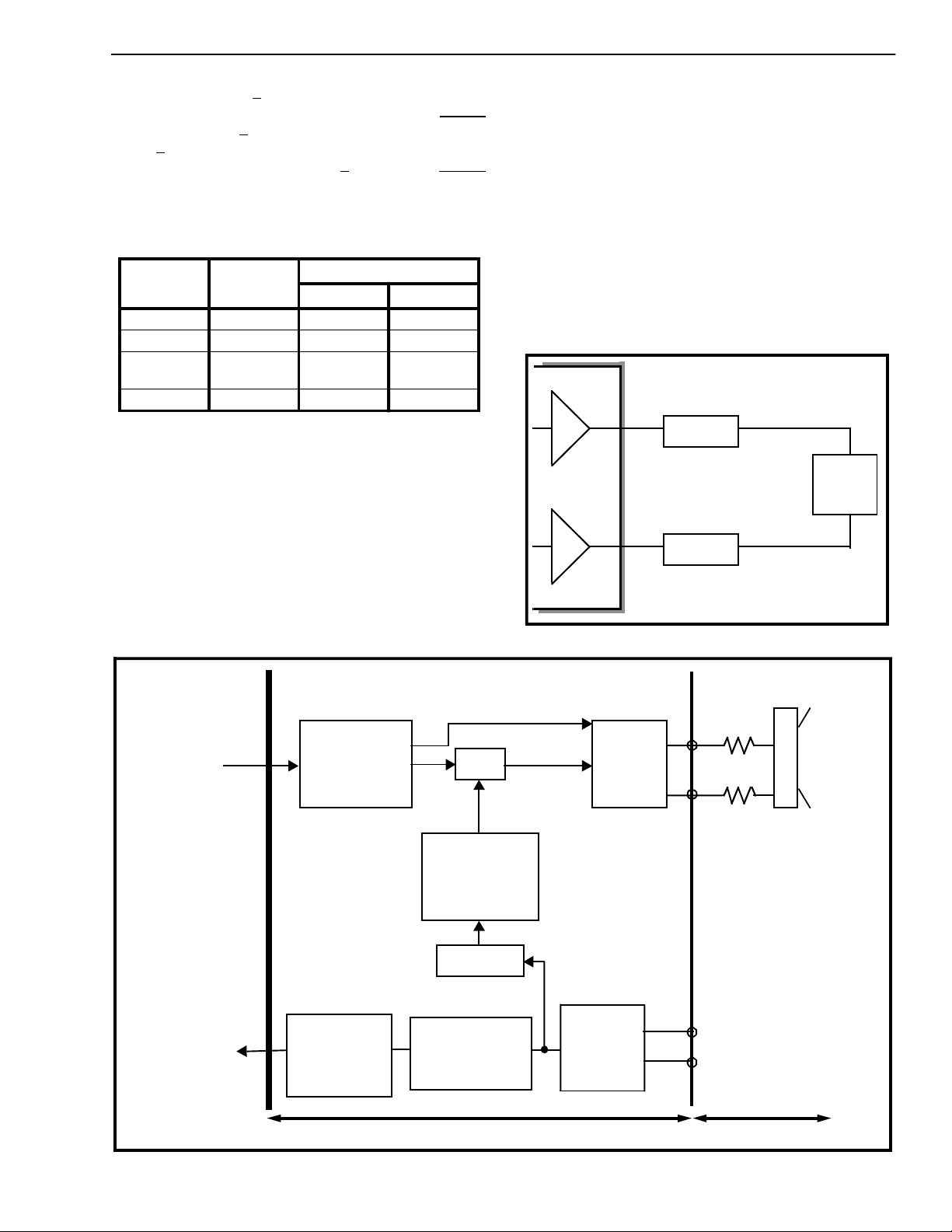
feature is disabled by default. Figure 3 depicts the
nominal half-channel and side-tone gains for the
MT9160.
In the event of PWRST
, the MT9160 defaults such
that the side-tone path is off, all programmable gains
are set to 0dB and CCITT µ-Law is selected. Further,
the digital port is set to SSI mode operation at 2048
kb/s and the FDI and driver sections are powered up.
(See Microport section.)
The internal architecture is fully differential to provide
the best possible noise rejection as well as to allow a
wide dynamic range from a single 5 volt supply
The receive filter is designed to meet CCITT G.714
specifications. The nominal gain for this filter is 0 dB
(gain control = 0dB). Gain control allows t he output
signal to be attenuated up to 7 dB. Filter response is
peaked to compensate for the sinx/x attenuation
caused by the 8 kHz sampling rate.
Side-tone is derived from the input of the Tx filter and
is not subject to the gain control of the Tx filter
section. Side-tone is summed into the receive
handset transducer driver path after the Rx filter gain
control section so that Rx gain adjustment will not
affect side-tone levels. The side-tone path may be
enabled/disabled with the gain control bits located in
Gain Control Register 2 (address 01h).
Transmit and receive filter gains are controlled by the
TxFG
-TxFG2 and RxFG0-RxFG2 control bits,
0
respectively. These are located in Gain Control
Register 1 (address 00h). Transmit filter gain is
adjustable from 0 dB to +7 dB and receive filter gain
from 0dB to -7 dB, both in 1 dB increments.
Side-tone filter gain is controlled by the STG
-STG
0
control bits located in Gain Control Register 2
(address 01h). Side-tone gain is adjustable from
-9.96 dB to +9.96 dB i n 3 .3 2 dB in c r em en ts .
2
Intel® and MCS-51® are registered trademarks of Intel Corporation
Motorola® and SPI® are registered trademarks of Motorola Corporation
National® and Microwire® are trademarks of National Semiconductor Corporation
7-80
Page 5
Preliminary Information MT9160
Companding law selection for the Filter/Codec is
provided by the A/µ
companding control bit while
the coding scheme is controlled by the Smag/CCITT
control bit. The A/µ control bit is logically OR’ed with
the A/µ
controllerless modes. Both A/µ
pin providing access in both controller and
and Smag/CCITT
reside in Control Register 2 (address 04h). Table 1
illustrates th es e ch o ice s.
Code
+ Full Scale 1111 1111 1000 0000 1010 1010
+ Zero 1000 0000 1111 1111 1101 0101
-Zero
(quiet code)
- Full Scale 0111 1111 0000 0000 0010 1010
Sign/
Magnitude
0000 0000 0111 1111 0101 0101
CCITT (G.7 11)
µ-Law A-Law
Ta ble 1
Transducer Interfaces
Standard handset transducer interfaces are provided
by the MT9160. These are:
Control of this gain is provided by the TxINC
control bit (G ain Co ntrol reg iste r 1, add ress 0 0h).
• The handset speaker outputs (receiver), pins
HSPKR+/HSPKR-.This internally compensated
fully differ ential outp ut driver is ca pab le of d rivi ng
the load sh own in Figu re 4. Th e nominal handse t
receive path gain may be adjusted to either 0 dB,
-6 dB or -12 d B. Control of this gai n is provided
by the Rx INC contro l bit (Gain C ontrol re gister 1,
address 00h ). This gain adj ustment is in addition
to the programmable gain provided by the receive
filter.
HSPKR +
75 Ω
150 ohm
MT9160
75 Ω
load
(speaker)
• The handset microphone inputs (transmitter),
pins M+/M-. The nominal transmit amplifier gain
may be adjusted to either 6.0 dB or 15.3 dB.
Serial Port
PCM
D
in
Filter/Codec and Transducer Interface
Receive
Filter Gain
0 to -7 dB
(1 dB steps)
-6 dB
Side-tone
-9.96 to
+9. 96 dB
(3.32 dB steps)
-11 dB
Default Bypass
HSPKR -
Figure 4 - Handset Speaker Driver
HSPKR +
75Ω
HSPKR -
75Ω
Default Side-tone off
-6.0 dB or
0 dB
Receiver
Driver
Handset
Receiver
(150Ω)
PCM
D
out
Transmit Filter
Transmit Fil te r
Gain
Gain
0 to +7 dB
0 to +7 dB
(1 dB steps)
(1 dB steps)
Transmit Gain
-0.37 dB or 8.93 dB
INTERNAL TO DEVICE
Transmit
Gain
6.37 dB
Figure 3 - Audio Gain Partitioning
M+
Transmitter
Micropho ne
M-
EXTERNAL TO DEVICE
7-81
Page 6

MT9160 Preliminary Information
Microport
The serial microport, compatible with Intel MCS-51
(mode 0), Motorola SPI (CPOL=0,CPHA=0) and
National Semiconductor Microwire specifications
provides access to all MT9160 internal read and
write registers. This microport consists of a transmit/
receive data pin (DATA1), a receive data pin
(DATA2), a chip select pin (CS
data clock pin (SCLK). For D-channel contention
control, in ST-BUS mode, this interface provides an
open-drain interrupt output (IRQ
The microport dynamically senses the state of the
serial clock (SCLK) each time chip select becomes
active. The device then automatically adjusts its
internal timing and pin configuration to conform to
Intel or Motorola/National requirements. If SCLK is
high during chip select activation then Intel mode 0
timing is assumed. The DATA1 pin is defined as a
bi-directional (transmit/receive) serial port and
DATA2 is internally disconnected. If SCLK is low
during chip select activation then Motorola/National
timing is assumed. Motorola processor mode
CPOL=0, CPHA=0 must be used. DATA1 is defined
as the data transmit pin while DATA2 becomes the
data receive pin. Although the dual port Motorola
controller configuration usually supports full-duplex
communication, only half-duplex communication is
possible in the MT9160. The micro must discard
non-valid data which it clocks in during a valid write
transfer to the MT9160. During a valid read transfer
from the MT9160 data simultaneously clocked out by
the micro is ignored by the MT9160.
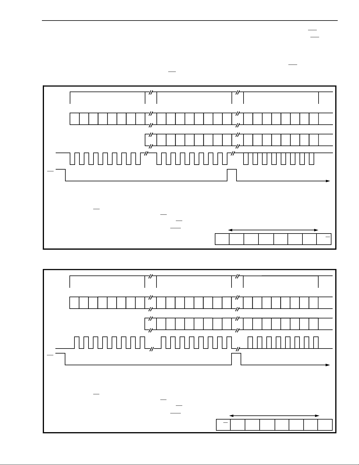
All data transfers through the microport are two-byte
transfers requiring the transmission of a Command/
Address byte followed by the data byte written or
read from the addressed register. CS
asserted fo r th e duration of this t wo - by te t ra n sfer. As
shown in Figures 5 and 6 the falling edge of CS
indicates to the MT9160 tha t a microport tran sfer is
about to begin. The first 8 clock cycles of SCLK after
the falling edge of CS
Command/Address byte from the microcontroller.
The Command/Address byte contains information
detailing whether the second byte transfer will be a
read or a write operation and at what address. The
next 8 clock cycles are used to transfer the data byte
between the MT9160 and the microcontroller. At the
end of the two-byte transfer CS
to terminate the session. The rising edge of CS
tri-state the output driver of DATA1 which will remain
tri-stated as long as CS
Intel processors utilize least significant bit first
transmission while Motorola/National processors
employ most significant bit first transmission. The
MT9160 microport automatically accommodates
are always used to receive the
is high.
) and a synchronous
).
must remain
is brought high again
will
these two schemes for normal data bytes. However,
to ensure decoding of the R/W
information, the Command/Address byte is defined
differently for Intel operation than it is for Motorola/
National operation. Refer to the relative timing
diagrams of Figures 5 and 6.
Receive data is sampled on the rising edge of SCLK
while transmit data is made available concurrent with
the falling edge of SCLK.
Flexible Di gital Interf ace
A serial link is required to transport data between the
MT9160 and an external digital transmission device.
The MT9160 utilizes the ST-BUS architecture
defined by Mitel Semiconductor but also supports a
strobed data interface found on many standard
Codec devices. This interface is commonly referred
to as Synchronous Serial Interface (SSI). The
combination of ST-BUS and SSI provides a Flexible
Digital Interface (FDI) capable of supporting all Mitel
basic rate transmission devices as well as many
other 2B+D transceivers.
The required mode of operation is selected via the
CSL2-0 control bits (Control Register 2, address
04h). Pin definitions alter dependent upon the
operational mode selected, as described in the
following subsections as well as in the Pin
Description tables.
Quiet Code
The FDI can be made to send quiet code to the
decoder and receive filter path by setting the RxMute
bit high. Likewise, the FDI will send quiet code in the
transmit path when the TxMute bit is high. Both of
these control bits reside in Control Register 1 at
address 03h. When either of these bits are low their
respective paths function normally. The -Zero entry
of Table 1 is used for the quiet code definition.
ST-BUS Mode
The ST-BUS consists of output (DSTo) and input
(DSTi) serial data streams, in FDI these are named
Dout and Din respectively, a synchronous clock input
signal CLOCKin (C4i
(F0i
). These signals are direct connections to the
corresponding pins of Mitel basic rate devices. The
CSL2, CSL1 and CSL0 bits are set to 1 for ST-BUS
operation.
), and a framing pulse input
and address
7-82
Page 7
Preliminary Information MT9160
The data streams operate at 2048 kb/s and are Time
Division Multiplexed into 32 identical channels of 64
kb/s bandwidth. A frame pulse (a 244 nSec low going
pulse) is used to parse the continuous serial data
streams into the 32 channel TDM frames. Each
frame has a 125 µSecond period translating into an 8
kHz frame rate. A valid frame begins when F0i
COMMAND/ADDRESS DATA INPUT/OUTPUT COMMAND/ADDRESS:
DATA 1
RECEIVE
DATA 1
TRANSMIT
SCLK
CS
➀ Delays due to internal processor timing which are transparent.
② Th e MT9160:-latches received data on the rising edge of SCLK.
➂ The falling edge of CS
subsequent byte is always data until terminated via CS
➃ A new COMMAND/ADDRESS byte may be loaded only by CS
➄ The COMMAND/ADDRESS b yte contains:
D0D1D2D3D4D5D6D
②
➂
-outputs transmit data on the falling edge of SCLK.
indicates that a COMMAND/ADDRESS byte will be transmitted from the microprocessor. The
➄
➀
D0D1D2D3D4D5D6D
7
D0D1D2D3D4D5D6D
1 bit - Read/Write
3 bits - Addressing Data
4 bits - Unused
is
returning high.
logic low coincident with a falling edge of C4i
to Figure 11 for detailed ST-BUS timing. C4i
frequency (4096 kHz) which is twice the data rate.
This clock is used to sample the data at the 3/4
bit-cell position on DSTi and to make data available
on DSTo at the start of the bit-cell. C4i
is also used to
clock the MT9160 internal functions (i.e., Filter/
➃
D0D1D2D3D4D5D6D
D0D1D2D3D4D5D6D
XX
7
7
➃
➂
cycling high then low again.
D
7
XX A2A1A0R/W
➀
. Refer
has a
7
7
D
0
Figure 5 - Serial Port Relative Timing for Intel Mode 0
COMMAND/ADDRESS DATA INPUT/OUTPUT COMMAND/ADDRESS:
DATA 2
RECEIVE
DATA 1
TRANSMIT
SCLK
CS
➀Delays due to internal processor timing which are transparent .
② The MT9160:-latches received data on the rising edge of SCLK.
➂ The falling edge of CS
subsequent byte is always data until terminated via CS
➃ A new COMMAND/ADDRESS byte may be loaded only by CS
➄ The COMMAND/ADDRESS byte contains:
D7D6D5D4D3D2D1D
②
➂
-outputs transmit data on the falling edge of SCLK.
indicates that a COMMAND/ADDRESS byte will be transmitted from the microprocessor. The
➄
➀
D7D6D5D4D3D2D1D0D7D6D5D4D3D2D1D
0
D7D6D5D4D3D2D1D0D7D6D5D4D3D2D1D
returning high.
1 bit - Read/Write
3 bits - Addressing Data
4 bits - Unused
➃
cycling high then low again.
D
7
R/W XA
➀
➂
➃
XX
A
2
1
0
0
D
0
A
X
0
Figure 6 - Serial Port Relative Timing for Motorola Mode 00/National Microwire
7-83
Page 8
MT9160 Preliminary Information
125 µ s
F0i
DSTi,
DST o
CHANNEL 0
D-channel
LSB first
for D-
Channel
CHANNEL 1
C-channel
CHANNEL 2
B1-channel
MSB first for C, B1- & B2-
Channels
CHANNEL 3
B2-channel
Figure 7 - ST-BUS Channel Assignment
Codec, Digital gain and tone generation) and to
provide the channel timing requirements.
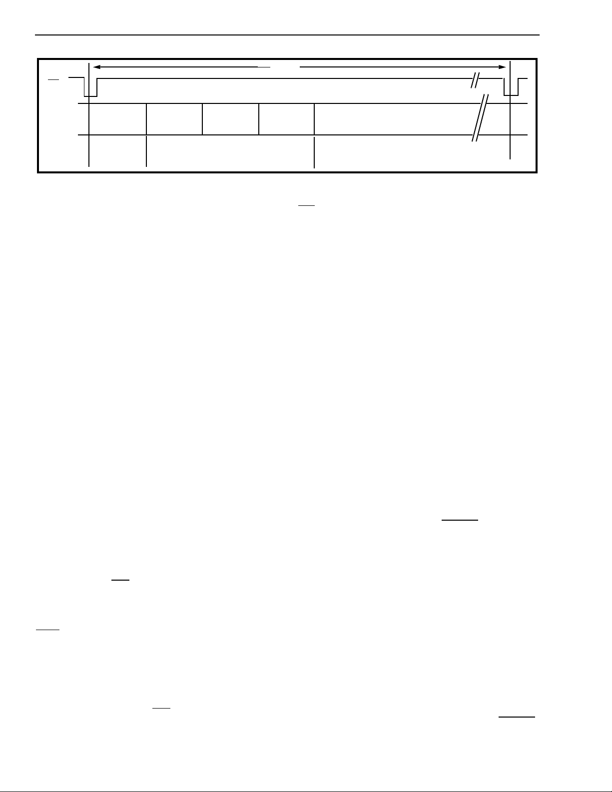
The MT9160 uses only the first four channels of the
32 channel frame. These channels are always
defined, beginning with Channel 0 after the frame
pulse, as shown in Figure 7 (ST-BUS channel
assignments).
The first two (D & C) Channels are enabled for use
by the DEN and CEN bits respectively, (Control
Register 2, address 04h). ISDN basic rate service
(2B+D) defines a 16 kb/s signalling (D) Channel. The
MT9160 supports transparent access to this
signalling channel. ST-BUS basic rate transmission
devices, which may not employ a microport, provide
access to their internal control/status registers
through the ST-BUS Control (C) Channel. The
MT9160 supports microport access to this
C-Channel.
DEN - D-Channe l
In ST-BUS mode ac cess to the D -Channel ( transmit
and receive) data is provided through an 8-bit read/
write register (address 06h). D-Channel data is
accumulated in, or transmitted from this register at
the rate of 2 bits/frame for 16 kb/s operation (1 bit/
frame for 8 kb/s operation). Since the ST-BUS is
asynchronous, with respect to the microport, valid
access to this register is controlled through the use
of an interrupt (IRQ
) output. D-Channel access is
enabled via the (DEn) bit.
DEn:
When 1, ST-BUS D-channel data (1 or 2 bits/frame
depending on the state of the D8 bit) is shifted into/
out of the D-channel (READ/WRITE) register.
CHANNELS 4-31
Not Used
D8:
When 1, D-Channel data is shifted at the rate of 1 bit/
frame (8 kb/s).
When 0, D-Channel data is shifted at the rate of 2
bits/frame ( 1 6 kb/s default).
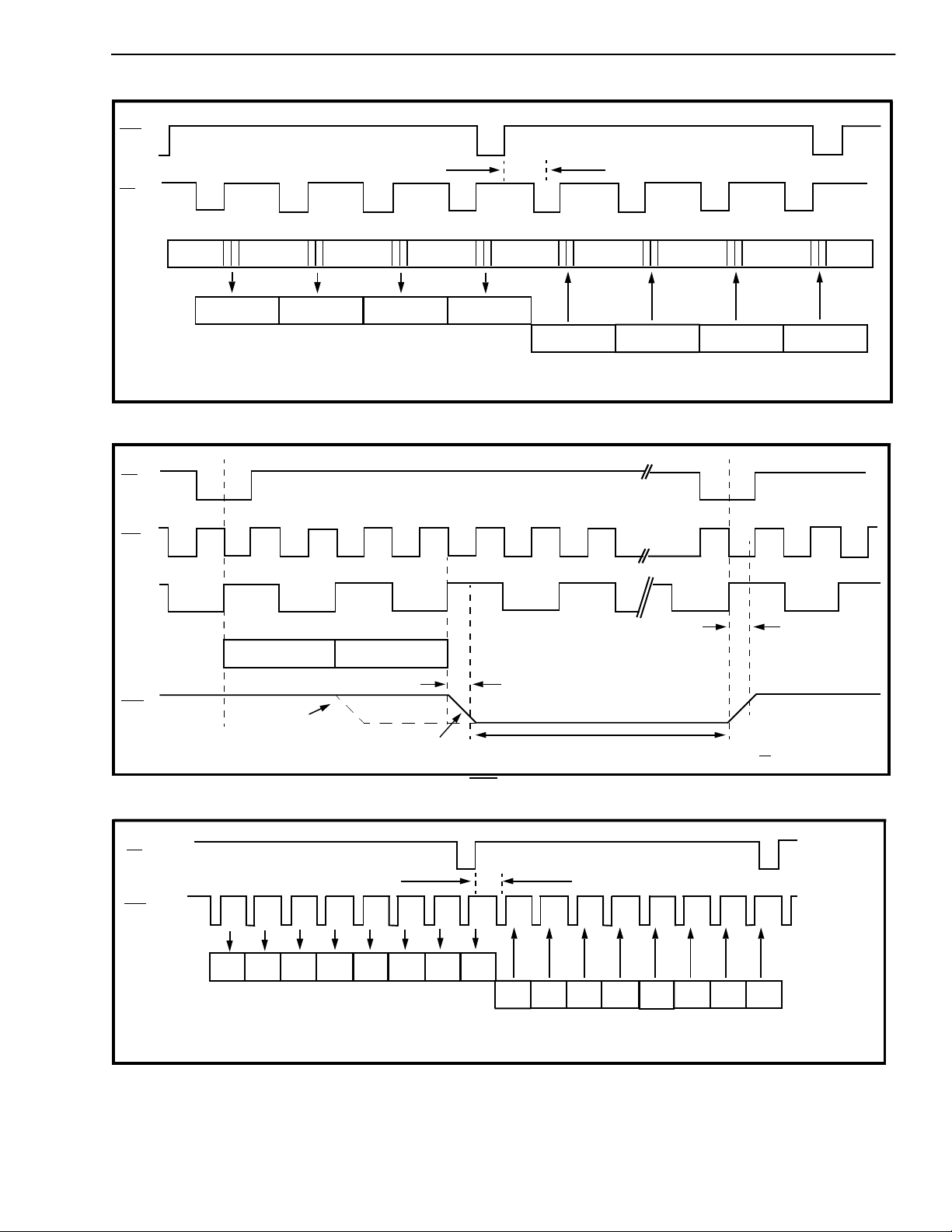
16 kb/s D-Channel operation is the default mode
which allows the microprocessor access to a full byte
of D-Channel information every fourth ST-BUS
frame. By arbitrarily assigning ST-BUS frame n as
the reference frame, during which the
microprocessor D-Channel read and write operations
are performed, then:
(a) A microport read of address 04 hex will result in a
byte of data being extracted which is composed of
four di-bits (designated by roman numerals I,II,III,IV).
These di-bits are composed of the two D-Channel
bits received during each of frames n, n-1, n-2 and
n-3. Referring to Fig. 8a: di-bit I is mapped from
frame n-3, di-bit II is mapped from frame n-2, di-bit III
is mapped from frame n-1 and di-bit IV is mapped
from frame n.
The D-Channel read register is not preset to any
particular value on power-up (PWRST
) or software
reset (RST).
(b) A microport write to Address 04 he x will result in
a byte of data being loaded which is composed of
four di-bits (designated by roman numerals I, II, III,
IV). These di-bits are destined for the two D-Channel
bits transmitted during each of frames n+1, n+2, n+3,
n+4. Referring to Fig. 8a: di-bit I is mapped to frame
n+1, di-bit II is mapped to frame n+2, di bit III is
mapped to frame n+3 and di bit IV is mapped to
frame n+4.
When 0, the receive D-channel data (READ) is still
shifted into the proper register while the DSTo
D-channel timeslot and IRQ
outputs are tri-stated
(default).
7-84
If no new data is written to address 04 hex , the
current D-channel register contents will be
continuously re-transmitted. The D-Channel write
register is preset to all ones on power-up (PWRST
or softwa re r es e t ( RS T).
)
Page 9
Preliminary Information MT9160
IRQ
Micropo rt Rea d/Wri te A c cess
FP
DSTo/
DSTi
n-3 n-2 n-1 n n+1 n+2 n+3 n+4*
Di-bit Group
Receive
D-Channel
I
D0 D1
No preset value
II
D2 D3
D4
III
D5
* note that fram e n+4 is equ ival en t to frame n of the next cycle.
Figure 8a - D-Channel 16 kb/s Operation
FP
C4i
C2
DSTo/
DSTi
IRQ
D0
8 kb/s operation
D1
16 kb/s operation
IV
D6
D7
Di-bit Group
Transmit
D-Channel
t
if
D0 D1ID2
II
Power-up reset to 1111 1111
=500 nsec max
Microport Read/Write Access
D3
III
D4
D5
D6 D7
t
=500 nsec max
ir
R
pullup
Reset coincident with
Read/Write of Address 04 Hex
or next FP
, whichever occurs first
IV
= 10 k
FP
IRQ
Di-bit Group
Receive
D-Channel
Figure 8b - IRQ
n-7 n-6 n-5 n-4 n-3 n-2 n-1 n n+1
IID1IIID2IVD3VD4VID5VIID6VIII
I
D0
No preset value
Di-bit Group
Transmit
D-Channel
Timing Diagram
D7
Figure 8c - D-Channel 8 kb/s Operation
Microport Read/Write Access
I
D0
n+2
IID1IIID2IV
n+3
n+4
D3
Power-up reset to 1111 1111
n+5
VID5VIID6VIII
V
D4
n+6
n+7 n+8
D-Channel
D7
7-85
Page 10

MT9160 Preliminary Information
An interrupt output is provided (IRQ) to synchronize
microprocessor access to the D-Channel register
during valid ST-BUS periods only. IRQ
every fourth (eighth in 8 kb/s mode) ST-BUS frame
at the beginning of the third (second in 8 kb/s mode)
ST-BUS bit cell period. The interrupt will be removed
following a microprocessor Read or Write of Address
04 hex or upon encountering the following frames’s
FP
input, whichever occurs first. To ensure
D-Channel data integrity, microport read/write
access to Address 04 hex must occur before the
following fra me p u l se . Se e F igu r e 8b for timing.
8 kb/s operation expands the interrupt to every eight
frames and processes data one-bit-per-frame.
D-Channel register data is mapped according to
Figure 8c.
will occur
CEn - C-Chann el
Channel 1 conveys the control/status information for
the Layer 1 transceiver. C-Channel data is
transferred MSB first on the ST-BUS by the MT9160.
The full 64 kb/s bandwidth is available and is
assigned according to which transceiver is being
used. Consult the data sheet for the selected
transceiver for its C-Channel bit definitions and order
of bit tran s fe r.
When CEN is high, data written to the C-Channel
register (address 05h) is transmitted, most
significant bit first, on DSTo. On power-up reset
(PWRST
C-Channel bits default to logic high. Receive
C-Channel data (DSTi) is always routed to the read
register regardless of this control bit's logic state.
When low, data transmission is halted and this
timeslot i s tri-stated o n D S To.
) or software reset (Rst, address 03h) all
B1-Channe l and B 2-Cha nne l
SSI Mode
The SSI BUS consists of input and output serial data
streams named Din and Dout respectively, a Clock
input signal (CLOCKin), and a framing strobe input
(STB). The frame strobe must be synchronous with,
and eight cycles of, the bit clock. A 4.096 MHz
master clock is also required for SSI operation if the
bit clock is less than 512 kHz. The timing
requirements for SSI are shown in Figures 12 & 13.
In SSI mode the MT9160 supports only B-Channel
operation. The internal C and D Channel registers
used in ST-BUS mode are not functional for SSI
operation. The control bits TxBSel and RxBSel, as
described in the ST-BUS section, are ignored since
the B-Channel timeslot is defined by the input STB
strobe. Hence, in SSI mode transmit and receive
B-Channel data are always in the channel defined by
the STB input.
The data strobe input STB determines the 8-bit
timeslot used by the device for both transmit and
receive data. This is an active high signal with an 8
kHz repetition rate.
SSI operation is separated into two categories based
upon the data rate of the available bit clock. If the bit
clock is 512 kHz or greater then it is used directly by
the internal MT9160 functions allowing synchronous
operation. If the available bit clock is 128 kHz or 256
kHz, then a 4096 kHz master clock is required to
derive clocks for the internal MT9160 functions.
Applications where Bit Clock (BCL) is below 512 kHz
are designated as asynchronous. The MT9160 will
re-align its internal clocks to allow operation when
the external master and bit clocks are asynchronous.
Control bits CSL2, CSL1 and CSL0 in Control
Register 2 (address 04h) are used to program the bit
rates.
Channels 2 and 3 are the B1 and B2 channels,
respectively. B-channel PCM associated with the
Filter/Codec and transducer audio paths is selected
on an independent basis for the transmit and receive
paths. TxBSel and RxBSel (Control Register 1,
address 03h) are used for this purpose.
If no valid transmit path has been selected then the
timeslot output on DSTo is tri-stated (see PDFDI and
PDDR control bits, Control Register 1 address 03h).
7-86
For synchronous operation data is sampled, from
Din, on the falling edge of BCL during the time slot
defined by the STB input. Data is made available, on
Dout, on the rising edge of BCL during the time slot
defined by the STB input. Dout is tri-stated at all
times when STB is not true. If STB is valid but PDFDI
and PDDR are not true, then quiet code will be
transmitted on Dout during the valid strobe period.
There is no frame delay through the FDI circuit for
synchronous operation.
For asynchronous operation Dout and Din are as
defined for synchronous operation except that the
allowed output jitter on Dout is larger. This is due to
the resynchronization circuitry activity and will not
Page 11
Preliminary Information MT9160
affect operation since the bit cell period at 128 kb/s
and 256 kb/s is relatively large. There is a one frame
delay through the FDI circuit for asynchronous
operation. Refer to the specifications of Figures 12
& 13 for both synchronous and asynchronous SSI
timing.
PWRST
While the MT9160 is held in PWRST
/Software Res et (Rs t)
no device
control or functionality is possible. While in software
reset (Rst=1, address 03h) only the microport is
functional. Software reset can only be removed by
writing Rst logic low or by setting the PWRST
After Power-up reset (PWRST
) or software reset
pin.
(Rst) all control bits assume their default states;
µ-Law functionality, usually 0 dB programmable
gains as well as the device powered up in SSI mode
2048 kb/s operation with Dout tri-stated while there
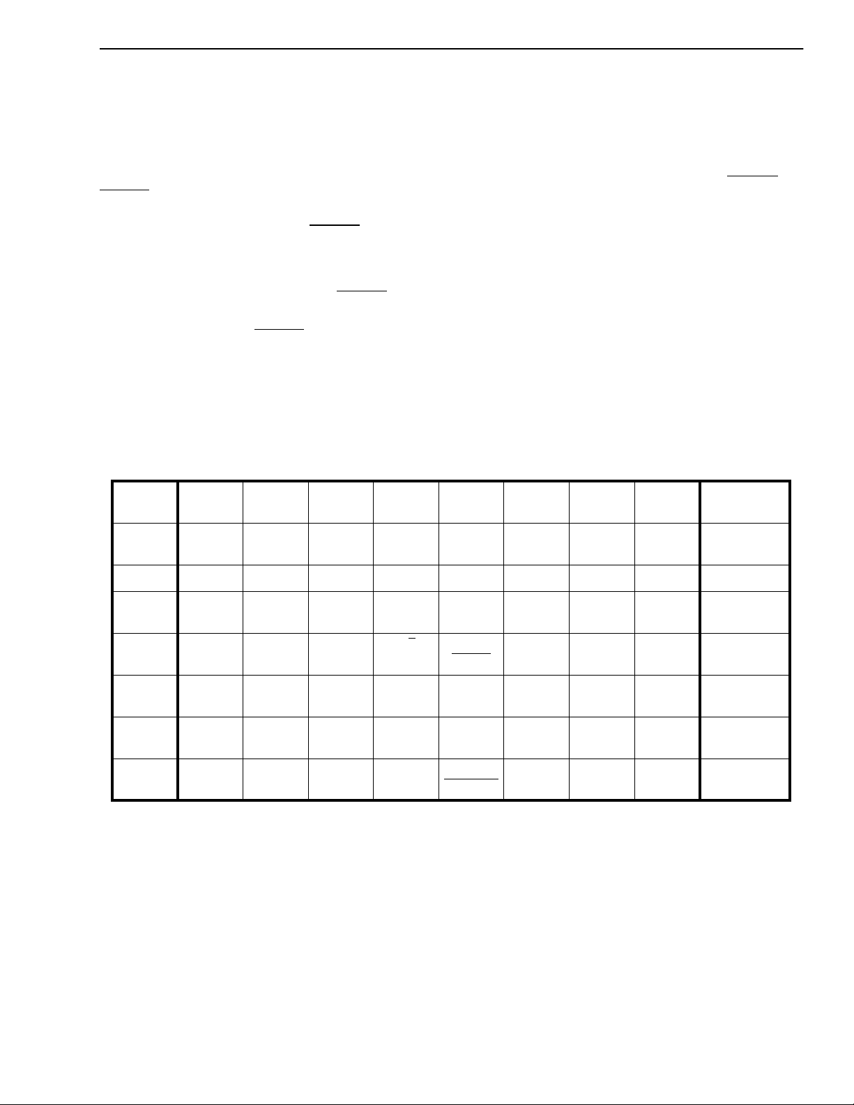
5V Multi-featured Codec Register Map
is no strobe active on STB. If a valid strobe is
supplied to STB, then Dout will be active, during the
defined channel.
To attain complete power-down from a normal
operating condition, write PDFDI = 1 and PDDR = 1
(Control Register 1, address 03h) or put PWRST
pin
low.
00 RxINC RxFG
RxFG
2
RxFG
1
TxINC TxFG
0
TxFG
2
TxFG0Gain C on trol
1
Register 1
01-----STG
STG
2
STG
1
Gain C on trol
0
Register 2
02-------DrGainPath Control
03 PDFDI PDDR RST - T
Mute RxMute TxBsel RxBsel Control
x
Register 1
04 CEN DEN D8 A/µ
05 C
7
C
6
C
5
C
4
Smag/
CCITT
C
3
CSL
C
CSL
2
CSL
1
0
Control
Register 2
2
C
1
C
0
C-Channel
Register
06 D
7
D
6
D
5
D
4
D
3
D
2
D
1
D
0
D-Channel
Register
07----PCM/
loopen - - Loop Back
ANALOG
7-87
Page 12
MT9160 Preliminary Information
Register Summary
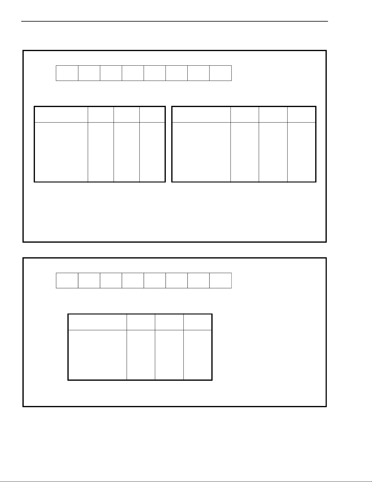
Gain Control Register 1 ADDRESS = 00h WRITE/READ V ERIFY
Power Reset Value
RxINC
RxFG
RxFG1RxFG
2
0
TxINC
TxFG2TxFG1TxFG
76543210
0
1000 0000
Receive Gain
Setting (dB)
(default) 0
-1
-2
-3
-4
-5
-6
-7
RxFGn = Receive Filter Gain bit n
RxINC: When high, the receiver driver nominal gain is set to 0 dB. When low, this gain is -6.0 dB.
TxINC: When high, the transmit amplifier nominal gain is set to 15.3 dB. When low, this gain is 6.0 dB.
RxFG
0
0
0
0
1
1
1
1
RxFG
2
0
0
1
1
0
0
1
1
RxFG
1
0
0
1
0
1
0
1
0
1
Transmit Gain
Setting (dB)
(default) 0
1
2
3
4
5
6
7
= Transmit Filter Gain bit n
TxFG
n
TxFG
0
0
0
0
1
1
1
1
TxFG
2
0
0
1
1
0
0
1
1
TxFG
1
0
0
1
0
1
0
1
0
1
Gain Control Register 2 ADDRESS = 01h WRITE/READ V ERIFY
Power Reset Value
---- STG
-
STG1STG
2
0
XXXX X000
76543210
Side-tone Gain
Setting (dB)
(default) OFF
-9.96
-6.64
-3.32
0
3.32
6.64
9.96
= Side-tone Gain bit n
STG
n
STG
0
0
0
0
1
1
1
1
2
STG
0
0
1
1
0
0
1
1
1
STG
Note: Bits marked "-" are reserved bits and should be written with logic "0"
7-88
0
0
1
0
1
0
1
0
1
Page 13
Preliminary Information MT9160
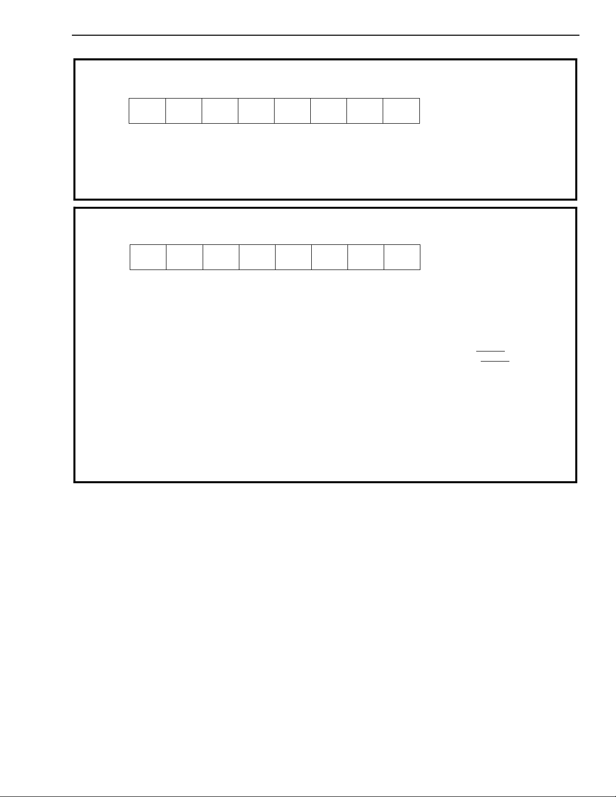
Path Control
---
-
-
--
ADDRESS = 02h WRITE/READ VER IFY
Power Reset Value
DrGain
XX00 0000
76543210
DrGain When high, the receiver driver gain is set to -6 dB, with sidetone.
When low, the receiver driver gain is set to 0 dB, with no sidetone.
Control Reg ister 1
PDFDI P DDR TxBsel RxBselRst
_
TxMute RxMute
ADDRESS = 03h WRITE/READ VER IFY
Power Reset Value
000 0 00 00
76543210
PDFDI When high, the FDI PLA and the Filter/ Cod ec are po were d down. Wh en low, the FDI is active (de fault ).
PDDR Whe n high, the ear driver and Fil ter/Codec are p owered down. In addition, in ST-BUS mode, the sele cted output
Rst When high, a software reset occurs performing the sam e function as the hardw are reset (PWRST
TxMut e When hig h the tra nsm it PCM st ream is inter rupte d and rep lace d with qu iet cod e; thu s for cing the outpu t code in to a
RxMute When high the received PCM stream is interrupted and rep laced with quiet code; thus forci ng the receive path into a
TxBsel When high, the transm it B2 cha nnel is functio na l in ST -BUS mo de. Wh en lo w, the t ransmi t B1 channe l is f unction al in
RxBsel When high, the re ceive B2 channel is functiona l in ST-B US mode. When low, t he rece ive B1 cha nnel is functi onal in
channel is tri-stated. In SSI mode the PCM output code will be -zero code during the valid strobe period. The output will
be tri-stated outside of the valid strobe and for the whole frame if no strobe is supplied. When low, the driver and Filter/
Codec are active if PDFDI is low (default).
microport is no t a ffect ed. A software reset ca n be remo ve d only by writ in g this b it low or b y a P WRST
reset condition is removed.
mute state (only the output code is muted, the transmit microphone and transmit Filter/Codec are still functional). When
low the full transmit path functions normally (default).
mute state. When low the full receive path functions norm al ly (default).
ST-BUS mode. Not used in SSI mode.
ST-BUS mode. Not used in SSI mode.
) except that the
. When low, the
Note: Bits marked "-" are reserved bits and should be written with logic "0"
7-89
Page 14
MT9160 Preliminary Information
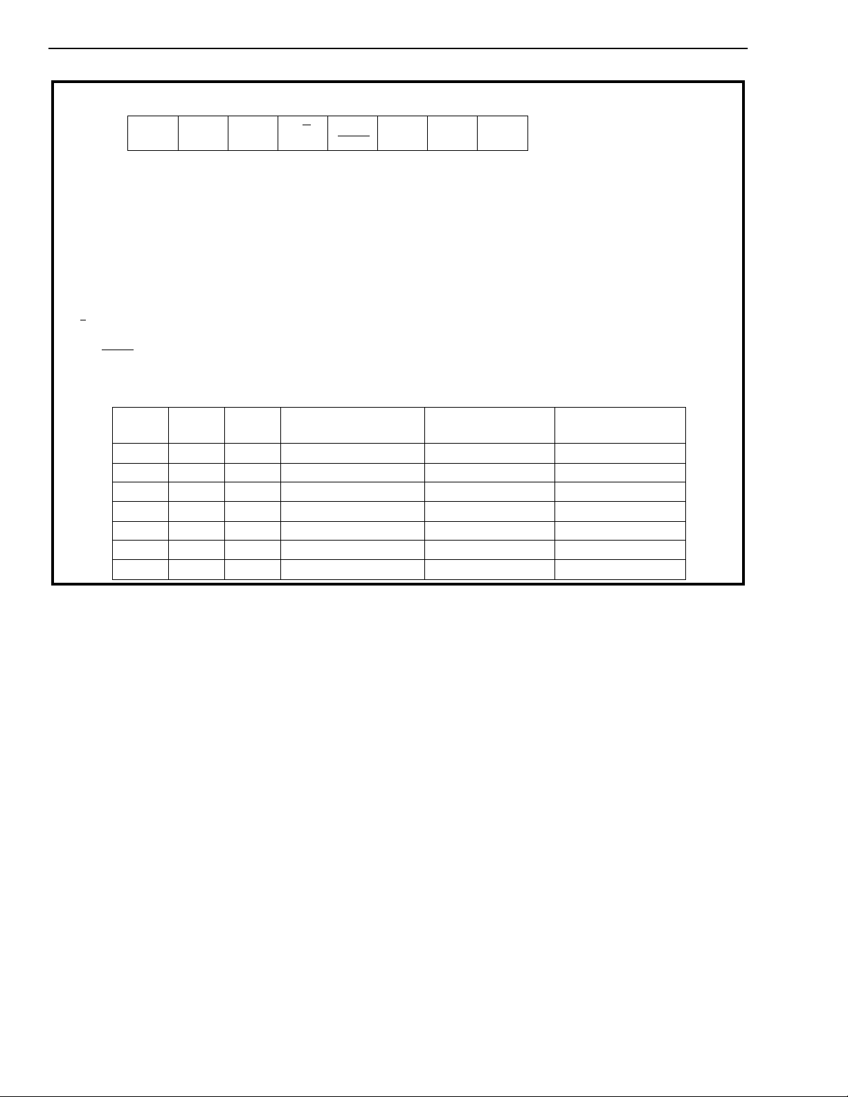
Control Register 2 ADDRESS = 04h WRITE/READ V ERIFY
Power Reset Value
0000 0010
CEn DEn
D8
A/µ
Smag/
CCITT
CSL
CSL
2
CSL
1
0
76543210
CEn When high, data written into the C-Channel register (address 05h) is transmitted during channel 1 on DSTo. When
DEn When high, data writte n int o the D-Cha n nel Re gister (a ddress 06 h) is tra nsm itted (2 bits/f rame ) during ch annel 0
D8 When high, D-channel operates at 8kb/s. When low, D-cha nnel operates at 16kb/s (defau lt).
A/µ
Smag/CCITT
CSL
low, the channel 1 timeslot is tri-stated on DSTo. Ch annel 1 data received on DSTi is read via the C-Channel
register (address 05h) regardl ess of the state o f CEn . This control bit has sign ifican ce only for ST-B US oper ation
and is ignored for SSI operation.
on DSTo. The rem aining six bits of the D-Ch annel carry no information. W hen low, the channel 0 time slot is
completely tri-stat ed on DSTo . Ch an nel 0 da ta recei ve d on DSTi is read via the D-Ch anne l reg ister r eg ardle ss of
the state of DEN. This control bit has significance only for ST-BUS mode and is ignored for SSI operation.
When high, A-Law encoding/decoding is selected for the MT9160. When low, µ-Law encoding/decoding is
selected.
When high, sign-magnitude code assignment is selected for the Codec input/output. When low, CCITT code
assignment is sele cted for the Codec in put/output; true sig n, inverted magnitu de (µ-Law) or true sign, alternate
digit inversion (A-Law).
CSL
2
1 1 1 not applicable 4096 ST-BUS
100 128 4096 SSI
1 0 1 256 4096 SSI
000 512 512 SSI
001 1536 1536 SSI
010 2048 2048 SSI (default)
011 4096 4096 SSI
CSL
1
External bit Clock Rate
0
(kHz)
CLOCKin (kHz) Mode
Note: Bits marked "-" are reserved bits and should be written with logic "0"
7-90
Page 15
Preliminary Information MT9160
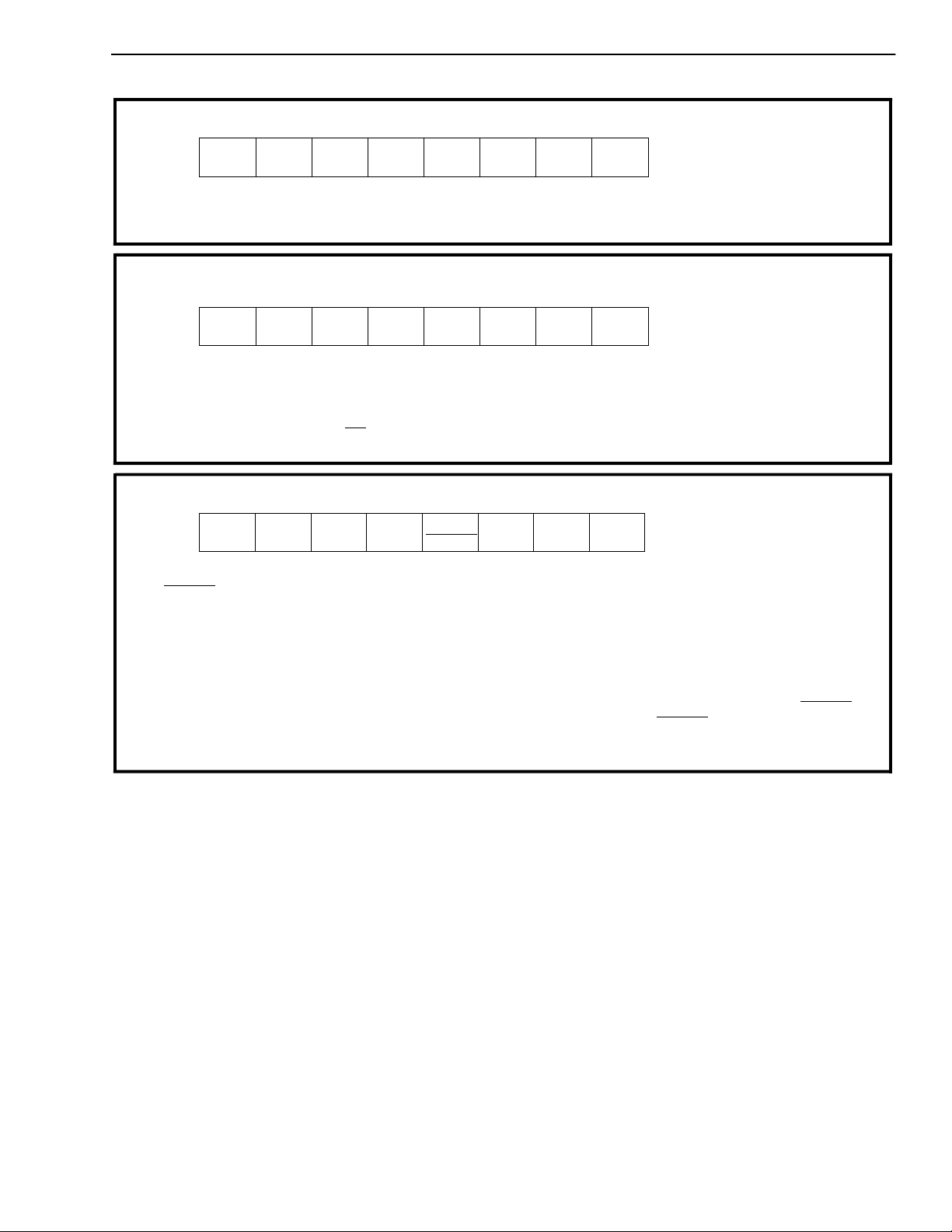
C-Channel Register ADDRESS = 05h WRITE/READ
Power Reset Value
C7 C6 C5 C4 C2 C1 C0C3
76543210
Micro-port access to the ST-BUS C-Channel information read and write
1111 1111- write
XXXX XXXX - read
D-Channel Register
D7 D6 D5 D4 D2 D1 D0
D3
ADDRESS = 06h WRITE/READ
Power Reset Value
1111 1111- write
XXXX XXXX - read
76543210
D7-D0 Data wri tten to this register will be transmitted every frame, in channel 0, if the DEn control bit is set (address 04h) .
Loopback Register
Received D-Cha nn el data is val id, re gard less o f the st ate o f DEn. T hese b its a re va lid for ST-BU S mod e on ly and are
accessible only when IRQ
indicates valid access.
ADDRESS = 07h WRITE/READ VERI FY
--
PCM/
--
-
ANALOG
loopen
-
Power Reset Value
XXXX 0000
76543210
PCM/ANALOG This control bit functions only when loopen is set high. It is ignored when loopen is low.
For loopback oper ati on whe n thi s bit is high , th e device is co nfig ure d for d ig ital-t o-d ig ital l oopback operation. Data on
Din is looped back to Dout without conversio n to the analog doma in. However, the receive D/A path (fro m Din to
HSPKR
±) still functions. When low, the device is configured for analog-to-analog operation. An analog input signal at
M
± is looped back to the SPKR± o utput s throu gh the A/D an d D/A cir cuits as wel l as thro ugh the norm al tra nsm it A/D
path (from M
loopen When high, loopback ope ration is enabled and the loopba ck type is governed by the stat e of the PCM/ANALOG bit.
When low, loopbac ks are disabled, the device operates nor mall y and the PCM/ANALOG
± to Dout).
bit is ignored.
Note: Bits marked "-" are reserved bits and should be written with logic "0"
7-91
Page 16
MT9160 Preliminary Information
Applications
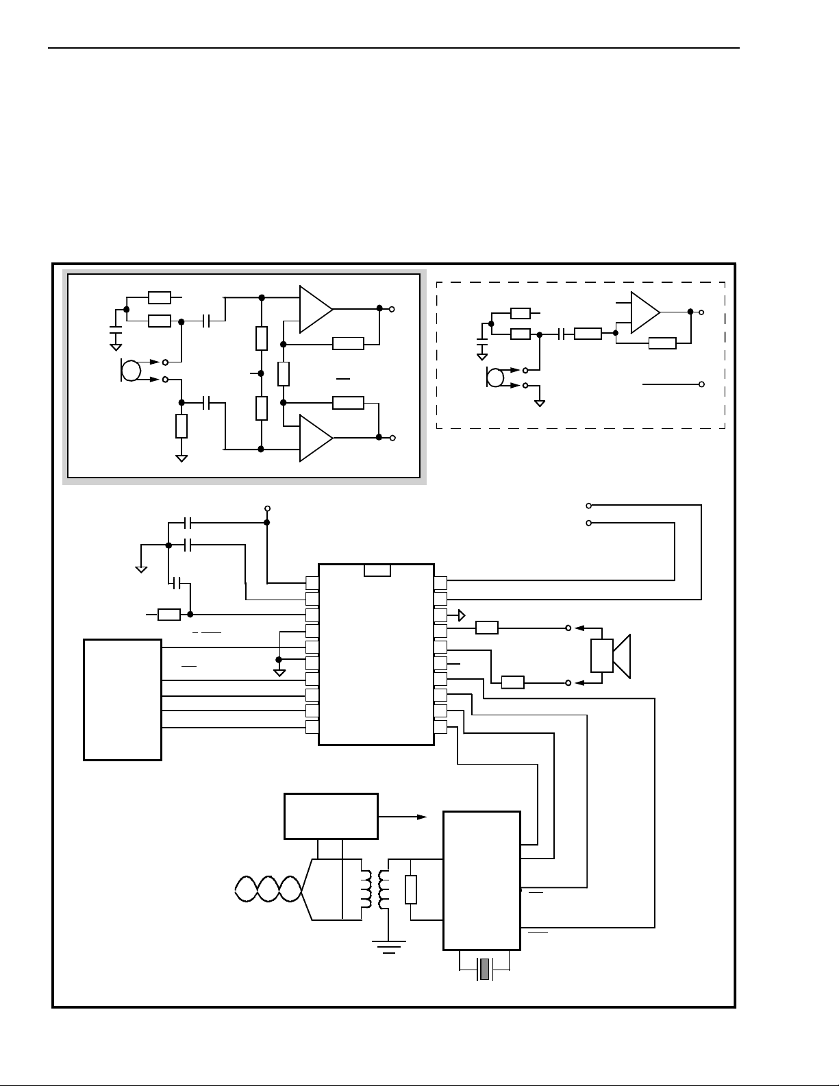
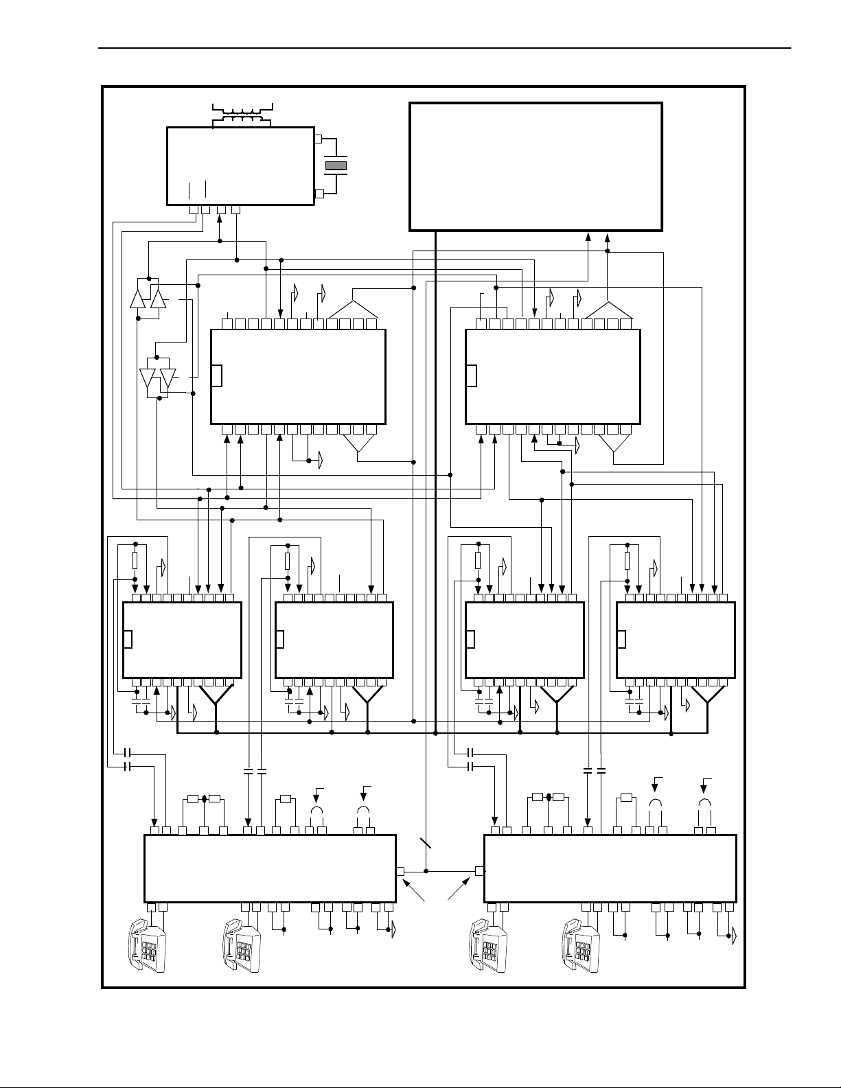
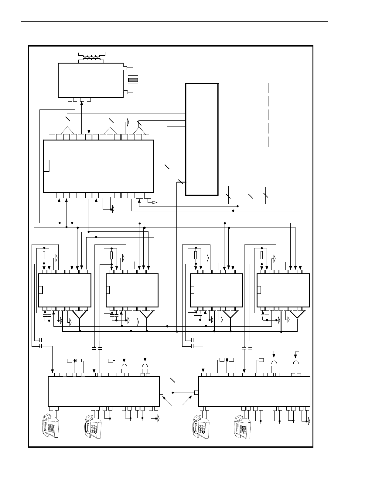
Figure 9 shows an application in a digital phone set.
Various configurations of pair gain drops are
depicted in Figures 10a and 10b using the MT9125
and MT9126, respectively.
330Ω
10 µF
511Ω
+5V
0.1 µF
100K
+
+
R
M+
10 µF
330Ω
+
+5V
1K
0.1 µF
VBias
T
+
-
R
M+
Electret
Microphone
INTEL
MCS-51
or
MOTOROLA
SPI
Micro-
Controller
+
+5V
511Ω
0.1 µF
0.1 µF
VBias
0.1 µF
100K
Differenti al Amplifi er
VBias
A/µ/IRQ
CS
SCLK
DATA1
DATA2
DATA2 Motorola
Mode only
Av = 1 + 2R
T
+
+5V
+
Single-ended Amplifier
75Ω
75Ω
20
19
18
17
16
15
14
13
12
11
Electret
Microphone
T
R
M-
Typical External Gain
()
1
2
3
4
MT9160
5
6
7
8
9
10
AV= 5-10
M+
M-
VBias
M-
150Ω
7-92
Twisted Pair
DC to DC
Converter
+5V
Lin
Z
Lout
T
MT8972
DNIC
10.24 MHz
Figure 9 - Digital Telephone Set
DSTi
DSTo
F0i
C4b
Page 17
Preliminary Information MT9160
74HCT124
or
17
15
16
101112
10.24 MHz
14
13
Serial Micro-port
Intel MCS-5 1
Motorola SPI
Nat Semi Microwire
24232221201918
5V
Static Control:
SLIC Functions
Optional QADPCM
functional control
14
15
16
17
MicroController
MT9125
123456789
101112 13
MT8972
MT8910
5V
74HCT124
C4b
DSTi
F0b
DSTo
5V
24232221201918
74HCT124
74HCT124
123456789
MT9125
5V
13
14
15
16
201918
17
1
MT9160
123456789
11
13
18
19
1
2
12
20
11
10
123456789
28
30
21
14
27
39
40
5V
201918
7
22
MH88622 Pair Gain SLIC 1
16
17
34
25
16
meter signal
-5V
MT9160
5V
15
I/P
5V
17
16
3
14
13
12
11
201918
2
12
13
14
15
201918
MT9160
28
123456789
30
21
22
10
120VDC ring
voltage
4
37
16
123456789
11
13
18
19
10 11
20
5V
17
Figure 10a - Pair Gain System
11
12
13
14
15
16
4
MT9160
10
meter signal
I/P
120VDC ring
voltage
34
4
37
7
MH88622 Pair Gain SLIC 2
3
38
-24VDC
15
26
1
2
Pins
5,8,9,17,23,32,33,36
39
40
14
27
5V
3
252616
38
15
-5V
-24VDC
7-93
Page 18
MT9160 Preliminary Information
C4b
F0b
3
282726
12345
25
or
MT8972
DSTi
DSTo
MT8910
3
5V
24232221201918
MT9126
678
9
1011121314
17
10.24 MHz
MicroController
3
Static Control:
SLIC Functions
Optional QADPCM
16
15
functional control
, RC1/2 - 8 x 2 SLIC’s
Reset
1
8
Serial Micro-port
Intel MCS-5 1
Motorola SPI
Nat Semi Microwire
16
3
16 control/status lines are:
9 control lines for QADPCM, some optional
LR1/2, ESE1/2, SHK1/2
, CS1, CS2, CS3, CS4
8
D-Channel access th rough Codec1 Microport as well as
8 signals for microport are:
Data1, Data2, SCKL, IRQ
C-Channel control of MT8910/MT8972
5V
13
14
15
201918
123456789
16
17
1
MT9160
11
13
18
19
1
2
12
20
10
11
201918
123456789
28
30
21
14
27
39
40
5V
5V
11
12
13
14
15
16
17
2
MT9160
10
120VDC ring
4
38
-24VDC
37
15
26
voltage
16
Pins
5,8,9,17,23,32,33,36
meter signal
I/P
7
34
22
MH88622 Pair Gain SLIC 1MH88622 Pair Gain SLIC 2
3
25
16
-5V
5V
13
14
15
201918
123456789
16
17
3
MT9160
11
13
18
19
1
2
12
20
10 11
28
39
201918
123456789
30
21
22
14
27
40
5V
5V
11
12
13
14
15
16
17
4
MT9160
meter signal
I/P
34
4
3
252616
38
-5V
-24VDC
7
37
120VDC ring
15
Figure 10b - Pair Gain System
10
voltage
7-94
Page 19
Preliminary Information MT9160
Absolute Maximum Ratings
Parameter Symbol Min Max Units
1 Supply Voltage V
2 Voltage on any I/O pin V
3 Current on any I/O pin (transducers excluded) I
4 Storage Temperature T
5 Power Dissipation (package) P
DD
- V
I/VO
I/IO
S
D
Recommended Operating Conditions - Voltages are with respect to V
Characteristi cs Sym Min Typ Max Units Test Conditions
1 Supply Voltage V
2 TTL Input Voltage (high)* V
3 TTL Input Voltage (low)* V
4 CMO S Input Voltage (high) V
5 CMO S Input Voltage (low) V
6 Operat ing Temperature T
* Excluding PWRST
which is a Schmitt Trigger Input.
DD
IHT
IHC
ILC
4.75 5 5.25 V
2.4 V
ILT
V
SS
4.5 V
V
SS
- 40 + 85 °C
A
DD
0.4 V Includes Noise margin =
DD
0.5 V
SS
- 0.3 7 V
VSS - 0.3 VDD + 0.3 V
± 20 mA
- 65 + 150 °C
750 mW
unless otherwise stated
SS
V Includes Noise margin =
400 mV
400 mV
V
Power Characteristics
Characteristi cs Sym Min Typ Max Units Test Conditions
1 Static Supply Current (clock
disabled, all fu nctio ns off, PDFDI /
PDDR=1, PWRS T= 0)
2 Dyna mic Supply Current :
Total all functions enabled I
Note 1: P owe r d el iv ere d to th e load is in additi on to th e bi as c urr e nt r e qu ire me nt s.
Note 2: I
is not a dd iti ve to I
DDFT
DDC1
.
I
DDC1
DDFT
350 µA Outputs unloaded, Inp ut
8.0 mA See Note 1 and 2.
signals static, not load ed
7-95
Page 20
MT9160 Preliminary Information
DC Electrical Characteristics
Characteristics Sym Min Typ
1 Input HIGH Voltage TTL inputs V
2 Input LOW Voltage TTL inputs V
3 Input HIGH Voltage CMOS inputs V
4 Input LOW Voltage CMOS inputs V
5 VBias Voltage Output V
6V
7 Input Leakage Current I
8 Positive Going Threshold
9 Output HIGH Current I
10 Output LOW Current I
11 Output Leakage Current I
12 O utput Capacitan ce C
13 Input Capacita nce C
† DC Electrical Characteristics are over recommended temperature range & recommended power supply voltages.
‡ Typical figures are at 25 °C and are for desig n aid only: not guaranteed and not subject to produ ctio n testin g.
Output Voltage V
Ref
Voltage (PWRST
only)
Negative Going Threshold
Voltage (PWRST
only)
†
- Voltages are with respect to ground (V
IHT
IHC
ILC
Bias
Ref
V
V
OH
OL
OZ
ILT
IZ
T+
2.0 V
3.5 V
VDD/2 V Max. Load = 10kΩ
V
/2-1.5
DD
0.1 10 µA VIN=VDD to V
3.7
T-
- 5 - 16 mA VOH = 2.4V
510 mAV
0.01 10 µA V
o
i
15 pF
10 pF
) unless otherwise stated.
SS
‡
Max Units Test Conditions
0.8 V
1.5 V
V No load
V
1.3
V
= 0.4V
OL
= VDD and V
OUT
SS
SS
Clockin Tolerance Characteristics (ST-BUS Mode)
Characteristics Min Typ
1C4i
† AC Electrical Characteristics are over recommended temperature range & recommended power supply voltages.
‡ Typical figures are at 25 °C and are for desig n aid only: not guaranteed and not subject to produ ctio n testin g.
Freq u en cy 4095.6 4096 4 0 96. 4 kHz (i.e., 100 ppm)
‡
Max Units Test Conditions
7-96
Page 21
Preliminary Information MT9160
AC Characteristics† for A/D (Transmit) Path - 0dBm0 = 1.421V
A-Law, at the Codec. (V
Characteristics Sym Min Typ
1 Analog input equivalent to
overload decision
2 Absolute half-channel gain
M ± to Dou t G
Tolerance at all other transmit
filter set tin g s
(1 to 7dB)
3 Gain tracking vs. input level
CCITT G.714 Method 2
4 Signal to total Distortion vs. input
level.
CCITT G.714 Method 2
5 Transmit Idle Channel Noise N
6 Gain relative to gain at 1020Hz
<50Hz
60Hz
200Hz
300 - 3000 Hz
3000 - 3400 Hz
4000 Hz
>4600 Hz
=1.0 volts and V
Ref
=2.5 volts.)
Bias
A
A
G
G
D
N
G
Li3.17
Li3.14
AX1
AX2
TX
QX
CX
PX
RX
-0.3
-0.6
-1.6
35
29
24
-0.25
-0.9
‡
Max Units Test Conditions
5.79
6.0
6.0
15.3
±0.2 dB
0.3
0.6
1.6
15
-71
16
-69
-25
-30
0.0
0.25
0.25
-12.5
-25
for µ-Law and 1.477V
rms
Vp-p
Vp-p
dB
dB
dB
dB
dB
dB
dB
dB
dBrnC0
dBm0p
dB
dB
dB
dB
dB
dB
dB
for
rms
µ-Law
A-Law
Both at Codec
Transmit filter gain=0dB
setting.
TxINC = 0*
TxINC = 1*
@1020 Hz
3 to -40 dBm0
-40 to -50 dBm0
-50 to -55 dBm0
0 to -30 dBm0
-40 dBm0
-45 dBm0
µ-Law
A-Law
7 Absolute Delay D
AX
360 µs at frequency of minimum
delay
8 Group Delay relative to D
AX
9 Power Supply Rejection
f=1020 Hz
f=0.3 to 3 kHz
f=3 to 4 kHz
f=4 to 50 kHz
† AC Electrical Characteristics are over recommended temperature range & recommended power supply voltages.
‡ Typical figures are at 25 °C and are for desig n aid only: not guaranteed and not subject to produ ctio n testing.
* Note: TxINC, refer to Control Register 1, address 00h.
D
DX
PSSR
PSSR1
PSSR2
PSSR3
750
380
130
750
37
40
35
40
µs
µs
µs
µs
dB
dB
dB
dB
500-600 Hz
600 - 1000 Hz
1000 - 2600 Hz
2600 - 2800 Hz
±100mV peak signal on
V
DD
µ-law
PSSR1-3 not production
tested
7-97
Page 22
MT9160 Preliminary Information
AC Characteristics† for D/A (Receive) Path - 0dBm0 = 1.421V
(V
=1.0 volts and V
Ref
Characteristics Sym Min Typ
1 Analog output at the Codec full
scale
2 Absolute half-channel gain.
Din to HSPKR±
Tolerance at all other receive
filter settings
(-1 to -7dB)
3 Gain tracking vs. input level
CCITT G.714 Method 2
4 Signal to total distortion vs. input
level.
CCITT G.714 Method 2
5 Receive Idle Channel Noise N
6 Gain relative to gain at 1020Hz
200Hz
300 - 3000 Hz
3000 - 3400 Hz
4000 Hz
>4600 Hz
=2.5 volts.)
Bias
A
Lo3.17
A
Lo3.14
G
G
G
G
G
G
N
G
AR1
AR2
AR3
AR4
TR
QR
CR
PR
RR
-0.3
-0.6
-1.6
35
29
24
-0.25
-0.90
‡
Max Units Test Conditions
5.704
5.906
0
-6
-6
-12
±0.2 dB
13
15.5
-78.5
0.25
0.25
0.25
-12.5
for µ-Law and 1.477V
rms
Vp-p
Vp-p
dB
dB
dB
dB
0.3
0.6
1.6
dB
dB
dB
dB
dB
dB
dBrnC0
-77
dBm0p
dB
dB
dB
dB
-25
dB
for A-Law, at the Codec.
rms
µ-Law
A-Law
DrGain=0, RxINC =1*
DrGain=0, RxINC =0*
DrGain=1, RxINC =1*
DrGain=1, RxINC =0*
@ 1020 Hz
3 to -40 dBm0
-40 to -50 dBm0
-50 to -55 dBm0
0 to -30 dBm0
-40 dBm0
-45 dBm0
µ-Law
A-Law
7 Absolute Delay D
8 Group Delay relative to D
AR
9 Crosstalk D/A to A/D
A/D to D/A
† AC Electrical Characteristics are over recommended temperature range & recommended power supply voltages.
‡ Typical figures are at 25 °C and are for desig n aid only: not guaranteed and not subject to produ ctio n testin g.
* Note: RxINC, refer to Contro l Register 1, addre s s 00h.
D
CT
CT
AR
DR
RT
TR
240 µs at frequency of min. delay
750
380
130
750
-74
-80
µs
µs
µs
µs
dB
dB
500-600 Hz
600 - 1000 Hz
1000 - 2600 Hz
2600 - 2800 Hz
G.714.16
CCITT
7-98
Page 23
Preliminary Information MT9160
AC Electrical Characteristics† for Side-tone Path
Characteristics Sym Min Typ
‡
Max Units Test Conditions
1 Absolute path gain
gain adjust = 0dB
G
AS1
G
AS2
-16.63
-10.63
dBdBRxINC = 0*
RxINC = 1*
M± input s to HSPKR± outp uts
1000 Hz at STG2 =1
† AC Electrical Characteristics are over recommended temperature range & recommended power supply voltages.
‡ Typical figures are at 25 °C and are for desig n aid only: not guaranteed and not subject to produ ctio n testing.
* Note: RxINC, refer to Control Register 1, address 00h.
Electrical Characteristics† for Analog Outputs
Characteristics Sym Min Typ‡Max Units Test Conditions
1 EarpI ece load im pedance E
2 Allowable earpiece capacitive
E
load
3 Earpiece harmonic distortion E
† El ectri ca l Characte risti cs are over recom m ende d tempera tu re range & recommen ded power supply voltage s.
‡ Typical figures are at 25 °C and are for desig n aid only: not guaranteed and not subject to produ ctio n testing.
* Note: RxINC, refer to Control Register 1, address 00h.
260 300 ohms across HS PKR±
ZL
CL
D
300 pF each pin: HSPKR+,
0.5 % 300 ohms load across
HSPKR± (tol-15%),
VO≤693mV
Rx gain=0dB
HSPKR-
, RxINC=1*,
RMS
Electrical Characteristics† for Analog Inputs
2.90
1.03
‡
Max Units Test Conditions
Vp-p
Vp-p
TxINC = 0, A/µ = 0 *
TxINC = 1, A/µ = 1 *
Tx filter gain=0dB setting
Characteristics Sym Min Typ
1 I nput voltage with out overloa ding
Codec
across M+/M- V
2 I nput Impeda n ce Z
† El ectri ca l Characte risti cs are over recom m ende d tempera tu re range & recommen ded power supply voltage s.
‡ Typical figures are at 25 °C and are for desig n aid only: not guaranteed and not subject to produ ctio n testing.
* Note: TxINC, refer to Control Register 1, address 00h.
IOLH
I
50 kΩ M+/M- to V
SS
7-99
Page 24
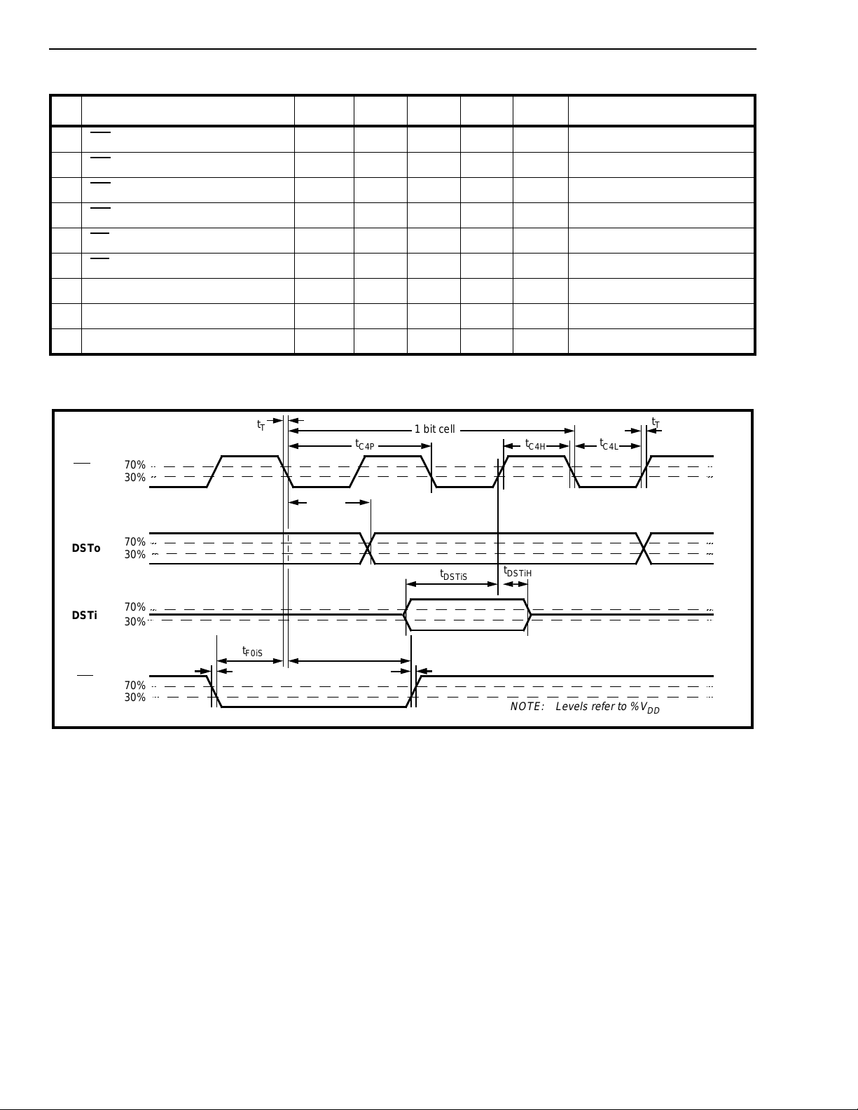
MT9160 Preliminary Information
AC Electrical Characteristics† - ST-BUS Timing (See Figure 11)
Characteristi cs Sym Min Typ
‡
Max Un its Test Conditio ns
1C4i
2C4i
3C4i
4C4i
5F0i
6F0i
7 DSTo Delay t
8 DSTi Setup Time t
9 DSTi Hold Time t
† Timing is over recommended temperature range & recommended power supply voltages.
‡ Typical figures are at 25 °C and are for desig n aid only: not guaranteed and not subject to produ ctio n testin g.
* Note : All co nd it ions → data-da ta, data -HiZ , HiZ-data.
Clock Period t
Clock High period t
Clock Low period t
Clock Transition Time t
Frame Pulse Setup Time t
Frame Pulse Hold Time t
C4i
DSTo
70%
30%
70%
30%
C4P
C4H
C4L
T
F0iS
F0iH
DSToD
DSTiS
DSTiH
T
t
DSToD
50 ns
50 ns
30 ns
30 ns
t
C4P
244 ns
122 ns
122 ns
20 ns
100 125 ns CL = 50pF, 1kΩ load.*
1 bit cell
t
C4H
t
t
DSTiS
DSTiH
t
C4L
t
Tt
DSTi
F0i
70%
30%
70%
30%
t
t
F0iS
T
t
F0iH
t
T
NOTE: Levels refer to %V
DD
Figure 11 - ST-BUS Timing Diagram
7-100
Page 25
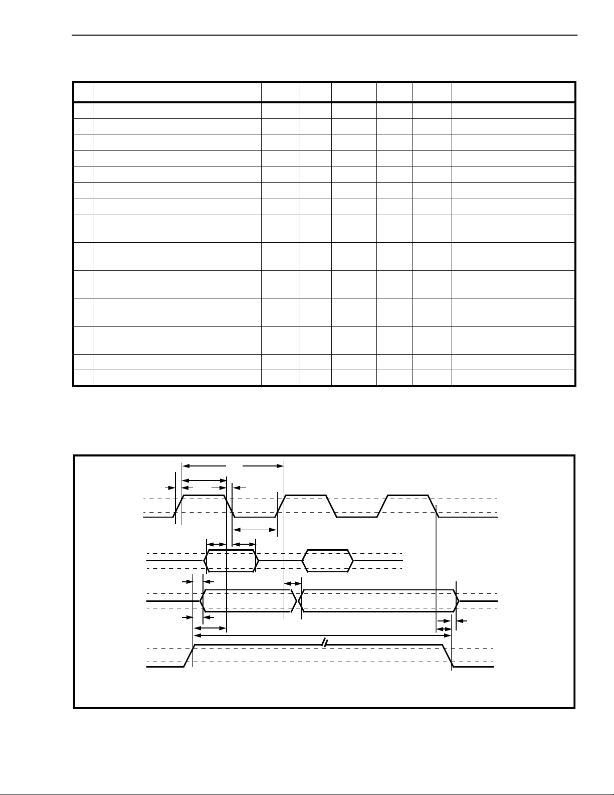
Preliminary Information MT9160
AC Electrical Characteristics† - SSI BUS Synchronous Timing (see Figure 12)
Characteristics Sym Min Typ
‡
Max Units Test Conditions
1 BCL Clock Perio d t
2 BCL Pulse W idth High t
3 BCL Pulse W idth Low t
4 BCL Rise/ Fall Time t
5 Strobe Pulse Width t
6 St robe setup ti me before BCL fall ing t
7 St robe hold ti me af ter B CL fall ing t
8 Dou t High Impedance to Active Low
BCL
BCLH
BCLL
R/tF
ENW
SSS
SSH
t
DOZL
244 19 53 ns BCL=4096 kHz to 512 kHz
122 ns BCL=4096 kHz
122 ns BCL=4096 kHz
20 ns Note 1
80
80
8 x t
BCL
t
BCL
t
BCL
-80
-80
ns Note 1
ns
ns
90 ns CL=150 pF, RL=1K
from Strobe rising
9 Dout High Impedance to Active High
t
DOZH
90 ns CL=150 pF, RL=1K
from Strobe rising
10 Dout Active Low to High Impedance
t
DOLZ
90 ns CL=150 pF, RL=1K
from Strobe falling
11 Dout Active High to High Impedance
t
DOHZ
90 ns CL=150 pF, RL=1K
from Strobe falling
12 Dout Delay (high and low) from BCL
t
DD
90 ns CL=150 pF, RL=1K
rising
13 Din Setup time before BCL f alli ng t
14 Din Hold Time from BCL falling t
† Timing is over recommended temperature range & recommended power supply voltages.
‡ Typical figures are at 25°C and are for design aid only: not guaranteed and not subject to producti on testing.
NOTE 1: Not production tested, guaranteed by design.
DIS
DIH
50 ns
50 ns
CLOCKin
(BCL)
Din
Dout
STB
70%
30%
70%
30%
70%
30%
70%
30%
t
R
t
t
DOZL
DOZH
t
t
BCLH
BCL
t
F
t
BCLL
t
t
DIS
DIH
t
DD
t
SSS
t
ENW
NOTE: Levels refer to % VDD (CMOS I/O)
Figure 12 - SSI Synchronous Timing Diagram
t
SSH
t
DOLZ
t
DOHZ
7-101
Page 26
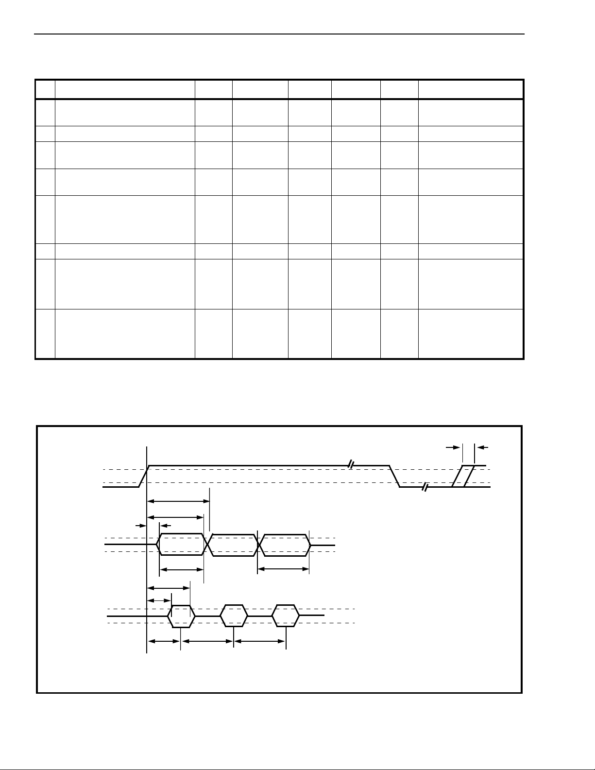
MT9160 Preliminary Information
AC Electrical Characteristics† - SSI BUS Asynchronous Timing (note 1) (see Figure 13)
Characteristi cs Sym Min Typ
‡
Max Units Test Conditions
1 Bit Cell Period T
DATA
7812
nsnsBCL=128 k Hz
3906
2 Frame Jitt er T
3 Bit 1 Dout Delay from STB
t
dda1
j
600 ns
Tj+600 ns CL=150 pF, RL=1K
going high
4 Bit 2 Dout Delay from STB
going high
5 Bit n Dout Delay from STB
going high
6 B it 1 Da t a Bou n d a ry T
7 Din Bit n Data Setup time f rom
STB rising
t
dda2
t
ddan
DATA1
t
SU
600+
T
DATA-Tj
600 +
(n-1) x
T
DATA-Tj
T
DATA-Tj
T
\2
DATA
+500ns-T
j
600+
T
DATA
600 +
(n-1) x
T
DATA
600 +
T
DATA+Tj
600 +
(n-1) x
T
DATA+Tj
T
DATA+Tj
ns CL=150 pF, RL=1K
ns CL=150 pF, RL=1K
ns
ns n=1-8
+(n-1) x
T
DATA
T
8 Din Data Hold tim e from STB
rising
t
ho
+500ns+T
DATA
\2
j
ns
+(n-1) x
T
DATA
† Timing is over recommended temperature range & recommended power supply voltages.
‡ Typical figures are at 25°C and are for design aid only: not guaranteed and not subject to producti on testing.
NOTE 1: Not production tested, guaranteed by design.
BCL=256 k Hz
n=3 to 8
STB
Dout
Din
70%
30%
70%
30%
70%
30%
t
dda1
t
dda2
t
dha1
Bit 1 Bit 2 Bit 3
T
t
su
DATA
T
DATA1
t
ho
D1
/2
T
D2
DATA
T
DATA
T
DATA
D3
NOTE: Levels refer to % VDD (CMOS I/O)
Figure 13 - SSI Asynchronous Timing Diagram
T
j
7-102
Page 27
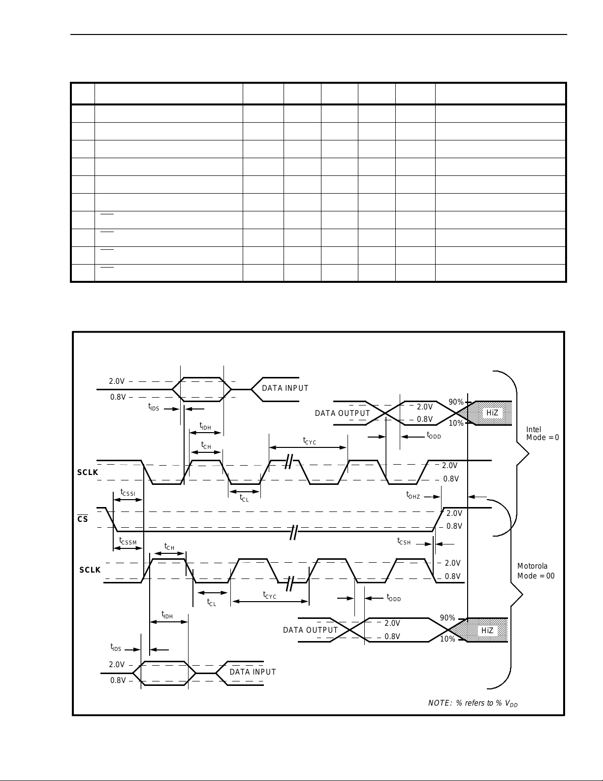
Preliminary Information MT9160
AAAA
AAAA
AAAA
AAAA
AAAA
AAAA
AAAA
AAAA
AAAA
AAAA
AAAA
AAAA
AAAA
AAAA
AAAA
AAAA
AAAA
AAAA
AAAA
AAAA
AAAA
AAAA
AAAA
AAAA
AAAA
AAAA
AAAA
AAAA
AAAA
AAAA
AAAA
AAAA
AAAA
AAAA
AAAA
AAAA
AAAA
AAAA
AAAA
A
A
A
A
A
A
AC Electrical Characteristics† - Microport Timing (see Figure 14)
Characteristics S y m Min Typ
‡
Max Units Test Conditions
1 Inpu t data setup t
2 Inpu t data hold t
3 Output data delay t
4 Serial clock period t
5 SCL K pulse width high t
6 SCL K pulse width low t
7CS
8CS
9CS
10 CS
setup-Intel t
setup-Motorola t
hold t
to output high impedance t
IDS
IDH
ODD
CYC
CH
CL
CSSI
CSSM
CSH
OHZ
100 ns
30 ns
100 ns CL = 150pF, RL = 1K *
500 1000 ns
250 500 ns
250 500 ns
200 ns
100 ns
100 ns
100 ns CL = 150pF, RL = 1K
† Timing is over recommended temperature range & recommended power supply voltages.
‡ Typical figures are at 25°C and are for design aid only: not guaranteed and not subject to producti on testing.
* Note : All co nd it ions → data-data, data-HiZ, HiZ-data.
2.0V
0.8V
t
IDS
t
IDH
t
CH
DATA INPUT
DATA OUTPUT
t
CYC
2.0V
0.8V
t
90%
10%
ODD
HiZ
Intel
Mode = 0
SCLK
CS
SCLK
t
IDS
2.0V
0.8V
t
CSSI
t
CSSM
2.0V
0.8V
t
t
CL
OHZ
2.0V
0.8V
t
t
ODD
2.0V
0.8V
CSH
2.0V
0.8V
90%
10%
Motorola
Mode = 00
HiZ
t
CH
t
t
CL
t
IDH
CYC
DATA OUTPUT
DATA INPUT
NOTE: % refers to % V
DD
Figur e 14 - Mic ro por t Tim i ng
7-103
Page 28

MT9160 Preliminary Information
Notes:
7-104
 Loading...