

Page 1
CMOS
MT9080B
SMX - Switch Matrix Module
Features
• 16 bit wide data bus I/O
• 16 bit address bus
• Microprocessor Interface
• 2048 x 16 bit wide memory SRAM
• Interfaces with Mitel’s MT9085B to form larger
switch mitoses
• Variable clock and frame rates
Applications
• Small and medium digital switch matrices
• Telephony equipment - PBX, CO equipment,
digital cross connect, digital local loop
• Datacom equipment - access concentrators,
Lan/Wan gateways
DS5140 ISSUE 4 March 1999
Ordering Information
MT9080BP 84 Pin PLCC
-40°C to 70°C
Description
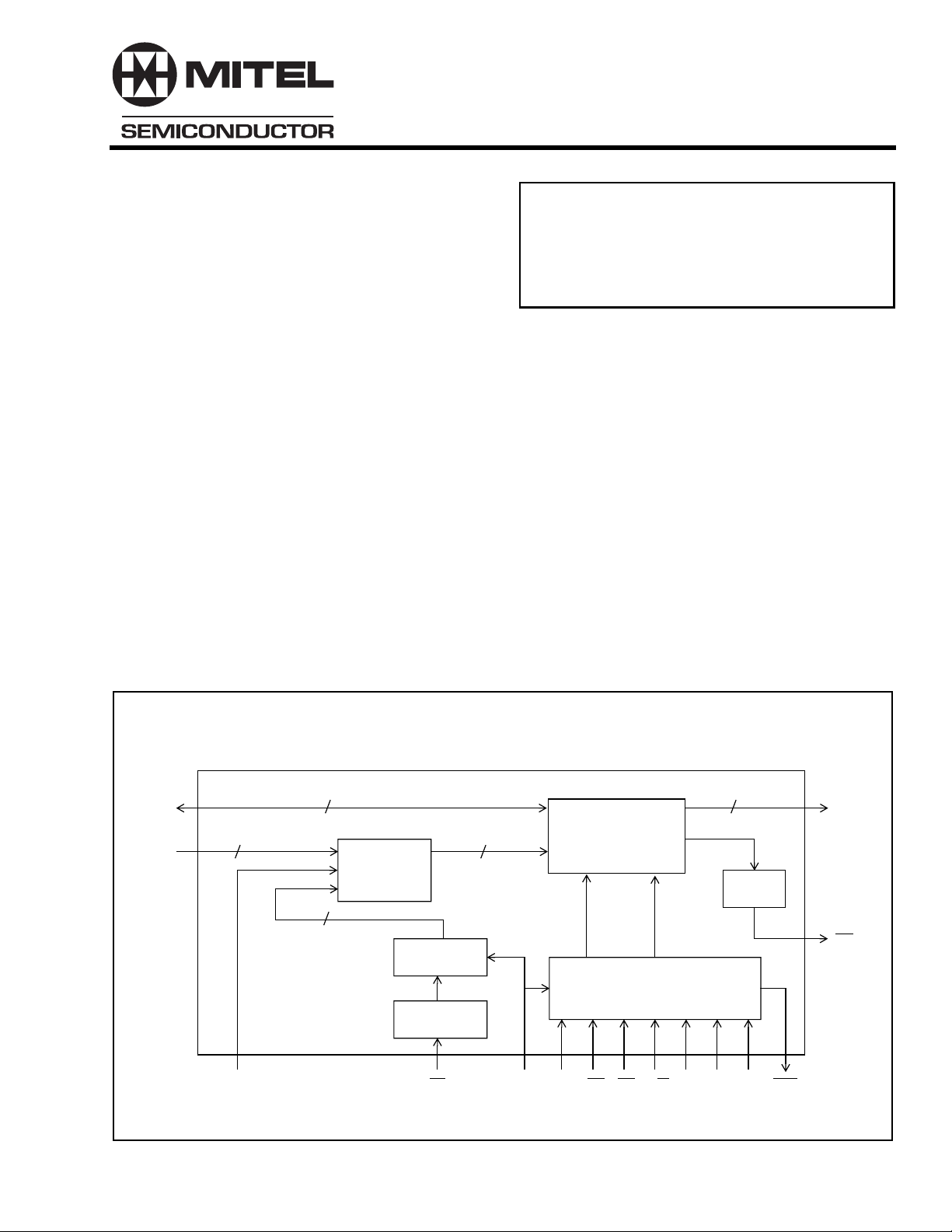
The MT9080B is a flexible memory module suitable
for use as a basic building block in the construction
of customized digital switching matrices. It can be
configured as either a Data Memory or a Connection
Memory, and is designed to interface with Mitel’s
MT9085B. Interface to the device is via 16 bit wide
data and address busses. The MT9080B can
operate with variable clock rates up to 16.7 MHz.
D0i/D15i
A0-A15
ME
16
16
16
Address
MUX
11
11 Bit
Counter
Counter
Reset
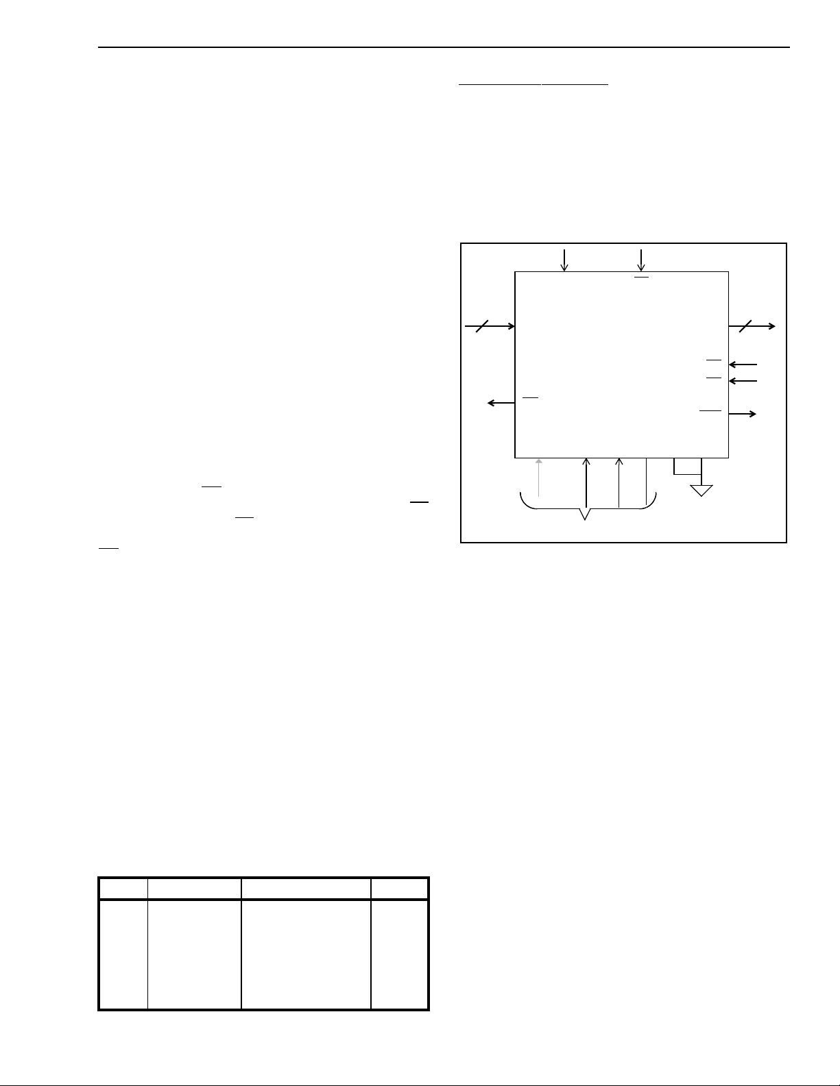
FP CK ODE DS CS R/WMxMyMzDTA
Figure 1 - Functional Block Diagram
2048 x 16
Static
Memory
WR
ENABLE
Control Interface
PRECHARGE
16
CRC
D0o/
D15o
CD
2-101
Page 2
MT9080B CMOS
D8i
D9i
D10i
D11i
VSS
D12i
D13i
D14i
D15i
VSS
CK
VDD
VSS
IC
IC
FP
CS
DS
R/W
DTA
NC
VSS
D7i
D6i
D5i
D4i
VSS
D3i
D2i
D1i
VSS
VDD
D15o
D14o
D13o
D12o
VSS
D11o
D10o
D9o
D0i
8
6
4
12
10
14
16
18
20
22
24
26
28
30
32
34
36
38
MxMyMz
NC
ME
VSS
ODE
2
84
84 PIN PLCC
40
NC
44
42
IC
IC
NC
VSS
VDD
82
80
46
48
A0A1A2A3A4A5A6
D8o
78
50
VSS
76
74
D7o
D6o
72
D5o
D4o
70
VSS
D3o
68
D2o
D1o
66
D0o
VSS
64
VDD
62
CD
A15
60
A14
A13
58
A12
A11
56
A10
A9
A8
54
52
A7
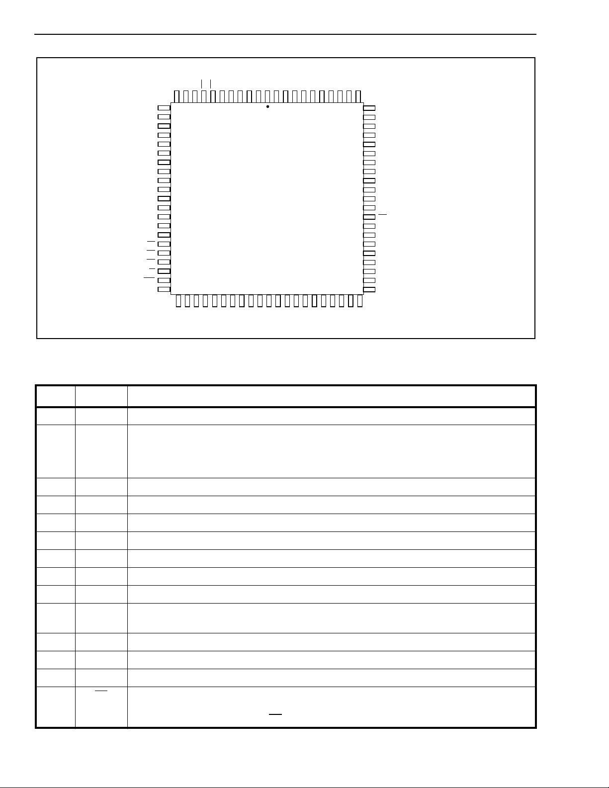
Figure 2 - Pin Connections
Pin Description
Pin # Name Description
1VSSGround.
2-5 D0i-D3i Input/Microport Data Bus. This is part of a 16 bit data bus. The data bus is bidirectional in
Connect Memory mode where it is typically interfaced to a microprocessor. In all other
modes the data bus is an input. Data to be switched through the device is clocked in at this
port.
6VSSGround.
7-10 D4i-D7i Input/Microport Data Bus. See description for pins 2-5 above.
11 V
SS
12-15 D8i-D11i Input/Microport Data Bus. See description for pins 2-5 above.
16 V
SS
17-20 D12i-D15i Input/Microport Data Bus. See description for pins 2-5 above.
21 V
SS
22 CK Clock. Master clock input which is used to clock data into and out of the de vice. It also cloc ks
Ground.
Ground.
Ground.
the internal 11 bit counter.
23 V
24 V
DD
SS
+5V supply input.
Ground.
25,26 IC Internal Connection. Should be tied to VSS for normal operation.
27 FP Frame Pulse. An active low signal that serves as a synchronous clear for the internal 11 bit
counter in all modes except Shift Register mode. The counter is cleared on a rising edge of
CK. In the Shift Register mode, FP serves to align channel boundaries.
2-102
Page 3
CMOS MT9080B
Pin Description
Pin # Name Description
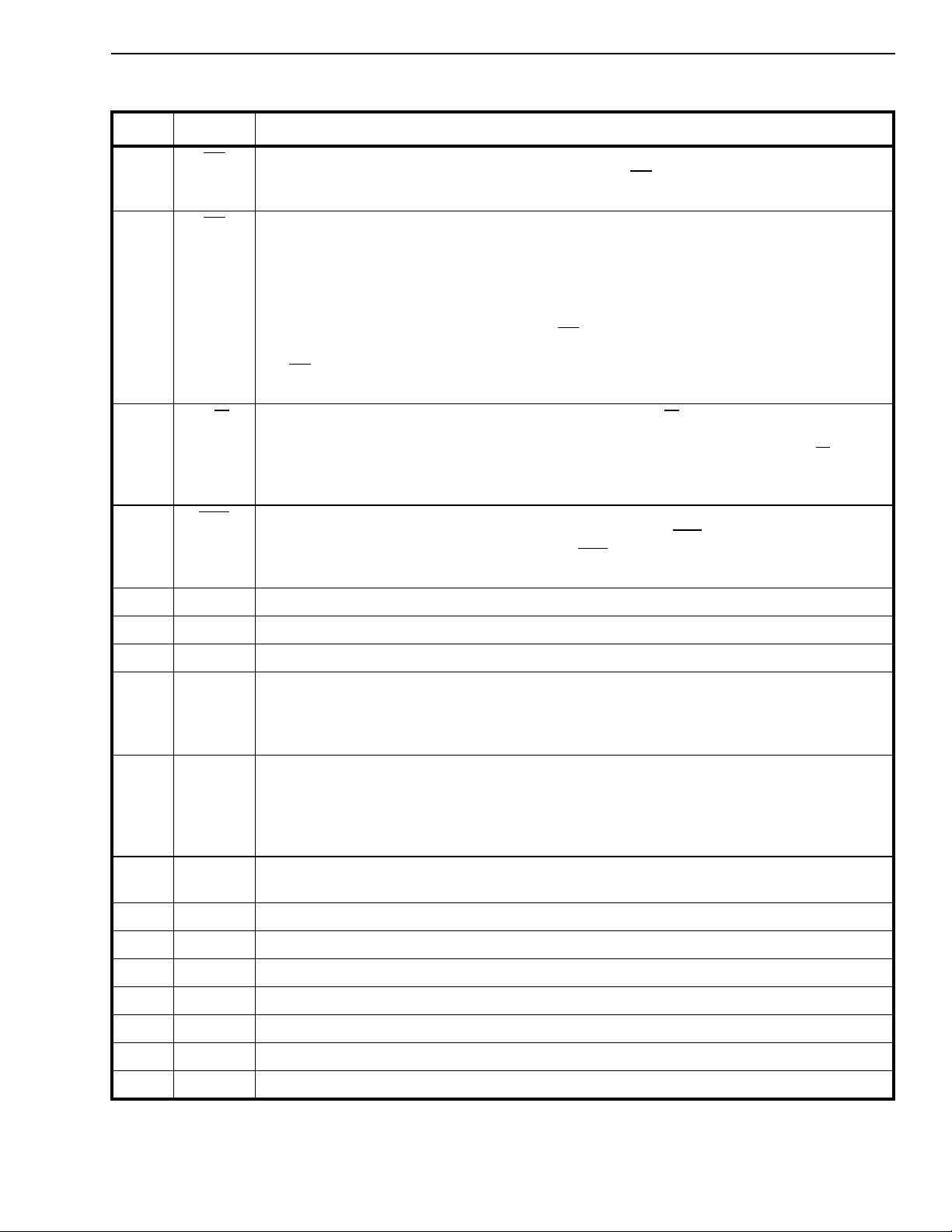
28 CS Chip Select. Active Low input. Selects the device for microport access in connect memory,
data memory, external and shift register modes. Tying CS high will disable output data
drivers (D0-D15o) in all modes except connect memory and shift register modes.
29 DS Data Strobe. Active low input. Indicates to the SMX that valid data is present on the
microport data bus during a write operation or that the SMX must output data on a read
operation.
In Connect Memory modes, a low level applied to this input during a write operation indicates
to the SMX that valid data is present on the microport data bus. During a read operation the
low going signal indicates to the SMX that it must output data on the microport data bus.
In Data Memory and External modes, when DS is high, the output data bus D0o-D15o will be
disabled. The input data bus D0i-D15i is not affected.
The DS input has no effect on the input and output busses in Counter or Shift Register
modes.
30 R/W Read/Write Enable. Data is written into the device when R/W is low and read from it when it
is high. This control input is disabled in data memory and shift register modes. It should be
tied to VSS or VDD in these modes. In counter and external modes, the state of R/W pin is
clocked in with the rising edge of CK. The actual read or write operation will be implemented
on the next rising clock edge.
31 DTA Data Transfer Acknowledge. Open drain output which is pulled low to acknowledge
completion of microport data transfer. On a read of the SMX,DT A low indicates that the SMX
has put valid data on the data bus. On a write, DTA low indicates that the SMX has
completed latching the data in.
32 NC No Connection.
33 V
SS
Ground.
34 NC No Connection.
35 ODE Output Data Enab le. Control input which enab les the output data bus. Pulling this input low
will place the data bus in a high impedance state. The level on this pin is latched by a rising
edge of CK. The output drivers will be enabled or disabled with the rising edge in the next
timeslot (see Fig. 24 for applicable timing in different modes).
36 ME Message Enable. When tied high the data latched in on the address bus is clocked out on
D0o-D15o. When ME is tied low, the contents of the addressed memory location will be
output on the bus. The level on this pin is latched in with the rising edge of the clock. The
actual mode change is implemented on the rising edge in the next timeslot. Refer to Figures
25 and 26 for more timing information.
37 Mx Mode X. One of three inputs which permit the selection of different operating modes for the
device. Refer to Table 1 for description of various modes.
38 My Mode Y. See description for pin 37.
39 Mz Mode Z. See description for pin 37.
40 NC No Connection.
41, 42 IC Internal Connection. Leave open for normal operation.
43 V
44 V
SS
DD
Ground.
Supply Voltage. +5V.
45 NC No Connection.
2-103
Page 4
MT9080B CMOS
Pin Description
Pin # Name Description
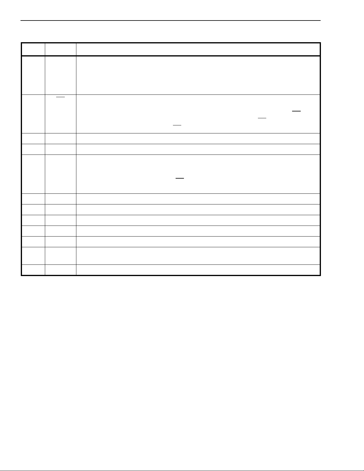
46-61 A0-A15 Address Bus. These inputs have three different functions. Inputs A0-A10 are used to
address internal memory locations during read or write operations in all modes except Shift
Register mode. In Shift Register mode, the levels latched in on A0-A10 program the delay
through the device. When the ME pin is tied high, the data latched in on A0-A15 is clocked
out on to the data bus (D0o-D15o).
62 CD Change Detect. Open drain output which is pulled low when a change in the memory
contents from one frame to the next is detected by a Cyclic Redundancy Check (CRC).
Changes in memory contents resulting from microprocessor access do not cause CD to go
low. The output is reset to its normal high impedance state when the DS input is strobed,
while the device has been selected (CS is low).
63 V
64 V
DD
SS
Supply Voltage. +5V.
Ground.
65-68 D0o-D3o Output Data Bus. These three state outputs are part of a 16 bit data bus which is used to
clock out data from the device. Data is clocked out with the rising edge of the clock. See
Figures 24 to 26 for timing information. The bus is activ ely driven when ODE is tied high. It is
disabled when ODE is tied low. Tying CS high will also disable the output data bus in all
modes except Connect Memory and Shift Register Modes.
69 V
SS
Ground.
70-73 D4o-D7o Output Data Bus. See description for pins 65-68.
74 V
SS
Ground.
75-78 D8o-D11o Output Data Bus. See description for pins 65-68.
79 V
SS
Ground.
80-83 D12o-D15oOutput Data Bus. See description for pins 65-68.
84 V
DD
Supply Voltage. +5V.
2-104
Page 5
CMOS MT9080B
Functional Description
The SMX is a flexible memory module suitable for
use in the construction of timeslot interchange
circuits used in PCM voice or data switches. The
device can be configured as a data memory or a
connection memory.
The SMX has separate 16 bit input and output data
busses. A 16 bit address bus and a full
microprocessor interface is also provided.
Data is clocked into and out of the device with the
signal applied at the CK (clock) input. Depending on
the mode of operation, the memory locations for the
read or write operation can be addressed
sequentially by the internal counter or randomly via
the external address bus. A messaging sub-mode,
which permits the data latched in on the address bus
to be multiplexed on to the output data bus, is also
available (see ME pin description).
The SMX ensures integrity of the stored data by
performing a Cyclic Redundancy Check (CRC) on a
per frame basis. When a change in the memory
contents is detected from one frame to the next, the
Change Detect (CD) pin is pulled low. The output will
be reset to its normal high impedance state when DS
input is strobed while CS is low (i.e., while the device
has been selected for microprocessor access). The
CD output is not pulled low when the memory
contents have been modified by a processor access
to the device.
Modes Of Operation
The SMX can be programmed to operate in one of
eight modes as summarized in Table 1. The different
modes are used to realize specific switch
implementations. For example, to implement a 1024
channel switch, two SMXs are required. One is
operated in Data Memory mode, while the second is
operated in Connect Memory mode. A 2048 channel
switch can be realized using three SMXs. Two of the
devices are operated, alternatively, in Counter and
External modes, the third serves as the Connection
Memory. A detailed description of the
implementation is presented in the Applications
section of this data sheet. An outline of the device
functionality in each mode is presented below.
Mode MXMYM
1
0
2
0
3
0
4
0
5
1
6
1
7
1
8
1
Z
0
0
0
1
1
0
0
1
1
Data Memory - 1
1
Data Memory - 2
0
Connect Memory - 1
1
Connect Memory - 2
0
Counter Mode
1
External Mode
0
Shift Register Mode
1
Data Memory - 3
Table 1. SMX Modes of Operation
Name Abbr.
DM-1
DM-2
CM-1
CM-2
CNT
EXT
SR
DM-3
Data Memory Mode-1
Data Memory Mode-1 is designed for use in the
construction of a 1024 Channel Switch Matrix. Data
on the D0-D15 input bus is clocked into the SMX and
stored in memory locations addressed by the internal
11 bit counter. Data is clocked out according to the
addresses asserted on the address bus. The pin
configuration of the device in this mode is illustrated
in Figure 3
Data
Input
16
CK
-D15
D0
i
i
CD
A0-A15 ME ODE ZYZ
From Control Interface
FP
MODE
D0
-D15
o
CS
DS
DTA
o
Data
Output
16
Figure 3 - Data Memory Modes 1 and 2 Pinout
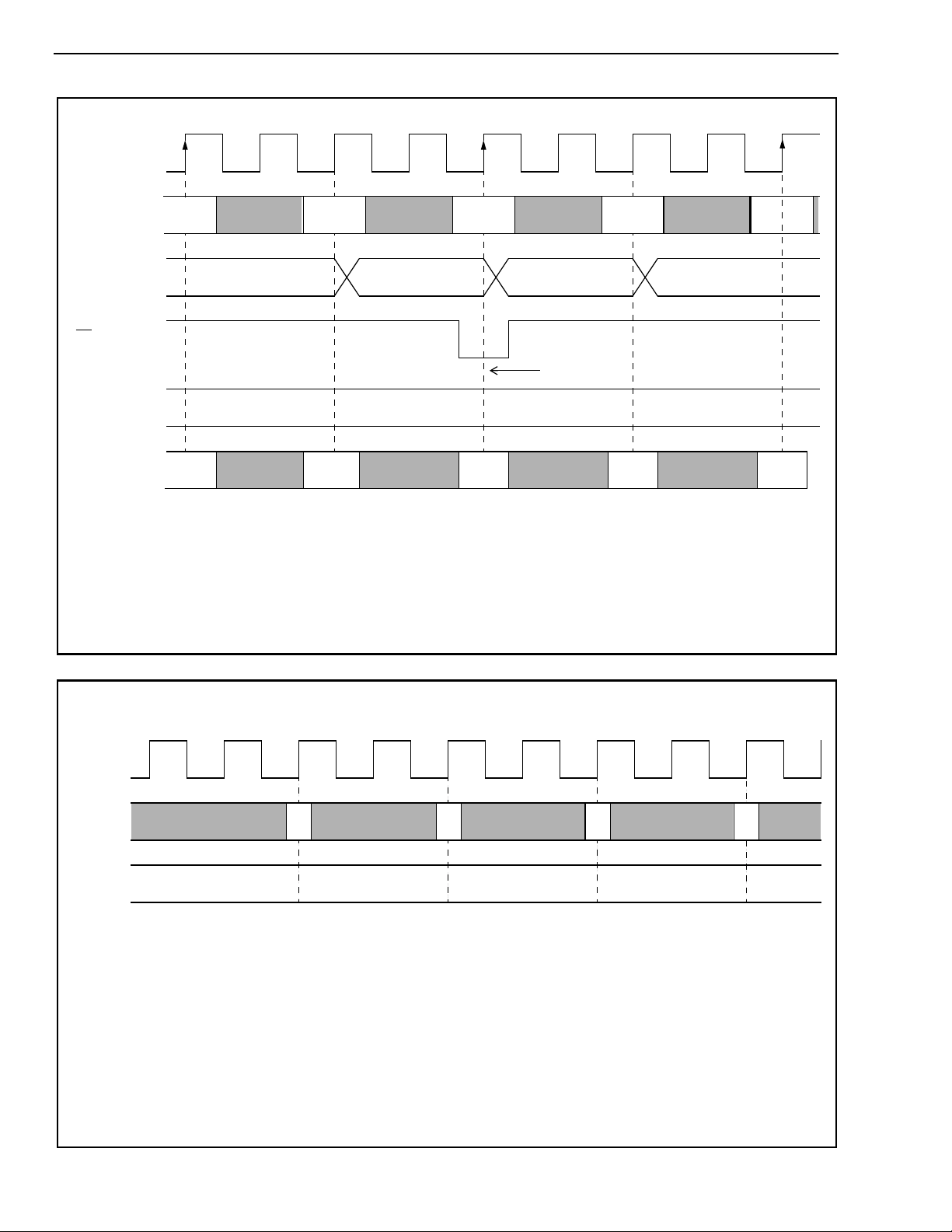
The timing for the read and write operation is
illustrated in Figure 4. The first half of each clock
period is used for precharging the internal bus. Data
is latched in and out of the device with rising edge of
the CK clock. Correct operation of the device in this
mode requires 2048 clock cycles in a single frame
defined by the frame pulse. Consequently, for
switching of 64 kbit/s PCM voice channels, the clock
frequency must be 16.384 Mbit/s with a frame rate of
8 kHz.
The address supplied on the address bus is latched
in with the first positive clock edge in a channel
timeslot. The contents of the memory location
addressed will be clocked out on D0-D15o with the
first positive clock edge in the next timeslot (see
Figure 4).
In Data Memory Mode-1, the delay through the
switch depends on the number of channel timeslots
between the input channel and the output channel. If
the time difference between the input channel and
output channel is less than two channels, data
clocked into the device in the current frame will be
clocked out in the next frame. If the difference is
greater than or equal to two channels, data will be
clocked out in the same frame. This concept is
further illustrated in Figure 5.
2-105
Page 6
MT9080B CMOS
➀②
CK
External
Address
Bus A0-A15
Data Output
D0-D15o
FP
Address
generated by
Internal 11
Bit Counter
Data Input
D0-D15i
Data is clocked out of the memory location addressed by external address bus. The address is latched in with CK edge
marked ➀. Data is clocked out with CK edge marked②.
CH X CH Y CH Z
1022
PWP R
CH X CH Y CH Z
1023
P = Precharge
R = Read Memory
W = Write Memory
Counter Reset
0
➂➃
1
2101023
CK
Input
Data
Output
Timeslots
Data is latched into the device with the last rising edge of CK in the timeslot (e.g., edge ➂ in diagram). It is stored in the
memory location address by the internal 11 bit counter with the next rising clock edge (edge ➃ in diagram).
Figure 4 - Data Memory Mode Functional Timing
➀②
PW R
1 4
12345
Data on the input bus of the SMX is latched into the device with last rising edge of the clock within a timeslot. It is
written into the internal memory with the following positive edge.
Data is clocked out of the memory location and latched onto the output data bus with first positive clock edge in the
timeslot.
Switching channel 1 to channel 1 or channel 2 will result in one frame delay. Note that channel 2 is clocked out by CK
edge labelled ➀ while channel 1 is written into the memory with edge②. However, if channel 1 is switched to channel
3, there will be only one channel delay.
P
2 3
P = Precharge
R = Read Memory
W = Write Memory
2-106
Figure 5 - Throughput Delay in Data Memory Mode-1
Page 7
CMOS MT9080B
This mode provides minimum delay through the SMX
for any switching configuration.
Data Memory Mode-2
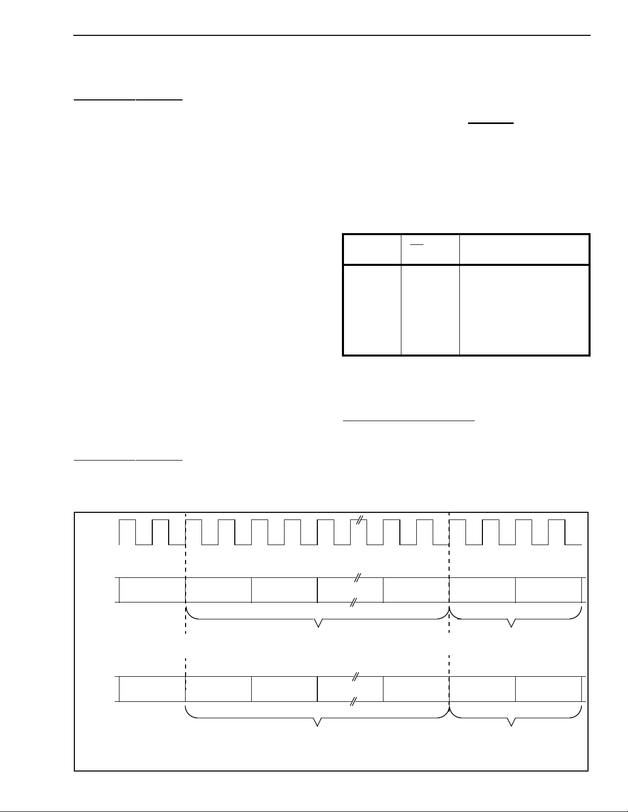
Data Memory Mode-2 is designed for use in
constructing a 1024 by 1024 channel double buff ered
switch. This mode is similar in most respects to Data
Memory Mode-1. The double buffering is achiev ed by
dividing the internal 2048 memory into two equal
blocks. In a single frame, data is written into the first
block and read from the second. In the next frame,
the data will be written into the second and read from
the first (see Figure 6). Frame sequence integrity of
the data will be maintained for all switching
configurations if the output frame is delayed by one
channel with respect to the input frame. In this case,
data clocked into the device during any of the
channels in the current frame will be clocked out in
the next frame. However, if the input and output
frames are aligned, then data switched from any
input channel to output channels 0 or 1 will be
clocked out one frame after the next - consequently
frame sequence integrity is not maintained for
channels 0 or 1. Frame sequence integrity will be
maintained for data switched to any of the other
output channels. (See SMX/PAC Application Note,
MSAN-135, for more information.)
acceptable clock frequency or frame rate. In this
mode, the size of the switching matrix depends on
the clock and frame rates provided as per the
following relationship:
F
=
CK
2 X F
FP
S
where S is the number of channels in the switching
matrix FFP is the frame pulse frequency in Hz, and
FCK is the clock frequency in Hz. The following table
shows how the size of a switching matrix can be
varied by selecting a suitable combination of clock
and frame rates.
CK (MHz) FP (kHz)
16.384
16.384
16.384
12.288
12.288
8.192
8.192
4
8
16
4
8
4
8
Number of channels in
the switching matrix
2,048
1,024
512
1,536
768
1,024
512
It is not possible to switch between Data Memory
Mode-3 and other modes on per-timeslot basis.
It is possible to switch between Data Memory
Mode-1 and Mode-2 on a per timeslot basis.
Data Memory Mode-3
This mode is similar to Data Memory Mode-1.
However, there is no restriction on the minimum
CK
FRAME 1
1
Written to Block 0 Written to Block 1
FRAME 1
Data
Input
Data
Output
FRAME 0
1023
Written to
Block 1
FRAME 0
1023
0
Connect Memory Mode -1
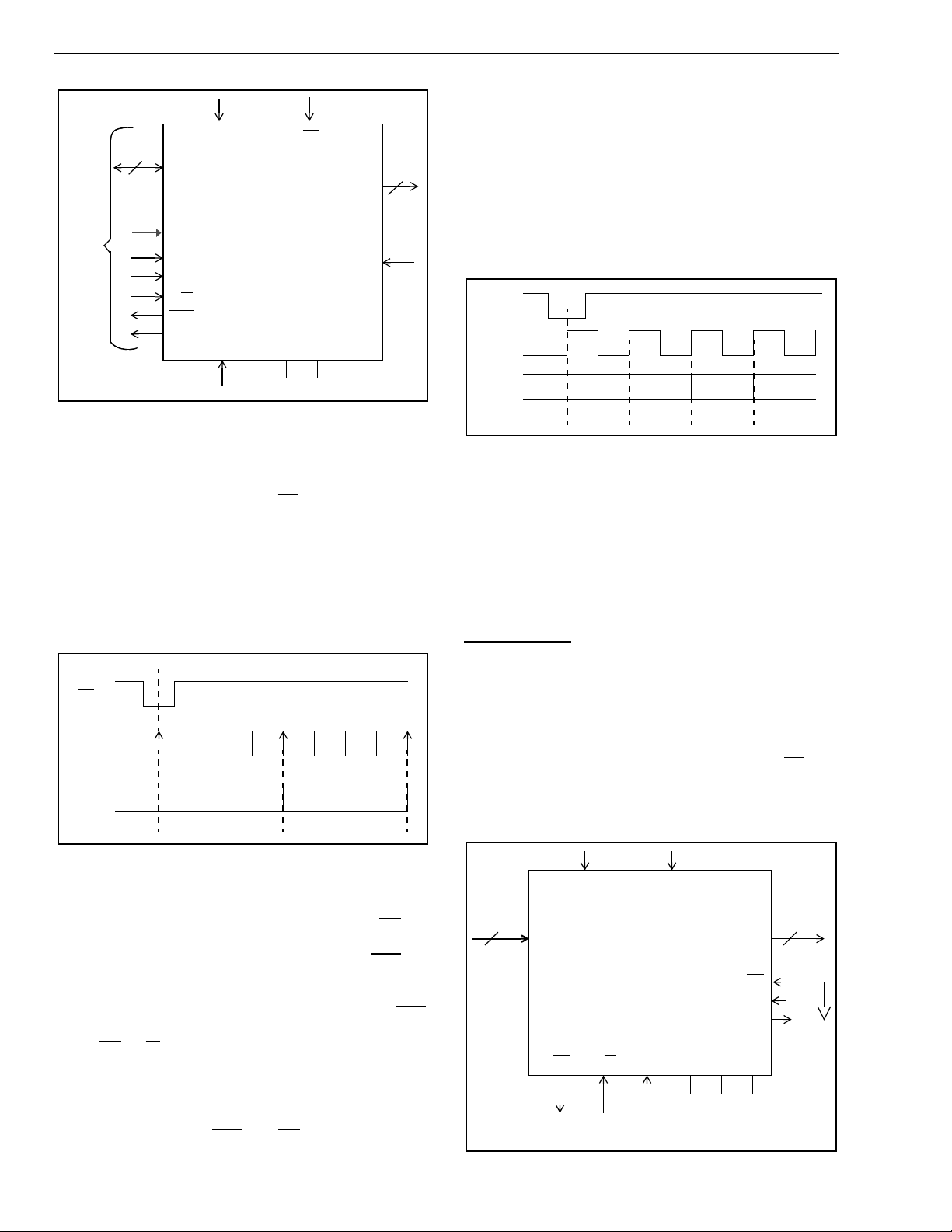
In Connect Memory Mode-1, the input data bus is
bidirectional. Internal memory locations can be
randomly accessed via the microprocessor bus. The
pinout of the device in this mode is illustrated in
Figure 7.
FRAME 2
1023
102301 01
0
1
FRAME 2
Read from
Block 0
Note: No input and output channel alignment is implied in the example shown above. It is assumed that the frame pulse for the
connection memory used to generate adresses for the read operation has a specific phase relationship with respect to the Data
Memory frame pulse.
Read from Block 1 Read from Block 0
Figure 6 - Data Memory Mode-2 Functional Timing
2-107
Page 8
MT9080B CMOS
Connect Memory Mode-2
16
Microprocessor
Interface
CK
D0-D15
A0-A15
CS
DS
W
R/
DTA
CD
ME Z Y X
FP
D0o-D15
MODE
0/1 1 0
16
o
ODE
Figure 7 - Connect Memory Modes Pinout
Data is clocked out on D0o-D15o from memory
locations addressed sequentially by the internal
counter. This counter is incremented every second
clock period and is reset with FP. The frequency of
the clock signal used should be twice the data rate.
A timing diagram showing the relationship between
the data output and the clock signal is presented in
Figure. 8. With a clock rate of 16.384 MHz, the
maximum number of addresses that can be
generated in an 8 kHz frame period is 1024.
Connect Memory Mode-2 is designed specifically for
2048 channel switching applications. Data is clocked
out on D0o-D15o with every rising clock edge from
memory locations addressed sequentially by the
internal counter (see Figure 9). This counter is
incremented with each clock period and is reset with
FP or when a count of 2047 is reached.
FP
CK
DATA
OUTPUT
2047 0 1 2
Fig. 9 - Connect Memory Mode-2 Functional
Timing
The clock frequency should be 16.384 MHz for a
connection memory designed to support a 2048
channel switch.
Microprocessor access is similar to Connect Memory
Mode-1.
Counter Mode
FP
CK
Data
Out
1023 0
Fig. 8 - Connect Memory Mode-1 Functional
Timing
Microprocessor access timing is shown in Figures 28
and 29. During a microprocessor read cycle, DS low
indicates to the SMX that the processor is ready to
receive data. The SMX responds by pulling DTA low
when there is valid data present on the bus. The
processor latches the data in and sets DS high. The
SMX completes the bus cycle by disabling the DTA.
DS should be kept low until afterDT A is issued by the
SMX. CS, R/W and the address lines should also be
asserted for the duration of the access. A MPU write
cycle is similar to the read cycle. Data will be latched
into the device approximately three clock (CK) cycles
after DS goes low. When the device has latched
the data in, it will pull DTA low. DS can subsequently
be set high.
This mode is designed for 2048 channel switching
applications. In the counter mode all read and write
addresses are generated sequentially by the internal
11 bit counter. The 11 bit counter is incremented with
each clock pulse. It will wrap around when it reaches
a count of binary 2047 or when it is reset by FP. The
active input/output pins in this mode are illustrated in
Figure 10.
16
CK
-D15
D0
i
i
CD R/WMEXYZ
FP
D0o-D15
ODE
DTA
100
All other inputs should
be tied Low
CS
o
16
Fig. 10 - Counter Mode Pinout
2-108
Page 9
CMOS MT9080B
The device can perform either a read or a write,
depending on the level asserted at the R/W pin.
When R/W is high, the contents of the memory
addressed by the internal counter will be clocked out
on to the output data bus. Setting R/W low will
enable data on the input data bus to be written into
the device. During a write operation, the output bus
is actively driven by the data latched out in the
previous read operation.
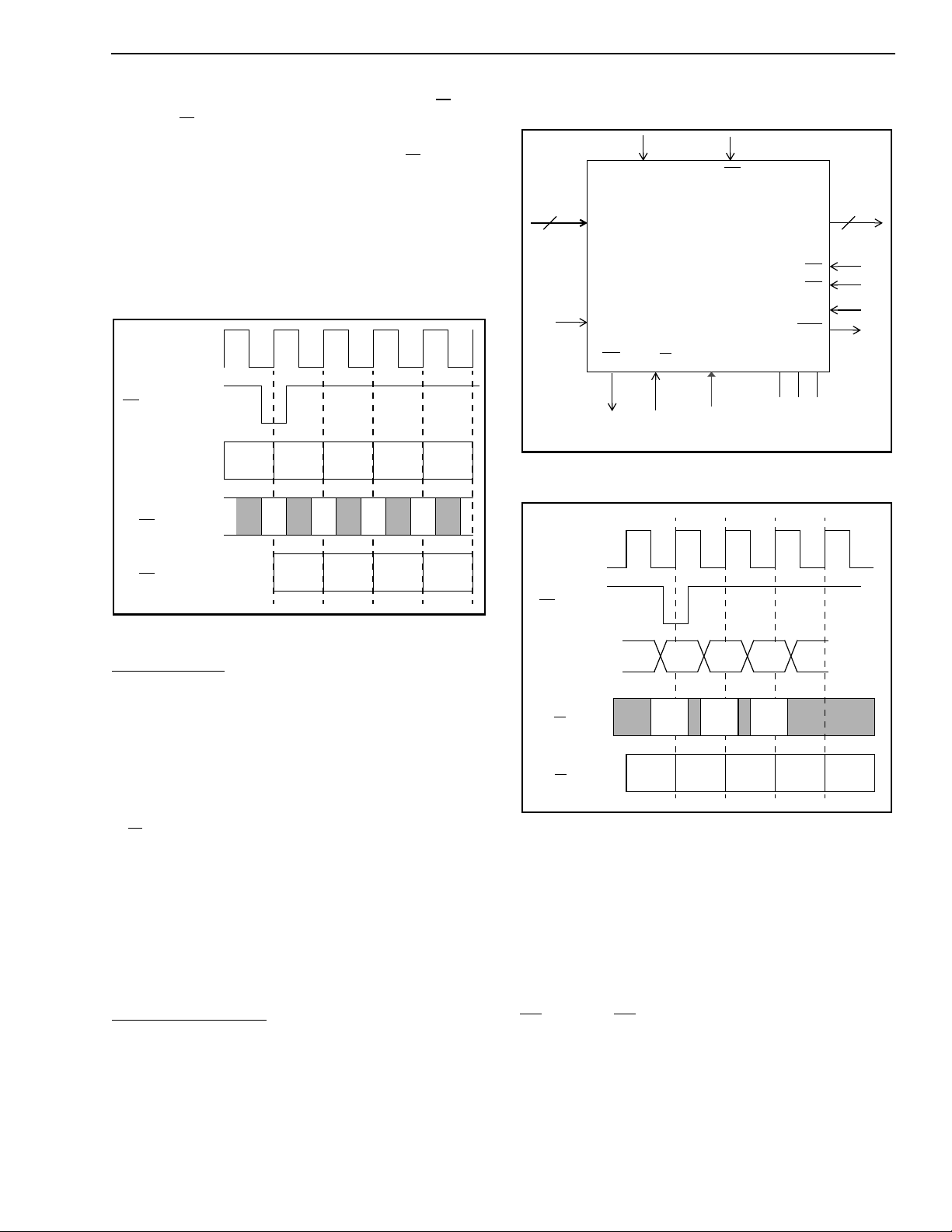
Data is clocked in or out of the device on the positive
edge of the clock. See Figure 11.
CK
FP
Internal
Counter
Data Clocked In
(R/W LOW)
Data Clocked Out
(R/W High)
2047 0 1 2 3
012
2047 0 1 2
3
example, if the address asserted is Hex 02, the delay
through the switch is equal to six clock cycles.
16
D0
ME
CD
-D15
i
CK
i
R/W
FP
A0-A11
All other inputs should
be tied Low
-D15
D0
o
CS
DS
ODE
DTA
101
o
16
XYZ
Figure 12 - External Mode Pinout
CK
Figure 11 - Counter Mode Functional Timing
External Mode
The external mode, which is designed for use in
2048 switching applications, permits random access
to the memory both for input and output operations.
The pinout for external mode is shown in Fig. 12.
The address asserted on the external address bus is
used to specify the memory location to be accessed
for the read or write operation. The level asserted on
R/W during a specific clock period determines
whether the addressed memory is written to or read
from. During a write operation, the output data bus is
actively driven with data latched out in the previous
read operation.
Data is clocked into or out of the device on the
positive edges of the clock as shown in Figure 13.
Shift Register Mode
FP
ADDR
Data In
(R/W Low)
Data Out
(R/W High)
CH X
XYZ
CH Z
CH Y
CH X CH Y CH Z
Figure 13 - External Mode Functional Timing
Maximum permissible delay is equal to 4096 clock
cycles.
The pertinent timing parameters are illustrated in
Figure 14. Data is clocked in and out of the device
with rising edge of the clock.
The address is latched in with the negative edge of
DS while the CS is low.
In this mode, data clocked into the SMX is delayed
by a number of clock cycles before being clocked out
of the device. The delay introduced (in number of
clock cycles) is equal to two times the binary value of
the address latched into the device plus 2. For
2-109
Page 10
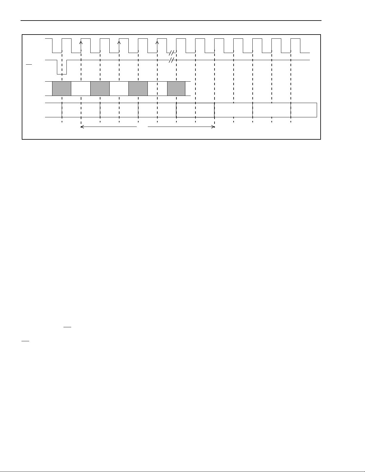
MT9080B CMOS
CK
FP
Data
In
Data
Out
CH X CH Y CH Z
t
td = (Address x 2) + 2 Clock Cycles
d
Figure 14 - Shift Register Mode Data Input/Output Timing
Applications
1024 Channel Switch Matrix
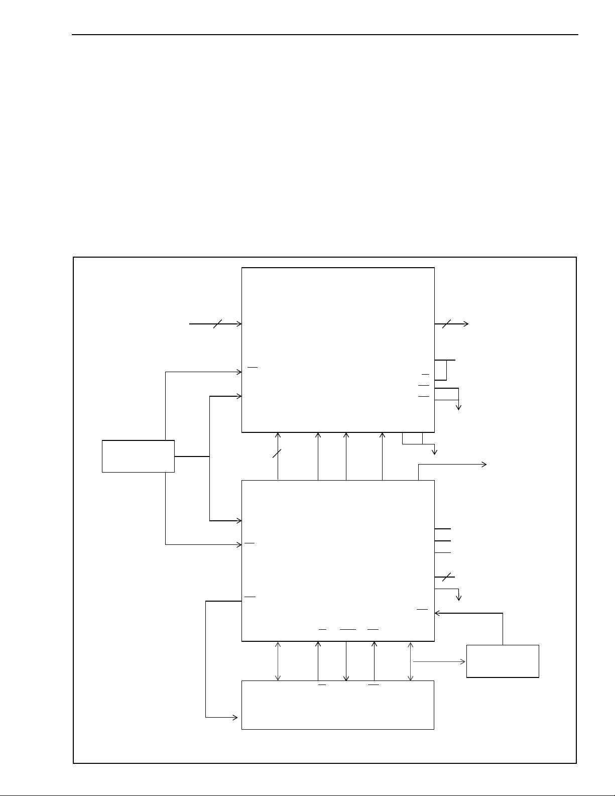
A 1024 channel, non-blocking, timeslot interchange
switch can be constructed using two SMX devices
(refer to Figure 15). One SMX is operated in the Data
Memory mode, while the second device is operated
in Connect Memory Mode-1.
Data to be switched is clocked into the data memory
via the 16 bit input data bus and stored sequentially
in memory locations addressed by the internal 11 bit
counter. The data is read out of the Data Memory
(SMX#1) according to the external address supplied
by the Connection Memory (SMX#2). The
Connection memory clocks out contents of the
memory according to the addresses supplied by the
internal counter.
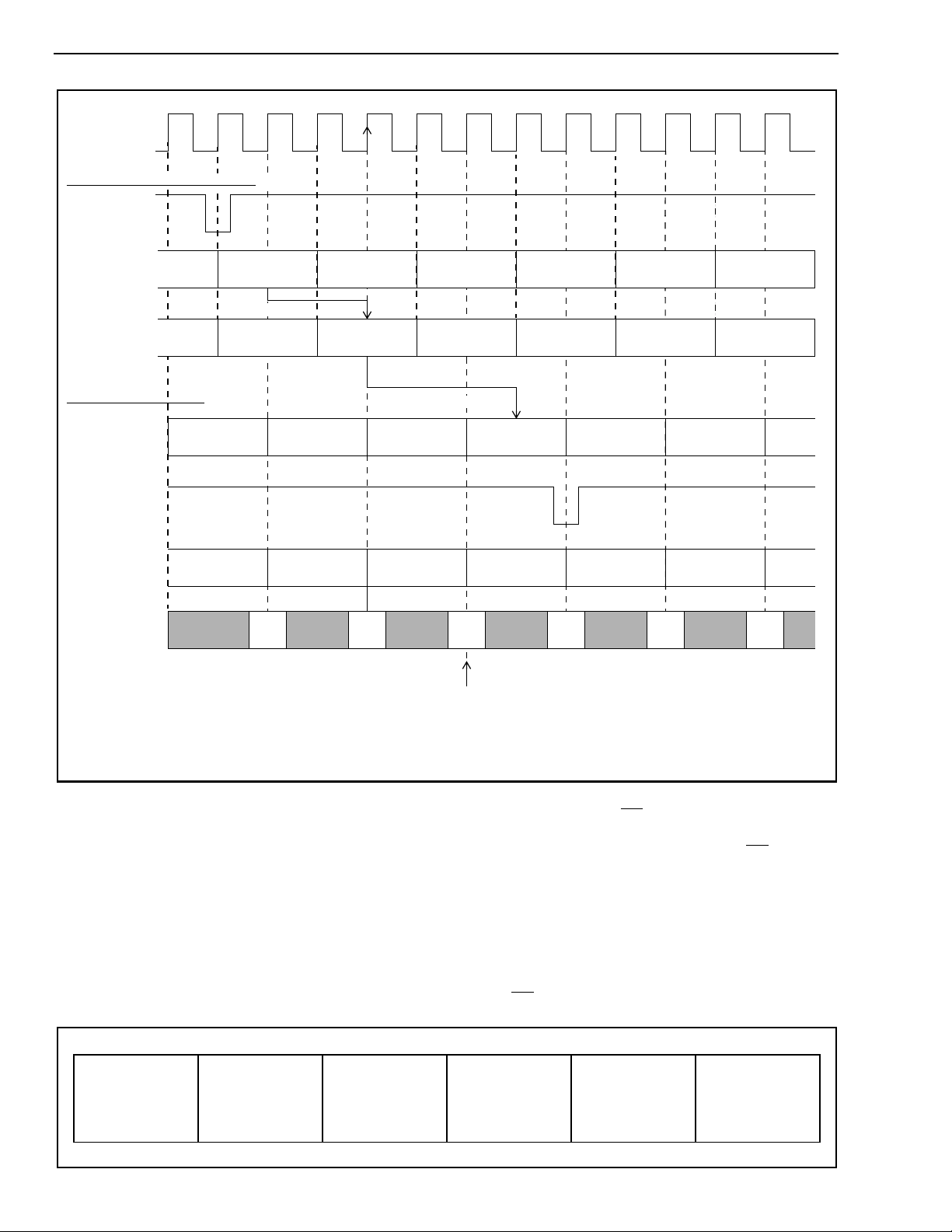
The clock applied at the CK input of both the devices
has a frequency of 16.384 MHz. There are two clock
periods in each channel timeslot (see Figure 16). A
framing signal (FP) with a frequency of 8 kHz is used
to delineate frames with 1024 channels each. The
FP input to the Data Memory is delayed by seven
clock periods from the Connection Memory frame
pulse. This phase delay synchronizes the internal
counters of the two SMXs such that the Connection
Memory clocks out addresses one channel ahead of
the affected timelsot.
Using the connections illustrated in Figure 15, the
Data Memory address and control functions can be
mapped onto specific bits of the Connect Memory to
form a 16 bit control word, as shown in Figure 17.
CH X CH Y CH Z
counter, this word will be clocked out of the memory
on to the data bus (D0o-D15o).
The output on the Connect Memory data bus
(D0o-D9o) is used to specify the Data Memory
location to be read out during any particular timeslot.
The Connection Memory is programmed in a manner
that permits specific addresses to be output in
certain timeslots. The Data Memory will clock out
data from internal memory locations according to the
address asserted on its address bus. As mentioned
earlier, this address is latched into Data Memory with
a positive edge of the clock. The contents of the
appropriate addressed memory location will be
clocked out of the device at the beginning of the next
channel timeslot.
Connection Memory bit 10 controls the level on the
ODE input. The ODE pin is used to enable the output
drivers of the Data Memory. The capability to
selectively enable or disable the output drivers
during specific channel timeslots is required when
constructing larger switches using the 1024 channel
switch as a building block.
The Message Enable (ME) input of the Data Memory
is controlled by D11. Setting this particular bit high
will result in the data latched into the address bus
being clocked out on to the Data Memory output bus.
Note that only 10 of the 16 address inputs are
actually connected to the data bus of the Connection
Memory. Consequently, only 10 of the 16 data output
bits on the Data Memory can be dynamically
controlled through the Connection Memory. In other
applications, all 16 of the address bits may be
connected to the data output bus of the Connection
Memory.
The 16 bit control word is written into the Connection
Memory by the processor. Subsequently, when the
memory location is addressed by the internal
2-110
The mode of operation of the Data Memory can be
changed from Data Memory Mode-1 to Data Memory
Mode-2 by setting or resetting D12 in the connection
Page 11
CMOS MT9080B
memory. The delay through the matrix can be
optimized for specific applications by selectively
enabling one of the two modes. Data Memory-1
(DM-1) is designed for voice switching applications
where it is generally desirable to minimize delay
through the switch. As mentioned earlier in the DM-1
description, the delay through the switch depends
upon the difference between the input channel
timeslot and the output channel timeslot.
Consecutive output channels switched from
non-contiguous input channels will not always
originate from the same input frame. For example, if
channels 3, 6 and 8 are to be switched to channels 5,
6 and 7; output channel 5 will contain data input in
the current frame, while channels 6 and 7 will contain
data clocked in one frame earlier. Data Memory-2
Parallel Input Data
16
D0
-D15
i
i
(DM-2) is designed for data switching applications
where concatenation of a number of channels is
often necessary. Data clocked out of the device will
originate from the previous frame, regardless of the
input/output time difference. There is one exception,
when channel 1023 is switched to channel 0, the
contents of Channel 0 will not originate from the
previous frame but rather from the frame before it.
The capability to selectively change between DM-1
and DM-2 allows a single switch to handle both voice
and data effectively.
External bus drivers can be controlled with D13 of
the Connection Memory data bus. This bit will be
output along with the remaining bits one channel
SMX #1
DM-1/2
DAT A
MEMORY
D0o-D15
o
Parallel Output Data
16
Timing
Generator
FP#1
FP#2
CK
FP
CK
A0-A9 ODE ME Z Y X
10
D0
-D9oD10oD11
o
CK
SMX #2
FP
CD
D0-D15 R/W DTA DS A0-A9
CM-1
CONNECTION
MEMORY
D12
o
A10-A15
MODE
o
MODE
A11-A15
R/
D13
A10
CS
DS
CS
+5
W
External
Tristate
Control
o
X
Y
Z
0
1
0
+5
D0-D15 R/
IRQ
Note: All other inputs not shown in this diagram should be connected to GND.
W HALT DS
16-BIT MPU
Figure 15 - 1024 Channel Switch Matrix
Address
Decode
2-111
Page 12
MT9080B CMOS
CK
CONNECTION MEMORY TIMING
FP #2
Internal
Counter
(Read
Address)
Data Output
D0o-D15o
1023 0 1 2 3 4 5
1022 1023 0 1 2 3 4
➀②➂➃
addresses
DATA MEMORY TIMING
Data Output
D0o-D15o
FP #1
Internal Counter
(Write Address)
Data In
D0i-D15i
Note 1: Address is latched into the Data Memory by the first positive clock edge in a timeslot (edge ➀ for Ch. 0). Data will be
clocked out by the first positive clock edge in the next timeslot (edge ② for Ch. 0).
Note 2: Data is latched into the Data Memory by the first rising edge in a timeslot (edge ➂ for Ch. 0) and is written into the
memory location addressed by the internal counter with the next rising edge (edge ➃ for Ch. 0).
1021 1022 1023 0 1 2 3
1021 1022 1023 0 1 2
1021 1022 1023 0 1 2
SMX #1 Data Input/Output Frame Boundary
addresses
Figure 16 - 1024 Channel Switch Timing
ahead of time; i.e., one channel before the
addressed data is clocked out of the Data Memory. It
may be necessary to provide an external bus enable
one channel ahead of time in applications where
precharging of the external data bus is required. In
other applications where no precharge is required,
control bit from the next channel may be used in
order to ensure that the external bus is enabled at
the same time as the channel is being clocked out of
the device.
The Change Detect (CD) output of the Connection
Memory is used to interrupt the MPU. As mentioned
in the Pin and Functional descriptions, CD goes low
when the internal CRC performed by the device
indicates a change in memory contents. This feature
is particularly useful in switching applications where
the Connection Memory is configured once and is
not modified for long periods of time, e.g., in network
digital access crossconnect systems. Any
inadvertent corruption of the memory contents will
cause CD to interrupt the processor.
2-112
D15 - D14
Unused
D13
External
Driver
Enable
D12
DM-1 or
DM-2
Select
D11
Message
Enable
D10
ODE
Control
D9 - D0
Source
Channel
Address
Figure 17 - Mapping of Address and Control Signals onto Connect Memory Data Bits
Page 13
CMOS MT9080B
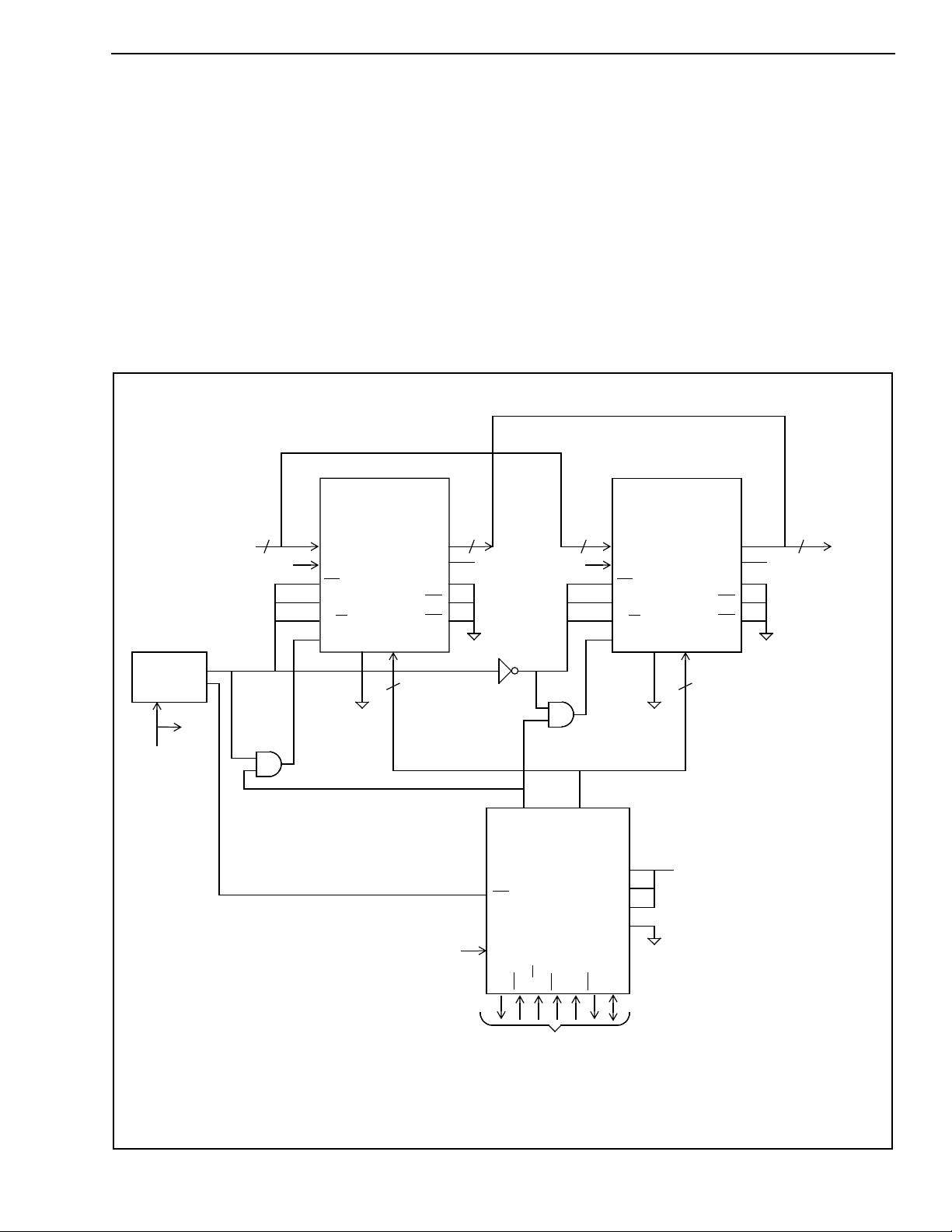
Switching any input channel to an output channel
timeslot is possible by merely writing the address of
the input channel in the Connection Memory location
corresponding to the output channel timeslot. For
example, to switch channel 1 to output channel 5 and
enable output drivers during channel 5, the
Connection Memory location corresponding to
channel 5 should be loaded with Hex 2001. This
word will be clocked out of the Connection Memory
during timeslot 4 and will cause the Data Memory to
clock out contents of the memory corresponding to
channel 1 during the channel 5 timeslot. The 16 bit
word clocked out b y the Connection Memory will also
enable Data Memory output drivers, and, external
drivers.
CNT/EXT
SMX #1
Timing
Generator
16
C16
D0-D15i
CK
FP
Mz
R/
W
ODE
DATA
MEMORY
ME
D0-D15o
Mx
My
CS
DS
A0-A10
2048 Channel Switch Matrix
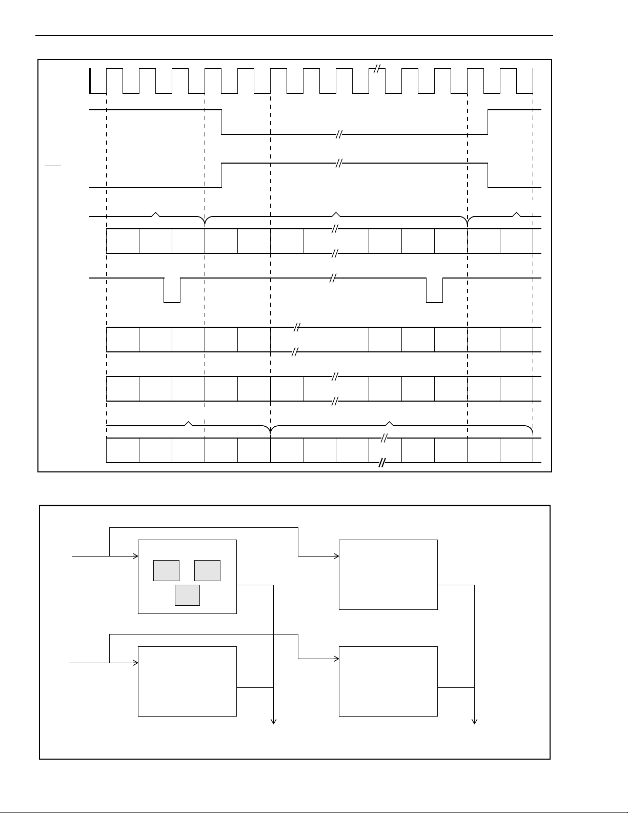
A 2048 channel, double buffered timeslot
interchange switch can be constructed with three
SMXs as shown in Figure 18. SMX#1 and SMX#2
are used to store data and switch it in time, while the
third SMX functions as a Connection Memory.
SMX#1 and 2 are operated in the Counter Mode and
External Mode alternatively in consecutive frames. In
any specific frame, one of the two is in Counter mode
while the other is in External mode. The functions
are reversed in the successive frame. The SMX in
counter mode is programmed to write data
CNT/EXT
SMX #2
161616
+5
+5
C16
D0-D15i
CK
FP
Mz
R/
W
ODE
ME
D0-D15o
DATA
MEMORY
A0-A10
Mx
My
CS
DS
Data
Output
DFP
CFP
C16
16.384 MHz
Notes:
1) U1 and U2 are required if the data output bus is to be enabled/disabled via the microprocessor interface.
2) All inputs not shown should be connected to Ground (V
U1
11
C16
SS
D11 D0o-D10o
FP
CK
DTADSR/W
).
U2
CM-2
SMX #3
CONNECTION
MEMORY
CS
A0-A15CDD0-D15
MPU Interface
ODE
Mz
My
Mx
11
+5
Figure 18 - 2048 Channel Timeslot Interchange Circuit
2-113
Page 14
MT9080B CMOS
CK
DFP
(SMX #1)
DFP
(SMX #2)
Data In
(SMX1/2)
CFP
(SMX #3)
SMX #3
Int. Counter
SMX #3
D0o-D10o
Data Out
(SMX 1/2)
Written to SMX #2 Written to SMX #1
2045
2046 2047 012
2044 2045 2046 2047 0 1 2 2044 2045 2046 2047
01 2
Read from SMX #1
2045
2046 2047
Read from SMX #2
Written from SMX #2
012046 20472046 2047 0 1 2
0122045 2046 2047 0 1 2045 2046 2047
Figure 19 - 2048 Channel Switch Timing
Data
Data
2-114
In
In
CH 2,049-4,096
CH 1-2,048
LARGE MATRIX 1
DM
LARGE MATRIX 3
DM
CM
Figure 20 - Extended Switching Matrix
ODE
ODE
LARGE MATRIX 2
ODE
LARGE MATRIX 4
ODE
CH 1-2,048
Data Out Data Out
CH 2,049-4,096
Page 15
into its memories addressed by the internal counter.
The SMX in the external mode reads data out from
memory locations addressed by the Connection
memory. In this manner, incoming data is continually
written into one memory block while it is being read
out of the other block. The device in counter mode
has its output drivers disabled.
This configuration results in a maximum throughput
delay of two frames. Data clocked into the device in
the current frame is clocked out in the next frame.
The appropriate timing parameters are illustrated in
Figure 19. The clock signal applied to all three SMXs
has the same frequency.
SMX#3 is operated in Connect Memory Mode-2. In
this mode, data is clocked out of the device at the
same rate as the clock, i.e., at 16.384 Mbps.
Extended Switching Matrix
16
Address
Decode
CK FP
D0-D15i
Z
Y
X
CS
A0-A11
ADDRESS
CMOS MT9080B
DM-1/DM-2
DS
DTA
DS HALT IRQ
M P U
ODE
D0-D15o
CD
R/
+5V
D0-D15
W
+5V
16
Larger extended switch matrices can be created
using the 1024/2048 channel switch as a building
block. As shown in Figure 20, a 4096 channel matrix
would require four smaller 2048 channel building
blocks.
Construction of matrices larger than 4K may require
external drivers to accommodate the greater
capacitive loading on the outputs.
Using the SMX for Messaging
In some system architectures the PCM voice signals
and system status information is transmitted and
received over a common backplane. To facilitate
microprocessor access to the backplane, the SMX
can be used to read incoming data or write to a
channel on the output data bus.
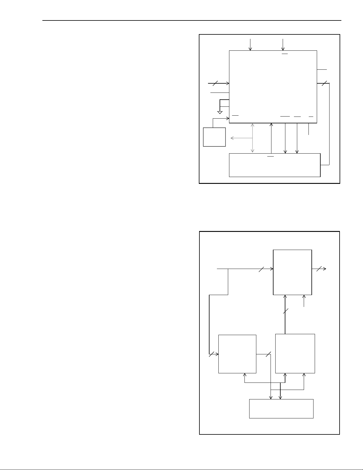
Data clocked into the SMX can be read from the
device by a microprocessor interfaced to the output
data bus and the address bus (see Figure 21). Data
can be written to a specific timeslot on the output
data bus directly by the microprocessor using the
messaging feature (enabled by tying the ME pin
high).
Figure 21 - Reading the Data Memory with a
Microprocessor
SMX. The data output bus of the third SMX is
connected to the data bus of the MPU.
SMX #1
DATA MEMORY
Data in
16
16
SMX #3
MESSAGING
DM-1 CM-1/2
D0
D0
D15
-
i
i
D15
ADDR
-
o
o
16
DM-1/2
ADDR
16
SMX #2
CONNECTION
MEMORY
ADDR DATA
Data out
16
ME
+5V
A 1024 Switch Matrix with messaging capability can
be constructed with three SMXs as shown in Figure
22. The first SMX is used for performing the actual
switching function. The second SMX is configured as
the connection memory. As discussed in the 1024
switch application, by enabling the messaging
feature, data clocked out of the connection memory
and latched into the data memory address bus will
be clocked out on to the data bus directly. Incoming
data is read by the microprocessor using the third
ADDRDATA
MPU
Figure 22 - A 1024 Channel Switch Matrix with
Message Capability
2-115
Page 16
MT9080B CMOS
Parallel-to-Serial Conversion
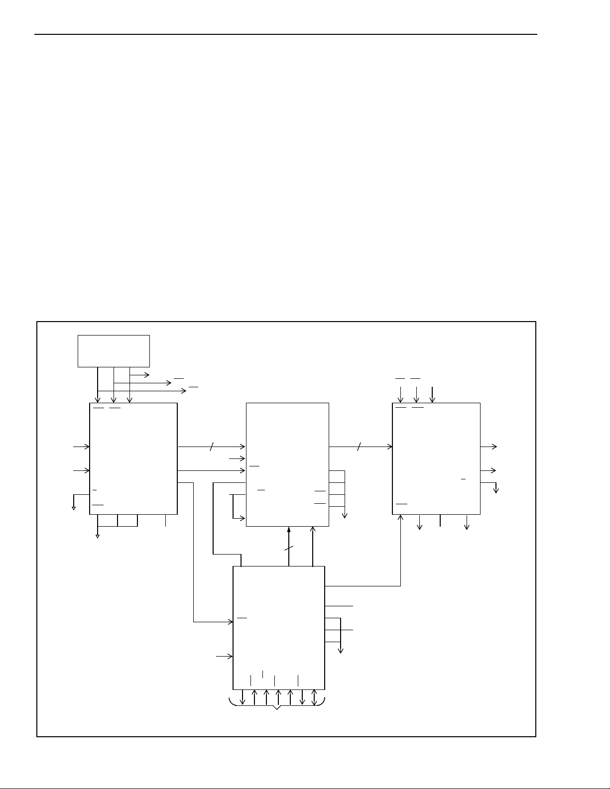
The SMX can be used in systems which employ
serial architectures by converting the parallel I/O into
a serial format. The Mitel MT9085 Parallel Access
Circuit (PAC) is designed to interface to the parallel
busses of the SMX. A single PAC can convert the
output of a1024 channel switch into 2.048 Mbit/s or
4.096 Mbit/s serial format. A second PAC can be
configured to implement serial to parallel conversion
(see Figure 23).
The PAC generates all framing signals required to
implement a 1024 or 2048 channel matrix. Refer to
the MT9085 data sheet for more information on
operation of the PAC.
For more information, see Mitel’s Application Note
MSAN-135
Matrices using the SMX/PAC“
“Design of Large Digital Switching
.
S0
S31
Timing
Source
C16
C4
F0
C4i C16i
F0i
PAC
CKD
S/P
MCA
P0-P7
DFPo
CFPo
MCB
+5
S0
•
•
•
•
•
•
•
•
S31
2/4S
OE
C16
8
C16
+5
D12 D0-D9 D11
FP
CK
SMX #1
DM - 1/2
D0-D7i
CK
FP
MEMORY
Mz
W
R/
ODE
SMX #2
CM - 1
CONNECTION
MEMORY
DATA
A0-A9
D0-D7o
ME
10
D10
ODE
Mx
My
Mz
8
Mx
My
CS
DS
+5
+5
F0 C4 C16
F0i C4i C16i
PAC
P/S
P0-P7
OE
CKD
MCA
+5
S31
2/4S
MCB
S0
S0
•
•
•
•
•
•
•
•
S31
2-116
DTADSR/W
CS
A0-A15CDD0-D15
MPU Interface
NOTE: Connect all inputs not shown to V
Figure 23 - 1024 Channel Serial Switch Matrix Using the PAC and SMX
SS
Page 17
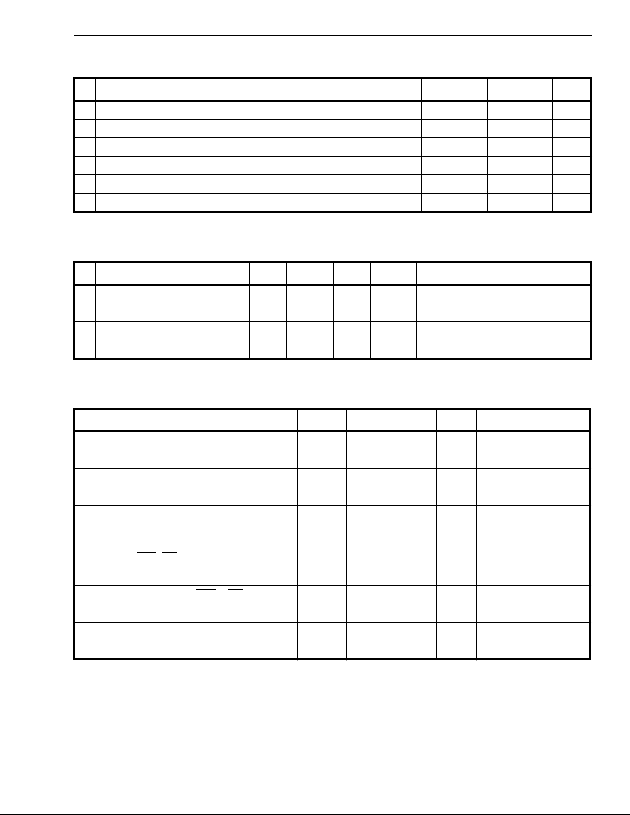
Absolute Maximum Ratings*
Parameter Symbol Min Max Units
CMOS MT9080B
1 Supply Voltage VDD-V
SS
2 All Input Voltages V
3 All Output Voltages V
4 Storage Temperature Range T
5 Current at Digital Outputs I
6 Continuous Power Dissipation P
* Exceeding these values may cause permanent damage. Functional operation under these conditions is not implied.
Recommended Operating Conditions - Voltages are with respect to Ground (V
Characteristics Sym Min Typ
1 Supply Voltage V
2 Operating Temperature T
3 Input High Voltage V
4 Input low Voltage V
‡ Typical figures are at 25°C and are for design aid only: not guaranteed and not subject to production testing.
DD
OP
IH
IL
4.75 5.0 5.75 V
-40 70 °C
0.7V
DD
0 0.3V
DC Electrical Characteristics - Voltages are with respect to Ground (V
Characteristics Sym Min Typ
V
DD
i
o
S
O
D
‡
Max Units Test Conditions
-0.3 7 V
VSS-0.3 VDD+0.3 V
VSS-0.3 VDD+0.3 V
-40 125 °C
) unless otherwise stated.
SS
V
DD
) unless otherwise stated.
SS
‡
Max Units Test Conditions
V
150 mA
2W
1 Supply Current I
2 Input High Voltage V
3 Input Low Voltage V
4 Input Leakage Current I
5 Output High Current (all outputs
I
DD
IL
OH
0.7V
IH
IL
DD
0 0.3V
8mAV
120 200 mA Outputs unloaded
V
DD
V
±10 µA
except D0i-D15i)
6 Output Low Current (all outputs
I
OL
8mAV
except DTA, CD and D0i-D15i)
7 Output High Current D0i-D15i I
8 Output Low Current DTA & CD I
9 Input Capacitance C
10 Output Pin Capacitance C
11 High Impedance Leakage I
‡ Typical figures are at 25°C and are for design aid only: not guaranteed and not subject to production testing.
OH
OL
i
o
OZ
2mAV
2mAV
10 pF
10 pF VDD=5.0V±10%.
10 µA
OH
OL
OH
OL
=0.7 V
=0.3 V
=0.7 V
=0.3 V
DD
DD
DD
DD
2-117
Page 18
MT9080B CMOS
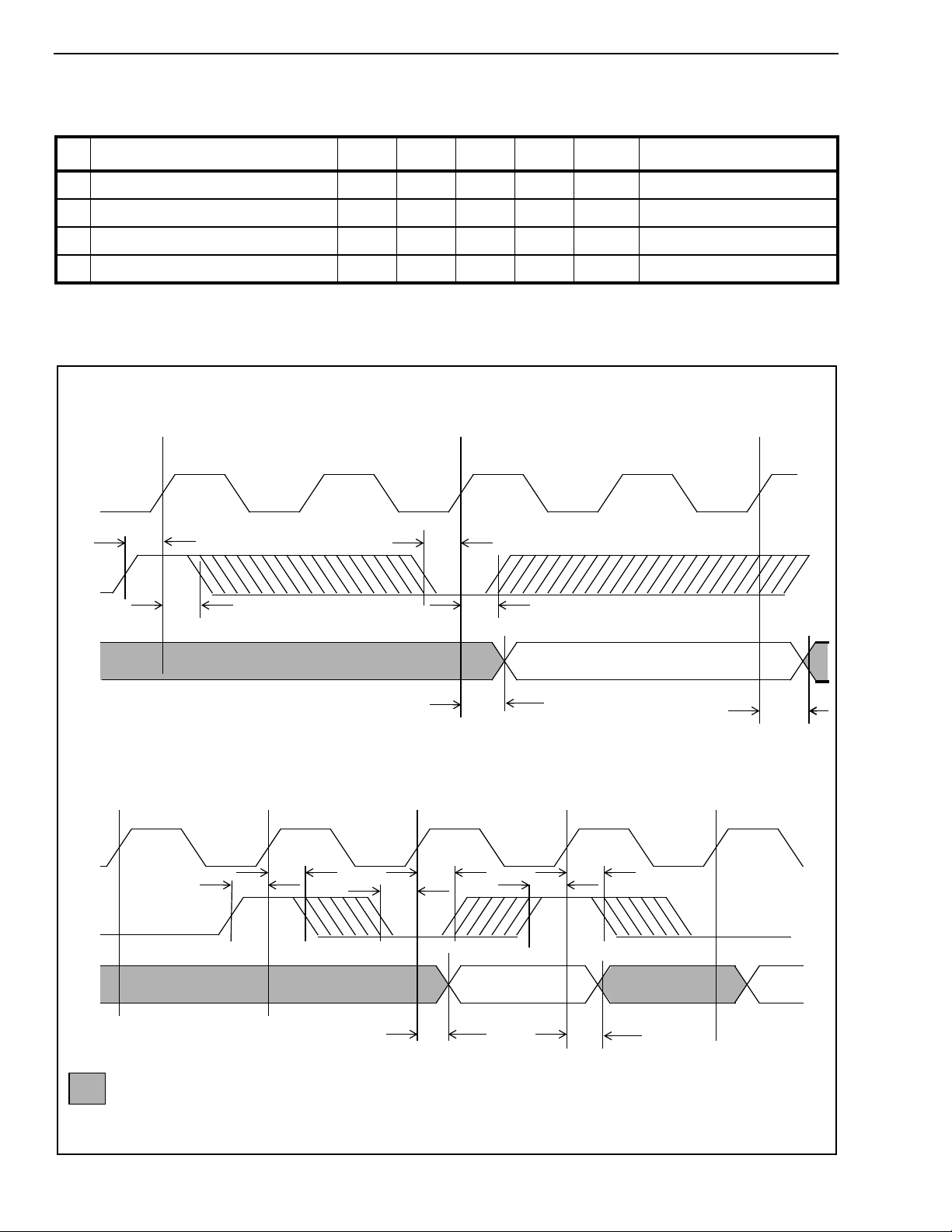
AC Electrical Characteristics†- Output Drive Enable Timing (see Fig. 24) - Voltages are with respect
to Ground (V
) unless otherwise stated.
SS
Characteristics Sym Min Typ
‡
Max Units Test Conditions
1 ODE Setup t
2 ODE Hold t
3 Data Output High Z to Active t
4 Data Output Active to High Z t
† Timing is over recommended temperature and power supply voltages.
‡ Typical figures are at 25°C and are for design aid only; not guaranteed and not subject to production testing.
OS
OH
DZA
DAZ
0ns
20 ns
35 ns CL=30pF
30 ns
1. Data Memory Modes And Connect Memory Mode - 1
CHANNEL N CHANNEL N + 1
CK
ODE
D0oD15o
t
OS
t
OH
t
OS
t
OH
t
DZA
t
DAZ
90%
10%
2. Counter, External And Connect Memory Mode - 2
CK
ODE
D0oD15o
CHANNEL CHANNEL
N N + 2
t
OS
HIGH IMPEDANCE STATE - OUTPUT DRIVERS DISABLED
t
OH
CHANNEL
N + 1
t
OS
Figure 24 - Output Drive Enable Timing
2-118
t
t
OH
DZA
t
OH
t
OS
90%
10%
t
DAZ
Page 19
CMOS MT9080B
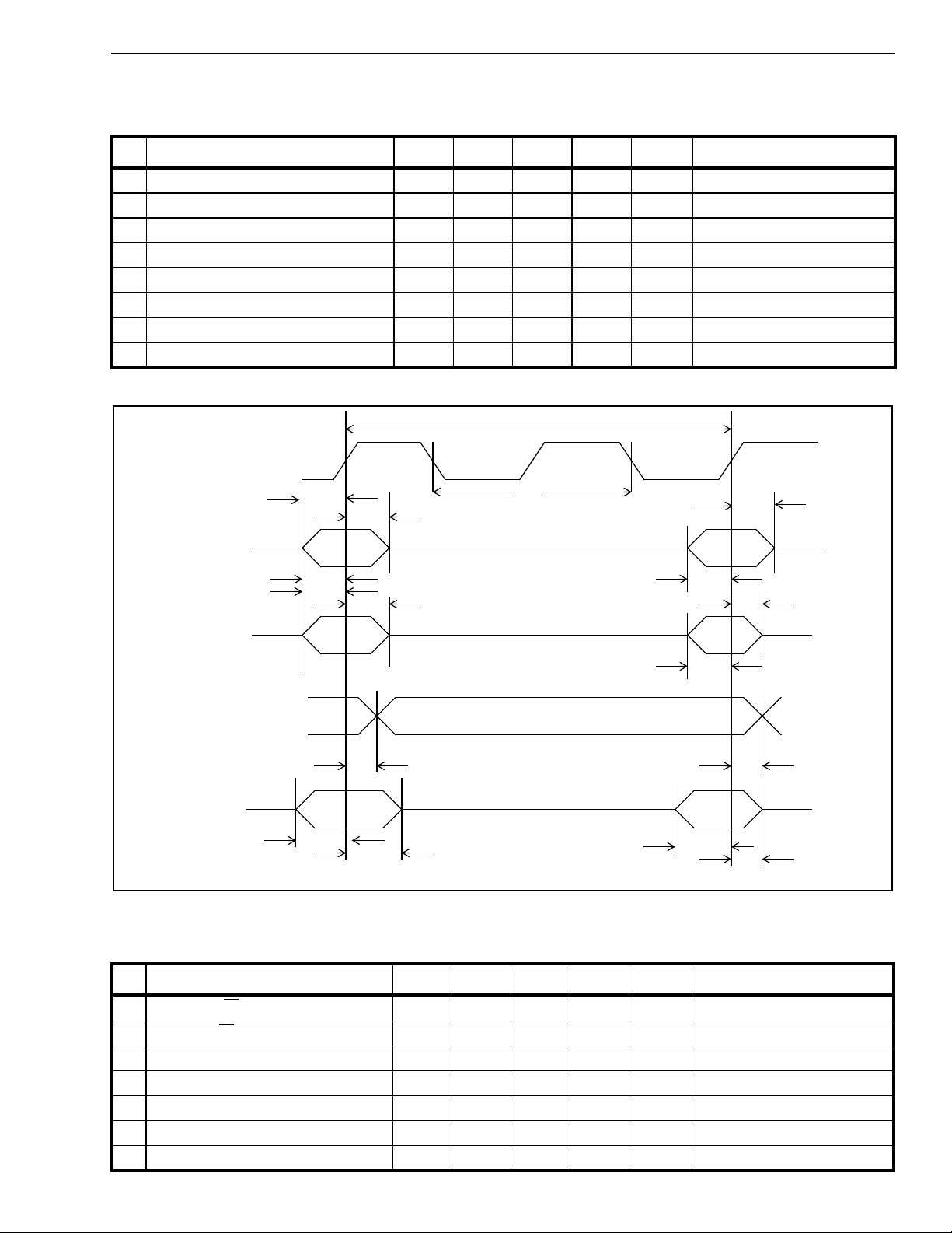
AC Electrical Characteristics†- Data Memory, Connect Memory-1 and Shift Register
Mode Timing (See Fig. 25) - Voltages are with respect to Ground (V
Characteristics Sym Min Typ
) unless otherwise stated.
SS
‡
Max Units Test Conditions
1 Address Setup t
2 Address Hold t
3 Data Output Delay t
4 Data Input Setup t
5 Data Input Hold t
6 ME, Mx, My, Mz Setup t
7 ME, Mx, My, Mz Hold t
8 CK Clock Period t
† Timing is over recommended temperature and power supply voltages.
‡ Typical figures are at 25°C and are for design aid only; not guaranteed and not subject to production testing.
CK
A0-A15*
t
t
MES
AS
t
AS
AS
AH
DD
DS
DH
MES
MEH
PCK
t
t
AH
MEH
0ns
18 ns
934nsC
2ns
4ns
0ns
26 ns
60 ns
Channel Timeslot
t
PCK
t
AS
= 30 pF
L
t
MEH
t
AH
ME/Mx/y/z
t
MES
D0o-D15o
t
DD
D0i-D15i*
t
DS
*Timing applicable to Data Memory and Shift Register modes only.
t
DH
t
DS
t
DD
t
DH
Figure 25 - Data Memory, Connect Memory-1 and Shift Register Mode Timing
AC Electrical Characteristics†- External, Connect Memory-2 and Counter Mode Timing
(See Fig. 26) - Voltages are with respect to Ground (V
Characteristics Sym Min Typ
1 ADDR, R/W Hold Time t
2 ADDR,R/W Setup Time t
3 Data Setup t
4 Data Hold t
5 Data Output Delay t
6 ME, Mx, My, Mz Setup t
7 ME, Mx, My, Mz Hold t
† Timing is over recommended temperature and power supply voltages.
‡ Typical figures are at 25°C and are for design aid only; not guaranteed and not subject to production testing.
WEH
WES
DS
DH
DD
MES
MEH
) unless otherwise stated.
SS
‡
Max Units Test Conditions
10 ns
2ns
2ns
4ns
934nsC
= 30 pF
L
0ns
26 ns
2-119
Page 20
MT9080B CMOS
CK
A0-A15*,
W**
R/
ME/Mx/y/z
t
WES
Channel Timeslot
t
WEH
t
WES
t
WEH
D0i-D15i**
D0o-D15o
t
MES
***Timing applicable to External mode only.
Timing applicable to External and Counter modes.
t
MEH
t
DS
t
DH
t
DD
t
MES
t
MEH
t
DS
t
DH
t
DD
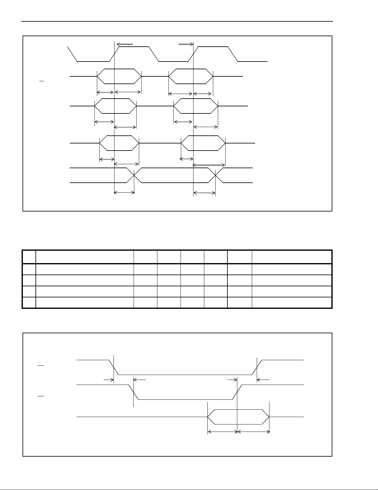
Figure 26 - External, Connect Memory-2 and Counter Mode Timing
AC Electrical Characteristics† - Address Bus Timing In Shift Register Mode (See Fig. 27) -
Voltages are with respect to Ground (VSS) unless otherwise stated.
Characteristics Sym Min Typ
1 Address Setup t
2 Address Hold t
3 Chip Select Setup t
4 Chip Select Hold t
† Timing is over recommended temperature and power supply voltages.
‡ Typical figures are at 25°C and are for design aid only; not guaranteed and not subject to production testing.
AS
AH
CSS
CSH
0ns
12 ns
0ns
0ns
‡
Max Units Test Conditions
2-120
CS
DS
A0-A15
t
CSS
t
AS
t
CSH
t
AH
Figure 27 - Address Bus Timing in Shift Register Mode
Page 21
CMOS MT9080B
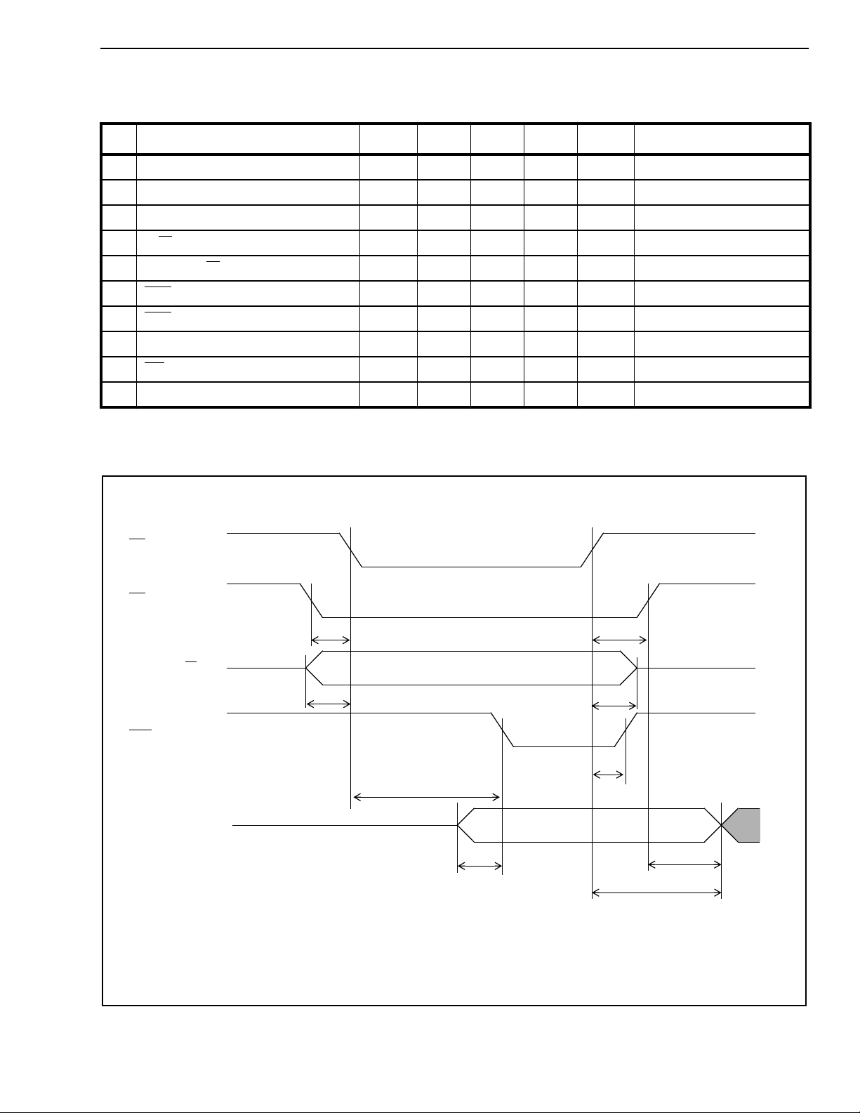
AC Electrical Characteristics† - Microprocessor Read Timing for Connect Memory, Data
Memory & External Modes (See Fig. 28) - Voltages are with respect to Ground (V
Characteristics Sym Min Typ
‡
Max Units Test Conditions
) unless otherwise stated.
SS
1 Chip Select Setup t
2 Chip Select Hold t
3 ADDR t
4R/W Setup t
5 ADDR, R/W Hold t
6 DTA Delay t
7 DTA Hold t
8 Valid Data Out to DTA Low t
9 DS High to Data Invalid t
10 Output Data Active to High Z t
*TCK= Clock (CK) Period
† Timing is over recommended temperature and power supply voltages.
‡ Typical figures are at 25°C and are for design aid only; not guaranteed and not subject to production testing.
DS
CSS
CSH
AS
AS
AH
DTAD
DTAH
RD
DH
DHZ
0ns
0ns
0ns
3ns
0ns
4.5 9 TCK*
0ns
3T
CK
*
027ns
31 ns
CS
t
CSS
A0-A15, R/W
t
AS
DTA
t
DTAD
Data Bus*
t
RD
In Data Memory Mode and External Mode, data is clocked out on D0o-D15o; in Connect Memory Mode data is clocked out on
*
D0i-D15i (bidirectional).
t
DTAH
t
t
AH
CSH
t
DHZ
t
DH
Figure 28 - Microprocessor Read Timing for Connect Memory Mode, Data Memory Mode and
External Mode
2-121
Page 22
MT9080B CMOS
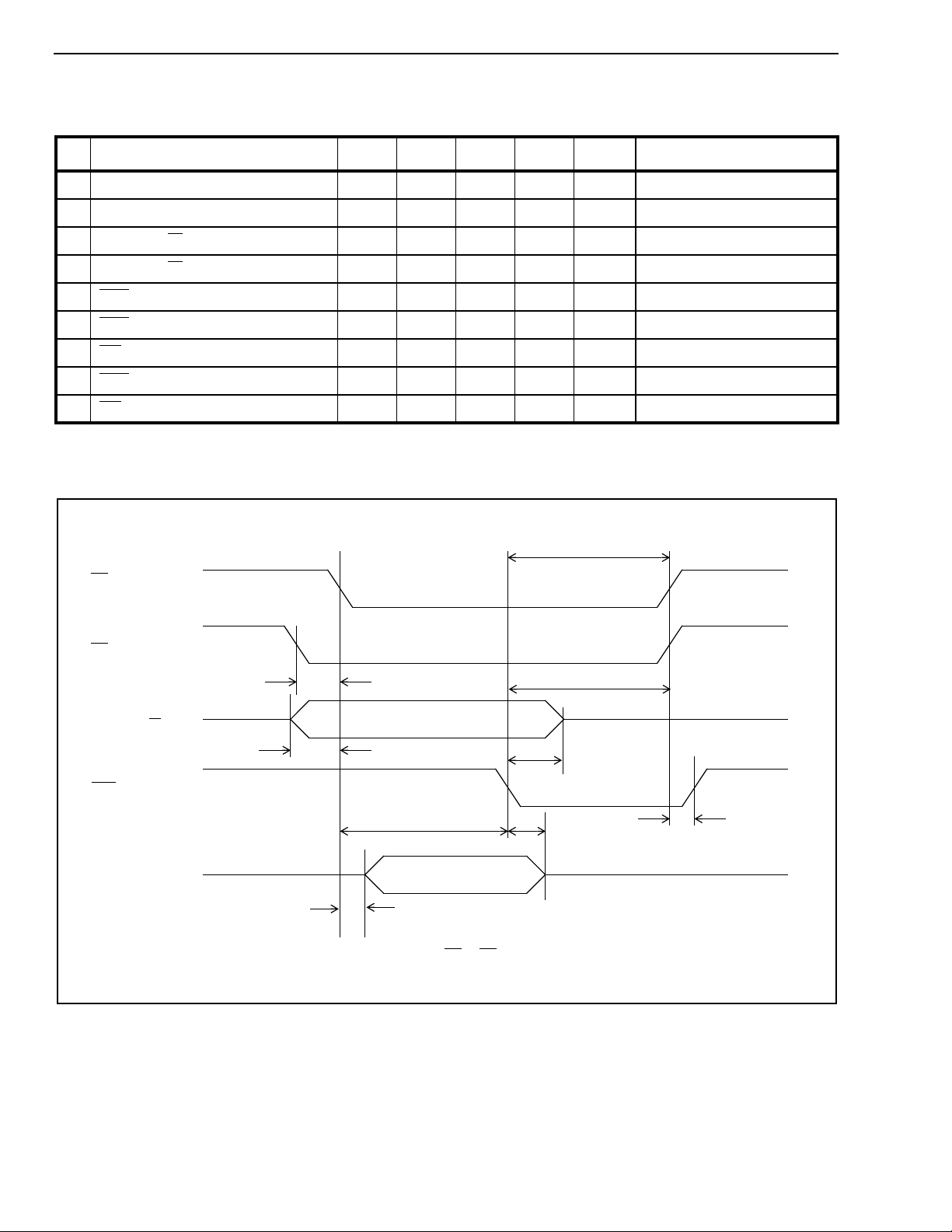
AC Electrical Characteristics† - Microprocessor Write Timing for Connect Memory Mode
(See Fig. 29) - Voltages are with respect to Ground (V
Characteristics Sym Min Typ
) unless otherwise stated.
SS
‡
Max Units Test Conditions
1 Chip Select Setup t
2 Chip Select Hold t
3 ADDR, R/W Setup t
4 ADDR, R/W Hold t
5 DTA Delay t
6 DTA Hold t
7 DS Low to Data in Delay t
8 DTA Low to Data in Hold t
9 DS Hold Time t
*TCK= Clock (CK) Period
† Timing is over recommended temperature and power supply voltages.
‡ Typical figures are at 25°C and are for design aid only; not guaranteed and not subject to production testing.
DS
CSS
CSH
AS
AH
DTAD
DTAH
DD
DH
DSH
0ns
0ns
0ns
0ns
4.5 7.5 TCK*
0ns
4.5 TCK*
0ns
0ns
t
DSH
CS
AH
t
CSH
t
CSS
A0-A15,R/
DTA
D0-D15i
W
t
AS
t
DTAD t
t
DD
* This parameter is specified with respect to the rising edge of DS orCS depending on which signal goes high first.
t
DH
Figure 29 - Microprocessor Write Timing for Connect Memory Mode
t
DTAH*
2-122
Page 23
CMOS MT9080B
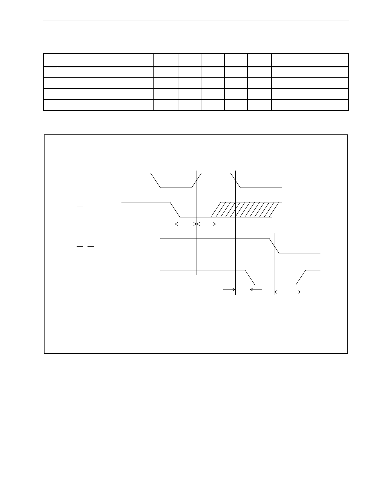
AC Electrical Characteristics†- Frame Pulse, Clock and Change Detect Timing (See Fig.
30) - Voltages are with respect to Ground (V
Characteristics Sym Min Typ
) unless otherwise stated.
SS
‡
Max Units Test Conditions
1 Frame Pulse Setup t
2 Frame Pulse Hold t
3 Change Detect Delay t
4 Change Detect Reset Delay t
† Timing is over recommended temperature and power supply voltages.
‡ Typical figures are at 25°C and are for design aid only; not guaranteed and not subject to production testing.
CK
FP
FPS
FPH
CDD
CDRD
6ns
3ns
38 ns
013ns
t
FPS
t
FPH
DS / CS
CD
* Assumes change in memory contents detected in previous frame
Figure 30 - Frame Pulse and Change Detect Timing
t
CDD*
t
CDRD
2-123
Page 24
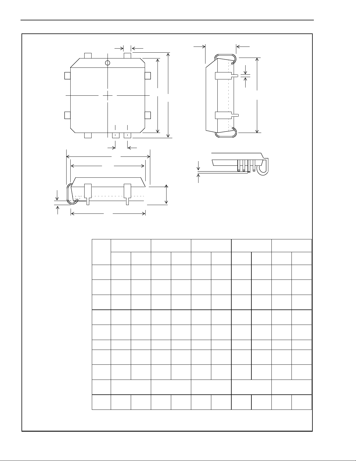
Package Outlines
F
D
1
D
H
E
E
1
e: (lead coplanarity)
A
1
I
E
2
Notes:
1) Not to scale
2) Dimensions in inches
3) (Dimensions in millimeters)
4) For D & E add for allowable Mold Protrusion 0.010"
A
G
D
2
Dim
A
A
D/E
D1/E
D2/E
e
F
G
H
I
20-Pin 28-Pin 44-Pin 68-Pin 84-Pin
Min Max Min Max Min Max Min Max Min Max
0.165
(4.20)
0.090
1
(2.29)
0.385
(9.78)
0.350
1
(8.890)
0.290
2
(7.37)
0.026
(0.661)
0.013
(0.331)
0.020
(0.51)
0.180
(4.57)
0.120
(3.04)
0.395
(10.03)
0.356
(9.042)
0.330
(8.38)
0 0.004 0 0.004 0 0.004 0 0.004 0 0.004
0.032
(0.812)
0.021
(0.533)
0.050 BSC
(1.27 BSC)
0.165
(4.20)
0.090
(2.29)
0.485
(12.32)
0.450
(11.430)
0.390
(9.91)
0.026
(0.661)
0.013
(0.331)
0.050 BSC
(1.27 BSC)
0.020
(0.51)
0.180
(4.57)
0.120
(3.04)
0.495
(12.57)
0.456
(11.582)
0.430
(10.92)
0.032
(0.812)
0.021
(0.533)
0.165
(4.20)
0.090
(2.29)
0.685
(17.40)
0.650
(16.510)
0.590
(14.99)
0.026
(0.661)
0.013
(0.331)
0.050 BSC
(1.27 BSC)
0.020
(0.51)
0.180
(4.57)
0.120
(3.04)
0.695
(17.65)
0.656
(16.662)
0.630
(16.00)
0.032
(0.812)
0.021
(0.533)
0.165
(4.20)
0.090
(2.29)
0.985
(25.02)
0.950
(24.130)
0.890
(22.61)
0.026
(0.661)
0.013
(0.331)
0.050 BSC
(1.27 BSC)
0.020
(0.51)
0.200
(5.08)
0.130
(3.30)
0.995
(25.27)
0.958
(24.333)
0.930
(23.62)
0.032
(0.812)
0.021
(0.533)
(30.10)
(29.210)
(27.69)
(0.661)
(0.331)
0.165
(4.20)
0.090
(2.29)
1.185
1.150
1.090
0.026
0.013
0.050 BSC
(1.27 BSC)
0.020
(0.51)
0.200
(5.08)
0.130
(3.30)
1.195
(30.35)
1.158
(29.413)
1.130
(28.70)
0.032
(0.812)
0.021
(0.533)
General-10
Plastic J-Lead Chip Carrier - P-Suffix
Page 25

http://www.mitelsemi.com
World Headquarters - Canada
Tel: +1 (613) 592 2122
Fax: +1 (613) 592 6909
North America Asia/Pacific Europe, Middle East,
Tel: +1 (770) 486 0194 Tel: +65 333 6193 and Africa (EMEA)
Fax: +1 (770) 631 8213 Fax: +65 333 6192 Tel: +44 (0) 1793 518528
Fax: +44 (0) 1793 518581
Information relating to products and services furnished herein by Mitel Corporation or its subsidiaries (collectively “Mitel”) is believed to be reliable. However, Mitel assumes no
liability for errors that may appear in this publication, or for liability otherwise arising from the application or use of any such information, product or service or for any infringement of
patents or other intellectual property rights owned by third parties which may result from such application or use. Neither the supply of such information or purchase of product or
service conveys any license, either express or implied, under patents or other intellectual property rights owned by Mitel or licensed from third parties by Mitel, whatsoever.
Purchasers of products are also hereby notified that the use of product in certain ways or in combination with Mitel, or non-Mitel furnished goods or services may infringe patents or
other intellectual property rights owned by Mitel.
This publication is issued to provide information only and (unless agreed by Mitel in writing) may not be used, applied or reproduced for any purpose nor form part of any order or
contract nor to be regarded as a representation relating to the products or services concerned. The products, their specifications, services and other information appearing in this
publication are subject to change by Mitel without notice. No warranty or guarantee express or implied is made regarding the capability, performance or suitability of any product or
service. Information concerning possible methods of use is provided as a guide only and does not constitute any guarantee that such methods of use will be satisfactory in a specific
piece of equipment. It is the user’s responsibility to fully determine the performance and suitability of any equipment using such information and to ensure that any publication or
data used is up to date and has not been superseded. Manufacturing does not necessarily include testing of all functions or parameters. These products are not suitable for use in
any medical products whose failure to perform may result in significant injury or death to the user. All products and materials are sold and services provided subject to Mitel’s
conditions of sale which are available on request.
M Mitel (design) and ST-BUS are registered trademarks of MITEL Corporation
Mitel Semiconductor is an ISO 9001 Registered Company
Copyright 1999 MITEL Corporation
All Rights Reserved
Printed in CANADA
TECHNICAL DOCUMENTATION - NOT FOR RESALE
 Loading...