

Page 1
2-101
Features
• Timeslot interchan ge ci rcuit fo r digita l switc h
applicati ons
• 16 bit wide data bus I/O
• 2048 x 16 bi t wide byte ca pac ity
• Dual addres sing ca pab ility; in terna l counte r
and exter nal ad dress bus
• Variable cloc k and f rame ra tes
• Microprocessor in terface
•CMOS
Applications
• Building bl ock for d igital switch ing mat rices
used in PBXs, CO equipment, data switching,
etc.
• Programmable delay lines
Description
The MT9080 is a flexible memory module suitable for
use as a basic building block in the construction of
large digital switching matrices. It can be configured
as either a Data Memory or a Connection Memory.
Interface to the device is via 16 bit wide data and
address busses. The MT9080 can operate with
variabl e cl o c k ra te s up to 16.7 MHz.
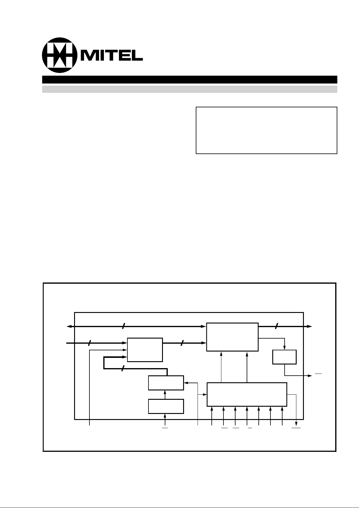
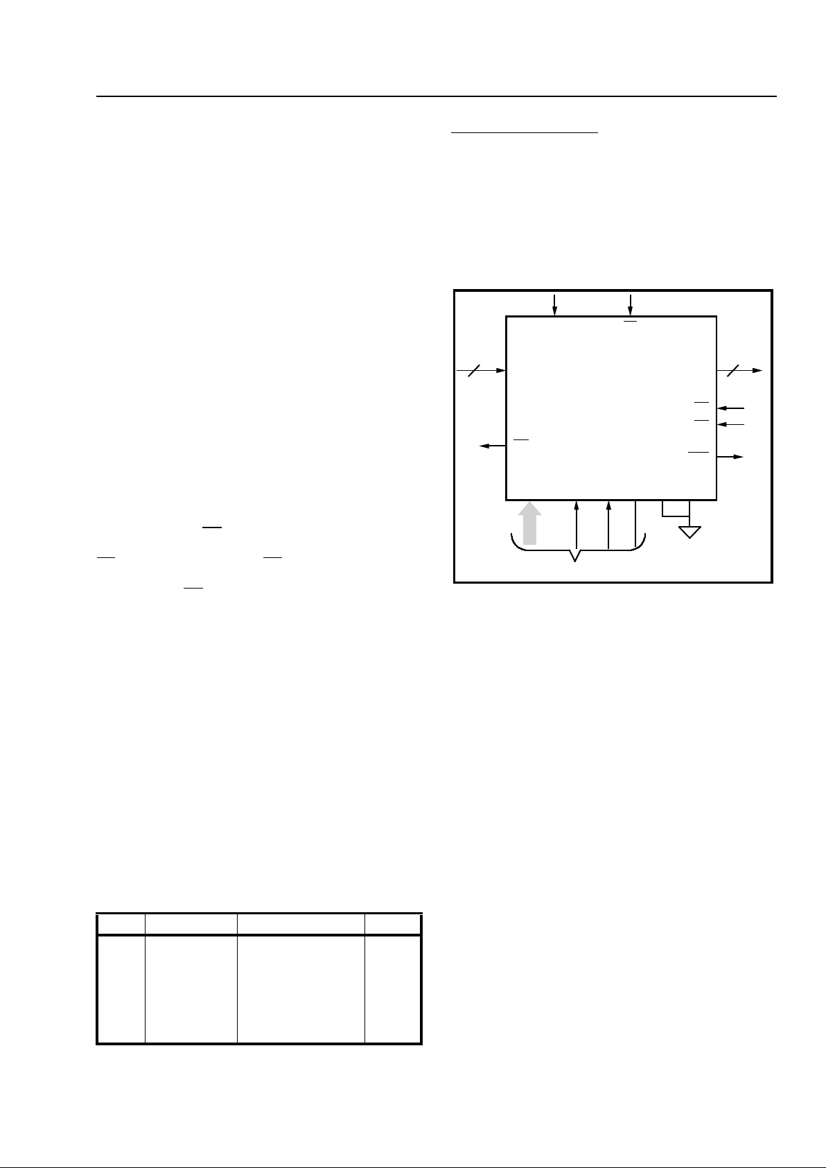
Figure 1 - Functional Block Diagram
D0i/D15i
A0-A15
ME
16
16
16
16
Address
MUX
11 Bit
Counter
Counter
Reset
2048 x 16
Static
Memory
Control Interface
WR
ENABLE
PRECHARGE
D0o/
CD
11
CRC
FP
CK ODE DS CS R/W Mx My Mz DTA
D15o
Ordering Information
MT9080AP 84 Pin PLCC
-40°C to 70°C
ISSUE 3 January 1993
MT9080
SMX - Switch Matrix Module
CMOS
Page 2
MT9080 CMOS
2-102
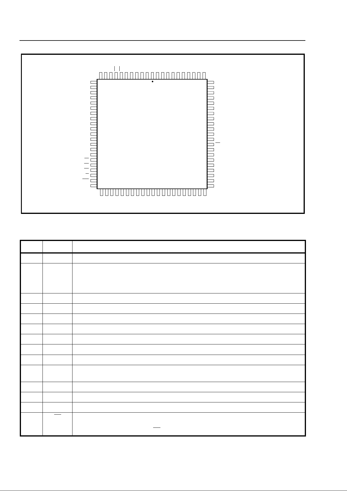
Figure 2 - Pin Connections
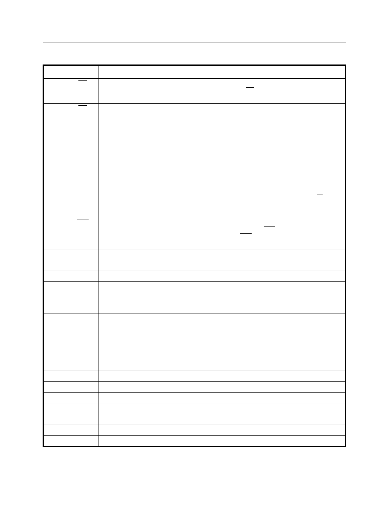
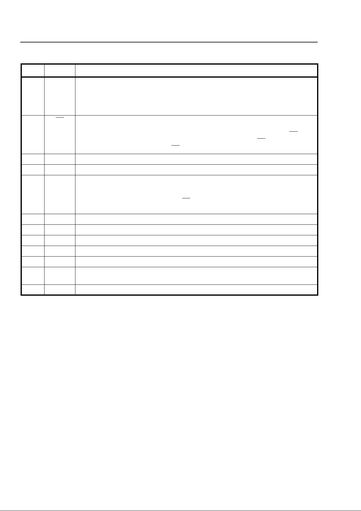
Pin Description
Pin # Name Description
1V
SS
Ground.
2-5 D0i-D3i Input/Micropo rt Data Bus. This is part of a 16 bit data bus. The data bus is bidirectional in
Connect Memory mode where it is typically interfaced to a microprocessor. In all other
modes the data bus is an input. Data to be switched through the device is clocked in at this
port.
6V
SS
Ground.
7-10 D4i-D7i Input/Micropo rt Data Bus. See description for pins 2-5 above.
11 V
SS
Ground.
12-15 D8i-D11i Input/Micr opo rt Data Bus. See description for pins 2-5 above.
16 V
SS
Ground.
17-20 D12i -D15i Input/Microport Data Bus. See description for pins 2-5 above.
21 V
SS
Ground.
22 CK Clock. Master cloc k input which is used to clock data into and out of the device. It also
clocks the internal 11 bit counter.
23 V
DD
+5V supply input .
24 V
SS
Ground.
25,26 IC Internal Con necti on. Should be tied to V
SS
for normal operation.
27 FP
Frame Pulse. An active low signal that serves as a synchronous clear for the int ernal 11 bit
counter in all modes except Shift Register mode. The counter is cleared on a rising edge of
CK. In the Shift Register mode, FP
serves to align channel boundaries.
74
56
58
60
62
64
68
70
72
66
12
28
26
24
22
18
16
14
20
VSS
32
30
54
10
8
6
4
2
84
82
80
78
76
34
36
38
40
42
44
46
48
50
52
NC
ODE
ME
MxMyMz
NC
IC
IC
VSS
VDD
NC
A0A1A2A3A4A5A6
A7
VSS
D7o
D6o
D5o
D4o
VSS
D3o
D2o
D1o
D0o
VSS
CD
A14
A13
A12
A11
A10
A9
A8
D8i
D9i
D10i
D11i
D13i
D14i
D15i
VSS
VSS
IC
CK
VDD
IC
FP
CS
DS
R/W
DTA
NC
VSS
D7i
D6i
D5i
D4i
VSS
D3i
D2i
D1i
VSS
VDD
D15o
D14o
D13o
D12o
VSS
D11o
D10o
D9o
D8o
D0i
84 PIN PLCC
VDD
A15
VSS
D12i
Page 3
CMOS MT9080
2-103
28 CS Chip Select. Active Low input. Selects the device for microport access in connect memory,
data memory, external and shift register modes. Tying CS
high will disable output data
drivers (D0-D15o) in all modes except connect memory and shift register modes.
29 DS
Data Strobe. Active low input. Indicates to the SMX that valid data is present on th e
microport data bus durin g a write operation or that the SMX mu st outp ut data on a read
operation.
In Connect Memory modes, a low level applied to this input during a write operation indicates
to the SMX that valid data is present on the microport data bus. During a read operation the
low going signal indicates to the SMX that it must output data on the micropo rt data bus.
In Data Memory and External modes, when DS
is high, the output data bus D0o-D15o will be
disabled. The input data bus D0i-D15 i is not affected.
The DS
input has no effect on the input and output busses in Counter or Shif t Register
modes.
30 R/W
Read/Write Enable. Data is written into the device when R/W is low and read from it when it
is high. This control input is disabled in data memory and shift registe r modes. It should be
tied to V
SS
or VDD in these modes. In counter and external modes, the state of R/W pin is
clocked in with the rising edge of CK. The actual read or write operation will be implemented
on the next rising clock edge.
31 DTA
Data Transfer Acknowledge. O pen drain out put whi ch is pulled low to acknowled ge
completion of mi croport dat a transf er. On a read of the SMX, DTA
low indicates t hat t he
SMX has put valid data on the data bus. On a write, DTA
low indicates that the SMX has
completed latching the data in.
32 NC No Connection.
33 V
SS
Ground.
34 NC No Connection.
35 ODE Output Data Enable. Control input which enables the output data bus. Pulling this input low
will place the data bus in a high impedance state. The level on this pin is latched by a rising
edge of CK. The output drivers will be enabled or disabled with the rising edge in the next
timeslot (see Fig. 24 for applicable timing in diff erent modes).
36 ME Message Enable. When tied high the data latched in on the address bus is clocked out on
D0o-D15o. When ME is tied low, the contents of the addre ssed mem or y location will be
output on the bus. The level on this pin is latched in with the rising edge of the clock. The
actual mode change is implemented on the rising edge in the next timeslot. Refer to Figures
25 and 26 for more timing information .
37 Mx Mode X. One of three inputs which permit the selection of different operati ng modes for the
device. Refer to Table 1 for description of various modes.
38 My Mode Y. See description for pin 37.
39 M z Mo de Z. See description for pin 37.
40 NC No Connection.
41, 42 IC Internal Connecti on . Leave open for normal ope ratio n.
43 V
SS
Ground.
44 V
DD
Supply Voltage. +5V .
45 NC No Connection.
Pin Description
Pin # Name Description
Page 4
MT9080 CMOS
2-104
46-61 A0-A15 Address Bus. These inputs have three different functions. Inputs A0-A10 are used to
address internal memory locations during read or write operat ions in all m odes except Sh ift
Register mode. In Shift Register mode, the leve ls latched in on A0-A1 0 program the delay
through the device. When the ME pin is tied high, the data latched in on A0-A15 is clocked
out on to the data bus (D0o-D15o).
62 CD
Change Detect. Open drain output which is pulled low when a change in the memory
contents from one frame to the next is detected by a Cyclic Redundancy Check (CRC).
Changes in memory contents resulting from microp rocessor access do not cause CD
to go
low. The output is reset to its normal high impedance state when the DS
input is strobed,
while the device has been selected (CS
is low).
63 V
DD
Supply Voltage. +5V .
64 V
SS
Ground.
65-68 D0o-D3o Output Data Bus. These three state outputs are part of a 16 bit data bus which is used to
clock out data from the device. Data is clocked out with the rising edge of the clock. See
Figures 24 to 26 for timing informa tion. The bus is actively driven when ODE is tied high. It
is disabled when ODE is tied low. Tyin g CS
high will also disable the output data bus in all
modes except Connect Memor y and Shift Register Mode s.
69 V
SS
Ground.
70-73 D4o-D7o Output Data Bus. See description for pins 65-68.
74 V
SS
Ground.
75-78 D8o-D11o Output Data Bus. See description for pins 65-68.
79 V
SS
Ground.
80-83 D12o-D15oOutput Data Bus. See description for pins 65-68.
84 V
DD
Supply Voltage. +5V .
Pin Description
Pin # Name Description
Page 5
CMOS MT9080
2-105
Functional Description
The SMX is a flexible memory module suitable for
use in the construction of timeslot interchange
circuits used in PCM voice or data switches. The
device can be configured as a data memory or a
connection memory.
The SMX has separate 16 bit input and output data
busses. A 16 bit address bus and a full
microprocessor interface is also provided.
Data is clocked into and out of the device with the
signal applied at the CK (clock) input. Depending on
the mode of operation, the memory locations for the
read or write operation can be addressed
sequentially by the internal counter or randomly via
the external address bus. A messaging sub-mode,
which permits the data latched in on the address bus
to be multiplexed on to the output data bus, is also
available (see ME pin description).
The SMX ensures integrity of the stored data by
performing a Cyclic Redundancy Check (CRC) on a
per frame basis. When a change in the memory
contents is detected from one frame to the next, the
Change Detect (CD
) pin is pulled low. The output
will be reset to its normal high impedance state when
DS
input is strobed while CS is low (i.e., while the
device has been selected for microprocessor
access). The CD
output is not pulled low when the
memory contents have been modified by a processor
access to the device.
Modes Of Operation
The SMX can be programmed to operate in one of
eight modes as summarized in Table 1. The different
modes are used to realize specific switch
implementations. For example, to implement a 1024
channel switch, two SMXs are required. One is
operated in Data Memory mode, while the second is
operated in Connect Memory mode. A 2048 channel
switch can be realized using three SMXs. Two of the
devices are operated, alternatively, in Counter and
External modes, the third serves as the Connection
Memory. A detailed description of the
implementation is presented in the Applications
section of this data sheet. An outline of the device
functionality in each mode is presented below.
Table 1. SMX Mode s of Oper ation
Mode MXMYM
Z
Name Abbr.
1
2
3
4
5
6
7
8
0
0
0
0
1
1
1
1
0
0
1
1
0
0
1
1
0
1
0
1
0
1
0
1
Data Memory - 1
Data Memory - 2
Connect Memory - 1
Connect Memory - 2
Counter Mode
External Mode
Shift Register Mode
Data Memory - 3
DM-1
DM-2
CM-1
CM-2
CNT
EXT
SR
DM-3
Data Memory Mode-1
Data Memory Mode-1 is designed for use in the
construction of a 1024 Channel Switch Matrix. Data
on the D0-D15 input bus is clocked into the S MX and
stored in memory locations addressed by the internal
11 bit counter. Data is clocked out according to the
addresses asserted on the address bus. The pin
configuration of the device in this mode is illustrated
in Fig .3
Fig. 3 - Data Memory Modes 1 and 2 Pinout
The timing for the read and write operation is
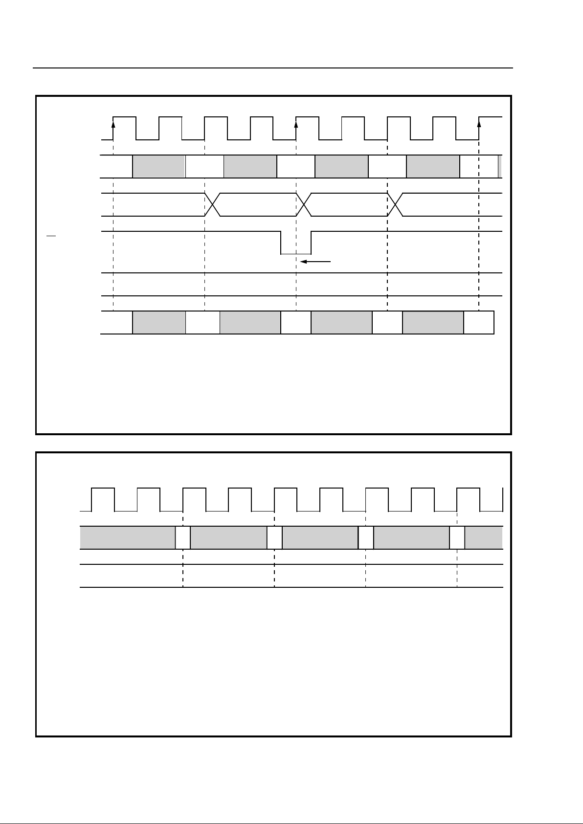
illustrated in Fig. 4. The first half of each clock period
is used for precharging the internal bus. Data is
latched in and out of the device with rising edge of
the CK clock. Correct operation of the device in this
mode requires 2048 clock cycles in a single frame
defined by the frame pulse. Consequently, for
switching of 64 kbit/s PCM voice channels, the clock
frequency must be 16.384 Mbit/s with a frame rate of
8 kHz.
The address supplied on the address bus is latched
in with the first positive clock edge in a channel
timeslot. The contents of the memory location
addressed will be clocked out on D0-D15o with the
first positive clock edge in the next timeslot (see Fig.
4).
In Data Memory Mode-1, the delay through the
switch depends on the number of channel timeslots
between the input c hannel and the output channel. If
the time difference between the input channel and
output channel is less than two channels, data
clocked into the device in the current frame will be
clocked out in the next frame. If the difference is
greater than or equal to two channels, data will be
clocked out in the same frame. This concept is
further illustrated in Fig. 5.
Data
Input
Data
Output
16
FP
D0i-D15
i
CD
A0-A15 ME ODE ZYZ
D0
o
-D15
o
CS
DS
DTA
16
MODE
CK
From Control Interface
Page 6
MT9080 CMOS
2-106
Figure 4 - Data Memory Mode Functional Timing
Figure 5 - Throughput Delay in Data Memory Mode-1
CK
External
Address
Bus A0-A15
Data Output
D0-D15o
FP
Address
generated by
Internal 11
Bit Counter
Data Input
D0-D15i
CH X CH Y CH Z
1022
1023
0
1
2101023
Counter Reset
CH X CH Y CH Z
PWP R
➀②
P = Precharge
R = Read Memory
W = Write Memory
Data is clocked out of the memory location addressed by external address bus. The address is latched in with CK edge
marked ➀. Data is clocked out with CK edge marked ②.
Data is latched into the device with the last rising edge of CK in the timeslot (e.g., edge ➂ in diagram). It is stored in the
➂➃
memory location address by the internal 11 bit counter with the next rising clock edge (edge ➃ in diagram).
CK
PW R
➀②
P
1 4
12345
23
P = Precharge
R = Read Memory
W = Write Memory
Data on the input bus of the SMX is latched into the device with last rising edge of the clock within a timeslot. It is
Data is clocked out of the memory location and latched onto the output data bus with first positive clock edge in the
Input
Data
Output
Timeslots
written into the internal memory with the following positive edge.
timeslot.
Switching channel 1 to channel 1 or channel 2 will result in one frame delay. Note that channel 2 is clocked out by CK
edge labelled ➀ while channel 1 is written into the memory with edge ②. However, if channel 1 is switched to channel
3, there will be only one channel delay.
Page 7
CMOS MT9080
2-107
This mode provides minimum delay through the SMX
for any switching configuration.
Data Memory Mode-2
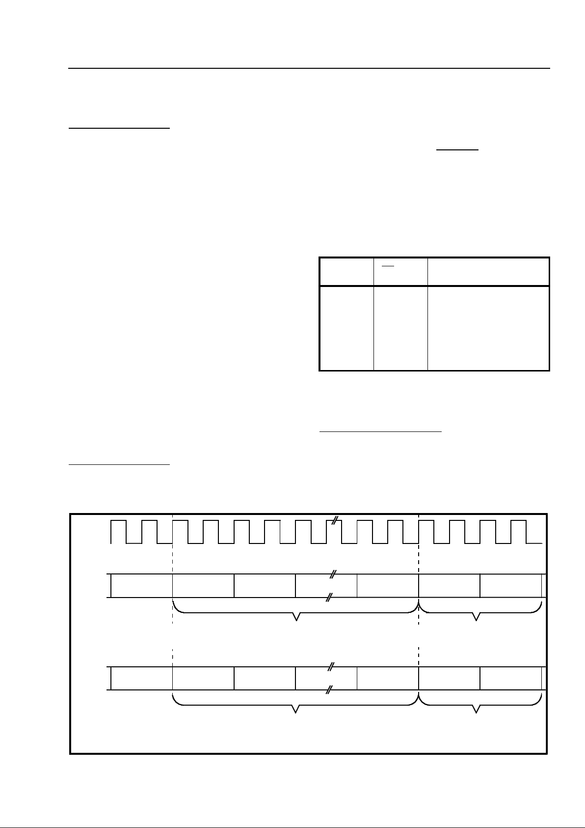
Data Memory Mode-2 is designed for use in
constructing a 1024 by 1024 channel double
buffered switch. This mode is similar in most
respects to Data Memory Mode-1. The double
buffering is achieved by dividing the internal 2048
memory into two equal blocks. In a single frame,
data is written into the first block and read from the
second. In the next frame, the data will be written
into the second and read from the first (see Figure
6). Frame sequence integrity of the data will be
maintained for all switching configurations if the
output frame is delayed by one channel with respect
to the input frame. In this case, data clocked into the
device during any of the channels in the current
frame will be clocked out in the next frame. However,
if the input and output frames are aligned, then data
switched from any input channel to output channels
0 or 1 will be clocked out one frame after the next consequently frame sequence integrity is not
maintained for channels 0 or 1. Frame sequence
integrity will be maintained for data switched to any
of the other output channels. (See SMX/PAC
Application Note, MSAN- 13 5 , f or mo r e info r m ati o n. )
It is possible to switch between Data Memory
Mode-1 and Mode-2 on a per timeslot basis.
Data Memory Mode-3
This mode is similar to Data Memory Mode-1.
However, there is no restriction on the minimum
acceptable clock frequency or frame rate. In this
mode, the size of the switching matrix depends on
the clock and frame rates provided as per the
following relationship:
where S is the number of channels in the switching
matrix F
FP
is the frame pulse frequency in Hz, and
F
CK
is the clock frequency in Hz. The following table
shows how the size of a switching matrix can be
varied by selecting a suitable combination of clock
and frame rates.
It is not possible to switch between Data Memory
Mode-3 and other modes on per-timeslot basis.
Connect Memory Mode -1
In Connect Memory Mode-1, the input data bus is
bidirectional. Internal memory locations can be
randomly accessed via the microprocessor bus. The
pinout of the device in this mode is illustrated in
Figure 7.
CK (kHz) FP
(kHz)
Number of channels in
the switching m atrix
16.384
16.384
16.384
12.288
12.288
8.192
8.192
4
8
16
4
8
4
8
2,048
1,024
512
1,536
768
1,024
512
S
=
F
CK
2 X F
FP
Figur e 6 - Da ta M em or y Mo de -2 F unc ti on al Tim ing
CK
Data
Input
Data
Output
FRAME 0
FRA ME 1
FRAME 2
FRA ME 1
FRAME 2
1023
0
1
102301 01
0
1
Written to Block 0 Written to Block 1
Read from Block 1 Read from Block 0
FRAME 0
Written to
Block 1
Read from
Block 0
1023
1023
Note: No input and output channel alignment is implied in the example shown above. It is assumed that the frame pulse for the
connection memory used to generate adresses for the read operation has a specific phase relationship with respect to the Data
Memory frame pulse.
Page 8
MT9080 CMOS
2-108
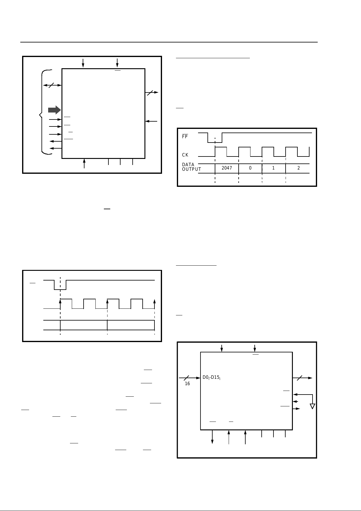
Fig. 7 - Connect Memory Modes Pinout
Data is clocked out on D0
o
-D15o from memory
locations addressed sequentially by the internal
counter. This counter is incremented every second
clock period and is reset with FP
. The frequency of
the clock signal used should be twice the data rate.
A timing diagram showing the relationship between
the data output and the clock signal is presented in
Fig. 8. With a clock rate of 16.384 MHz, the
maximum number of addresses that can be
generated in an 8 kHz frame period is 1024.
Fig. 8 - Connect Memory Mode-1 Functional
Timing
Microprocessor access timing is shown in Figures 28
and 29. During a microprocessor read cycle, DS
low
indicates to the SMX that the processor is ready to
receive data. The SMX responds by pulling DTA
low
when there is valid data present on the bus. The
processor latches the data in and sets DS
high. The
SMX completes the bus cycle by disabling the DTA
.
DS
should be kept low until after DTA is issued by
the SMX. CS
, R/W and the address lines should
also be asserted for the duration of the access. A
MPU write cycle is similar to the read cycle. Data will
be latched into the device approximately three clock
(CK) cycles after DS
goes low. When the device
has latched the data in, it will pull D TA
low. DS can
subsequently be set high.
16
CK
D0-D15
16
ODE
ME Z Y X
MODE
CD
DTA
CS
DS
R/W
A0-A15
D0
o
-D15
o
FP
0/1 1 0
Microprocessor
Interface
FP
CK
Data
Out
1023 0
Connect Memory Mode-2
Connect Memory Mode-2 is designed specifically for
2048 channel switching applications. Data is clocked
out on D0
o
-D15o with every rising clock edge from
memory locations addressed sequentially by the
internal counter (see Figure 9). This counter is
incremented with each clock period and is reset with
FP
or when a count of 2047 is reached.
Fig. 9 - Connect Memory Mode-2 Funct ional
Timing
The clock frequency should be 16.384 MHz for a
connection memory designed to support a 2048
channel switch.
Microprocessor access is similar to Connect Memory
Mode-1.
Counter Mode
This mode is designed for 2048 channel switching
applications. In the counter mode all read and write
addresses are generated sequentially by the internal
11 bit counter. The 11 bit counter is incremented
with each clock pulse. It will wrap around when it
reaches a count of binary 2047 or when it is reset by
FP
. The active input/output pins in this mode are
illustrated in Fig. 10.
Fig. 10 - Counter Mode Pinout
A
AAA
A
A
A
A
A
A
FP
CK
DATA
OUTPUT
2047 0 1 2
16
D0
i
-D15
i
CK FP
D0o-D15
o
CS
ODE
DTA
CD R/W ME XYZ
16
All other inputs should
be tied Low
100
Page 9
CMOS MT9080
2-109
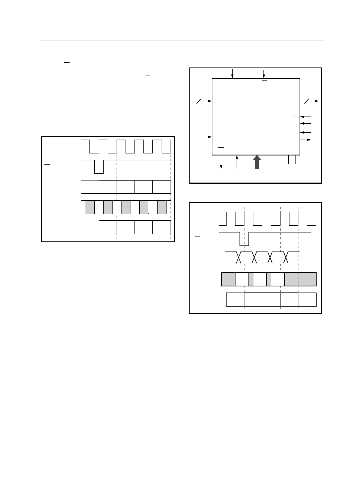
The device can perform either a read or a write,
depending on the level asserted at the R/W
pin.
When R/W
is high, the contents of the memory
addressed by the internal counter will be clocked out
on to the output data bus. Setting R/W
low will
enable data on the input data bus to be written into
the device. During a write operation, the output bus
is actively driven by the data latched out in the
previous read operation.
Data is clocked in or out of the device on the positive
edge of the clock. See Fig. 11.
Fig. 11 - Counter Mode Functional Timing
External Mode
The external mode, which is designed for use in
2048 switching applications, permits random access
to the memory both for input and output operations.
The pinout for external mode is shown in Fig. 12.
The address asserted on the external address bus is
used to specify the memory location to be accessed
for the read or write operation. The level asser t ed on
R/W
during a specific clock period determines
whether the addressed memory is written to or read
from. During a write operation, the output data bus
is actively driven with data latched out in the
previous read operation.
Data is clocked into or out of the device on the
positive edges of the clock as shown in Fig. 13.
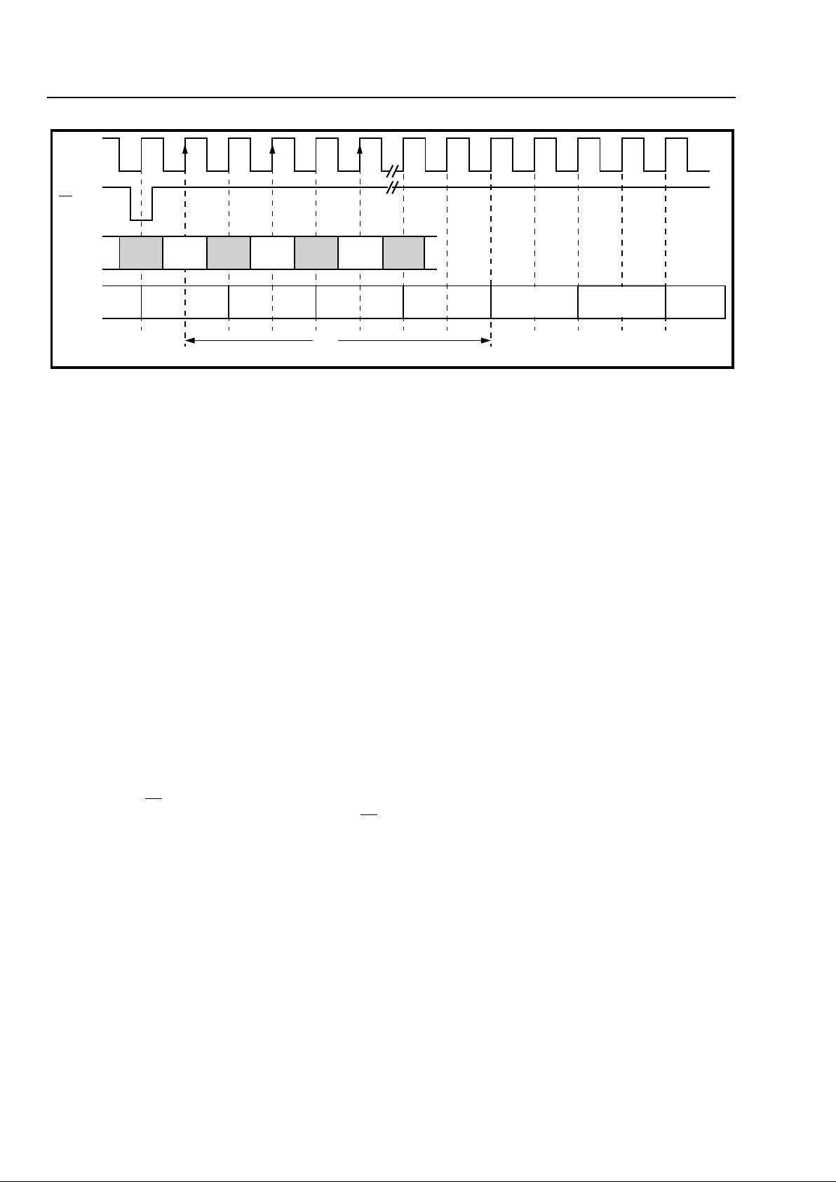
Shift Regis t er Mode
In this mode, data clocked into the SMX is delayed
by a number of clock cycles before being clocked out
of the device. The delay introduced (in number of
clock cycles) is equal t o two times the binary value of
the address latched into the device plus 2. For
CK
FP
Internal
Counter
Data Clocked Out
(R/W
High)
Data Clocked In
(R/W
LOW)
2047 0 1 2 3
012
2047 0 1 2
3
example, if the address asserted is Hex 02, the delay
through the switch is equal to six clock cycles.
Figure 12 - External Mode Pinout
Figure 13 - External Mode Functional Timing
Maximum permissible delay is equal to 4096 clock
cycles.
The pertinent timing parameters are illustr a ted in Fig.
14. Data is clocked in and out of the device with
rising edge of the clock.
The address is latched in with the negative edge of
DS
while the CS is low.
16
D0
i
-D15
i
CK FP
D0o-D15
o
CS
DS
CD
R/W
A0-A11
XYZ
16
ODE
DTA
ME
101
All other inputs should
be tied Lo w
CK
FP
ADDR
Data In
(R/W
Low)
Data Out
(R/W
High)
CH X CH Y
CH Z
XYZ
CH X CH Y CH Z
Page 10
MT9080 CMOS
2-110
Figure 14 - Shift Register Mode Data Input/Output Timing
CH X CH Y CH Z
CH X CH Y CH Z
t
d
td = (Address x 2) + 2 Clock Cycles
CK
FP
Data
In
Data
Out
Applications
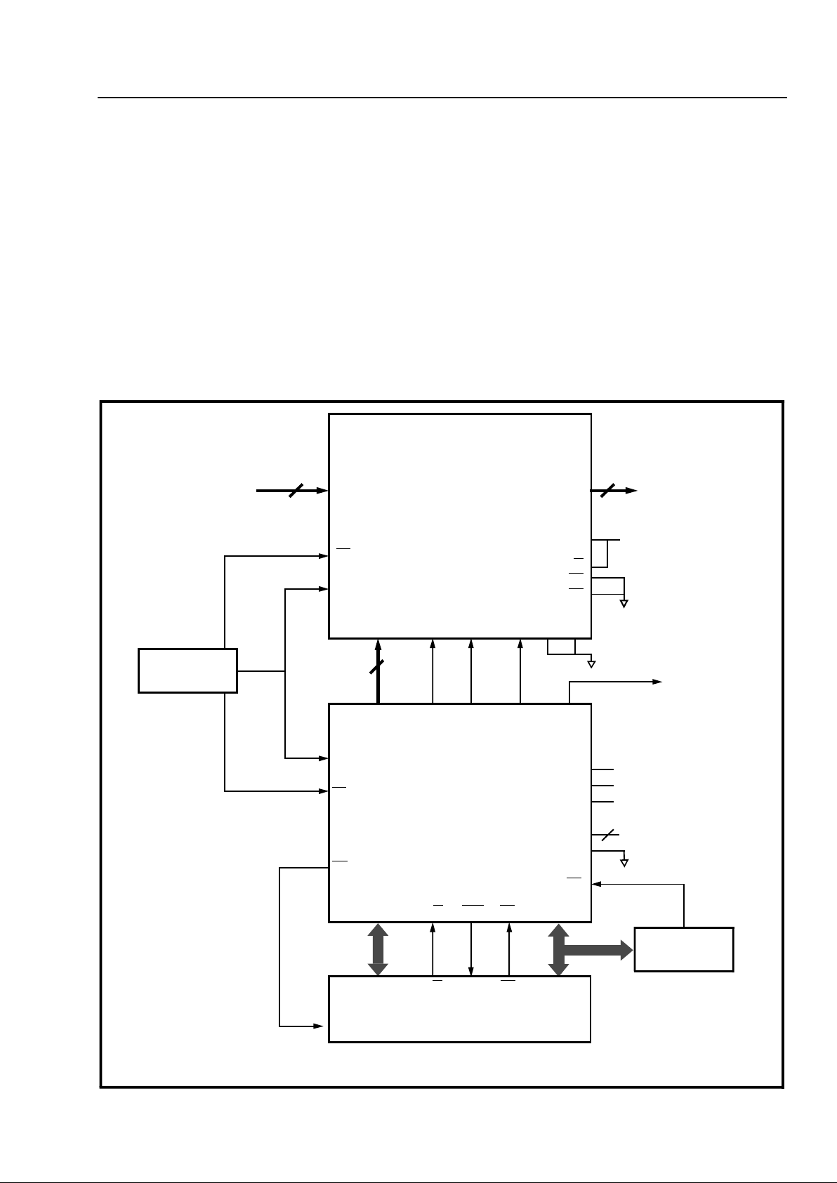
1024 Chann el Sw itch M atrix
A 1024 channel, non-blocking, timeslot interchange
switch can be constructed using two SMX devices
(refer to Figure 15). One SMX is operated in the
Data Memory mode, while the second device is
operated in Connect Memory Mode-1.
Data to be switc hed i s clo cked i nto th e d ata m emo ry
via the 16 bit input data bus and stored sequentially
in memory locations addressed by the internal 11 bit
counter. The data is read out of the Data Memory
(SMX#1) according to the external address supplied
by the Connection Memory (SMX#2). The
Connection memory clocks out contents of the
memory according to the addresses supplied by the
internal c o un te r.
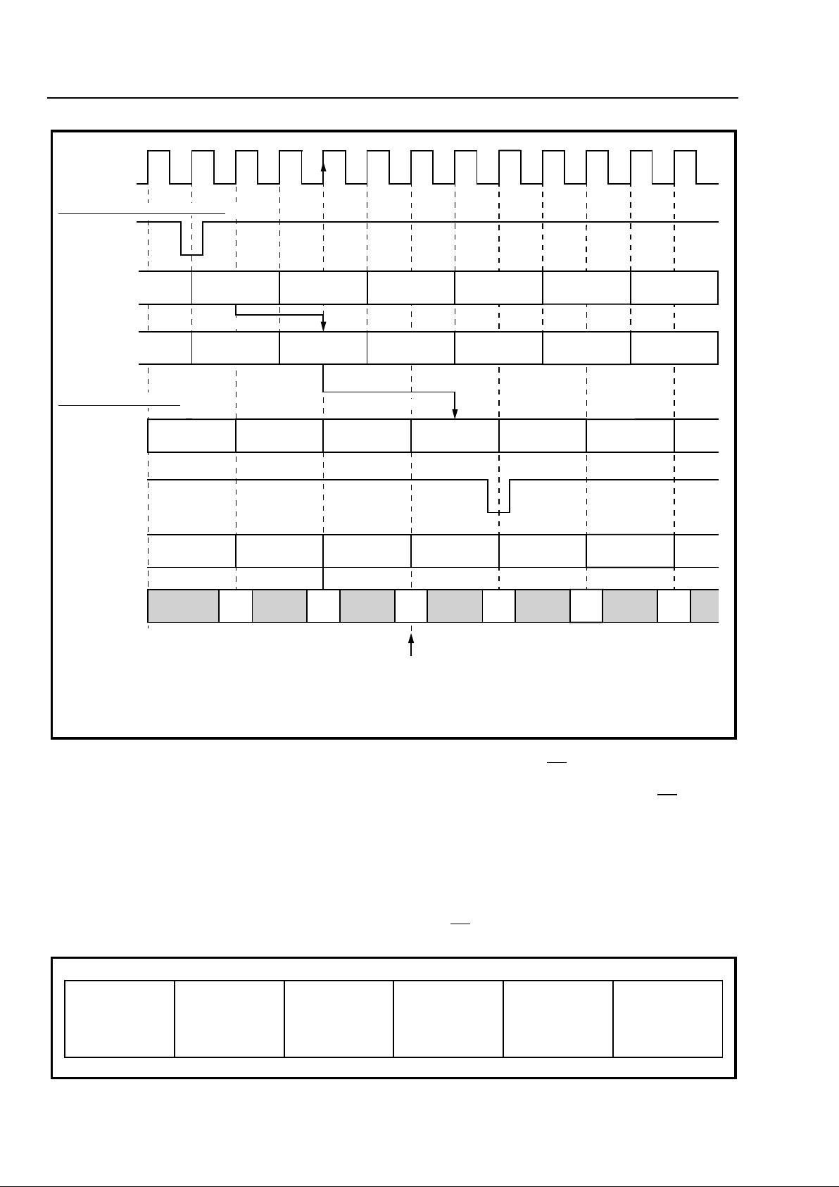
The clock applied at the CK input of both the devices
has a frequency of 16.384 MHz. There are two clock
periods in each channel timeslot (see Figure 16). A
framing signal (FP
) with a frequency of 8 kHz is used
to delinate frames with 1024 channels each. The FP
input to the Data Memory is delayed by seven clock
periods from the Connection Memory frame pulse.
This phase delay synchronizes the internal counters
of the two SMXs such that the Connection Memory
clocks out addresses one channel ahead of the
affected timels ot .
Using the connections illustrated in Figure 15, the
Data Memory address and control functions can be
mapped onto specific bits of the Connect Memory to
form a 16 bit control word, as shown in Figure 17.
The 16 bit control word is written into the Connection
Memory by the processor. Subsequently, when the
memory location is addressed by the internal
counter, this word will be clocked out of the memo ry
on to the data bus (D0
o
-D15o).
The output on the Connect Memory data bus
(D0o-D9o) is used to specify the Data Memory
location to be read out during any particular timeslot.
The Connection Memory is programmed in a manner
that permits specific addresses to be output in
certain timeslots. The Data Memor y will clock out
data from internal memory locations according to the
address asserted on its address bus. As mentioned
earlier, this address is latched into Data Memory with
a positive edge of the clock. The contents of the
appropriate addressed memory location will be
clocked out of the device at the beginning of the next
channel tim eslo t.
Connection Memory bit 10 controls the level on the
ODE input. The ODE pin is used to enable the
output drivers of the Data M emory. The capability to
selectively enable or disable the output drivers
during specific channel timeslots is required when
constructing larger switches using the 1024 channel
switch as a building block.
The Message Enable (ME) input of the Data Memory
is controlled by D11. Setting this particular bit high
will result in the data latched into the address bus
being clocked out on to the Data Memory output bus.
Note that only 10 of the 16 address inputs are
actually connected to the data bus of the Connection
Memory. Consequently, only 10 of the 16 data output
bits on the Data Memory can be dynamically
controlled through the Connection Memory. In other
applications, all 16 of the address bits may be
connected to the data output bus of the Connection
Memory.
The mode of operation of the Data Memory can be
changed from Data Memory Mode-1 to Data Memory
Mode-2 by setting or resetting D12 in the connection
Page 11
CMOS MT9080
2-111
memory. The delay through the matrix can be
optimized for specific applications by selectively
enabling one of the two modes. Data Memory-1
(DM-1) is designed for voice switching applications
where it is generally desirable to minimize delay
through the switch. As mentioned earlier in the
DM-1 description, the delay through the switch
depends upon the difference between the input
channel timeslot and the output channel timeslot.
Consecutive output channels switched from
non-contiguous input channels will not always
originate from the same input frame. For example, if
channels 3, 6 and 8 are to be switched to channels
5, 6 and 7; output channel 5 will contain data input in
the current frame, while channels 6 and 7 will contain
data clocked in one frame earlier. Data Memory-2
(DM-2) is designed for data switching applications
where concatenation of a number of channels is
often necessary. Data clocked out of the device will
originate from the previous frame, regardless of the
input/output time difference. There is one exception,
when channel 1023 is switched to channel 0, the
contents of Channel 0 will not originate from the
previous frame but rather from the frame before it.
The capability to selectively change between DM-1
and DM-2 allows a single switch to handle both voice
and data effectively.
External bus drivers can be controlled with D13 of
the Connection Memory data bus. Th is bit will be
output along with the remaining bits one channel
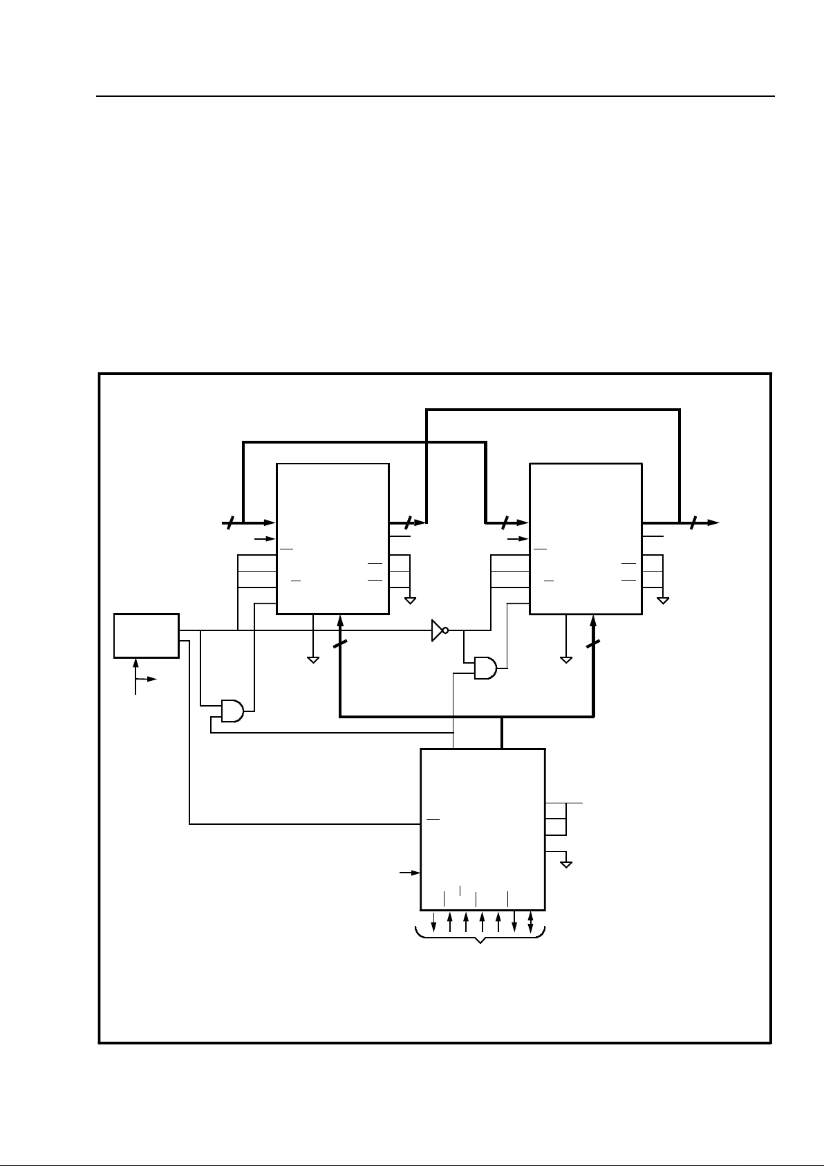
Figure 15 - 10 24 C hanne l Swit ch Matr ix
Parallel Input Data
Parallel Output Data
16
16
D0
i
-D15
i
D0o-D15
o
SMX #1
DM-1/2
DATA
MEMORY
A10-A15
R/W
CS
DS
FP
CK
A0-A9 ODE ME Z Y X
MODE
10
+5
External
Tristate
Control
Timing
Generator
FP#1
CK
FP#2
D0
o
-D9oD10oD11oD12oD13
o
X
Y
Z
MODE
A11-A15
A10
CS
CK
FP
CD
D0-D15 R/W DTA DS A0-A9
SMX #2
CM-1
CONNECTION
MEMORY
0
1
0
+5
Address
Decode
D0-D15 R/W
HALT DS
IRQ
16-BIT MPU
Note: All other inputs not shown in this diagram should be connected to GND.
Page 12
MT9080 CMOS
2-112
Figure 16 - 1024 Channel Switch Timing
CK
FP #2
Internal
Counter
(Read
Address)
Data Output
D0o-D15o
DATA MEMORY TIMING
Data Output
D0o-D15o
FP #1
Internal Counter
(Write Address)
Data In
D0i-D15i
CONNECTION MEMORY TIMING
➀②➂➃
1023012345
1022 1023 0 1 2 3 4
1021 1022 1023 0 1 2 3
1021 1022 1023 0 1 2
1021 1022 1023 0 1 2
addresses
SMX #1 Data Input/Output Frame Boundary
Note 1: Address is latch ed into the Data Memo ry by the first positi ve clock e dge in a timeslo t (ed ge ➀ for Ch. 0). Data will be
clocked out by the first positive clock edge in the next timeslot (edge ② for Ch. 0).
Note 2: Data is latched into the Data Memory by the first rising edge in a timeslot (edge ➂ for Ch. 0) and is written into the
memory location addressed by the internal counter with the next rising edge (edge ➃ for Ch. 0).
addresses
ahead of time; i.e., one channel before the
addressed data is clocked out of the Data Memory. It
may be necessary to provide an external bus enable
one channel ahead of time in applications where
precharging of the external data bus is required. In
other applications where no precharge is required,
control bit from the next channel may be used in
order to ensure that the external bus is enabled at
the same time as the channel is being clocked out of
the device.
The Change Detect (CD) output of the Connection
Memory is used to interrupt the MPU. As mentioned
in the Pin and Functional descriptions, CD
goes low
when the internal CRC performed by the device
indicates a change in memory contents. This feature
is particularly useful in switching applications where
the Connection Memory is configured once and is
not modified for long periods of time, e.g., in network
digital access crossconnect systems. Any
inadvertent corruption of the memory contents will
cause CD
to interrupt the processor.
Figure 17 - Mapping of Address and Control Signals onto Connect Memory Data Bits
D15 - D14
Unused
D13
External
Driver
Enable
D12
DM-1 or
DM-2
Select
D11
Message
Enable
D10
ODE
Control
D9 - D0
Source
Channel
Address
Page 13
CMOS MT9080
2-113
Switching any input channel to an output channel
timeslot is possible by merely writing the address of
the input ch a nne l i n th e C o n nec ti on Memory lo cati o n
corresponding to the output channel timeslot. For
example, to switch channel 1 to output channel 5
and enable output drivers during channel 5, the
Connection Memory location corresponding to
channel 5 should be loaded with Hex 2001. This
word will be clocked out of the Connection Memory
during timeslot 4 and will cause the Data Memory to
clock out contents of the memory corresponding to
channel 1 during the channel 5 timeslot. The 16 bit
word clocked out by the Connection Memory will also
enable Data Memory output drivers, and, external
drivers.
2048 Channel Switch Matrix
A 2048 channel, double buffered timeslot
interchange switch can be constructed with three
SMXs as shown in Figure 18. SMX#1 and SMX#2
are used to store data and switch it in time, while the
third SMX functions as a Connection Memory.
SMX#1 and 2 are operated in the Counter Mode and
External Mode alternatively in consecutive frames.
In any specific frame, one of the two is in Counter
mode while the other is in External mode. The
functions are reversed in the successive frame. The
SMX in counter mode is programmed to write data
Figure 18 - 2048 Channel Timeslot Interchange Circuit
CM-2
SMX #3
D11 D0o-D10o
ODE
Mz
My
Mx
FP
CK
+5
C16
MPU Interface
CONNECTION
MEMORY
U2
U1
11
11
+5
161616
C16
+5
C16
C16
16
D0-D15i
CK
FP
Mz
R/W
ODE
A0-A10
ME
D0-D15o
Mx
My
CS
DS
CNT/EXT
SMX #1
D0-D15i
CK
FP
Mz
R/W
ODE
A0-A10
ME
D0-D15o
Mx
My
CS
DS
CNT/EXT
SMX #2
Data
Output
DATA
MEMORY
DATA
MEMORY
Timing
Generator
DFP
CFP
16.384 MHz
Notes:
1) U1 and U2 are required if the data output bus is to be enabled/disabled via the microprocessor interface.
2) All inputs not shown should be connected to Ground (V
SS
).
DTADSR/W
CS
A0-A15CDD0-D15
Page 14
MT9080 CMOS
2-114
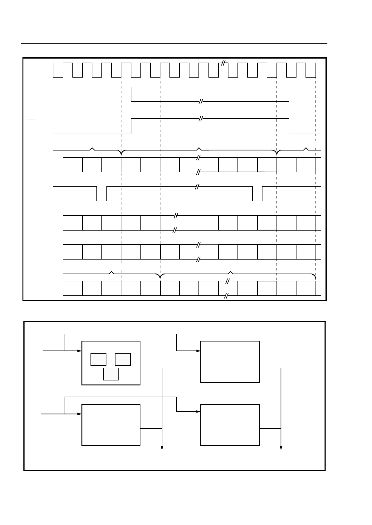
Figure 19 - 2048 Channel Switch Timing
Figure 20 - Extended Switching Matrix
CK
DFP
DFP
(SMX #2)
Data In
(SMX1/2)
CFP
(SMX #3)
SMX #3
Int. Counter
SMX #3
D0o-D10o
Data Out
(SMX 1/2)
(SMX #1)
2044 2045 2046 2047 0 1 2 2044 2045 2046 2047
0122045 2046 2047 0 1 2045 2046 2047
01 2
2045
2046 2047 012
2045
2046 2047
012046 20472046 2047 0 1 2
Written to SMX #2 Written to SMX #1
Read from SMX #1
Read from SMX #2
Written from SMX #2
Data
In
Data
In
LARGE MATRIX 1
DM
DM
CM
ODE
CH 2,049-4,096
CH 1-2,048
CH 2,049-4,096
CH 1-2,048
LARGE MATRIX 3
ODE
LARGE MATRIX 2
ODE
LARGE MATRIX 4
ODE
Data Out Data Out
Page 15
CMOS MT9080
2-115
into its memories addressed by the internal counter.
The SMX in the external mode reads data out from
memory locations addressed by the Connection
memory. In this manner, incoming data is continually
written into one memory block while it is being read
out of the other block. The device in counter mode
has its output drivers disabled.
This configuration results in a maximum throughput
delay of two fram es. Data clo cked into the devic e in
the current frame is clocked out in the next frame.
The appropriate timing parameters are illustrated in
Figure 19. The clock signal applied to all three
SMXs has the same frequency.
SMX#3 is operated in Connect Memory Mode-2. In
this mode, data is clocked out of the device at the
same rate as th e c loc k, i.e., at 16.384 M b ps .
Extended Switching Matrix
Larger extended switch matrices can be created
using the 1024/2048 channel switch as a building
block. As shown in Figure 20, a 4096 channel matrix
would require four smaller 2048 channel building
blocks.
Construction of matrices larger than 4K may require
external drivers to accommodate the greater
capacitive loading on the outputs.
Using the SMX for Me ssag ing
In some system architectures the PCM voice signals
and system status information is transmitted and
received over a common backplane. To facilitate
microprocessor access to the backplane, the SMX
can be used to read incoming data or write to a
channel on the output data bus.
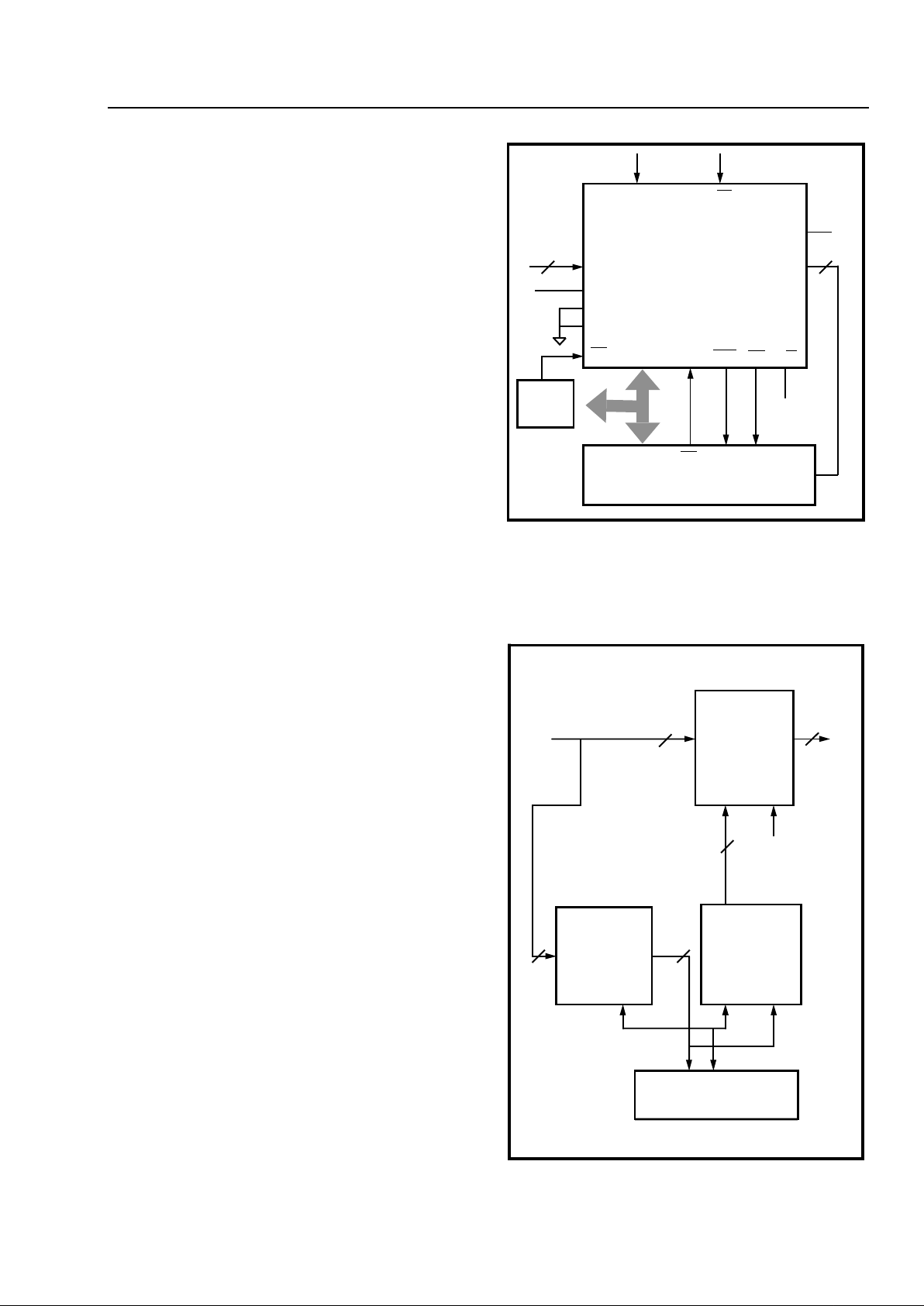
Data clocked into the SMX can be read from the
device by a microprocessor interfaced to the output
data bus and the address bus (see Figure 21). Data
can be written to a specific timeslot on the output
data bus directly by the microprocessor using the
messaging feature (enabled by tying the ME pin
high) .
A 1024 Switch Matrix with messaging capability can
be constructed with three SMXs as shown in Figure
22. The first SMX is used for performing the actual
switching function. The second SMX is configured
as the connection memory. As discussed in the
1024 switch application, by enabling the messaging
feature, data clocked out of the connection memory
and latched into the data memory address bus will
be clocked out on to the data bus directly. Incoming
data is read by the microprocessor using the third
Figure 21 - Readi n g th e Data Me m o ry with a
Micropr ocessor
SMX. The data output bus of the third SMX is
connected to th e da ta b u s of the MPU.
Figure 22 - A 1024 Ch ann el Swit ch Ma trix with
Message Ca pab ility
CK FP
D0-D15i
Z
Y
X
CS
A0-A11
DS DTA
CD R/W
D0-D15o
ODE
ADDRESS DS
HALT IRQ
D0-D15
M P U
Address
Decode
16
16
+5V
+5V
DM-1/DM-2
SMX #1
DATA MEMORY
SMX #2
CONNECTION
MEMORY
SMX #3
MESSAGING
DM-1/2
DM-1 CM-1/2
MPU
Data in
Data out
16
16
ADDR ME
+5V
16
D0
i
-
D15
i
ADDR
D0
o
-
D15
o
ADDR DATA
ADDRDATA
16
16
Page 16
MT9080 CMOS
2-116
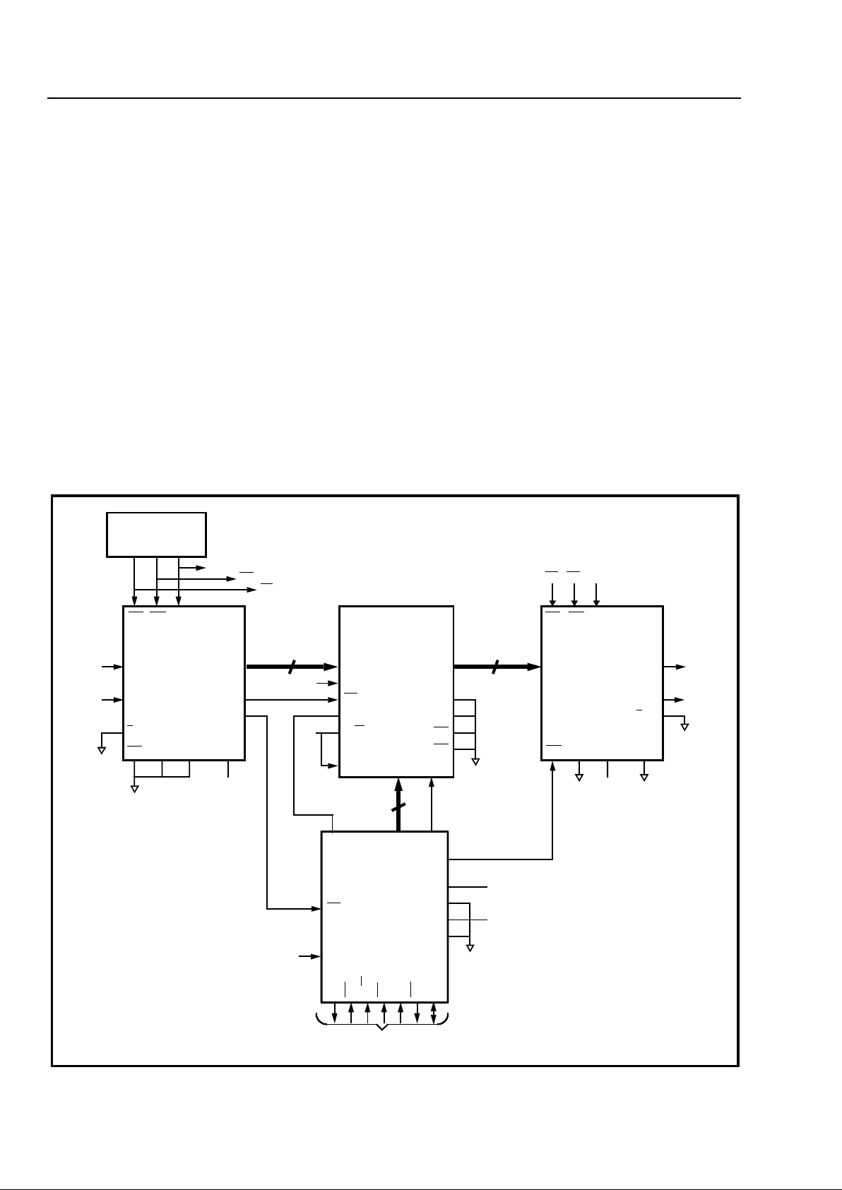
Parallel-to-Serial Conversion
The SMX can be used in systems which employ
serial architectures by converting the parallel I/O into
a serial format. The Mitel MT9085 Parallel Access
Circuit (PAC) is designed to interface to the parallel
busses of the SMX. A single PAC can convert the
output of a1024 channel switch into 2.048 Mbit/s or
4.096 Mbit/s serial format. A second PAC can be
configured to implement serial to parallel conversion
(see Figure 23).
The PAC generates all framing signals required to
implement a 1024 or 2048 channel matrix. Refer to
the MT9085 data sheet for more information on
operation of the PAC.
For more information, see Mitel’s Application Note
MSAN-135
“Design of Large Digital Switching
Matrices using the SMX/PAC“
.
Figure 23 - 1024 Channel Serial Switch Matrix Using the PAC and SMX
Timing
Source
C4i
C16i
S0
S31
•
•
•
•
2
/4S
OE
CKD
MCA
MCB
P0-P7
DFPo
CFPo
PAC
S/P
F0i
•
•
•
•
S0
S31
C16
C4
F0
8
C16
+5
+5
D0-D7i
CK
FP
Mz
R/W
ODE
A0-A9 ME
D0-D7o
Mx
My
CS
DS
8
SMX #1
DM - 1/2
F0
C4 C16
F0i
C4i C16i
P0-P7
OE
CKD MCA
MCB
2
/4S
+5
•
•
•
•
S0
S31
•
•
•
•
S0
S31
PAC
P/S
SMX #2
CM - 1
D12 D0-D9 D11
D10
ODE
Mx
My
Mz
FP
CK
+5
+5
C16
MPU Interface
NOTE: Connect all inputs not shown to V
SS
10
CONNECTION
MEMORY
DATA
MEMORY
DTADSR/W
CS
A0-A15CDD0-D15
Page 17
CMOS MT9080
2-117
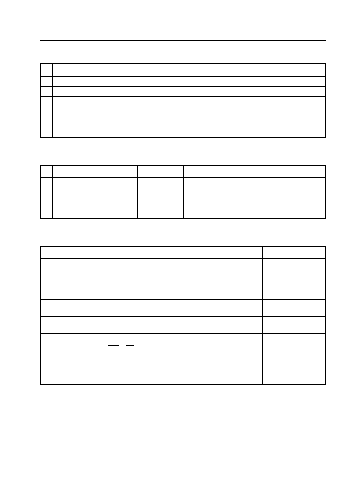
* Exceeding these values may cause perm anen t damage . Function al operati on under the se conditi ons is not impl ied.
‡ Typical figures are at 25°C and are for design aid only: not guaranteed and not subject to producti on testing.
‡ Typical figures are at 25°C and are for design aid only: not guaranteed and not subject to producti on testing.
Absolute Maximum Rating s*
Parameter Symbol Min Max Units
1 Supply Voltage V
DD-VSS
V
DD
-0.3 7 V
2 All Input Voltages V
i
VSS-0.3 V
DD
+0.3 V
3 All Output Voltages V
o
VSS-0.3 V
DD
+0.3 V
4 Storage Tem peratu re Range T
S
-40 125 °C
5 Current at Digital Outputs I
O
150 mA
6 Continuous Power Dissipation P
D
2W
Recommended Operating Conditions - Voltages are with respect to Ground (V
SS
) unless otherwise stated.
Characteristics Sym Min Typ
‡
Max Units Test Conditions
1 Supply Voltage V
DD
4.75 5.0 5.75 V
2 O perat ing Temperature T
OP
-40 70 °C
3 I nput High Voltage V
IH
0.7V
DD
V
4 I nput low Voltage V
IL
0 0.3V
DD
V
DC Electrical Characteristics - Voltages are with respect to Ground (V
SS
) unless otherwise stated.
Characteristics Sym Min Typ
‡
Max Units Tes t Co nditions
1 Supply Curren t I
DD
120 200 mA Outputs unloaded
2 Input High Voltage V
IH
0.7V
DD
V
3 Input Low Voltage V
IL
00.3V
DD
V
4 Input Leakage Current I
IL
±10 µA
5 Out put High Current (all outputs
except D0i-D15i)
I
OH
8mAV
OH
=0.7 V
DD
6 Out put Low Current (all outputs
except DTA
, CD and D0i-D15i)
I
OL
8mAV
OL
=0.3 V
DD
7 Output High Current D0i-D15i I
OH
2mAV
OH
=0.7 V
DD
8 Output Low Current DTA & CD IOL 2mAV
OL
=0.3 V
DD
9 Input Capacit a n ce C
i
10 pF
10 Out put Pin Capacit a nce C
o
10 pF VDD=5.0V±10% .
11 Hi gh Impedance Leaka ge I
OZ
10 µA
Page 18
MT9080 CMOS
2-118
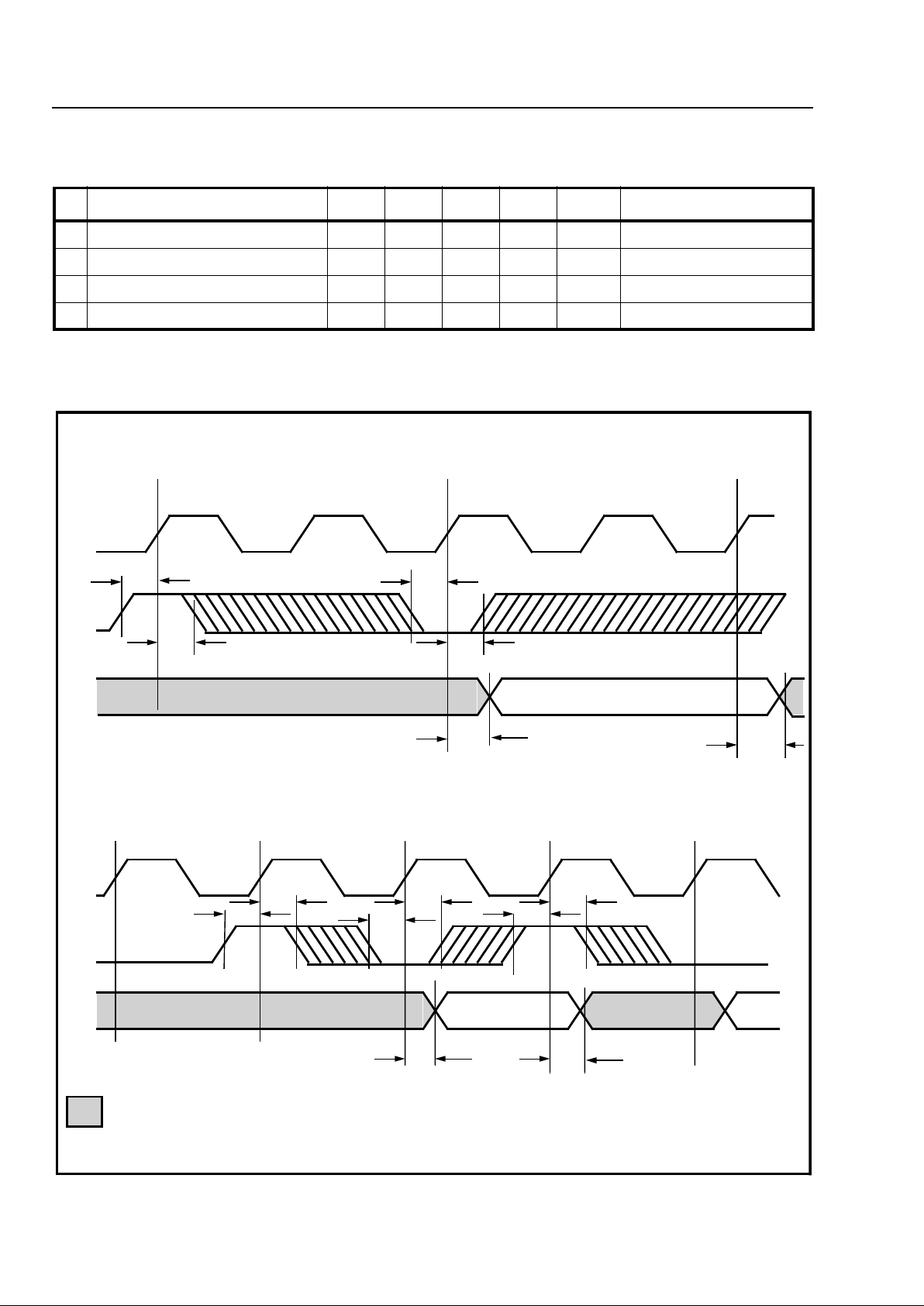
† Timing is over recommended temperature and power supply voltages.
‡ Typical figures are at 25°C and are for design aid only; not guaran teed and no t subject to producti on testing .
Figure 24 - Output Drive Enable Timing
AC Electrical Characteristic s† - Output Drive Enable Timing (see Fig. 24) - Voltages are with respect
to Ground (V
SS
) unless otherwise stated.
Characteristics Sym Min Typ
‡
Max Units Test Conditio ns
1 ODE Setup t
OS
0ns
2 ODE Hold t
OH
20 ns
3 Data Output High Z to Active t
DZA
35 ns CL=30pF
4 Data Output Active to High Z t
DAZ
30 ns
1. Data Memory Mode s And Connec t Memor y Mode - 1
2. Counter, External And Connect Memory Mode - 2
CK
ODE
D0oD15o
CK
ODE
D0oD15o
HIGH IMPEDANCE STATE - OUTPUT DRIVERS DISABLED
CHANNEL N CHANNEL N + 1
t
OS
t
OH
t
OS
t
OH
t
DZA
90%
10%
t
DAZ
CHANNEL CHANNEL
NN + 2
CHANNEL
N + 1
t
OS
t
OH
t
OS
t
OH
t
OS
t
OH
t
DZA
t
DAZ
90%
10%
Page 19
CMOS MT9080
2-119
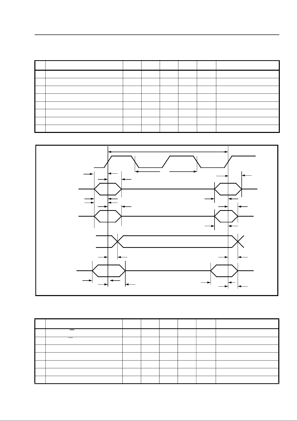
† Timing is over recommended temperature and power supply voltages.
‡ Typical figures are at 25°C and are for design aid only; not guaran teed and not subje ct to producti on testing .
Figure 25 - Data M emo ry, Connect Memory-1 and Sh ift Registe r Mode Timing
† Timing is over recommended temperature and power supply voltages.
‡ Typical figures are at 25°C and are for design aid only; not guaran teed and not subje ct to producti on testing .
AC Electrical Characteristics† - Data Memory, Connect Memory-1 and Shift Register
Mode Timing (See Fig. 25) - Voltages are with respe ct to Ground (V
SS
) unless otherwise stated.
Characteristics Sym Min Typ
‡
Max Units Test Conditions
1 Address Setup t
AS
0ns
2 Address Hold t
AH
18 ns
3 Data Output Delay t
DD
934nsC
L
= 30 pF
4 Data Input Setup t
DS
0ns
5 Data Input Hold t
DH
4ns
6 ME, Mx, My, Mz Setup t
MES
0ns
7 ME, Mx, My, Mz Hold t
MEH
26 ns
8 CK Clock Period t
PCK
60 ns
AC Electrical Characteristics† - External, Connect Memory-2 and Counter Mode Timing
(See Fig. 26) - Voltages are with respe ct to Ground (V
SS
) unless otherwise stated.
Characteristics Sym Min T yp
‡
Max Units Test Conditions
1 ADDR, R/W
Hold Time t
WEH
10 ns
2 ADDR,R/W
Setup Time t
WES
2ns
3 Data Setup t
DS
0ns
4 Data Hold t
DH
4ns
5 Data Output Delay t
DD
934nsC
L
= 30 pF
6 ME, Mx, My, Mz Setup t
MES
0ns
7 ME, Mx, My, Mz Hold t
MEH
26 ns
CK
A0-A15*
ME/Mx/y/z
D0o-D15o
D0i-D15i*
t
AS
t
DH
t
DS
t
DH
t
AH
t
AH
t
AS
t
MES
t
MEH
t
AS
t
MEH
t
MES
t
DD
t
DD
t
DS
t
PCK
Channel Timeslot
*Timing applicable to Data Memory and Shift Register modes only.
Page 20
MT9080 CMOS
2-120
Figure 26 - Exte rn al, Co nne ct M em or y-2 and C ou nt er Mo d e Tim ing
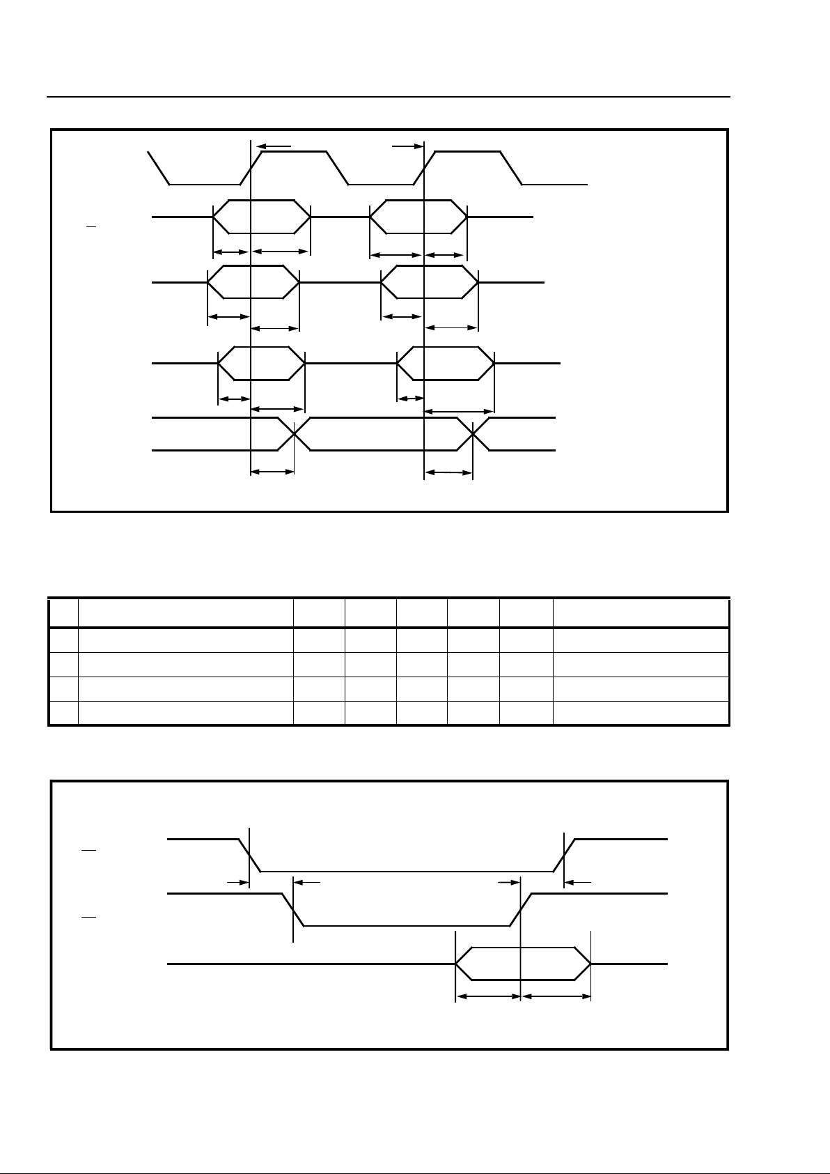
† Timing is over recommended temperature and power supply voltages.
‡ Typical figures are at 25°C and are for design aid only; not guaran teed and no t subject to producti on testing .
Figure 27 - Address Bus Timing in Shift Register Mode
AC Electrical Characterist ics† - Address Bus T iming In Shift Register Mode (See Fig. 27) -
Voltages are with respect to Ground (V
SS
) unless otherwise stated.
Characteristics Sym Min T yp
‡
Max Units Test Conditions
1 A dd re ss Setup t
AS
0ns
2 Add ress Hold t
AH
12 ns
3 C hip Se lect S etu p t
CSS
0ns
4 C hip Se lect H old t
CSH
0ns
CK
A0-A15*,
R/W
**
ME/Mx/y/z
D0i-D15i* *
D0o-D15o
***Timing applicable to External mode only.
Timing applicable to External and Counter modes.
t
WES
t
WEH
t
WES
t
MES
t
MES
t
MEH
t
MEH
t
DS
t
DH
t
DS
t
DH
t
DD
t
DD
t
WEH
Channel Timeslot
CS
DS
A0-A15
t
CSH
t
CSS
t
AS
t
AH
Page 21
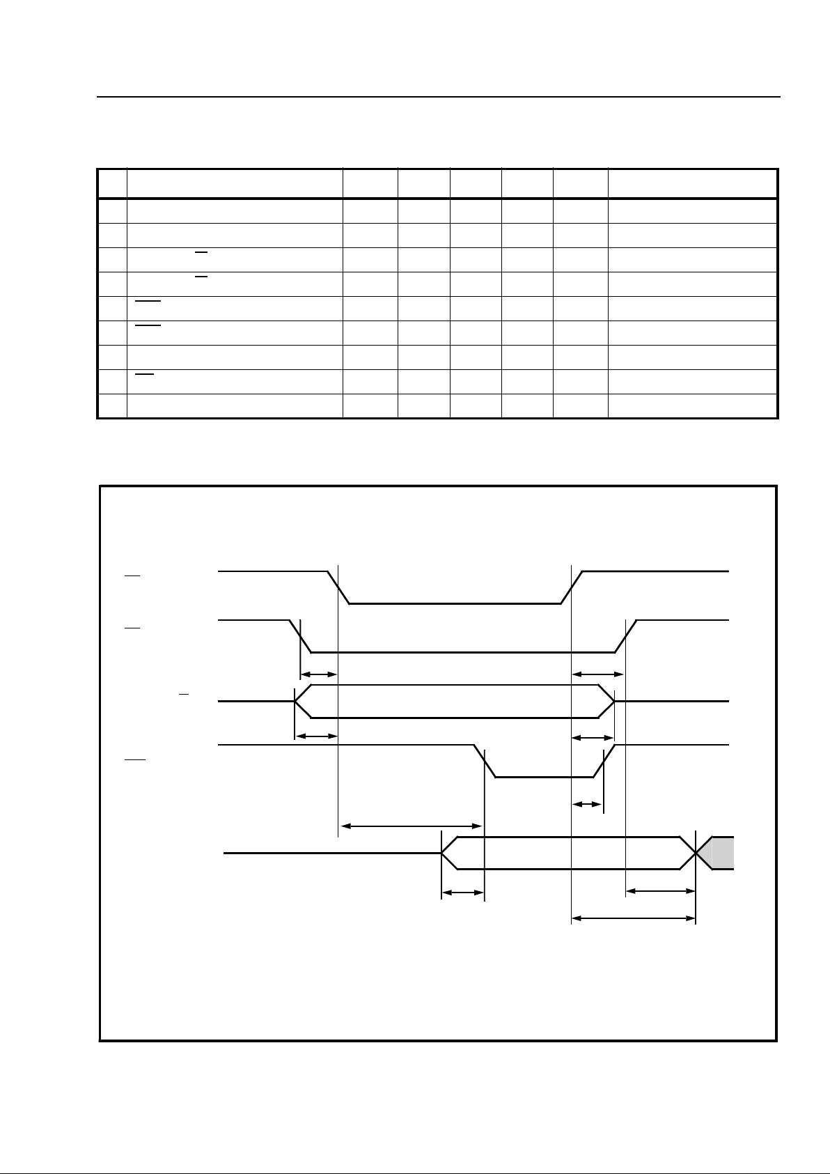
CMOS MT9080
2-121
*T
CK
= Clock (CK) Period
† Timing is over recommended temperature and power supply voltages.
‡ Typical figures are at 25°C and are for design aid only; not guaran teed and not subje ct to producti on testing .
Figure 28 - Microprocessor Read Timing for Connect Memory Mode, Data Memory Mode and
External Mode
AC Electrical Characteristics† - Microprocessor Read Tim ing for Connect Memory, Data
Memory & External Modes (See Fig. 28) - Voltages are with respect to Ground (V
SS
) unless otherwise stated.
Characteristics Sym Min Typ
‡
Max Units Test Conditions
1 Chip Select Setup t
CSS
0ns
2 Chip Select Hold t
CSH
0ns
3 ADDR, R/W
Setup t
AS
0ns
4 ADDR, R/W
Hold t
AH
0ns
5DTA
Delay t
DTAD
4.5 9 TCK*
6DTA
Hold t
DTAH
0ns
7 Valid Data Out to DTA Low t
RD
3T
CK
*
8DS
High to Data Invalid t
DH
027ns
9 Output Data Active to High Z t
DHZ
31 ns
DS
CS
A0-A15, R/W
DTA
Data Bus*
t
CSS
t
CSH
t
AS
t
AH
t
DTAD
t
DTAH
t
RD
t
DHZ
t
DH
* In Data Memory Mode and External Mode, data is clocked out on D0o-D15o; in Connect Memory Mode data is clocked out on
D0i-D15i (bidi rectio n al).
Page 22
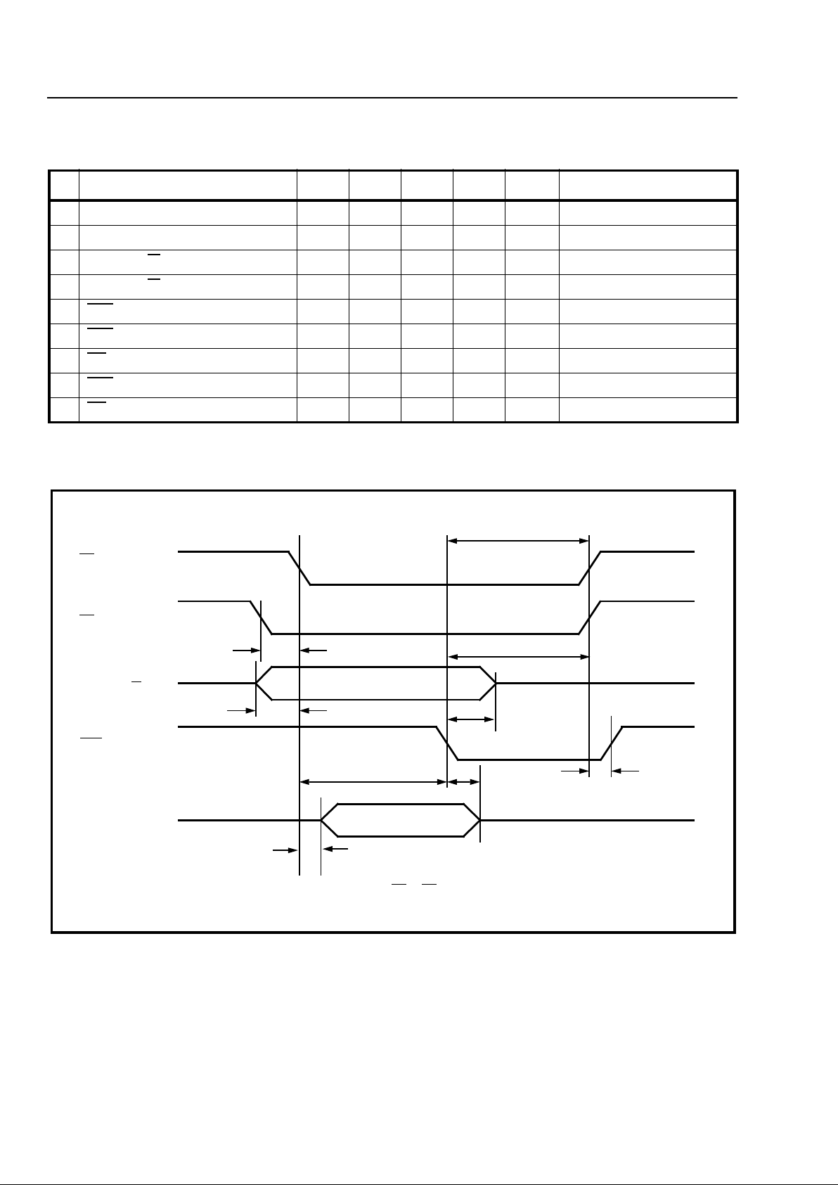
MT9080 CMOS
2-122
*T
CK
= Clock (CK) Period
† Timing is over recommended temperature and power supply voltages.
‡ Typical figures are at 25°C and are for design aid only; not guaran teed and no t subject to producti on testing .
Figure 29 - Mi crop ro ces sor Wri te Tim ing fo r Con ne ct M e mor y Mo de
AC Electrical Characteristics† - Microprocessor Write Timing for Connect Memory Mode
(See Fig. 29) - Voltages are with respect to Ground (V
SS
) unless otherwise stated.
Characteristics Sym Mi n Typ
‡
Max Units Test Conditions
1 Chip Select Setup t
CSS
0ns
2 Chip Select Hold t
CSH
0ns
3 ADDR, R/W
Setup t
AS
0ns
4 ADDR, R/W
Hold t
AH
0ns
5DTA
Delay t
DTAD
4.5 7.5 TCK*
6DTA
Hold t
DTAH
0ns
7DS
Low to Data in Delay t
DD
4.5 TCK*
8DTA
Low to Data in Hold t
DH
0ns
9DS
Hold Time t
DSH
0ns
DS
CS
A0-A15,R/W
DTA
D0-D15i
t
CSS
t
AS
t
DSH
t
CSH
t
AH
t
DTAD t
DH
t
DTAH*
t
DD
* This parameter is specified with respect to the rising edge of DS or CS depending on which signal goes high first.
Page 23
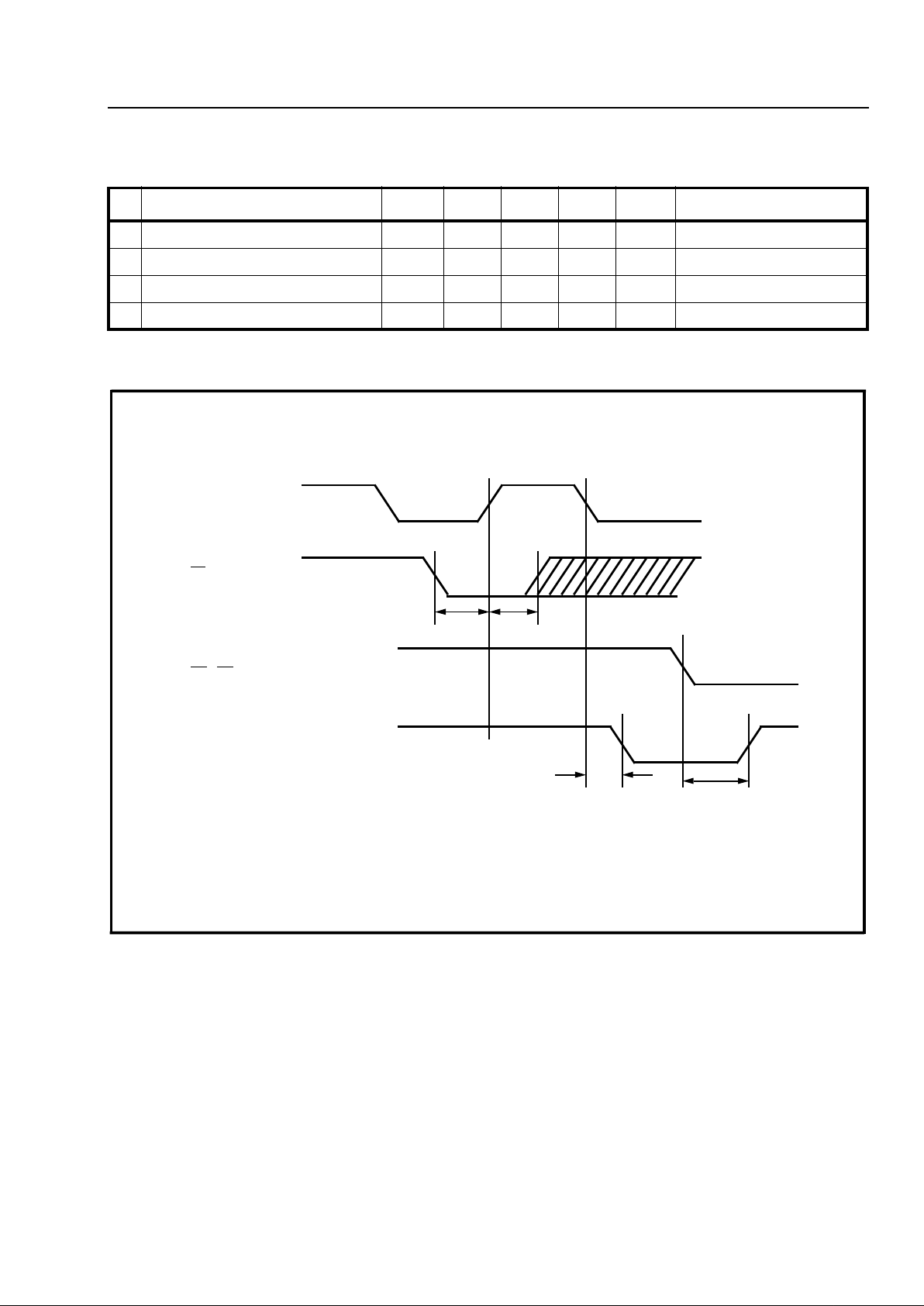
CMOS MT9080
2-123
† Timing is over recommended temperature and power supply voltages.
‡ Typical figures are at 25°C and are for design aid only; not guaran teed and not subje ct to producti on testing .
Figure 30 - Frame Pulse and Change Detect Timing
AC Electrical Characteristics† - Frame Pulse, Clock and Change Detect Timing (See Fig.
30) - Voltages are with respect to Ground (V
SS
) unless otherwise stated.
Characteristics Sym Min Typ
‡
Max Units Test Conditions
1 Frame Pulse Setup t
FPS
6ns
2 Frame Pulse Hold t
FPH
3ns
3 Change Detect Delay t
CDD
38 ns
4 Change Detect Reset Delay t
CDRD
013ns
CK
FP
DS / CS
CD
t
FPS
t
FPH
t
CDD*
t
CDRD
* Assumes change in memory contents detected in previous frame
Page 24

MT9080 CMOS
2-124
NOTES:
 Loading...