

Page 1
4-187
Features
• Complete pri mary ra te 20 48 kbit/s CEPT
transceiver with CRC-4 option
• Selectable HDB3 or AMI line code
• Two frame elastic buffer with 32µs j itter buffer
• Tx and Rx fr ame an d mult ifram e
synchroniza-tion signals
• Frame alignm ent and CRC error coun ters
• Insertion and dete ction of A, B, C, D sign alling
bits with opt iona l debo unce
• Line drive r and rec eive r
• Per channel , overa ll, and re mote l oop aro und
• Digital ph ase det ecto r betw een E 1 line and
ST-BUS
• ST-BUS compatible
• Pin compatible with the MH89790
• Inductorless clock recovery
• Loss of Sign al (LO S) indi cation
• Available in standard, narrow and surface
mount form ats
• Supports si ngle su pply ra il ope ratio n
Applications
• Primary rate ISDN netw ork node s
• Multiplexing equipment
• Private network: PBX to PBX links
Description
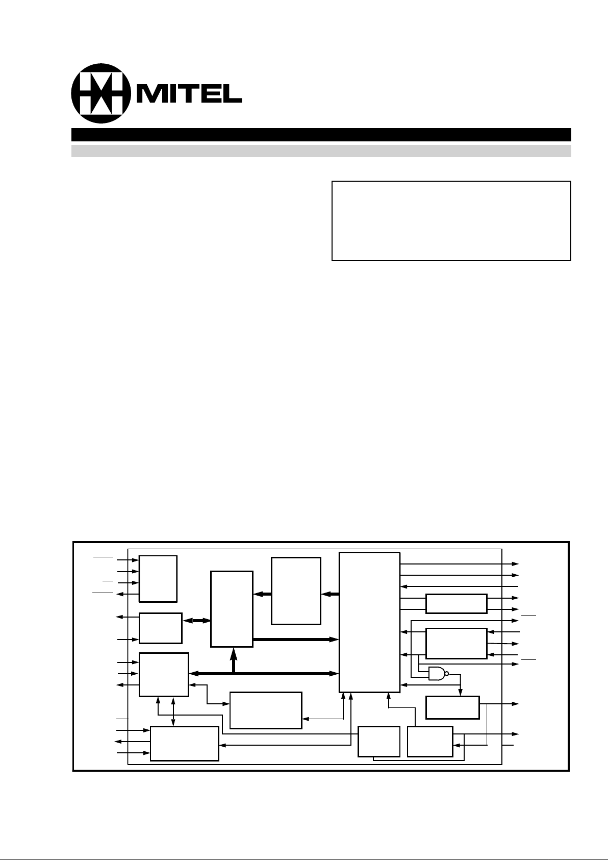
The MH89790B is Mitel’s CEPT PCM 30 interface
solution, designed to meet the latest CCITT
standards PCM 30 format with CRC-4. The
MH89790B provides a complete interface between a
2.048 Mbit/sec digital trunk and Mitel’s Serial
Telecom Bus, the ST-BUS.
The MH89790B is a pin-compatible enhancement of
the MH89790, permitting the removal of the tuneable
inductor and inclusion of the external NAND gate
used for generating RxD.
Figure 1 - Functional Block Diagram
TxMF
C2i
F0i
RxMF
DSTo
DSTi
CSTi0
CSTi1
CSTo
VDD
ADl
XCtl
XSt
PADi
TxG
PADo
OUTA
OUTB
RxA
RxT
LOS
RxR
RxB
E2o
E8Ko
VSS
ST-BUS
Timing
Cicuitry
Data
Interface
Control
Logic
Digital
Attenu-
ator
ROM
2 Frame
Elastic
Buffer
with Slip
Control
ABCD
Signalling RAM
CEPT
Link
Interfac e
Phase
Detector
CEPT
Counter
Clock
Extractor
Receiver
Tran smitter
Serial
Interface
Control
•
•
•
•
•
Ordering Information
MH89790B 40 Pin DIL Hybrid 1.3” row pitch
MH89790BN 40 Pin DIL Hybrid 0.8“ row pitch
MH89790BS 40 Pin Surface Mount Hybrid
0°C to 70°C
ISSUE 5 May 1995
MH89790B
CEPT PCM 30/CRC-4 Framer & Interface
ST-BUS FAMILY
Preliminary Info rmat ion
Page 2
4-188
MH89790B Preliminary Information
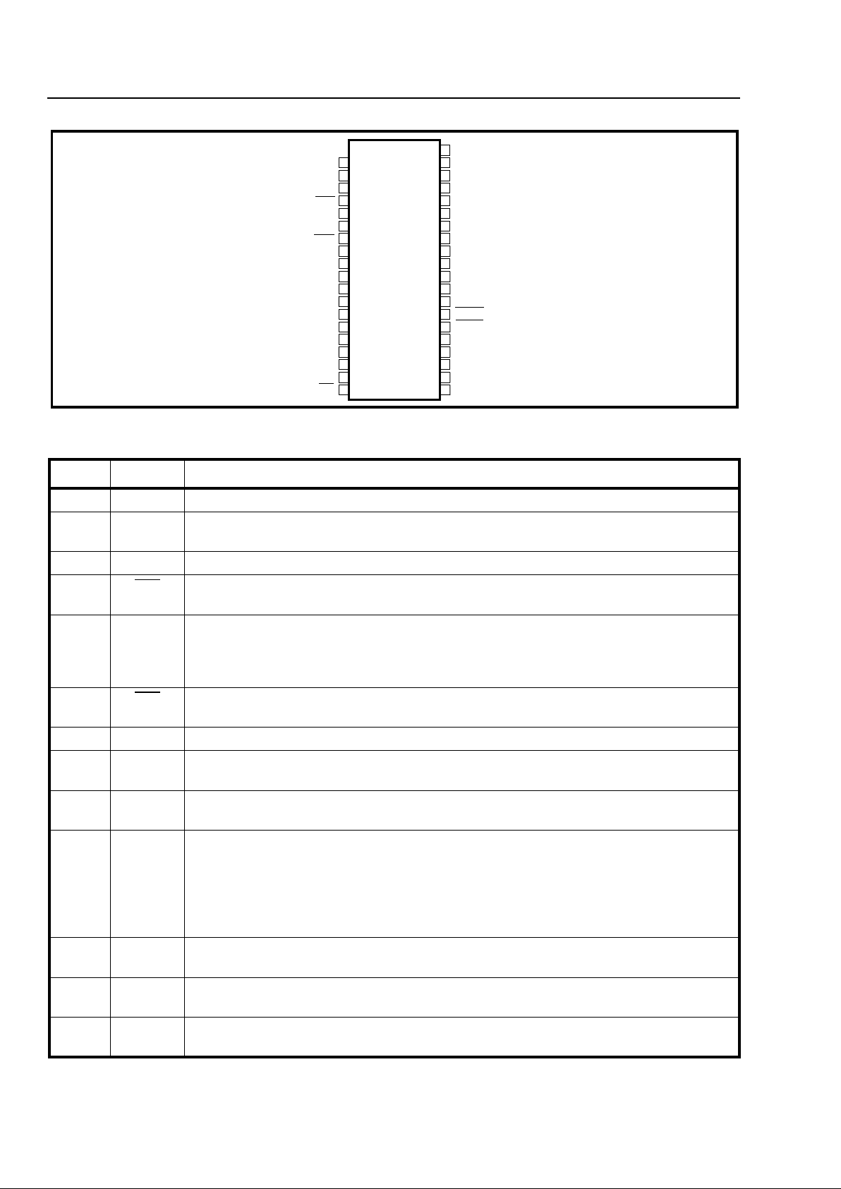
Figure 2 - Pin Connections
Pin Description
Pin # Name Description
2ICInternal Connection . Leave open circuit.
3E2o2048 kHz Extracted Clock (Output): T his clock is extracted by the device from the
received signal. It is used internally to clock in data received at RxT and RxR.
4V
DD
D.C. Power Inp ut. (+5V ).
5RxA
Receive A (Output): The bipolar CEPT signal received by the device at the RxR and
RxT inputs is converted to a unipolar format and output at this pin.
6
7
RxT
RxR
Receive Tip and Receive Ring Inpu ts. The AMI receive signal is input to these pins.
Both inputs should be connected to a center-tapped , center-grounded tran sform er.If the
receive side of the device is not used, these pins must be tied to ground through 1kΩ
resistors.
8RxB
Receive B (Output): The bipolar CEPT signal received by the device at the RxR and
RxT inputs is converted to a unipolar format and output at this pin.
9NCNo Connection.
10 CSTi1 Control ST-BUS Input #1: A 2048 kbit/s stream that contains channel associated
signalling, frame alignment and diagno stic fun ction s.
11 CSTi0 Control ST-BUS Input #0: A 2048 kbit/s stream that contains 30 per channel control
words and two Master Control Words.
12 E8Ko 8 kHz Ex tracted Clock (Output): An 8 kHz output generat ed by dividing the extracted
2048 kHz clock by 256 and aligning it with the received CEPT frame. The 8 kHz signal
can be used for synchronizing the system clock to the extracted 2048 kHz clock. Only
valid when device achieves synchronization (g oes low d uri ng a los s of s ignal or a loss
of basic frame synchronization condition).
E8Ko goes to high impedance when 8kHzSEL = 0 in MCW2.
13 XCtl External Control (Output): An uncommitted external output pin which is set or reset via
bit 1 in Master Control Word 2 on CSTi0. The state of XCtl is updated once per frame.
14 XSt External Statu s: The state of this pin is sampl ed once per frame and the status is
reported in bit 1 of the Master Status Word 1 on CSTo.
15 CS To Control ST -BUS Output: A 2048 kbit/s serial control stream which provides the 16
signalling words, two Master Status Words, Pha se Status Word and CRC Error Count.
IC
E2o
VDD
RxA
RxT
RxR
RxB
NC
CSTi1
CSTi0
E8Ko
XCtl
XSt
CSTo
NC
LOS
NC
NC
NC
NC
VSS
NC
DSTo
NC
OUTB
NC
RxMF
ADl
DSTi
C2i
E2o
F0i
NC
TxMF
OUTA
PADo
TxG
PADi
VSS
2
3
4
5
6
7
8
9
10
11
12
13
14
15
16
17
18
19
20
40
39
38
37
36
35
34
33
32
31
30
29
28
27
26
25
24
23
22
21
Page 3

4-189
Preliminary Information MH89790B
16 ADI Alternate Digit Inversion (Input): If this input is high, the CEPT timeslots which are
specified on CSTi0 as voice channels are ADI coded and decoded. When this bit is low
it disables ADI coding for all channels. This feature allows either ADI or non-ADI codecs
to be used on DSTi and DSTo. Internally pulled with a 4.7kΩ resistor to +V
DD
.
17 DSTi Data ST-BUS Input: This pin accepts a 2048 kbit/s serial stream which contain s the 30
PCM or data channels to be transmitted on t he CEPT trunk.
18 C2i 2048 kbit/s System Clock (In pu t): The master clock for the S T-BUS section of the
chip. All data on the ST-BUS is clocked in on the falling edge of the C2i and output on the
rising edge. The falling edge of C2i is also used to clock out data on the CEPT PCM 30
transmit link.
19 E2o 2048 kHz Extracted Clock (Output): Internally connected to pin 3.
20 F0i
Frame Pulse Input: The ST-BUS frame synchronization signal which defines the
beginning of the 32 channel frame.
21 V
SS
Ground. D.C. Power Return.
22 PA Di PAD Input: Input to the symmetrical resistive 75 ohm T-type line matching circuit. In a
typical application connect this input to the output of the line driving transforme r.
23 TxG Transmit Ground: Common point of the T-type PAD circuit. Connect to GND in a typical
application.
24 PADo PAD Output: Output from the T-type PAD circuit. Output impedance of the PAD is pure
resistive 75Ω.
25 OUTA Output A (Open Collector Output): This is the output of the CEPT transmitter. It is
suitable for use with an external pulse transform er to generate the transmit bipolar line
signal.
26 TxMF
Transmit Multiframe Bou nda ry (Inp ut): This input can be used to set the channel
associated and CRC transmitted multifram e boundary (clear the frame count ers). If a
transmit multiframe signal is not being generated externally to the device, the MH89790B
will internally generate its own mul tifram e when this pin is tie d high.
27 RxMF
Received Multiframe Boundary (Output): An output pulse delim iting the received
multiframe boundary. (This multiframe is not related to the received CRC multiframe. )
28 NC No Connection.
29 OUTB Output B (Open Collector Output): Output of the CEPT transmi tte r. I t is suitable fo r
use with an external pulse tran sfor m er to generate the tra nsmit bipolar line si gnal.
30 NC No Connection.
31 DS To Data ST-BUS Output: A 2048 kbit/s serial output stream which contains the 30 PCM or
data channels received from the CEPT line.
32 NC No Connection.
33 V
SS
Ground. D.C. Power Return.
34 - 37 NC No Connection.
38 LOS Loss of Signal (Output): This pin goes High when 128 contiguous ZEROs are received
on the RxT and RxR inputs. When LOS is High, RxA
and RxB are forced High. LOS is
reset when 64 ONEs are received in a two E1-frame period.
39 - 40 NC No Connection.
Pin Description (Continued)
Pin # Name Description
Page 4

4-190
MH89790B Preliminary Information
Functional Description
The MH89790B is a digital trunk interface
conforming to CCITT Recommendation G.704 for
PCM 30 and I.431 for ISDN. It includes features
such as insertion and detection of synchronization
patterns, optional cyclical redundancy check
(CRC-4) and far end error performance reporting,
HDB3 decoding and optional coding, channel
associated or common channel signalling,
programmable digital attenuation, and a two frame
received elastic buffer. The MH89790B can also
monitor several conditions on the CEPT digital trunk
which include the following: Loss of Signal (LOS)
indication, frame and multiframe synchronization,
received all 1’s alarms, data slips, as well as near
and far end framing and CRC errors.
The system interface to the MH89790B is a serial
bus that operates at 2048 kbit/s known as the
ST-BUS. This serial stream is divided into 125 µs
frames that are made up of 32 x 8 bit channels.
The line interface to the MH89790B consists of split
phase unipolar inputs and outputs which are
supplied from/to a bipolar line receiver/driver,
respectively.
CEPT Interface
The CEPT frame format consists of 32, 8 bit
timeslots. Of the 32 timeslots in a frame, 30 are
defined as information channels, timeslots 1-15 and
17-31 which correspond to telephone channels 1-30.
An additional data channel may be obtained by
placing the device in common channel signalling
mode. This allows use of timeslot 16 for 64 kbit/s
common channel signalling. Synchronization is
included within the CEPT bit stream in the form of a
bit pattern inserted i n to tim e s lot 0. The c o nt ents of
timeslot 0 alternate between the frame alignment
pattern and the non-frame alignment pattern as
described in Figure 3 below. Bit 1 of the frame
alignment and non-frame alignment bytes have
provisions for additional protection against false
synchronization or enhanced error monitoring. This
is described in more detail in the following section.
In order to accomplish multiframe synchronization, a
16 frame multiframe is defined by sending four zeros
in the high order quartet of timeslot 16 frame 0, i.e.,
once every 16 frames (see Figure 4). The CEPT
format has four signalling bits, A, B, C and D.
Signalling bits for all 30 information channels are
transmitted in timeslot 16 of frames 1 to 15. These
timeslots are subdivided into two quartets (see Table
6).
Cyclic Redundancy Check (CRC)
An optional cyclic redundancy check (CRC) has
been incorporated within CEPT bit stream to provide
additional protection against simulation of the frame
alignment signal, and/or where there is a need for an
enhanced error monitoring capability. The CRC
process treats the binary string of ones and zeros
contained in a submultiframe (with CRC bits set to
binary zero) as a single long binary number. This
string of data is first multiplied by x
4
then divided by
the polynomial x
4
+x+1. This process takes place at
both the transmitter and receiver end of the link. The
remainder calculated at the receiver is compared to
the one received with the data over the link. If they
Figure 3 - Allocation of Bits in Timeslot 0 of the CEPT Link
Note 1 : With CRC active, this bit is ignored.
Note 2 : With SiMUX active, this bit transmits SMF CRC re sults in frames 13 and 15.
Note 3 : Reserved for National use.
.
Figure 4 - Allocation of Bits in Timeslot 16 of the CEPT Link
Bit Number
1 2 3 45678
Timeslot 0 containing the
frame alignment signal
Reserved for
International
use
(1)
0 0 11011
Timeslot 0 containing the
non-frame alignment signal
Reserved for
International
use
(2)
1 Alarm indication to the
remote PCM multiplex
equipment
See
Note
#3
See
Note
#3
See
Note
#3
See
Note
#3
See
Note
#3
Timeslot 16 of frame 0 Timeslot 16 of frame 1
• • •
Timeslot 16 of frame 15
0000 XYXX
ABCD bits for
telephone
channel 1
(timeslot 1)
ABCD bits for
telephone
channel 16
(timeslot 17)
ABCD bits for
telephone
channel 15
(timeslot 15)
ABCD bits for
telephone
channel 30
(timeslot 31)
Page 5

4-191
Preliminary Information MH89790B
are the same, it is of high probability that the
previous submultiframe was received error free.
The CRC procedure is based on a 16 frame
multiframe which is divided into two 8 frame
submultiframes (SMF). The frames which contain
the frame alignment pattern contain the CRC bits, C
1
to C4, respectively, in the bit 1 position. The frame
which contains the non-frame alignment pattern
contains within the bit 1 position, a 6 bit CRC
multiframe alignment signal and two spare bits (in
frames 13 and 15) which are used for CRC error
performance reporting (refer to Figure 5). During the
CRC encoding procedure the CRC bit positions are
initially set at zero. The rem ainder of the calculation
is stored and inserted into the respective CRC bits of
the next SMF. The decoding process repeats the
multiplication/division process and compares the
remainder with the CRC bits received in the next
SMF.
The two spare bits (denoted Si1 and Si2 in Figure 5)
following the 6-bit CRC mu ltiframe alignment signal
can be used to monitor far-end error performance.
The results of the CRC-4 comparisons for the
previously received SMFII and SMFI are encoded
and transmitted back to the far end in the Si bits
(refer to Table 1).
ST-BUS Interface
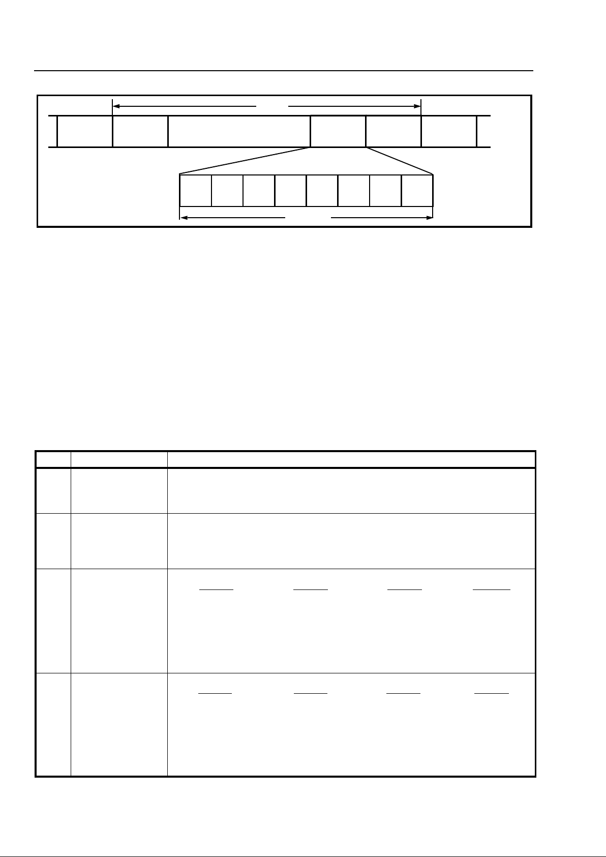
The ST-BUS is a synchronous time division
multiplexed serial bus with data streams operating at
2048 kbit/s and configured as 32, 64 k bit/s channels
(refer Figure 6). Synchronization of the data transfer
is provided from a frame pulse which identifies the
frame boundaries and repeats at an 8 kHz rate.
Figure 2 shows how the frame pulse (F0i
)
defines the ST-BUS frame boundaries. All data is
clocked into the device on the falling edge of the
2048 kbit/s clock (C2i), while data is clocked out on
the rising edge of the 2048 kbit/s clock at the start of
the bit cell.
Table 1. Coding of Spar e Bits Si1 and Si 2
Si1 bit
(frame
13)
Si2 bit
(frame
15)
Meaning
11
CRC results for both SMFI, II a re
error free.
10
CRC result for SMFII is in error.
CRC result for SMFI is error free.
01
CRC result for S MFII is erro r fre e.
CRC result for SMFI is in error.
00
CRC results for both SMFI, II a re
in error.
Figure 5 - CRC Bit Allocation and Submultiframing
Note 1 : Remote Alarm. Keep at 0 for normal operation.
Note 2 : Reser ved for Nati onal use. Keep at 1 for norma l opera tion .
Note 3 : Used to monitor far-e nd CRC e rro r performan ce.
Multiple Fr am e
Componen t
Frame Type
CRC
Frame #
Timeslot Ze ro
12345678
Frame Alignment Signal 0 C
1
0011011
Non-Frame Alignment Signal 1
01A
(1)
Sn
(2)
Sn
(2)
Sn
(2)
Sn
(2)
Sn
(2)
S Frame Alignment Signal 2 C
2
0011011
M Non-Frame Alignment Signal 3
01A
(1)
Sn
(2)
Sn
(2)
Sn
(2)
Sn
(2)
Sn
(2)
F Frame Alignment Signal 4 C
3
0011011
Non-Frame Alignment Signal 5
11A
(1)
Sn
(2)
Sn
(2)
Sn
(2)
Sn
(2)
Sn
(2)
I Frame Alignment Signal 6 C
4
0011011
Non-Frame Alignment Signal 7
01A
(1)
Sn
(2)
Sn
(2)
Sn
(2)
Sn
(2)
Sn
(2)
Frame Alignment Signal 8 C
1
0011011
S Non-Fr ame Alignment Signal 9
11A
(1)
Sn
(2)
Sn
(2)
Sn
(2)
Sn
(2)
Sn
(2)
M Frame Alignment Signal 10 C
2
0011011
F Non-Frame Alignment Signal 11
11A
(1)
Sn
(2)
Sn
(2)
Sn
(2)
Sn
(2)
Sn
(2)
Frame Alignment Signal 12 C
3
0011011
I Non-Frame Alignment Signal 13 Si1
(3)
1A
(1)
Sn
(2)
Sn
(2)
Sn
(2)
Sn
(2)
Sn
(2)
I Frame Alignment Signal 14 C
4
0011011
Non-Frame Alignment Signal 15 Si2
(3)
1A
(1)
Sn
(2)
Sn
(2)
Sn
(2)
Sn
(2)
Sn
(2)
indicates position of CRC-4 multiframe alignment signal
Page 6
4-192
MH89790B Preliminary Information
Figure 6 - ST-BUS Stream Form at
CHANNEL
31
030
BIT
CHANNEL
CHANNEL
CHANNEL
CHANNEL
31 0
BIT BIT
BIT
BIT BIT BIT
BIT
• • •
Least
Significant
Bit (Last)
Most
Significant
Bit (First)
(8/2.048 )µ s
125µs
7654321
0
Data Input (DSTi)
The MH89790B receives information channels on
the DSTi pin. Of the 32 available channels on this
serial input, 30 are defined as information channels.
They are channels 1-15 and 17-31. These 30
timeslots are the 30 telephone channels of the CEPT
format numbered 1-15 and 16-30.
Timeslot 0 and 16 are unused to allow the
synchronization and signalling information to be
inserted, from the Control Streams (CSTi0 and
CSTi1). The relationship between the input and
output ST-BUS stream and the CEPT line is
illustrated in Figures 7 to 11. In common channel
signalling mode timeslot 16 becomes an active
channel. In this mode channel 16 on DSTi is
transmitted on timeslot 16 of the CEPT link
unaltered. This mode is activated by bit 5 of channel
31 of CSTi0.
Control Input 0 (CSTi0)
All the necessary control and signalling information
is input through the two control streams. Control
ST-B US input number 0 (CSTi0) contains the control
informat ion th at is asso ciated wit h each inform ation
channel. Each control channel contains the per
channel digital attenuation information, the individual
Table 2. Per Chan nel Co ntro l Word: Data Form at for CSTi0 Cha nnels 0-14, an d 16-3 0
BIT NAME DESCRIPTION
7 DATA Data Channel: If ‘1‘, then the controlled timeslot on the CEPT 2048 kbit/s link is treated as a
data channel; i .e., no ADI encoding or decoding is performed on transmission or r e ception,
and digital attenuation is disabled. If ‘0‘, then the state of the ADI pin determines whether or
not ADI encoding and decoding is performed.
6 LOOP Per-Channel Loopback: If ‘1‘, then the controlled timeslot on the transmitted CEPT 2048
kbit/s link is looped internally to replace the data on the corresponding received ti me slot. If
‘0‘, then this function is disabled. This function only operates if frame synchronization is
received from the CEPT link. If more than one channel is looped per frame only the first one
will be ac t i v e.
5,4,3 RX PAD4,2,1 Receive Attenuation Pad: Per timeslot receive attenuation control bits.
RXPAD4
0
0
0
0
1
1
1
1
RXPAD2
0
0
1
1
0
0
1
1
RXPAD1
0
1
0
1
0
1
0
1
Gain (dB)
0
-1
-2
-3
-4
-5
-6
1
2,1,0 TXPAD4,2,1 Transmit Attenuation Pad: Per timeslot transmit attenuation control bits.
TXPAD4
0
0
0
0
1
1
1
1
TXPAD2
0
0
1
1
0
0
1
1
TXPAD1
0
0
1
0
1
0
1
0
Gain (dB
)
0
-1
-2
-3
-4
-5
-6
1
Page 7

4-193
Preliminary Information MH89790B
Figure 7 - Relationship between Input DSTi Channels and Transmitted CEPT Timeslots
Figure 8 - Relationship between Received CEPT Timeslots and Output DSTo Channels
Figure 9 - Relationship between Input CSTi0 Channels and Controlled CEPT Timeslots
Figure 10 - Relationship between Input CSTi1 Channels and Transmitted CEPT Frames
Figure 11- Relationship between Received CEPT Frames and Output CSTo Channels
- *Denotes Unused Channel (CSTo output is not put in high impedance state) -CCS Denotes Signa lling Chan ne l i f C o m mo n C ha nn el S i gn al lin g Mode Sele c ted
- A Denotes Frame-Alignment Frame -S1 Denotes Master Status Word 1 (MSW1)
- N Denotes Non Frame-Alignment Frame -S2 Denotes Ph as e Sta tus W o rd (PSW)
- C1, C2, C3 Deno te s Ma s ter C on trol Words 1 ,2 ,3 -S3 Denotes CRC Error Count
- SIG Denotes Signalling C h an ne l -S4 Denotes Master Status Word 2 (MSW2)
DSTi
Channel #
0 1 2 3 4 5 6 7 8 9 10111213141516171819202122232425262728293031
CEPT
Timeslot #
1 2 3 4 5 6 7 8 9 101112131415
CCS
17 18 19 20 21 22 23 24 25 26 27 28 29 30 31
DSTi
Channel #
0 1 2 3 4 5 6 7 8 9 10111213141516171819202122232425262728293031
CEPT
Timeslot #
0123456789101112131415
SIG
17 18 19 20 21 22 23 24 25 26 27 28 29 30 31
CSTi0
Channel #
012345678910111213141516171819202122232425262728293031
Device Control C1 C2
CEPT Channel #
Control Word
123456789101112131415 171819202122232425262728293031
CSTi1
Channel #
0 1 2 3 4 5 6 7 8 9 10111213141516171819202122232425262728293031
Device Control C3*************
CEPT
FRAME #
CHANNEL #
0
16
1
16
2
16
3
16
4
16
5
16
6
16
7
16
8
16
9
16
10
16
11
16
12
16
13
16
14
16
15
16
A
0
N
0
CSTo
Channel #
0 1 2 3 4 5 6 7 8 9 10 11 12 13 14 15 16 17 18 19 20 21 22 23 24 25 26 27 28 29 30 31
Device Status S1S2S3S4**********
CEPT
FRAME #
TIMESLOT #
0
16
1
16
2
16
3
16
4
16
5
16
6
16
7
16
8
16
9
16
10
16
11
16
12
16
13
16
14
16
15
16
A
0
N
0
Page 8

4-194
MH89790B Preliminary Information
Table 3. Mast er C ontrol Wor d 1 (M CW1): Dat a Form at for C STi0 Chan nel 15
Table 4. Master Contr ol Word 2 (M CW2): D ata Forma t for CSTi0 Ch ann el 31
Table 5. Multifra me Alignm ent Sign al:D ata Forma t for CSTi1Ch annel 0 on the Transmitted CEPT Link
BIT NAME DESCRIPTION
7 (N/A) Keep at ‘1‘ for normal operation.
6 LOOP16 Channel 16 Loopback: If ‘1‘, then timeslot 16 on the transmitted CEPT 2048 kbit/s link is
looped internally to replace the data received on timeslot 16. If ‘0,‘ then this function is
disabled.
This function only operates if frame synchronization is received from the CEPT link and only a
single timeslot can be looped within the frame.
5,4 (N/A) Keep at ‘1‘ for normal operation.
3,2,
1
& 0
NDBD, NDBC,
NDBB
& NDBA
Signalling Bit Debounce: If ‘1‘, then no debouncing is applied to the received A, B, C or D
signalling bits. If ‘0‘, then the received A, B, C or D signalling bits are debounced for between
6 and 8 ms.
BIT NAME DESCRIPTION
7 (N/A) Keep at ‘1‘ for normal operation.
6 (N/A) Keep at ‘0‘ for normal operation.
5 CCS Common Channel Signalling: If 1, then the MH89790B operates in its common channel
signalling mode. Channel 16 on the DSTi pin is transmitted on timeslot 16 of the CEPT link, and
timeslot 16 from the received CEPT link is output on channel 16 on the DSTo pin. Channel 15 on
the CSTi0 pin contains the information for the control of timeslot 16. Channels 0 to 15 on CSTi 1
and CSTo are unused.
If ‘0‘, the device is in channel associated signalling mode where channel 16 is used to transmit
the ABCD signalling bits.
4 8kHzSEL 8kHz Select: If ‘1‘, then an 8 kHz signal synchronized to the received CEPT 2048 kbit/s link is
output on the E8Ko pin. This feature is only valid when frame synchronization is received from
the CEPT link.
If ‘0‘, then the E8Ko pin goes into its high impedance state.
3 TXAIS Transmit Alarm Indication Signal:
If ‘1‘, then an all 1’ s alarm signal is transmitted on all timeslots.
If ‘0‘, then the timeslots functions normally.
2 TXTS16AIS Transmit Timeslot 16 Alarm Indication Signal:
If ‘1‘, then an all 1’s alarm signal is transmitted on timeslot 16.
If ‘0‘, then timeslot 16 functions normally.
1 XCtl External Control:
If ‘1‘, then the XCtl pin is driven high.
If ‘0‘, then the XCtl pin is driven low.
0 (N/A) (unused)
BIT NAME DESCRIPTION
7-4 MA1-4 Transmit Multiframe Alignment Bits 1 to 4: These bits are transmitted on the CEPT 2 048
kbit/s link in bit positions 1 to 4 of timeslot 16 of frame 0 of the multiframe. They should be kept at
‘0‘ to allow multiframe alignment to be detected.
3X1This bit is transmitted on the CEPT 2048 kbit/s link in bit position 5 of timeslot 16 of frame 0 of the
multiframe. It is a spare bit which should be kept at ‘1‘ if unused.
2YThis bit is transmitted on the CEPT 2048 kbit/s link in bit position 6 of timeslot 16 of frame 0 of the
multiframe. It is used to indicate the loss of multiframe alignment to the remote end of the link. A
‘1‘ on this bit is the signal that multiframe alignment on the received link has been lost. A ‘0’
indicates that multiframe alignment is detected.
1,0 X2,X3 These bits are transmitted on the CEPT 2048 kbit/s link in bit positions 7 and 8 respectively, of
timeslot 16 of frame 0 of the multiframe. They are spare bits which should be kept at ‘1‘ if unused.
Page 9

4-195
Preliminary Information MH89790B
loopback control bit, and the voice or data channel
identifier, see Table 2. When a channel is in data
mode (B7 is high) the digital attenuation and
Alternate Digit Inversion are disabled. It should be
noted that the control word for a given information
channel is input one timeslot early, i.e., channel 0 of
CSTi0 controls channel 1 of DSTi. Channels 15 and
31 of CSTi0 contain Master Control Words 1 and 2
(MCW1, MCW2) which are used to set up the
interface feature as seen by the respective bit
functions of Tables 3 and 4.
Table 6. Channel Associated Signalling: Data Format for CSTi1 Channels 1 to 15
Table 7. Frame-Alignment Signal: Data Format for CSTi1 Channel 16
Table 8. Non-Frame-Alignment Signal: Data Format for CSTi1 Channel 17
BIT NAME DESCRIPTION
7,
6,
5
& 4
A(N),
B(N),
C(N)
& D(N)
Transmit Signalling Bits for Channel N: These bits are transmitted on the CEPT 2048 kbit/s
link in bit positions 1 to 4 of timeslot 16 in frame N, and are the A, B, C and D signalling bits
associated with telephone channel N. The value of N lies in the range 1 to 15 and refers to the
channel on the CSTi1 channel from which the bits are sourced, the telephone channel with which
the bits are associated and the frame on the CEPT link on which the bits are transmitted. For
example, the bits input on the CSTi1 pin on channel 3 are associated with telephone channel 3,
which is timeslot 3 of the CEPT link, and are transmitted on bits positions 1 to 4 of timeslot 16 in
frame 3 of each multiframe on the CEPT link . If bits B, C or D are not used they should be given
the values ‘1, 0‘ and ‘1‘ respectively. The combination ‘0000‘ for ABCD bits should not be used f or
telephone channels 1 to 15 as this would interfere with multiframe alignment.
3,
2,
1
& 0
A(N+15),
B(N+15),
C(N+15)
& D(N+15)
Transmit Signalling Bits for Channel N+15: These bits are transmitted on the CEPT 2048
kbit/s link in bit positions 5 to 8 of timeslot 16 in frame N, and are the A, B, C and D signalling bits
associated with telephone channel N+15. The value of N lies in the range 1 to 15 and refers to
both the channel on the CSTi1 stream where the bits are supplied and the frame on the CEPT
link on which the bits are transmitte d, and indirectly indicates the telephone channel with which
the bits are are associated. For example, the bits input on the CSTi1 pin on channel 3 are
associated with telephone channel 18, which is timeslot 19 of the CEPT link, and are transmitted
in bits positions 5 to 8 of timeslot 16 in frame 3 of each multiframe on the CEPT link .
BIT NAME DESCRIPTION
7 IU0 International U se 0: When CRC is disabled, this bit is transmitted on the CEPT 2048 kbit/s link
in bit position 1 of timeslot 0 of frame-alignment frames . It is reserved for international use and
should be kept at ‘1’ when not used. If CRC is enabled, this bit is not used.
6-0 FAF2-8 Transmit Frame Alignment Signal Bits 2 to 8: These bits are transmitted on the CEPT 2048
kbit/s link in bit positions 2 to 8 of timeslot 0 of frame-alignment frames. These bits form the
frame alignment signal and should be set to ‘00110 11‘.
BIT NAME DESCRIPTION
7 IU1 International U se 1: When the CRC is disabled and SiMUX bit in MCW3 is disabled, this bit is
transmitted on the CEPT 2048 kbit/s link in bit position 1 of timeslot 0 of non-frame-alignment
frames . It is reserved for international use and should be kept at ‘1‘ when not used. If CRC is
enabled and SiMUX is disabled, this bit is transmitted in bit 1 of timeslot 0 for frame 13 and 15. If
both CRC and SiMUX are enabled, then this bit is not used.
6 NFAF Transmit Non-Frame Alignment Bit: This bit is transmitted on the CEPT 2 048 kbit/s link in bit
position 2 of timeslot 0 of non-frame-alignment frames . In order to differentiate between
frame-alignment frames and non-frame-alignment frames, this bit should be kept at ‘1‘.
5 ALM Non-Frame Alignment Alarm: This bit is transmitted on the CEPT 2048 kbit/s link in bit position
3 of timeslot 0 of non-frame-alignment frames . It is used to signal an alarm to the remote end of
the CEPT link. The bit should be set to ‘1‘ to signal an alarm and should be kept at ‘0‘ under
normal operation.
4-0 NU1-5 National Use: These bits are transmitted on the CEPT 2048 kbit/s link in bit positions 4 to 8 of
timeslot 0 of non-frame-alignment frames . These bits are reserved for national use, and on
crossing international borders they should be set to ‘1‘.
Page 10

4-196
MH89790B Preliminary Information
Table 9. Master Contr ol Word 3 (M CW3): D ata Forma t for CSTi1 Ch ann el 18
Table 10. Received Multiframe Alignment Signal: Data Format for CSTo Channel 0
BIT NAME DESCRIPTION
7N/AKeep at zero for normal operation.
6SiMUXWhen set to ‘1’, this bit will cause the SMFI CRC result to be transmit ted in the next outgoing Si1
bit in frame 13 and the SMFII CRC result to be transmitted in the next outgoing Si2 bit in frame
15.
5 RMLOOP Remote Loopback: If set the RxT and RxR signals are looped to OUTA and OUTB,
respectively.
4 HDB3en
Enable HDB3 Encoding: A ’1’ will disable the HDB3 line coding and transmit the information
transparently.
3 Maint Maintenance: A ’1’ will force a complete reframe if the CRC multiframe synchro- ni zat ion is not
achieved within 8 ms of frame synchronization. Reframe will also be generated if more than 914
CRC errors occur within a one second interval (CRC error counter is reset with every one second
interval). A ’0’ will disable this option.
2 CRCen Enable Cyclical Redundancy Check: A ’1’ will enable the CRC gener ation on the transmit
data. A ’0’ will disable the CRC generator. The CRC receiver is always active regardless of the
state of CRCen.
1 DGLOOP Digit al Loopack: When set, the transmitted signal is looped around from DSTi to DSTo. The
normal received data is interrupted.
0 ReFR Force Reframe: If set, for at least one frame, and then cleared the chip will begin to search for a
new frame position when the chip detects the change in state fr om high to low. Only the change
from high to low will cause a reframe, not a continuous low level.
BIT NAME DESCRIPTION
7-4 MA1-4 Receive Multiframe Alignment Bits 1 to 4: These are the bits which are received from the
CEPT 2048 kbit/s link in bit positions 1 to 4 of timeslot 16 of frame 0 of the multiframe. They
should all be ‘0‘.
3X1This is the bit which is received on the CEPT 2048 kbit/s link in bit position 5 of timeslot 16 of
frame 0 of the multiframe. It is a spare bit which should be ‘1‘ if unused . It is not debounced.
2YThis is the bit which is received on the CEPT 2048 kbit/s link in bit position 6 of timeslot 16 of
frame 0 of the multiframe. It is used to indicate the loss of multiframe alignment at the remote end
of the link. A ‘1‘ on this bit is the signal that multiframe alignment at the remote end of the link has
been lost. A ‘0‘ indicates that multiframe alignment is detected. It is not debounced.
1,0 X2,X3 These are the bits which are received on the CEPT 2048 kbit/s link in bit positions 7 and 8
respectively, of timeslot 16 of frame 0 of the multiframe. They are spare bits which should be ‘1‘ if
unused. They are not debounced.
Control Input 1 (CSTi1)
Control ST-BUS input stream number 1 (CSTi1)
contains the synchronization information and the A,
B, C & D signalling bits for insertion into timeslot 16
of the CEPT stre am (re fer to Tables 5 to 8 ). Timesl ot
0 contains the four zeros of the multiframe alignment
signal plus the XYXX bits (see Figure 4). Channels 1
to 15 of CSTi1 contain the A, B, C & D signalling bits
as defined by the CEPT format (see Figure 4), i.e.,
channel 1 of CSTi1 contains the A, B, C & D bits for
DSTi timeslots 1 and 17. Channel 16 contains the
frame alignment signal, and channel 17 contains the
non-frame alignment signal (see Figure 3). Channel
18 contains the Master Control Word 3 (see Table 9).
Figure 10 shows the relationship between the control
stream (CSTi1) and the CEPT stream.
Control Output (CSTo)
Control ST-BUS output (CSTo) contains the
multiframe signal from timeslot 16 of frame 0 (see
Table 10). Signalling bits, A, B, C & D for each CEPT
channel are sourced from timeslot 16 of frames 1-15
and are output in channels 1-15 on CSTo , as shown
in Table 11. The frame alignment signal and
non-frame alignment signal, received from timeslot
0 of alternate frames are output in timeslots 16 and
17, as shown in Tables 12 and 13.
Page 11

4-197
Preliminary Information MH89790B
Table 11. Received Channel Associated Signalling: Data Format for CSTo Channels 1 to 15
Table 12. Received F rame Al ignm ent S ignal: Data F ormat for CS To Channel 16
Table 13. Received Non-Frame Alignment Signal: Data Format for CSTo Channel 17
BIT NAME DESCRIPTION
7,
6,
5
& 4
A(N),
B(N),
C(N)
& D(N)
Receive Signalling Bits for Channel N: These ar e the bits which are received from the CEPT
2048 kbit/s link in bit positions 1 to 4 of timeslot 16 in frame N (frame #), and are the A, B, C and
D signalling bits associated with telephone channel N . The v alue of N l ies in the range 1 to 15 and
refers to the channel on the CSTo stream on which the bits are output, the telephone channel with
which the bits are associated and the frame on the CEPT link on which the bits are received. For
example, the bits output on the CST o stream on channel 3 are associated with telephone channel
3, which is timeslot 3 of the CEPT link, and are recei ved on bits positions 1 to 4 of timeslot 16 in
frame 3 of each multiframe on the CEPT link . If bits B, C or D are not used they should have the
values ‘1, 0‘ and ‘1’, respectively. The combination ‘0000‘ for ABCD bits should not be found for
telephone channels 1 to 15 as this implies interference with multiframe alignment.
3,
2,
1
& 0
A(N+15),
B(N+15),
C(N+15)
& D(N+15)
Receive Signalling Bits for Channel N+ 15: These are the bits which are received from the
CEPT 2048 kbit/s link in bit positions 5 to 8 of timeslot 16 in frame N, and are the A, B, C and D
signalling bits associated with telephone channel N+15. The value of N lies in the range 1 to 15
and refers to both the channel o n th e CSTo stream where the bits are output and the frame on the
CEPT link on which the bits are received, and indirectly indicates the telephone channel with
which the bits are are associated. The associated channel is N+15.
For example, the bits output on the CSTo stream on channel 3 are associated with telephone
channel 18, which is timeslot 19 of the CEPT link, and are received on bits positions 5 to 8 of
timeslot 16 in frame 3 of each multiframe on the CEPT link .
BIT NAME DESCRIPTION
7 IU0 International Use 0: This is the bit which is received from the CEPT 2048 kbit/s link in bit
position 1 of timeslot 0 of frame-alignment frames . It is reserved for the CRC remainder or for
international use.
6-0 FAF2-8 Frame Alignment Signal Bits 2 to 8: These are the bits which are received from the CEPT
2048 kbit/s link in bit positions 2 to 8 of timeslot 0 of frame-alignment frames . These bits fo rm the
frame alignment signal and should have the values of ‘0011011‘.
BIT NAME DESCRIPTION
7 IU1 International Use 1: This is the bit which is received from the CEPT 2048 kbit/s link in bit
position 1 of timeslot 0 of non-frame-alignment frames. It is reserved for CRC framing bits or
international bits.
6 NFAF Receive Non-Frame Alignment Bit: This is the bit which is received from the CEPT 2048 kbit/s
link in bit position 2 of timeslot 0 of non-frame-alignment frames . This bit should be ‘1‘ in order to
differentiate between frame-alignment frames and non-frame-alignment frames.
5 ALM Non-Frame Alignment Alarm: This bit is received from the CEPT 2048 kbit/s link in bit position
3 of timeslot 0 of non-frame-alignment frames . It is used to signal an alarm from the remote end
of the CEPT link. This bit should have the value ‘0‘ under normal operation and should go to ‘1 ‘to
signal an alarm.
4-0 NU1-5 National Use: These are the bits which are received on the CEPT 2048 kbit/s link in bit positions
4 to 8 of timeslot 0 of non-frame-alignment frames . These bits are reserved for national use, and
on crossing international borders they should have the value ‘1‘.
Page 12

4-198
MH89790B Preliminary Information
Table 14. Mas ter S tatus Wo rd 1 (MS W1): Da ta Form at for CSTo Channel 18
Table 15. Phase S tatus Word (P SW): Data Format fo r CSTo Channel 19
Table 16. CRC Error Co unt: Data F orma t for CSTo Channel 20
Table 17. Mas ter S tatus Wo rd 2 (MS W2): Da ta Form at for CSTo Channel 21
BIT NAME DESCRIPTION
7 TFSYN Frame Sync: This bit goes to ‘1‘ to indicate a loss of frame alignment synchronization by the
MH89790B. It goes to ‘0‘ when frame synchronization is detected.
6 MFSYN
Multiframe Sync: This bit goes to ‘1‘ to indicate a loss of multiframe synchronization by the
MH89790B. It goes to ‘0‘ when multiframe synchronization is detected.
5 ERR Frame Alignment Error: This bit changes state when 16 or more errors have been detected in
the frame alignment signal. It will not change state more than once every 128 ms.
4 SLIP Control Slip: This bit changes state when a slip occurs between the received CEPT 2048 kbit/s
link and the 2048 kbit/s ST-BUS.
3 RXAIS Receive Alarm Indication Signal: This bit goes to ‘1‘ to signal that an all-ones alarm signal has
been detected on the received CEPT 2048 kbit/s link. It goes to ’0’ when the all-ones alarm
signal is removed.
2 RXTS16AIS Receive Timeslot 16 Alarm Indication Signal: This bit goes to ‘1‘ to signal that an all-ones
alarm signal has been detected on channel 16 of the received CEPT 2048 kbit/s link. It goes to
‘0‘ when the all-ones alarm signal is removed.
1 XSt External Status: This bit contains the data sampled once per frame at the XSt pin.
0N/A(Unused).
BIT NAME DESCRIPTION
7 - 3 TxTSC Transmit Timeslot Count: The value of these five bits indicate the timeslot count between the
ST-BUS frame pulse and the rising edge of E8Ko.
2 - 0 TxBTC Transmit Bit Count: The value of th ese three bits indicate th e bit position within the tim eslot
count reported in TxTSC abov e.
BIT NAME DESCRIPTION
7 - 0 CERC CRC Error Counter: This byte is the CRC error counter. The counter will wrap around once it
reaches FF count. If maintenance option is activated, the cou nter will reset onc e per secon d.
BIT NAME DESCRIPTION
7Si2The received Si bit in frame 15 is reported in this bit. Si2 will be updated after each
RXMF
pulse (pin 23).
6Si1The received Si bit in frame 13 is reported in this bit. Si1 will be updated after each
RXMF
pulse (pin 23).
5-4 NA Unused.
3 CRCTimer CRC Timer: Transition from 1 to 0 indicates the start of one second interval in which CRC errors
are accumulated. This bit stay high for 8 ms.
2 CRCRef CRC Reframe: A ’1’ indicates that the receive CRC multiframe synchronization could not be
found within the time out period of 8 ms after detecting frame synchronization. This bit will go low
if CRCSync
goes low or if Maintenance is not activated.
1 CRCSync
CRC Sync: A ’0’ indicates that CRC mult iframing has been d ete cted.
0 FrmPhase Frame Count: This is the ninth and most significant bit of the Phase Status Word (see T ab le 15).
If the phase status word is incrementing, this bit will toggle when the phase reading exceeds
ST-BUS channel 31, bit 7. If the phase word is decrementing, then this bit will toggle when the
reading goes below ST-BUS channel 0, bit 0.
Page 13

4-199
Preliminary Information MH89790B
Channel 18 contains a Master Status Word 1
(MSW1) which provides to the user information
needed to determine the operating condition of the
CEPT interface, i.e., frame synchronization,
multiframe synchronization, frame alignment byte
errors, slips, alarms, and the logic of the external
status pin (see Table 14). Figure 11 shows the
relationship between the control stream channels,
and the CEPT signalling channels in the multiframe.
The ERR bit in the Master Status Word 1 is an
indicator of the number of errored frame alignment
bytes that have been received in alternate timeslot
zero. The time interval between toggles of the ERR
bit can be used to evaluate the bit error rate of the
line according to the CCITT Recommendation G.732
(see section on Frame Alignment Error Counter).
Channel 19 contains the Phase Status Word (see
Table 15) which can be used to determine the phase
relationship b e tw een th e ST-BUS fra me p u lse (F0i
)
and the rising edge of E8Ko. This information could
be used to determine the long term trend of the
received data rate, or to identify the direction of a
slip.
Channel 20 contains the CRC error count (see Table
16). This counter will wrap around once terminal
count is achieved (256 errors). If the maintenance
option is selected (bit 3 of MCW3) the counter is
reset once per sec on d .
Channel 21 contains the Master Status Word 2 (see
Table 17). This byte identifies the status of the CRC
reframe and CRC sync. It also reports the Si bits
received in timeslot 0 of frames 13 and 15 and
the ninth and most significant bit (b8) of the 9-bit
Phase Status Word.
Elastic Buffer
The MH89790B has a two frame elastic buffer at the
receiver which absorbs the jitter and wander in the
received signal. The received data is written into the
elastic buffer with the extracted E2o (2048 kHz)
clock and read out of the buffer on the ST-BUS side
with the system C2i (2048 kHz) clock (e.g., PBX
system clock). Under normal operating conditions,
in a synchronous network, the system C2i clock is
phase-locked to the extracted E2o clock. In this
situation every write operation to the elastic buffer is
followed by a read operation. Therefore, underflow
or overflow of data in the elastic buffer will not occur.
If the system clock is not phase-locked to the
extracted cl ock (e.g., lower q uality link which is not
selected as the clock source for the PBX) then the
data rate at which the data is being written into the
device on the line side may differ from the rate at
which it is being read out on the ST-BUS side.
When the clocks are not phase-locked, two
situations can occur:
Case #1:
If the data on the line side is being written
in at a rate SLOWER than it is being read out on the
ST-BUS side, the distance between the write pointer
and the read pointer will begin to decrease over time.
When the distance is less than two channels, the
buffer will perform a controlled slip which will move
the read pointers to a new location 34 channels
away from the write pointer. This will result in the
REPETITION of the received frame.
Case #2:
If the data on the line side is being written
in at a rate FASTER than it is being read out on the
ST-BUS side, the distance between the write pointer
and the read pointer will begin to increase over time.
When the distance exceeds 42 channels, the elastic
buffer will perform a controlled slip which will move
the read pointer to a new location ten channels away
from the write pointer. This will result in the LOSS of
the last r ec e iv e d fra me .
Note that when the device performs a controlled slip,
the ST-BUS address pointer is repositioned so that
there is either a 10 channel or 34 channel delay
between the input CEPT frame and the output
ST-BUS frame. Since the buffer performs a
controlled slip only if the delay exceeds 42 channels
or is less than two channels, there is a minimum
eight channel hysteresis built into the slip
mechanism. The device can, therefore, absorb eight
channels or 32.5µs of jitter in the received signal.
There is no loss of frame synchronization, multiframe
synchronization or any errors in the signalling bits
when the device performs a slip.
Frame Alignment Error Counter
The MH89790B provides an indication of the bit error
rate found on the link as required by CCITT
Recommendation G.703. The ERR bit (Bit 5 of
MSW1) is used to count the number of errors found
in the frame alignment signal and this can be used to
estimate the bit error rate. The ERR bit changes
state when 16 errors have been detected in the
frame alignment signal. This bit can not change state
more than once every 128 ms, placing an upper limit
on the detectable error rate at approximately 10
-3
.
The following formula can be used to calculate the
BER:
Page 14

4-200
MH89790B Preliminary Information
where:
7 -is the number of bits in the frame
alignment signal (0011011).
16 -is the number of errored frame alignment
signals counted between changes of state
of the ERR bit.
4000 -is the number of frame alignment signals in
a one s ec o nd interval.
This formula provides a good approximation of the
BER given the following assumptions:
1. The bit errors are uniformly distributed on the
line. In other words, every bit in every channel is
equally likely to get an error.
2. The errors that occur in channel 0 are bit errors.
If the first assumption holds and the bit error rate
is reasonable, (below 10
-3
) then the probability of
two or m o re e rr o rs in 7 bits i s ve ry lo w.
Attenuation RO M
All transmit and receive data in the MH89790B is
passed through the digital attenuation ROM
according to the values set on bits 5 - 0 of data
channels in the control stream (CSTi0). Data can be
attenuated on a per-channel basis from 1 to 6 dB for
both Tx and Rx data (refer Table 2).
Digital attenuation is applied on a per-channel basis
to the data found one channel after the control
information stored in the control channel CSTi0, i.e.,
control stream 0 channel 4 contains the attenuation
setting for data stream (DSTo) channel 5.
Signalling Bit RAM
The A, B, C , & D Bit RAM i s us e d to reta i n th e statu s
of the per-channel signalling bits so that they may be
multiplexed into the Control Output Stream (CSTo).
This signalling information is only valid when the
module is synchronized to the received data stream.
If synchronization is lost, the status of the signalling
bits will be retained for 6.0 ms provided the signalling
debounce is active.
Integrated into the signalling bit RAM is a debounce
circuit which will delay valid signalling bit changes for
BER=
16* number of times ERR bit toggles
7* 4000 * elapsed time in seconds
6.0 to 8.0 ms. By debouncing the signalling bits, a
bit error in the latter will not affect the call in
progress. (See Table 3, bits 3-0 of channel 15 on the
CSTi0 l i ne.)
CEPT PCM 30 Format MUX
The internal multiplexer formats the data stream
corresponding to the CEPT PCM 30 format. The
multiplexer will use timeslots 1 to 15 and 17 to 31 for
data and timeslots 0 & 16 for the synchronization
and channel associated signalling.
The frame alignment and non-frame alignment
signals for timeslot zero are sourced by the control
stream input CSTi1 channel 16 and 17,
respectivel y. The most sign ifi can t b it of timeslot zero
will optionally contain the cyclical redundancy check,
CRC multiframe signal and Si bits used for far-end
CRC monitoring.
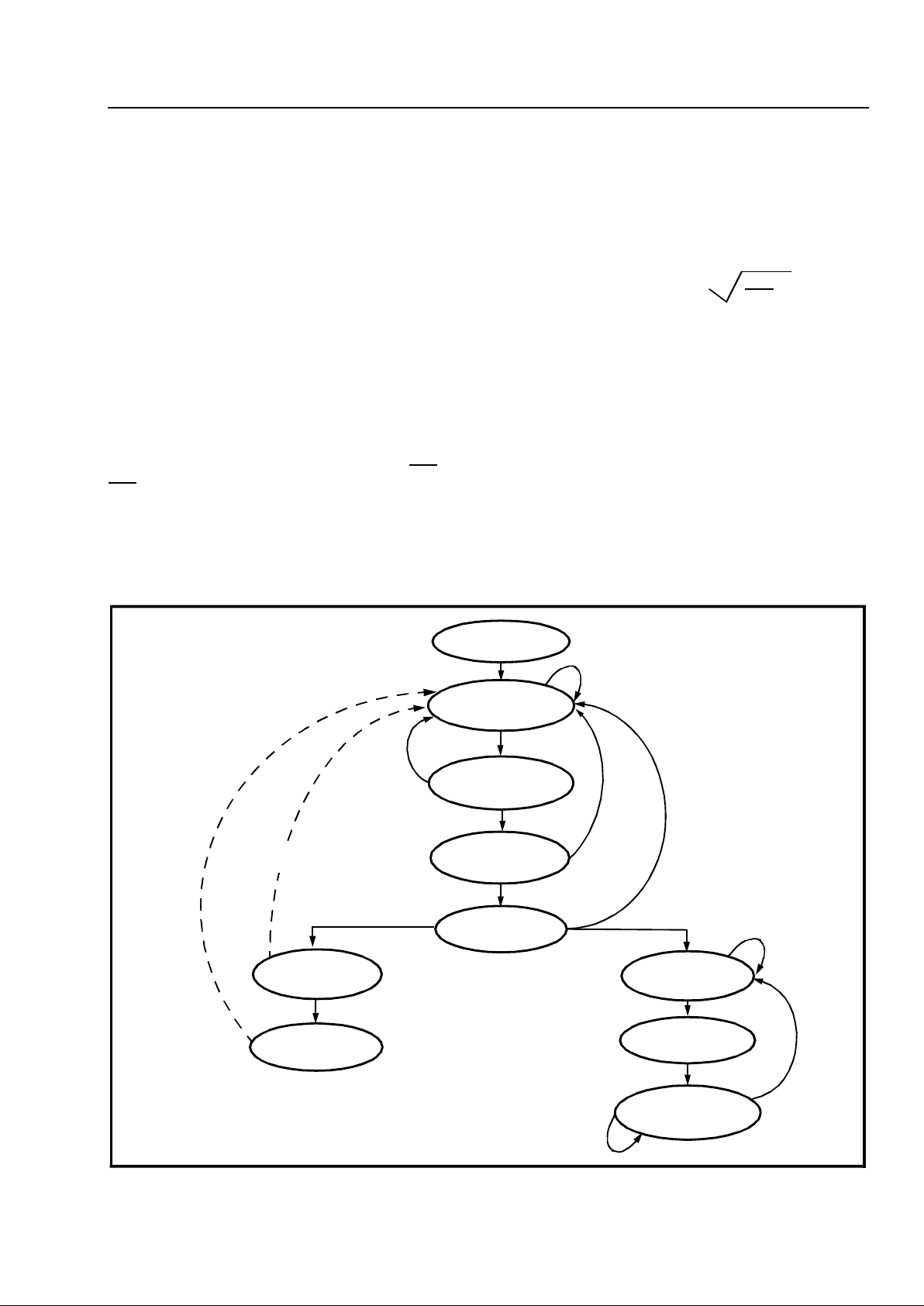
Framing Algorithms
There are three distinct framers within the
MH89790B. These include a frame alignment signal
framer, a multiframe framer and a CRC framer.
Figure 12 shows the state diagram of the framing
algorithms. The dotted lines show optional feat ures
which are enabled in the maintenance mode, that is
selected by setting Maint bit of the Master Control
Word 3 to “1”.
The frame synchronization circuit searches for the
first frame alignment signal within the bit stream.
Once detected, the frame counters are set to find the
non-frame alignment signal. If bit 2 of the non-frame
alignment signal is not one, a new search is initiated,
else the framer will monitor for the frame alignment
in the next frame. If the frame alignment signal is
found, the device immediately declares frame
synchronization.
The multiframe synchronization algorithm is
dependent upon the state of frame alignment framer.
The multiframe framer will not initiate a search for
multiframe synchronization until frame sync is
achieved. Multiframe synchronization will be
declared on the first occurrence of four consecutive
zeros in the higher order quartet of channel 16.
Once multiframe synchronization is achieved, the
framer will only go out of synchronization after
detection of two errors in the multiframe signal or
loss of frame alignment synchronization.
The CRC synchronization algorithm is also
dependent on the state of the frame alignment
Page 15
4-201
Preliminary Information MH89790B
framer, but is independent of the multiframe
synchronization. The CRC framer will not initiate a
search for CRC framing signal until frame alignment
synchronization is achieved. Once frame alignment
synchronization is acquired, the CRC framer must
find two framing signals in bit 1 of the non-frame
alignment signal. Upon detection of the second CRC
framing signal the MH89790B will immediately go
into CRC synchronization. When maintenance
feature is enabled (maint bit = 1) the CRC framer will
force a complet e reframe of the device if CRC frame
synchronization is not found within 8 ms or more
than 914 CRC errors occur per second.
Bipolar Line R ece iver
The MH89790B receiver interfaces to the
transmission line through a pulse transformer which
splits the received AMI line signal into RxA
and
RxB
. These two signals are combined by an
internal NAND gate to form a new signal, which
represents received data. The received data is
clocked into the chip on the falling edge of E2o.
Figure 28 shows the functional timing of the bipolar
receiver.
Input impedance seen by the transmission line is
about 75 ohms, (transformer ratio 1:1:1 with
center-tap grounded) as required by G.703 for
coaxial cable. Attenuation of the transmission line
shall not exceed 6dB (at 1024 kHz) and attenuation
characteristics shall be close to the “square root of
F”.
AF [dB] = AF
ref
[dB] *
where
:
AF - attenuation at frequency f in dB
AF
ref
- attenuation at frequency f
ref
in dB (in th is
case 6 dB)
f
ref
- reference frequency (in this case 1024
kHz)
f - frequency in kHz
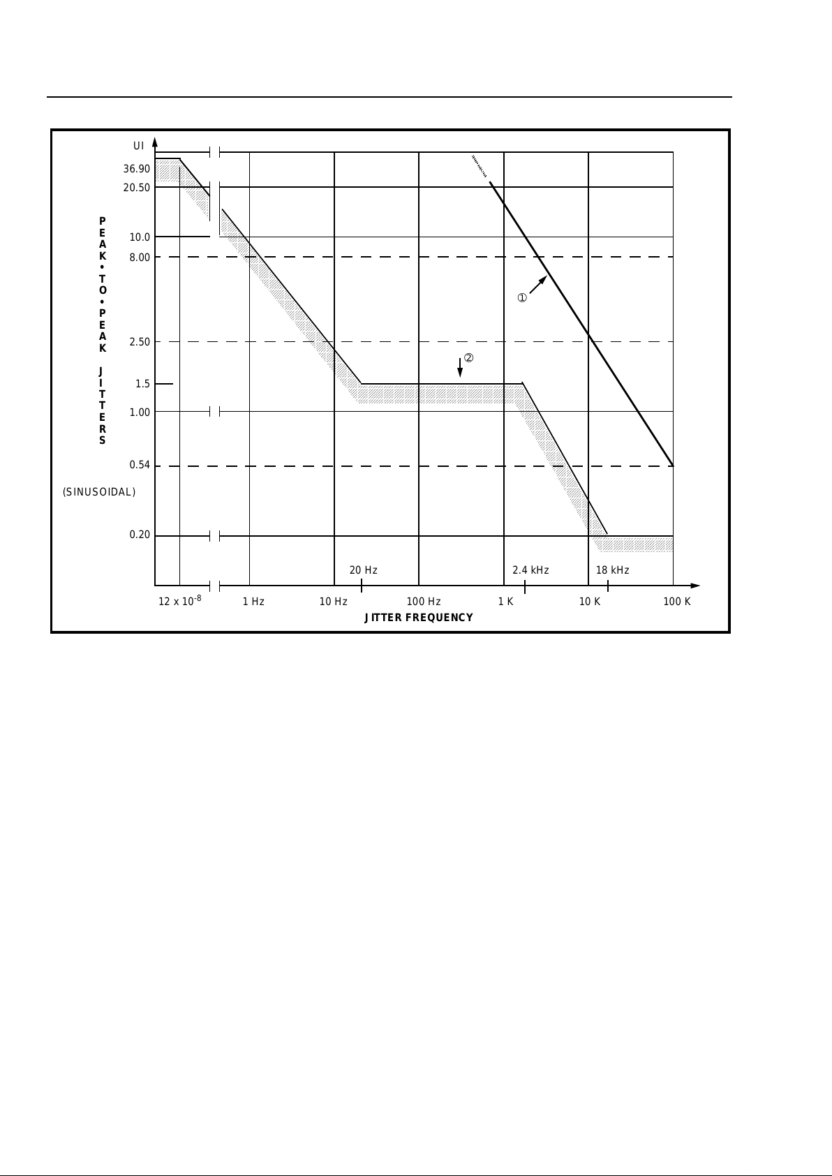
Input jitter tolerance of the MH89790B exceeds
minimum jitter tolerance as specified in CCITT I.431
and G.823 (see Figure 13).
f
f
ref
Figure 12 - Synchronization State Diagram
out of
synchronization
search for frame
alignment
signal
verify bit 2 of non-
frame alignment
signal
verify second
occurrence of frame
alig nm ent sign al
find two CRC
frame alignment
CRC synchronization
acquired
search for
mul tiframe al ign-
ment si gn al
multiframe synchro -
nization acquired
check for two errore d
multiframe alignment
signals
No
No
Yes
Yes
Yes
Yes
Yes
Yes
No
# of consecutive incorrect
frame alignment signals = 3
time out > 8m s
No
- - - - -
Only if the
mainte na n ce
option is
selected
signals
No
number of C RC
errors > 914/s
frame s ynchroni-
zation acquire d
Page 16
4-202
MH89790B Preliminary Information
Bipolar Line Transmitter
The MH89790B provides two open collector drivers,
OUTA and OUTB. These outputs are suitable for
driving a center-tapped pulse transformer. Figure 29
illustrates how the two outputs combine to create
opposite polarities of the AMI line code. Each output
steers the transformer into producing a pulse of the
opposite polarity.
Clock Extracto r
The MH89790B contains a clock extraction circuit
that generates the E2o clock from the received dat a.
This clock is used to latch received data. The falling
edge of E2o is approximately aligned with the center
of the received data pulse. Alignment between these
signals can be disrupted by jitter and wander on the
received signal. Maximum tolerance of the
MH89790B to the input jitter is shown in Figure 13
relative to minimum jitter tolerance specified in
G.823 and I.431.
The extracted 8 kHz output (E8Ko) is derived from
E2o clock by dividing it by 256. It can be used by an
external phase-locked loop to generate the system
clock and frame pulse that is synchronized to the
network (see Figure 15).
Figure 13 - Input Jitter Tolerance of MH89790B
➀ - Maximum j itt er t ol er a nc e of rec eiver
➁ - Minimum jitter to le rance spec ifi ed by G.823 an d I.431
AAAA
AAAA
AAAA
AAAA
AAAA
AAAA
AAAA
AAAA
AAAA
AAAA
AAAA
AAAA
AAAA
AAAA
AAAA
AAAA
AAAA
AAAA
AAAA
AAAA
AAAA
AAAA
AAAA
AAAA
AAAA
AAAA
AAAA
AAAA
AAAA
AAAA
AAAA
AAAA
AAAA
AAAA
AAAA
AAAA
AAAA
AAAA
AAAA
AAAA
AAAA
AAAA
AAAA
AAAA
AAAA
AAAA
AAAA
AAAA
AAAA
AAAA
AAAA
AAAA
AAAA
AAAA
AAAA
AAAA
AAAA
AAAA
AAAA
AAAA
AAAA
AAAA
AAAA
AAAA
AAAA
AAAA
AAAA
AAAA
AAAA
AAAA
AAAA
AAAA
AAAA
AAAA
AAAA
AAAA
AAAA
AAAA
AAAA
AAAA
AAAA
AAAA
AAAA
AAAA
AAAA
AAAA
AAAA
AAAA
AAAA
AAAA
AAAA
AAAA
AAAA
AAAA
AAAA
AAAA
AAAA
AAAA
AAAA
AAAA
AAAA
AAAA
AAAA
AAAA
AAAA
AAAA
AAAA
AAAA
AAAA
AAAA
AAAA
AAAA
AAAA
AAAA
AAAA
AAAA
AAAA
AAAA
AAAA
AAAA
AAAA
AAAA
AAAA
AAAA
AAAA
AAAA
AAAA
AAAA
AAAA
AAAA
AAAA
AAAA
AAAA
AAAA
AAAA
AAAA
AAAA
AAAA
AAAA
AAAA
AAAA
AAAA
AAAA
AAAA
AAAA
AAAA
AAAA
AAAA
AAAA
AAAA
AAAA
AAAA
AAAA
AAAA
AAAA
AAAA
AAAA
AAAA
AAAA
AAAA
AAAA
AAAA
AAAA
AAAA
AAAA
AAAA
AAAA
AAAA
AAAA
AAAA
AAAA
AAAA
AAAA
AAAA
AAAA
AAAA
AAAA
AAAA
AAAA
AAAA
AAAA
AAAA
AAAA
AAAA
AAAA
AAAA
AAAA
AAAA
AAAA
AAAA
AAAA
AAAA
AAAA
AAAA
AAAA
AAAA
AAAA
AAAA
AAAA
AAAA
AAAA
AAAA
AAAA
AAAA
AAAA
AAAA
AAAA
AAAA
AAAA
AAAA
AAAA
AAAA
AAAA
AAAA
AAAA
AAAA
AAAA
AAAA
AAAA
AAAA
AAAA
AAAA
AAAA
AAAA
AAAA
AAAA
AAAA
AAAA
AAAA
AAAA
AAAA
AAAA
AAAA
AAAA
AAAA
AAAA
AAAA
AAAA
AAAA
AAAA
AAAA
AAAA
AAAA
AAAA
AAAA
AAAA
AAAA
AAAA
AAAA
AAAA
AAAA
AAAA
AAAA
AAAA
AAAA
AAAA
AAAA
AAAA
AAAA
AAAA
AAAA
AAAA
AAAA
AAAA
AAAA
AAAA
AAAA
AAAA
AAAA
AAAA
AAAA
AAAA
AAAA
AAAA
AAAA
AAAA
AAAA
AAAA
AAAA
AAAA
AAAA
AAAA
AAAA
AAAA
AAAA
AAAA
AAAA
AAAA
AAAA
AAAA
AAAA
AAAA
AAAA
AAAA
AAAA
AAAA
AAAA
AAAA
AAAA
AAAA
AAAA
AAAA
AAAA
AAAA
AAAA
AAAA
AAAA
AAAA
AAAA
AAAA
AAAA
AAAA
AAAA
AAAA
AAAA
AAAA
AAAA
AAAA
AAAA
AAAA
AAAA
AAAA
AAAA
AAAA
AAAA
AAAA
AAAA
AAAA
AAAA
AAAA
AAAA
AAAA
AAAA
AAAA
AAAA
AAAA
AAAA
AAAA
AAAA
AAAA
AAAA
AAAA
AAAA
AAAA
AAAA
AAAA
AAAA
AAAA
AAAA
AAAA
AAAA
AAAA
AAAA
AAAA
AAAA
AAAA
AAAA
AAAA
AAAA
AAAA
AAAA
AAAA
AAAA
AAAA
AAAA
AAAA
AAAA
AAAA
AAAA
AAAA
AAAA
AAAA
AAAA
AAAA
AAAA
AAAA
AAAA
AAAA
AAAA
AAAA
AAAA
AAAA
AAAA
AAAA
AAAA
AAAA
AAAA
AAAA
AAAA
AAAA
AAAA
AAAA
AAAA
AAAA
AAAA
AAAA
AAAA
AAAA
AAAA
AAAA
AAAA
AAAA
AAAA
AAAA
AAAA
AAAA
AAAA
AAAA
AAAA
AAAA
AAAA
AAAA
AAAA
AAAA
AAAA
AAAA
AAAA
AAAA
AAAA
AAAA
AAAA
AAAA
AAAA
AAAA
AAAA
AAAA
AAAA
AAAA
AAAA
AAAA
AAAA
AAAA
AAAA
AAAA
AAAA
AAAA
AAAA
AAAA
AAAA
AAAA
AAAA
AAAA
AAAA
AAAA
AAAA
AAAA
AAAA
AAAA
AAAA
AAAA
AAAA
AAAA
AAAA
AAAA
AAAA
AAAA
AAAA
AAAA
AAAA
AAAA
AAAA
AAAA
AAAA
AAAA
AAAA
AAAA
AAAA
AAAA
AAAA
AAAA
AAAA
AAAA
AAAA
AAAA
AAAA
AAAA
AAAA
AAAA
AAAA
AAAA
AAAA
AAAA
AAAA
AAAA
AAAA
AAAA
AAAA
AAAA
AAAA
AAAA
AAAA
AAAA
AAAA
AAAA
AAAA
AAAA
AAAA
AAAA
AAAA
AAAA
AAAA
AAAA
AAAA
AAAA
AAAA
AAAA
AAAA
AAAA
AAAA
AAAA
AAAA
AAAA
AAAA
AAAA
AAAA
AAAA
AAAA
AAAA
AAAA
AAAA
AAAA
AAAA
AAAA
AAAA
AAAA
AAAA
AAAA
AAAA
AAAA
AAAA
AAAA
AAAA
AAAA
AAAA
AAAA
AAAA
AAAA
AAAA
AAAA
AAAA
AAAA
AAAA
AAAA
AAAA
AAAA
AAAA
AAAA
AAAA
AAAA
AAAA
AAAA
AAAA
AAAA
AAAA
AAAA
AAAA
AAAA
AAAA
AAAA
AAAA
AAAA
AAAA
AAAA
AAAA
AAAA
AAAA
AAAA
AAAA
AAAA
AAAA
AAAA
AAAA
AAAA
AAAA
AAAA
AAAA
AAAA
AAAA
AAAA
AAAA
AAAA
AAAA
AAAA
AAAA
AAAA
AAAA
AAAA
AAAA
AAAA
AAAA
AAAA
AAAA
AAAA
AAAA
AAAA
AAAA
AAAA
AAAA
AAAA
AAAA
AAAA
AAAA
AAAA
AAAA
AAAA
AAAA
AAAA
AAAA
AAAA
AAAA
AAAA
AAAA
AAAA
AAAA
AAAA
AAAA
AAAA
AAAA
AAAA
AAAA
AAAA
AAAA
AAAA
AAAA
AAAA
AAAA
AAAA
AAAA
AAAA
AAAA
AAAA
AAAA
AAAA
AAAA
AAAA
AAAA
AAAA
AAAA
AAAA
AAAA
AAAA
AAAA
AAAA
AAAA
AAAA
AAAA
AAAA
AAAA
AAAA
AAAA
AAAA
AAAA
AAAA
AAAA
AAAA
AAAA
AAAA
AAAA
AAAA
AAAA
AAAA
AAAA
AAAA
AAAA
AAAA
AAAA
AAAA
AAAA
AAAA
AAAA
AAAA
AAAA
AAAA
AAAA
AAAA
AAAA
AAAA
AAAA
AAAA
AAAA
AAAA
AAAA
AAAA
AAAA
AAAA
AAAA
AAAA
AAAA
AAAA
AAAA
AAAA
AAAA
AAAA
AAAA
AAAA
AAAA
AAAA
AAAA
AAAA
AAAA
AAAA
AAAA
AAAA
AAAA
AAAA
AAAA
AAAA
AAAA
AAAA
AAAA
AAAA
AAAA
AAAA
AAAA
AAAA
AAAA
AAAA
AAAA
AAAA
AAAA
AAAA
AAAA
AAAA
AAAA
AAAA
AAAA
AAAA
AAAA
AAAA
AAAA
AAAA
AAAA
AAAA
AAAA
AAAA
AAAA
AAAA
AAAA
AAAA
AAAA
AAAA
AAAA
AAAA
AAAA
AAAA
AAAA
AAAA
AAAA
AAAA
AAAA
AAAA
AAAA
AAAA
AAAA
AAAA
AAAA
AAAA
AAAA
AAAA
AAAA
AAAA
AAAA
AAAA
AAAA
AAAA
AAAA
AAAA
AAAA
AAAA
AAAA
AAAA
AAAA
AAAA
AAAA
AAAA
AAAA
AAAA
AAAA
AAAA
AAAA
AAAA
AAAA
AAAA
AAAA
AAAA
AAAA
AAAA
AAAA
AAAA
AAAA
AAAA
AAAA
AAAA
AAAA
AAAA
AAAA
AAAA
AAAA
AAAA
AAAA
AAAA
AAAA
AAAA
AAAA
AAAA
AAAA
AAAA
AAAA
AAAA
AAAA
AAAA
AAAA
AAAA
AAAA
AAAA
AAAA
AAAA
AAAA
AAAA
AAAA
AAAA
AAAA
AAAA
AAAA
AAAA
AAAA
AAAA
AAAA
AAAA
AAAA
AAAA
AAAA
AAAA
AAAA
AAAA
AAAA
AAAA
AAAA
AAAA
AAAA
AAAA
AAAA
AAAA
AAAA
AAAA
AAAA
AAAA
AAAA
AAAA
AAAA
AAAA
AAAA
AAAA
AAAA
AAAA
AAAA
AAAA
AAAA
AAAA
AAAA
AAAA
AAAA
AAAA
AAAA
AAAA
AAAA
AAAA
AAAA
AAAA
AAAA
AAAA
AAAA
AAAA
AAAA
AAAA
AAAA
AAAA
AAAA
AAAA
AAAA
AAAA
AAAA
AAAA
AAAA
AAAA
AAAA
AAAA
AAAA
AAAA
AAAA
AAAA
AAAA
AAAA
AAAA
AAAA
AAAA
AAAA
AAAA
AAAA
AAAA
AAAA
AAAA
AAAA
AAAA
AAAA
AAAA
AAAA
AAAA
AAAA
AAAA
AAAA
AAAA
AAAA
AAAA
AAAA
AAAA
AAAA
AAAA
AAAA
AAAA
AAAA
AAAA
AAAA
AAAA
AAAA
AAAA
AAAA
AAAA
AAAA
AAAA
AAAA
AAAA
AAAA
AAAA
AAAA
AAAA
AAAA
AAAA
AAAA
AAAA
AAAA
AAAA
AAAA
AAAA
AAAA
AAAA
AAAA
AAAA
AAAA
AAAA
AAAA
AAAA
AAAA
AAAA
AAAA
AAAA
AAAA
AAAA
AAAA
AAAA
AAAA
AAAA
AAAA
AAAA
AAAA
AAAA
AAAA
AAAA
AAAA
AAAA
AAAA
AAAA
AAAA
AAAA
AAAA
AAAA
AAAA
AAAA
AAAA
AAAA
AAAA
AAAA
AAAA
AAAA
AAAA
AAAA
AAAA
AAAA
AAAA
AAAA
AAAA
AAAA
AAAA
AAAA
AAAA
AAAA
AAAA
AAAA
AAAA
AAAA
AAAA
AAAA
AAAA
AAAA
AAAA
AAAA
AAAA
AAAA
AAAA
AAAA
AAAA
AAAA
AAAA
AAAA
AAAA
AAAA
AAAA
AAAA
AAAA
AAAA
AAAA
AAAA
AAAA
AAAA
AAAA
AAAA
AAAA
AAAA
AAAA
AAAA
AAAA
AAAA
AAAA
AAAA
AAAA
AAAA
AAAA
AAAA
AAAA
AAAA
AAAA
AAAA
AAAA
AAAA
AAAA
AAAA
AAAA
AAAA
AAAA
AAAA
AAAA
AAAA
AAAA
AAAA
AAAA
AAAA
AAAA
AAAA
AAAA
AAAA
AAAA
AAAA
AAAA
AAAA
AAAA
AAAA
AAAA
AAAA
AAAA
AAAA
AAAA
AAAA
AAAA
AAAA
AAAA
AAAA
AAAA
AAAA
AAAA
AAAA
AAAA
AAAA
AAAA
AAAA
AAAA
AAAA
AAAA
AAAA
AAAA
AAAA
AAAA
AAAA
AAAA
AAAA
AAAA
AAAA
AAAA
AAAA
AAAA
AAAA
AAAA
AAAA
AAAA
AAAA
AAAA
AAAA
AAAA
AAAA
AAAA
AAAA
AAAA
AAAA
AAAA
AAAA
AAAA
AAAA
AAAA
AAAA
AAAA
AAAA
AAAA
AAAA
AAAA
AAAA
AAAA
AAAA
AAAA
AAAA
AAAA
AAAA
AAAA
AAAA
AAAA
AAAA
AAAA
AAAA
AAAA
AAAA
AAAA
AAAA
AAAA
AAAA
AAAA
AAAA
AAAA
AAAA
AAAA
AAAA
AAAA
AAAA
AAAA
AAAA
AAAA
AAAA
AAAA
AAAA
AAAA
AAAA
AAAA
AAAA
AAAA
AAAA
AAAA
AAAA
AAAA
AAAA
AAAA
AAAA
AAAA
AAAA
AAAA
AAAA
AAAA
AAAA
AAAA
AAAA
AAAA
AAAA
AAAA
AAAA
AAAA
AAAA
AAAA
AAAA
AAAA
AAAA
AAAA
AAAA
AAAA
AAAA
AAAA
AAAA
AAAA
AAAA
AAAA
AAAA
AAAA
AAAA
AAAA
AAAA
AAAA
AAAA
AAAA
AAAA
AAAA
AAAA
AAAA
AAAA
AAAA
AAAA
AAAA
AAAA
AAAA
AAAA
AAAA
AAAA
AAAA
AAAA
AAAA
AAAA
AAAA
AAAA
AAAA
AAAA
AAAA
AAAA
AAAA
AAAA
AAAA
AAAA
AAAA
AAAA
AAAA
AAAA
AAAA
AAAA
AAAA
AAAA
AAAA
AAAA
AAAA
AAAA
AAAA
AAAA
AAAA
AAAA
AAAA
AAAA
AAAA
AAAA
AAAA
AAAA
AAAA
AAAA
AAAA
AAAA
AAAA
AAAA
AAAA
AAAA
AAAA
AAAA
AAAA
AAAA
AAAA
AAAA
AAAA
AAAA
AAAA
AAAA
AAAA
AAAA
AAAA
AAAA
AAAA
AAAA
AAAA
AAAA
AAAA
AAAA
AAAA
AAAA
AAAA
AAAA
AAAA
AAAA
AAAA
AAAA
AAAA
AAAA
AAAA
AAAA
AAAA
AAAA
AAAA
AAAA
AAAA
AAAA
AAAA
AAAA
AAAA
AAAA
AAAA
AAAA
AAAA
AAAA
AAAA
AAAA
AAAA
AAAA
AAAA
AAAA
AAAA
AAAA
AAAA
AAAA
AAAA
AAAA
AAAA
AAAA
AAAA
AAAA
AAAA
AAAA
AAAA
AAAA
AAAA
AAAA
AAAA
AAAA
AAAA
AAAA
AAAA
AAAA
AAAA
AAAA
AAAA
AAAA
AAAA
AAAA
AAAA
AAAA
AAAA
AAAA
AAAA
AAAA
AAAA
AAAA
AAAA
AAAA
AAAA
AAAA
AAAA
AAAA
AAAA
AAAA
AAAA
AAAA
AAAA
AAAA
AAAA
AAAA
AAAA
AAAA
AAAA
AAAA
AAAA
AAAA
AAAA
AAAA
AAAA
AAAA
AAAA
AAAA
AAAA
AAAA
AAAA
AAAA
AAAA
AAAA
AAAA
AAAA
AAAA
AAAA
AAAA
AAAA
20 Hz 2.4 kHz 18 kHz
12 x 10
-8
1 Hz 10 Hz 100 Hz 1 K 10 K 100 K
36.90
20.50
10.0
8.00
2.50
1.5
1.00
0.54
(SINUSOIDAL)
0.20
UI
P
E
A
K
•
T
O
•
P
E
A
K
J
I
T
T
E
R
S
JITTER FREQUENCY
AAAA
AAAA
AAAA
AAAA
AAAA
AAAA
AAAA
AAAA
AAAA
AAAA
AAAA
AAAA
AAAA
AAAA
AAAA
AAAA
AAAA
AAAA
AAAA
AAAA
AAAA
AAAA
➀
➁
Page 17
4-203
Preliminary Information MH89790B
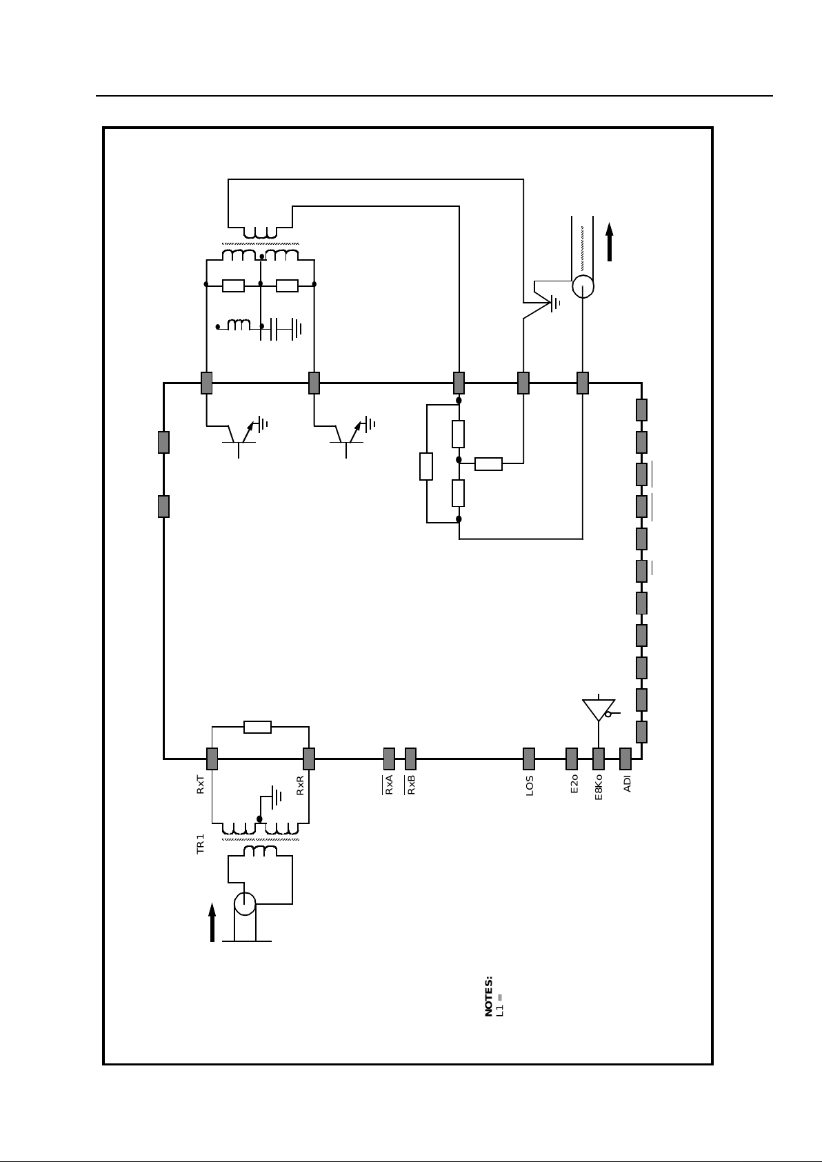
Figure 14 - Interf acing the M H8979 0B to the 75 Ω Coaxial Cable
•••
•
•
•
•
•
•
•
TR1 RxT
RxR
RxA
RxB
LOS
E2o
E8Ko
ADI
NOTES:
L1 = 33µH 130 mA
C1 = 0.47µF 20% Cera mic
R1, R2 = 887Ω 1%
TR2 = Filtran* Part #TFS2915-5
(+5V Su pply)
Filtran* Part #TFS2915-4
(+12V Supply)
TR1= Filtran* Part #TFS2574-4
*
Filtran Ltd.
229 Colonade Road
Nepean, Ontario
Canada, K2E 7K3
Telephone: (613) 226-1626
DSTo DSTi CSTo CSTi0 CSTi1 F0i
C2i RxMF TxMF XCtl XSt
VSS VDD
2N2369
2N2369
75Ω
75Ω
75Ω
75Ω
OUTA
OUTB
+5V
(+12V)
L1
C1
R1
R2
TR2
PADi
TxG
PADo
319Ω
MH89790B
Note:
Variations in the transformer supply
voltage will af fect the transmit pulse amp li tude (maximum tolerance is ±5%).
Page 18
4-204
MH89790B Preliminary Information
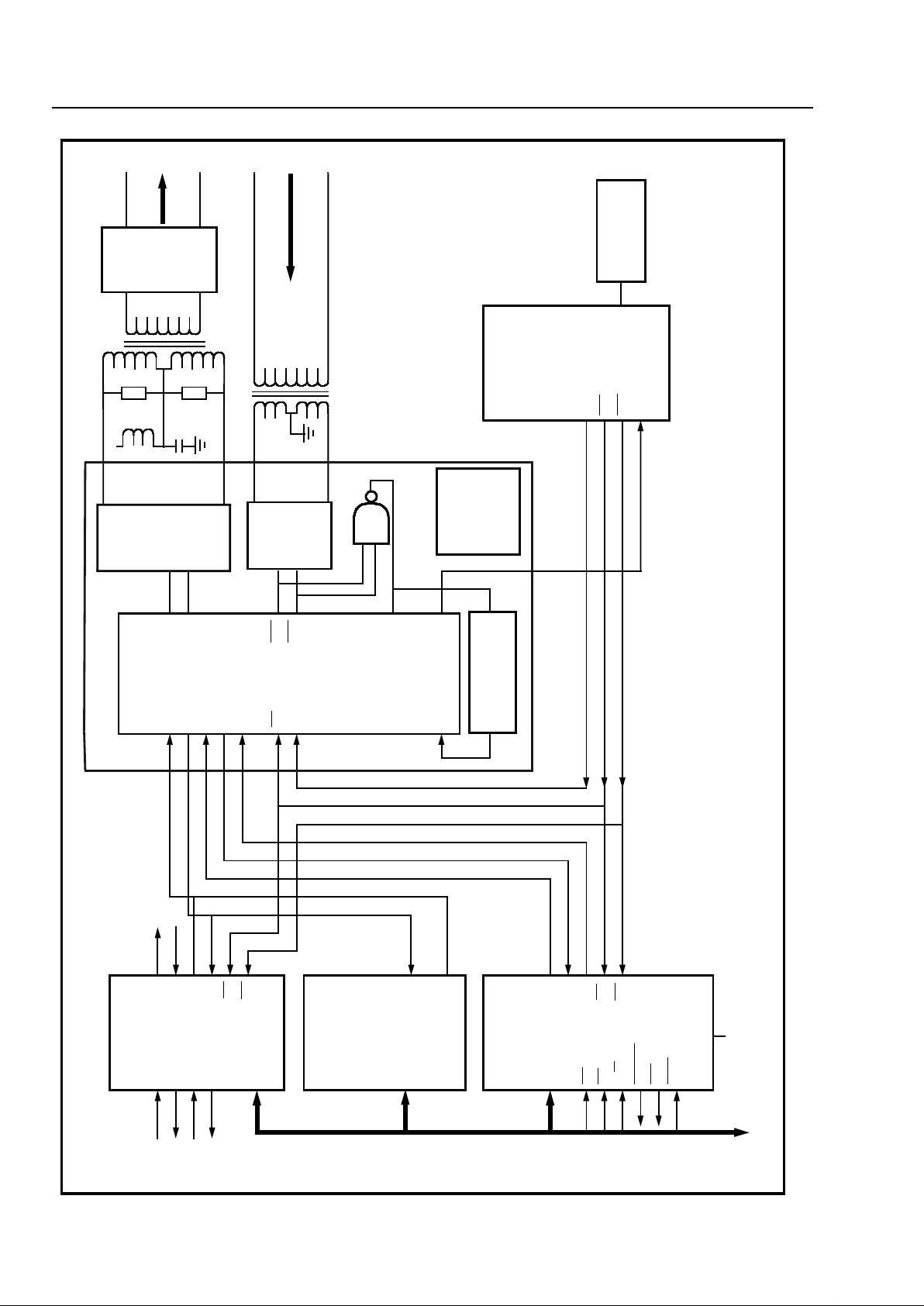
Figure 15 - Ty pical Primary Rate ISDN Application (interfacing to 120Ω Twisted Pair)
MT8980
Switch
Matrix
STo0
STi0
F0i
C4i
MT8952
D-Channel
Protocol
Controller
CDSTi
CDSTo
MT8920B
(Mode 1)
STo0
STi0
STo1
F0i
C4i
CSDSR/W
DTACK
IRQ
IACK
MMS
+5V
Clock
Extractor
•
NOTES:
L1 = 33µH 130 MA
C1 = 0.47µF 20% Ceramic
R1, R2 = 909Ω 1%
TR2 = Filtran* Part #TFS2915-5 (+5V Supply)
Filtran* Part #TFS2915-4 (+12V Supply)
TR1 = Filtran* Part #TFS2574-4
*
Filtran Ltd .
229 Colonnade Road
Nepean, Ontario
Canada, K2E 7K3
Teleph on e: (613) 226-162 6
MH89790B
MT8979
DSTi
DSTo
CSTi0
CSTo
CSTi1
F0i
C2i
TxA
TxB
RxA
RxB
RxD
E2i
E8Ko
Tx
Line
Driver
Rx
Line
Receiver
75Ω
Line
Matching
Pad
+5V
(+12V)
R1
C1
R2
TR1
TR2
120Ω
Line
Matchi ng
Pad or
Equaliz e r
Twisted
Pair
Twisted Pair
MT8941
(Note 1)
C2o
F0b
C4b
C8Ko
16.384 MH z
Osc.
Note 1: Using the MT8941 may not me et some
international standards for jitter
performance. In cases where strict output
jitter specification must be met, custom PLL
may be required.
OUTA
OUTB
RxT
RxR
M
I
C
R
O
P
ROC
ESS
O
R
I
N
T
E
RFA
C
E
•
•
•
•
•
•
•
•
•
•
•
•
Page 19
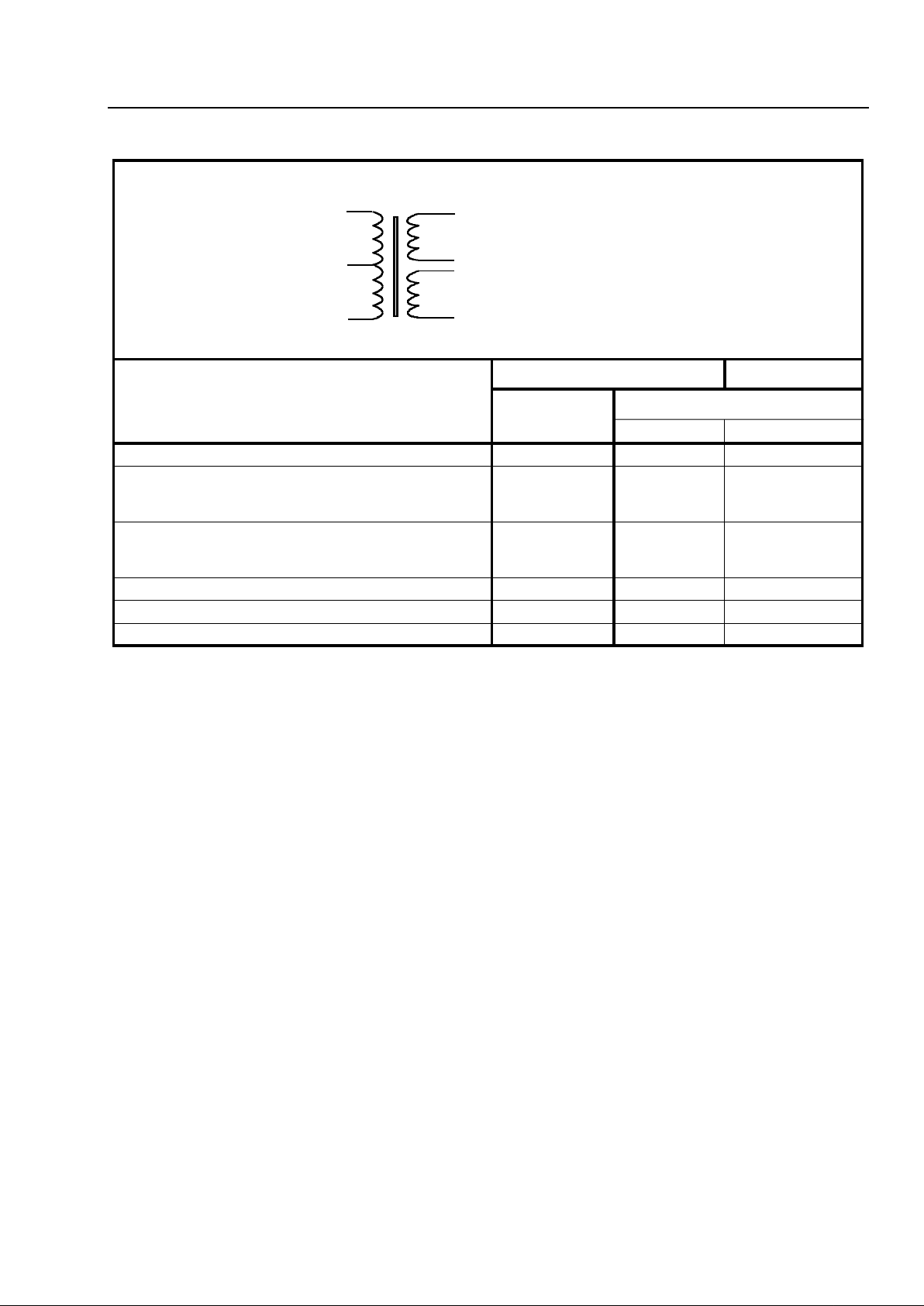
4-205
Preliminary Information MH89790B
Ta ble 18. Typical Parameters of the Input and Output Transformers
Parameter
(Units)
Throug h Hole Units
TFS 2574-4
TFS 2915
-4 -5
Transformer Ty pe input output output
Inductance (mH)
(COM1-75Ω)
(COM1-120Ω)
>1.2
>1.9
0.49
0.81
>1
>1.5
Turns Ratio
(COM1-75Ω):(A-F1):(B- F2)
(COM1-120Ω):(COM1-75Ω)
1:1:1
1•26:1
0•4:1:1
1•28:1
1•12:1:1
1•22:1
Line Impedance (Ω) 75/120 75/120 75/120
Operational Voltage (Volts) - +12 +5
Dielectric Strength (Vrms) 1500 1500 1500
Line Side
System Side
•
•
•
O
O
O
O
O
O
COM1
120Ω
A
F2
F1
B
O
75Ω
Applications
ISDN Primary Rat e User Ne twork In terface
Typical examples of primary rate interfaces are high
capacity links from a PBX to a Central Office
Exchange or multiple links between PBX’s in a large
private network. With the advent of Integrated
Services Digital Networks (ISDN) a limited set of
network interfaces is specified to allow equipment
from different vendors to operate in the network.
The MH89790B conforms to the ISDN S/T Primary
Rate refer ence point standa rd, which calls for 30 B
channels (64 kbit/s) and one D channel (64 kbit/s).
Figure 15 illustrates a typical application of the
MH89790B in an ISDN environment.
Three types of information are passed through serial
busses of the MH89790B:
USER DATA
- The data streams of the MH89790B
are shown connected to the MT8980 Digital
Crosspoint Switch. This allows voice and data
channels to be switched dynamically within the
system.
SIGNALLING -
Signalling information on the ISDN
primary rate interface is carried over the D-channel
using LAPD procedures. The ISDN D-channel is
created by placing the MH89790B in Common
Channel Signalling mode. The D-channel is tapped
off from the ST-BUS and connected to the MT8952
Protocoller Controller. It receives and transmits data
packets serially, in accordance with LAPD protocol
requirements.
CONTROL -
The MT8920B (STPA) provides
microprocessor access to directly control the
MH89790B through its transmit and receive dual port
RAMs. S ta tu s in fo rm a ti on c a n g ene ra te in te r ru p ts to
notify the system in case of slips, loss of
synchron iz a tion , alarms, vio l at i ons, etc.
Interfacing to the Coaxial Cable Transmission
Line
Reliable operation of the CEPT link is directly related
to the type of transmission medium and method of
interfacing. Coaxial cables provide excellent
transmission mediums if used properly. One of the
most important things to remember is that the
receive end of the cable must not be connected to
ground, as shown in Figure 16. If both ends are
Page 20
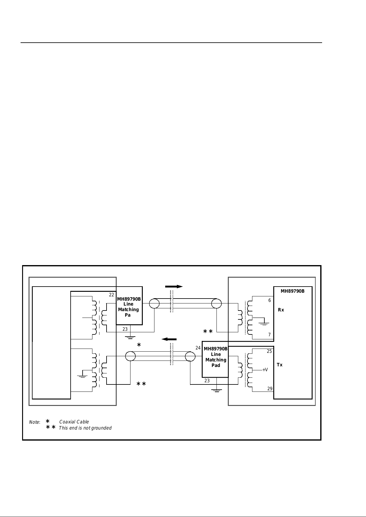
4-206
MH89790B Preliminary Information
connected to the ground, uncontrolled current will
flow through the shield of the cable and interfere with
the transmitted signal.
Magnetics Information
Table 18 provides typical electrical parameters for
suitable input and output transformers. For
supporting initial design activities, Mitel
Semiconductor has available CEPT MH89790B
Ancilliary Component Kits which contains input and
output transformers. Alternatively, they are available
directly fro m the followin g m a nu fa c tu re r:
Filtran Ltd.
229 Colonnade Road
Nepean, Ontario
Canada K2E 7K3
Telephone: 613-226-1626.
Figure 16 - Grounding Method of the Outer Conductor to the Coaxial Cable
MH89790B
Line
Matching
Pad
MH89790B
Rx
Tx
6
7
25
29
+V
* *
24
23
23
* *
* *
*
*
Note
:
Coaxial Cable
Thi s end is not g ro unde d
22
MH89790B
Line
Matching
Pad
25
29
6
7
MH8979 0B
Tx
Rx
+V
22
•
•
•
•
•
•
•
•
•
•
24
Page 21

4-207
Preliminary Information MH89790B
* Exceedi ng these values ma y cause perm anen t damage . Functi onal operati on under the se cond itions is not impl ied.
† Timing is over recommended temperature & power supply voltages.
‡ Typical figures are at 25°C and are for design aid only: not guaranteed and not subject to prod ucti on testin g.
Absolute Maximum Rating s*
Parameter Symbol Min Max Units
1 Supply Voltage with respect to V
SS
V
DD
-0.3 7 V
2 Voltage on any pin other than supplies V
SS
-0.3 VDD+0.3 V
3 Current at any pin other than supplies 40 mA
4 Storage Temperature T
ST
-40 85 °C
5 Package Power Dissipation P 800 mW
Recommended Operating Conditions - Voltages are with respect to ground (V
SS
) unless otherwise stated.
Characteristics Sym Min Typ‡Max Units Test Conditions
1
I
n
p
u
t
s
Operating Temperature T
OP
070°C
2 Supply Voltage V
DD
4.5 5.0 5.5 V
3 Input High Voltage V
IH
2.4 V
DD
V For 400 mV noise margin
V
IH
1.2 V RxT and RxR
4 Input Low Voltage V
IL
V
SS
0.4 V For 400 mV noise margin
V
IL
0.3 V RxT and RxR
DC Electrical Characteristics - Clocked operation over recommended temperature ranges and power supply voltages.
Parameters Sym Min Typ‡Max Units Test Conditions
1
I
n
p
u
t
s
Supply Current I
DD
15 45 mA Outputs Unloaded
2 Input High Voltage V
IH
2.0 V
DD
V Digital Inputs
3 Input Low Voltage V
IL
0.0 0.8 V Digital Inputs
4 Input Leakage Current I
IL
+1+10 µA Digital Inputs VIN=0 toV
DD
5
O
u
t
p
u
t
s
Output High Voltage V
OH
2.4 V
DD
VIOL=10mA
6 Output High Leakage I
OZ
500 nA VO = 0 to V
DD
7 Output High Current I
OH
7 20 mA Source Current , VOH=2.4V
8 Output Low Voltage V
OL
V
SS
0.4 V IOL=2mA
OUTA or OUTB V
OL
0.25 V IOL=10mA
9 Output Low Current I
OL
2 10 mA S ink Current , VOL=0.4V
10 Input Impedance RxT to RxR 319 Ω
AC Electrical Characteristics† - Capacitance
Characteristics Sym Min Typ‡Max Units Test Conditions
1 Input Pin Capacitance C
I
10 pF
2 Output Pin Capacitance C
O
10 pF
Page 22
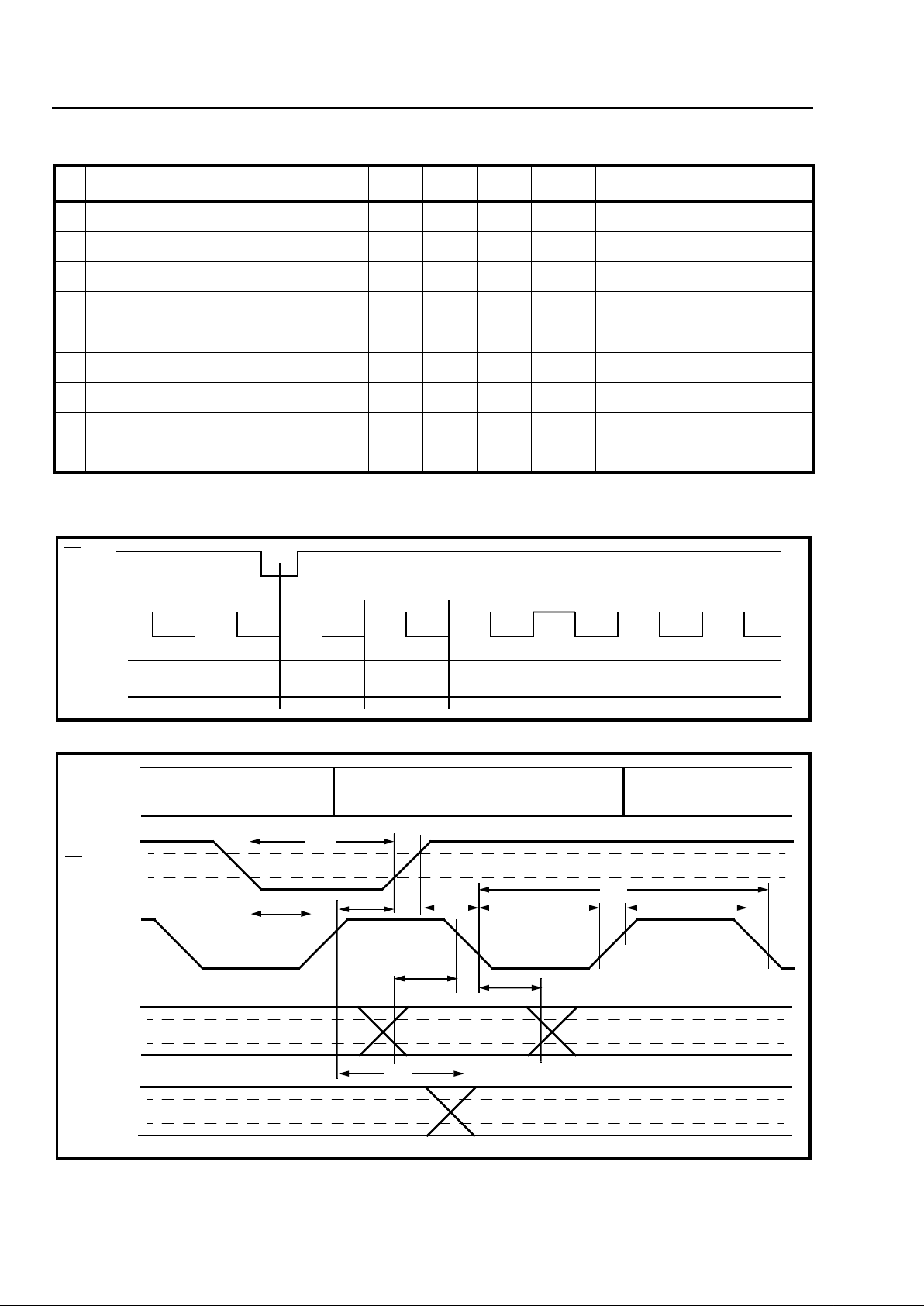
4-208
MH89790B Preliminary Information
† Characteristics are for clocked operation over the ranges of recommended opera tin g temperature and supp ly vol tag e.
‡ Typical figures are at 25°C and are for design aid only: not guaranteed and not subject to prod ucti on testin g.
Figure 17 - Clock & F rame A lign ment fo r 2048 kbit/s ST-BUS Streams
Figure 18 - Cloc k & Fra me Timing for 2 048 kb it/s S T-BUS Streams
AC Electrical Characteristics† - ST-BUS Timing ( Figures 17 and 18)
Characteristics Sym Min Typ‡Max Units Test Conditions
1 C2i Clock Period t
P20
400 488 600 ns
2 C2i Clock Width High or Low t
W20
200 244 ns t
P20
= 488 ns
3 Frame Pulse Setup Time t
FPS
50 150 ns
4 Frame Pulse Hold Time t
FPH
50 ns
5 Frame Pulse Width t
FPW
100 300 ns
6 Serial Output Delay t
SOD
125 ns 150 pF Load
7 Serial Input Setup Time t
SIS
30 ns
8 Serial Input Hold Time t
SIH
55 ns
9 Frame Pulse Setup Time 2 t
FPS2
20 ns
F0i
C2i
ST-BUS
BIT CELLS
Channel 31 Channel 0 Channel 0
Bit 0 Bit 7 Bit 6
ST-BUS
Bit Stream
Bit Cell
F0i
C2i
DSTi
or
CSTi0/1
DSTo
or
CSTo
V
IL
V
IH
V
IL
V
IH
V
IL
V
IH
V
OL
V
OH
t
FPS
t
FPH
t
FPW
t
FPS2
t
P20
t
SIS
t
W20
t
W20
t
SIH
t
SOD
Page 23
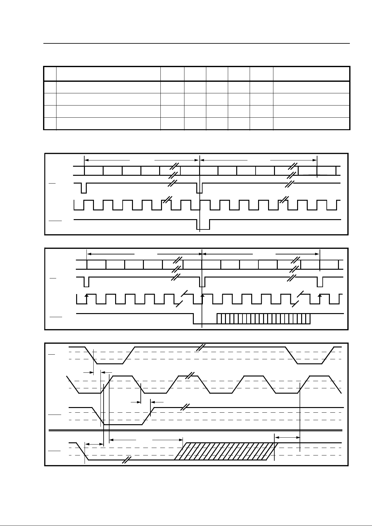
4-209
Preliminary Information MH89790B
† Characteristics are for clocked operation over the ranges of recommended opera tin g temperature and supp ly vol tag e.
‡ Typical figures are at 25°C and are for design aid only: not guaranteed and not subject to prod ucti on testin g.
*256 t
P20
- 100ns
Figure 19 - Functional Timing for Receive Multiframe Clocks
Figure 20 - Functional Timing for Transmit Multiframe Clock
Figure 21 - Clock and Frame Timing for 2048 kbit/s ST-BUS Streams
Note 1: These two signals do not have a defined phase relationship
AC Electrical Characteristics† - Multiframe Clock Timing (Figure 21)
Characteristics Sym Min Typ‡Max Units Test Conditions
1 Receive Multiframe Output Delay t
RMFD
150 ns 50pF
2 Transmit Multiframe Setup Time t
TMFS
50 ns
3 Transmit Multiframe Hold Time t
TMFH
50 * ns
4 Tx Multiframe to C2 Setup Time t
MF2S
100 ns
DSTo
Bit Cells
F0i
C2i
RxMF
Bit 7 Bit 6 Bit 5 Bit 4 Bit 0 Bit 7 Bit 6 Bit 5 Bit 4 Bit 0 Bit 7
Frame 0Frame 15
F0i
C2i
TxMF
DSTi
Bit Cells
Bit 7 Bit 6 Bit 5 Bit 4 Bit 0 Bit 7 Bit 6 Bit 5 Bit 4 Bit 0 Bit 7
Frame 0F ram e N
F0i
C2i
RxMF
(1)
TxMF
(1)
t
RMFD
t
TMFS
t
MF2S
t
TMFH
t
RMFD
Page 24
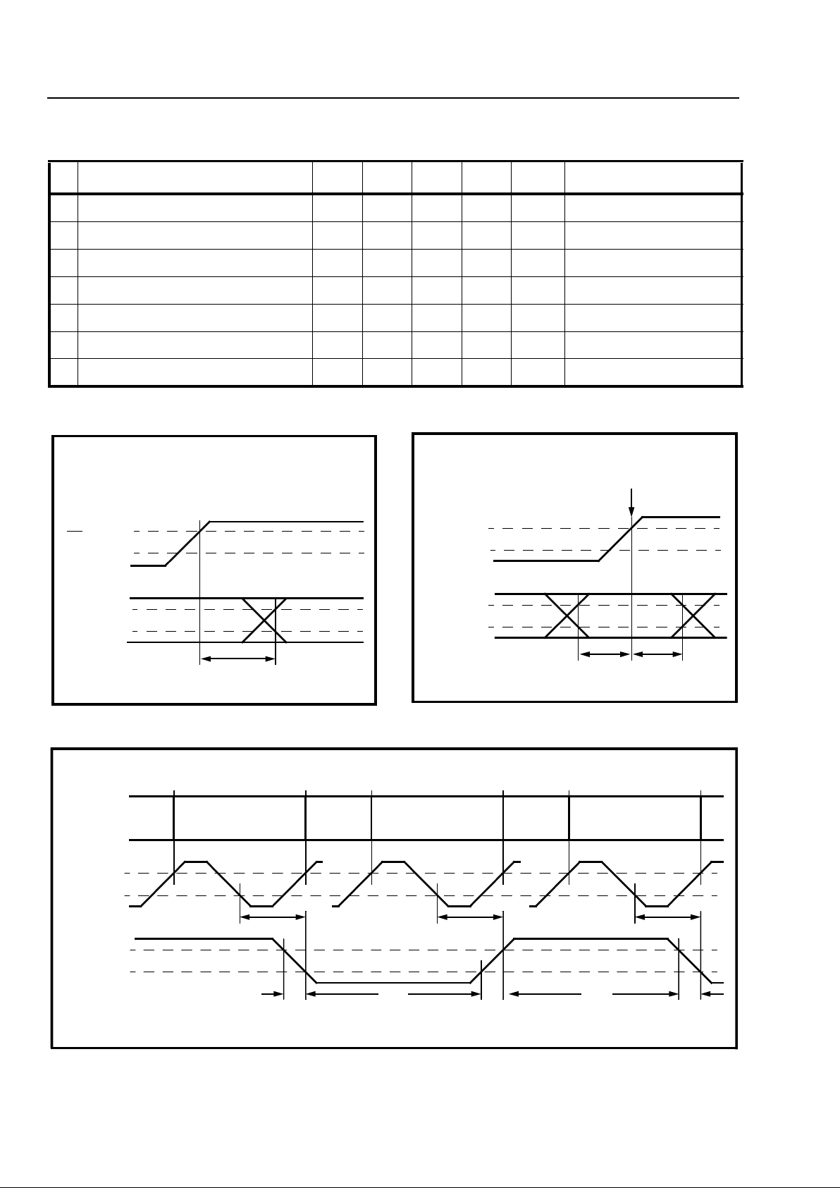
4-210
MH89790B Preliminary Information
† Characteristics are for clocked operation over the ranges of recommended opera tin g temperature and supp ly vol tag e.
‡ Typical figures are at 25°C and are for design aid only: not guaranteed and not subject to prod ucti on testin g.
AC Electrical Characteristics† - XCtl, XS and E8Ko (Figures 22, 23 and 24)
Characteristics S ym M in Typ‡Max Units Test Conditions
1 External Control Delay t
XCD
100 ns 50 pF load
2 External Status Setup Time t
XSS
50 ns
3 External Status Hold Time t
XSH
50 ns
4 E8Ko Output Delay t
8OD
150 ns 50 pF load
5 E8Ko Output Low Width t
8OL
62.5 µs 50 pF load
6 E8Ko Output High Width t
8OH
62.5 µs 50 pF load
7 E8Ko Output Transition Time t
8OT
20 ns 50 pF load
Figure 24 - E8Ko Timing
Timeslot 0
Bit 4
Timeslot 16
Bit 4
Timeslot 0
Bit 4
Received
CEPT Bits
E2i
V
OH
V
OL
E8Ko
V
OH
V
OL
t
8OD
t
8OT
t
8OD
t
8OD
••
•
•••
t
8OL
t
8OH
t
8OT
t
8OT
Figure 22 - XCtl Timing
F0i
XCtl
t
XCD
V
IH
V
IL
V
OH
V
OL
Figure 23 - XS Timing
ST-BUS Bit Cell Boundary Between
Bit 3 Channel 17 and Bit 2 Channel 17
t
XSS
t
XSH
C2i
XS
V
IH
V
IL
V
IH
V
IL
Page 25
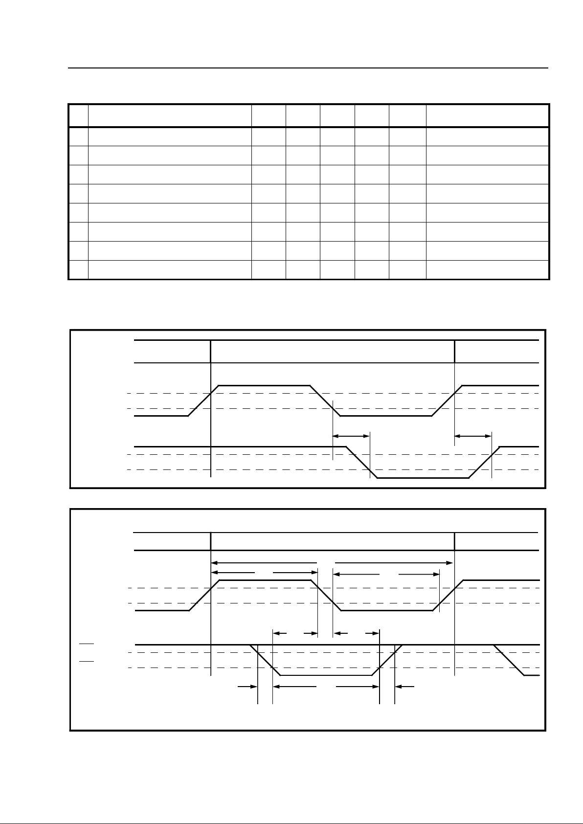
4-211
Preliminary Information MH89790B
Note 1 - The difference between T
TSD
for OUTA and OU TB is ty ic a lly 2 0 ns .
† Timing is over recommended operating temperature and power supply voltage ranges.
‡ Typical figures are at 25°C and are for design aid only: not guaranteed and not subject to prod ucti on testin g.
Figure 25 - Transmit Timing for CEPT Link
FIgure 26 - Receive Timing for CEPT Link
AC Electrical Characteristics† - CEPT Link Timing (Figures 25 and 26)
Characteristics S ym M in Typ‡Max Units Test Conditions
1 T ransmit Steering Delay t
TSD
150 ns See Figure 27, Note 1
2 E2o Clock Period t
PEC
488 ns
3 E2o Clock Width High or Low t
WEC
244 ns
4 Receive Data Setup Time t
RDS
50 ns
5 Receive Data Hold Time t
RDH
50 ns
6 Receive Data Pulse Width t
RDW
244 ns
7 Receive Data Fall Time t
RDF
20 ns
8 Receive Data Rise Time t
RDR
30 ns
Transmitted CEPT Link
Bit Cells
C2i
OUTA
or
OUTB
Bit Cells
V
IH
V
IL
11.8V
1.2V
t
TSD
t
TSD
Received CEPT Link
Bit Cells
E2o
RxA
or
RxB
V
OH
V
OL
V
OH
V
OL
Bit Cell
t
WEC
t
PEC
t
WEC
t
RDS
t
RDH
t
RDF
t
RDW
t
RDR
Page 26
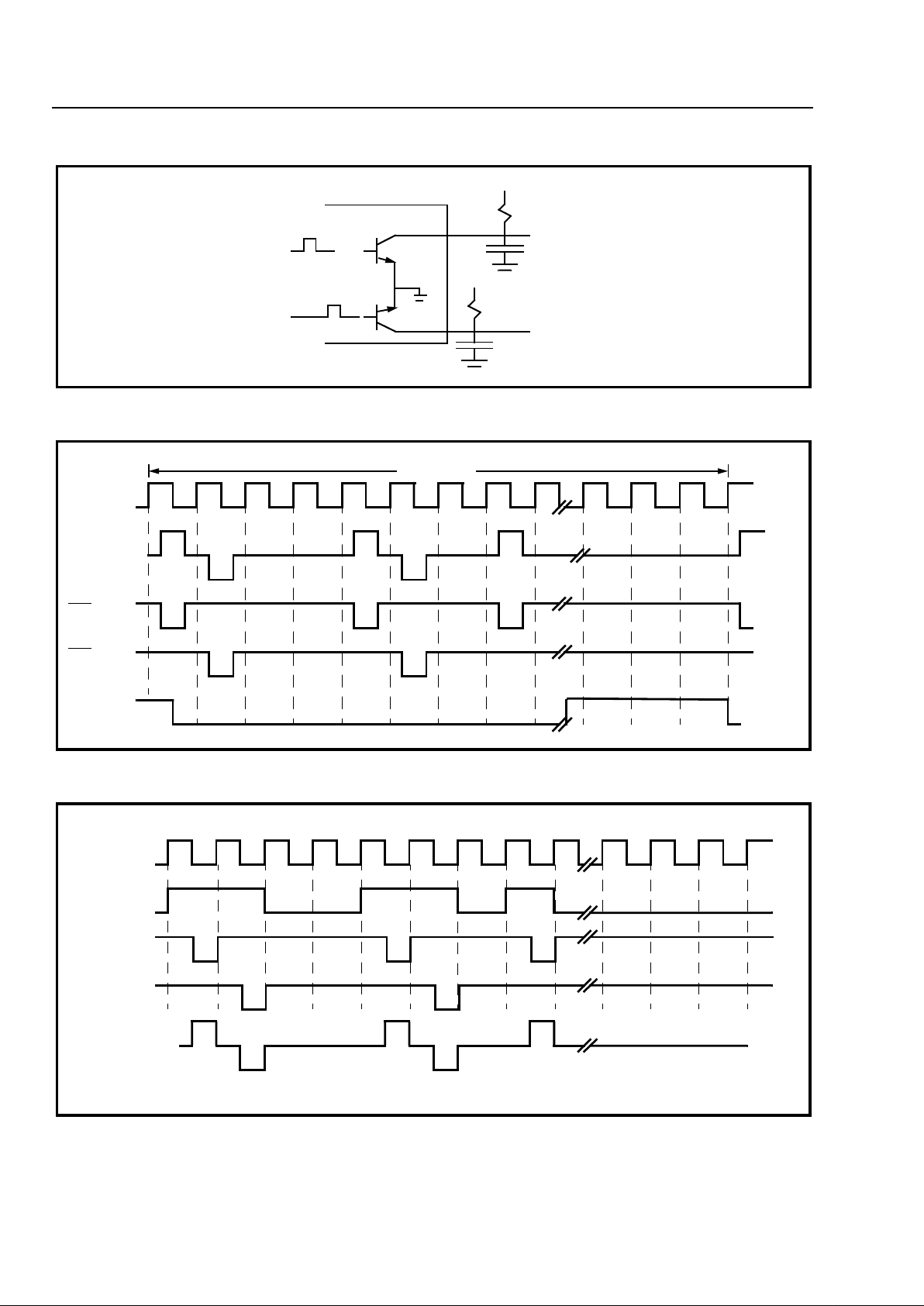
4-212
MH89790B Preliminary Information
Figure 27 - OUTA and OUTB Test Circuit
Figure 28 - CE PT Rec eiv e Tim i ng
Figure 29 - CEP T Transmit Timin g
OUTA
OUTB
•
•
•••
+5V
+5V
•
•
(+ 12V)
400Ω
400Ω
(+ 12V)
50pF
50pF
E2o
HDB3
RxA
RxB
E8K0
125µSec
C2i
INT DATA
OUTA
OUTB
HDB3
Page 27
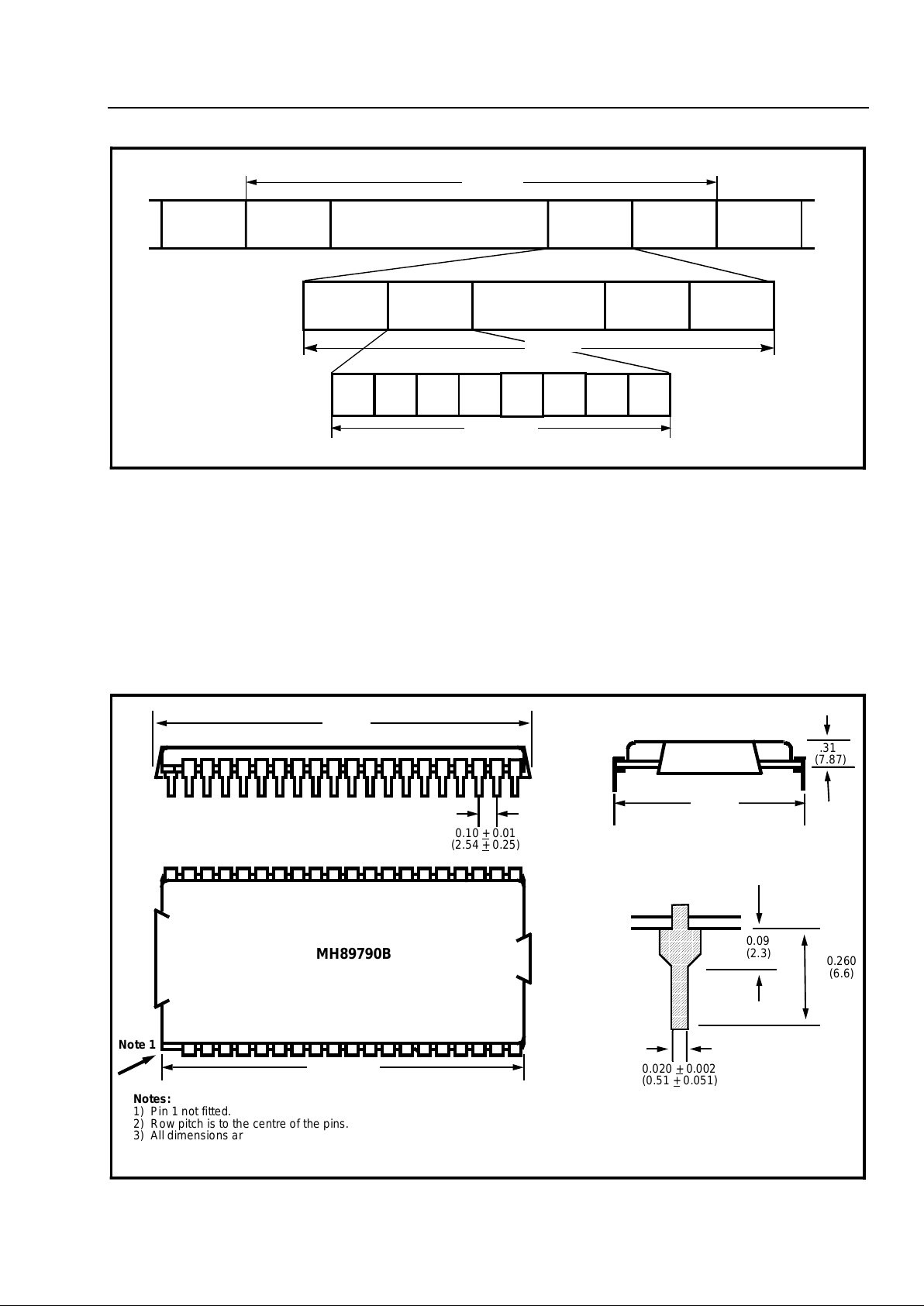
4-213
Preliminary Information MH89790B
Figure 30 - CEPT PCM 30 Frame & Multiframe Formats
FRAME
15 0 14 15 0
TIMESLOT
01 3031
Most
Significant
Bit (First)
Least
Significant
Bit (Last)
Bit
12345678
FRAMEFRAMEFRAMEFRAME
TIMESLOT TIMESLOT TIMESLOT
Bit Bit Bit Bit Bit BitBit
• • • • • • • •
2.0 ms
125µs
(8/2.048)µs
• • • •
Figure 31 - Physical Dimensions for the 40 Pin Dual in Line Hybrid 1.3" Row Pitch
AAAA
AAAA
AAAA
AAAA
AAAA
AAAA
AAAA
AAAA
AAAA
AAAA
AAAA
AAAA
AAAA
AAAA
AAAA
AAAA
AAAA
AAAA
AAAA
AAAA
AAAA
AAAA
.31
(7.87)
0.260
(6.6)
0.09
(2.3)
0.020 +
0.002
(0.51 + 0.051)
0.10 +
0.01
(2.54 + 0.25)
MH89790B
Note 1
Notes:
1) Pin 1 not fitted.
2) Row pitch is to the centre of the pins.
3) All dimensions are typical and in inches (mm).
4) Not to scale.
2.12
(53.85)
1.3
(33.0)
Note 2
2.0
(50.8)
Packaging
The MH89790B is available in three package options
which are:
• The MH89790B which is pin compatible with the
MH89790, has a row p itch o f 1.3” an d is fitted
with a plastic lid. See Figure 31 for the
dimension al draw ing f or this par t.
• The MH8979 0BN whic h is a narr ow ve rsion of
the MH89790B and has a row pitch of 0.8”. See
Figure 32 for t he dimen sio nal dra wing fo r this
part.
• The MH8979 0BS wh ich is a surf ace mo unta ble
version of th e MH8 9790BN is sui table f or
Infrared Reflow (I.R.) soldering. See Figure 33
for the dimen siona l drawi ng, a nd Figure 34 for
the recommended footprint.
Page 28
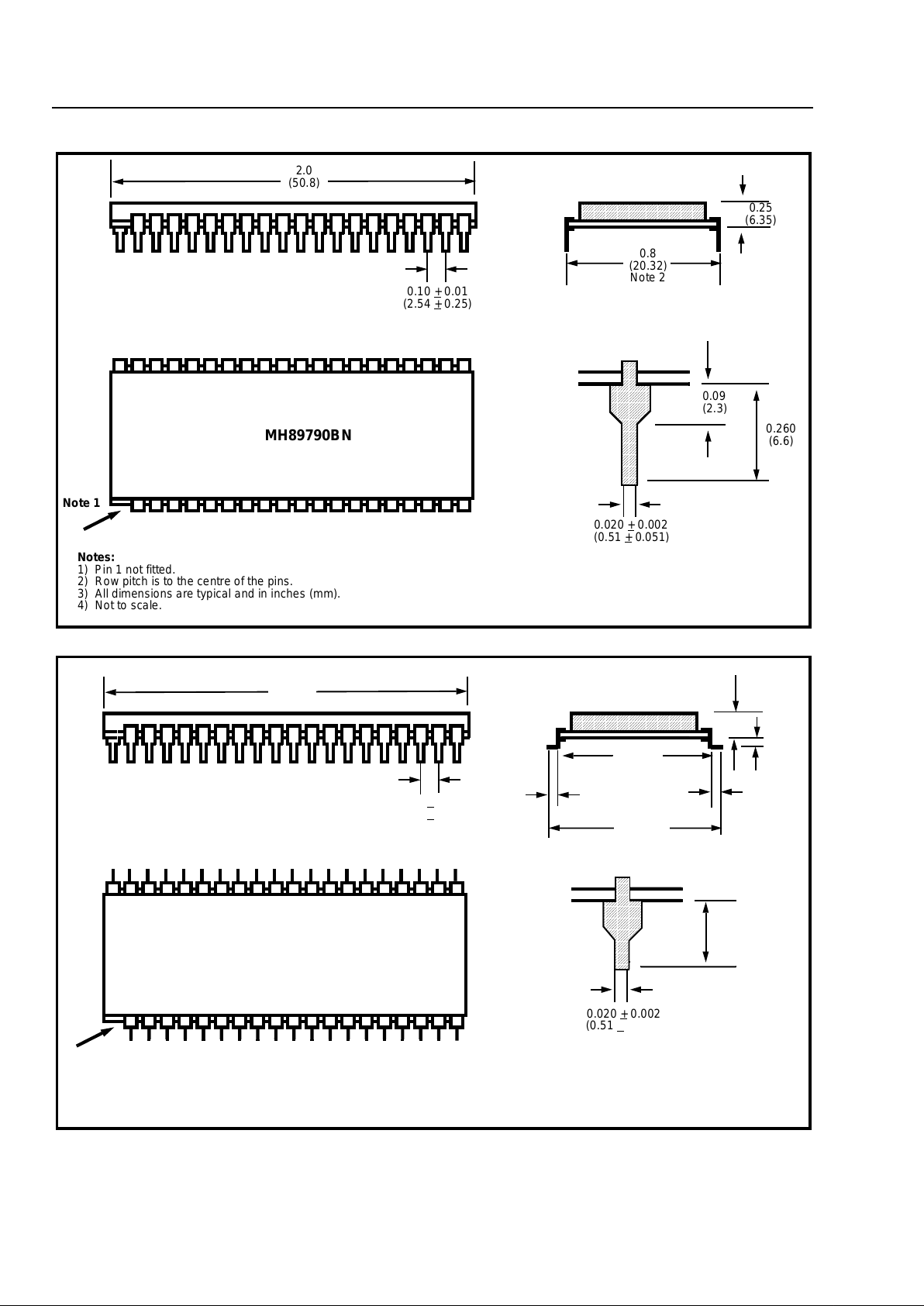
4-214
MH89790B Preliminary Information
Figure 32 - Physical Dimensions for the 40 Pin Dual in Line Hybrid 0.8" Row Pitch
Figure 33 - Ph ysi cal Dim ensio ns for the 40 Pin Dual i n Line S .M.T. Hybrid
AAA
AAA
AAAA
AAAA
AAAA
AAAA
AAAA
AAAA
AAAA
AAAA
AAAA
AAAA
AAAA
AAAA
AA
A
AA
A
AAA
AAAA
AAAA
AAAA
AAAA
AAAA
AAAA
AAAA
AAAA
AAAA
AAAA
AAAA
AAAA
AAAA
AAAA
AAAA
AAAA
AAAA
AAAA
AAAA
AAAA
AAAA
AAAA
MH89790BN
Note 1
Notes:
1) Pin 1 not fitted.
2) Row pitch is to the centre of the pins.
3) All dimensions are typical and in inches (mm).
4) Not to scale.
0.10 +
0.01
(2.54 +
0.25)
0.09
(2.3)
0.260
(6.6)
0.25
(6.35)
0.020 +
0.002
(0.51 +
0.051)
0.8
(20.32)
Note 2
2.0
(50.8)
AAA
AAA
AAAA
AAAA
AAAA
AAAA
AAAA
AAAA
AAAA
AAAA
AAAA
AAAA
AAAA
AAAA
AA
A
AA
A
AAA
0.020 + 0.002
(0.51 + 0.051)
0.10 +
0.01
(2.54 + 0.25)
MH89790BS
Note 1
Notes:
1) Pin 1 not fitted.
2) All dimensions are typical and in inches (mm).
3) Not to scale.
2.0
(50.8)
0.78
(19.81)
0.9
(22.86)
AAAA
AAAA
AAAA
AAAA
AAAA
AAAA
AAAA
AAAA
AAAA
AAAA
AAAA
AAAA
AAAA
AAAA
AAAA
AAAA
0.25
(6.35)
0.125
(3.18)
0.06
(1.52)
0.06
(1.52)
0.125
(3.18)
Page 29
4-215
Preliminary Information MH89790B
Figure 34 - Recommended Footprint for the 40 Pin Dual in Line S.M.T. Hybrid
0.760
(19.3)
Pin 2 position
0.040
(1.02)
0.060
(1.52)
0.090
(2.29)
Page 30

4-216
MH89790B Preliminary Information
Appendix
Control and Status Register Summary
Master Control Word 1 (MCW1) - CSTi0, Channel 15
Master Control Word 2 (MCW2) - CSTi0, Channel 31
Master Control Word 3 (MCW3) - CSTi1, Channel 18
Per Channel Control Word - CSTi0, Channel s 0-14 and 16-30
Channel Associ ated Signa llin g - CSTi1, Chan nel s N = 1 to 15
Frame Alignm e nt Sign al - CSTi1 , Channel 16
Multiframe Al ignm ent Si gna ls - CSTi1, Channel 0
Non-Frame Alignment Signal - CSTi1, Channel 17
76543210
UNUSED
Keep at 1
LOOP16
1 Enabled
0 Disabled
UNUSED
Keep at 1
NDBD
1 No
Debounce
0 Debounce
NDBC
1 No
Debounce
0 Debounce
NDBB
1 No
Debounce
0 Debounce
NDBA
1 No
Debounce
0 Debounce
UNUSED
Keep at 1
UNUSED
Keep at 0
CCS
1 Common
Channel
0 Channel
Associated
8 kHz SEL
1 Enabled
0 Disabled
TXAIS
1 Alarm On
0 Alarm Off
TXTS16AIS
1 Alarm On
0 Alarm Off
XCTL
1 Set High
0 Cleared
UNUSED
UNUSED
Keep at 0
SiMUX
1 Enabled
0 Disabled
RMLOOP
1 Enabled
0 Disabled
HDB3en
1 Disabled
0 Enabled
Maint
1 Enabled
0 Disabled
CRCen
1 Enabled
0 Disabled
DGLOOP
1 Enabled
0 Disabled
ReFR
Device
reframes on
High to Low
Transition
DATA
1 No ADI
0 Enable ADI
LOOP
1 Enabled
0 Disabled
RxPAD4 RxPAD2 RxPAD1 TxPAD4 TxPAD2 TxPAD1
A(N)
Tx
Signalling Bit
B(N)
Tx
Signalling B it
C(N)
Tx
Signalling Bit
D(N)
Tx
Signalling B it
A(N+15)
Tx
Signalling Bit
B(N+15)
Tx
Signalling B it
C(N+15)
Tx
Signalling Bit
D(N+15)
Tx
Signalling Bit
IUO
Should be
kept at 1
FAF2-8
Frame Alignment Signal - Keep at "0011011"
MA1-4
Multiframe Alignment Signal - Keep at "0000"
X1
Spare Bit
Should be 1
Y
1 Alarm On
0 Alarm off
X2, X3
Spare Bits - Should be 1
IU1
Reserved for
International
Used
NFAF
Keep at "1"
ALM
1 Alarm On
0 Alarm Off
NU1-5
Bits Reserved for National Use - Should be kept at "1"
Page 31

4-217
Preliminary Information MH89790B
Master Status Word 1 (MSW1) - CSTo, Channel 18
Master Status Word 2 (MSW2) - CSTo, Channel 21
Phase Status Word - CSTo, Channel 19
CRC Error Counter - CSTo, Channel 20
Received Channel Associated Sign alling - CSTo, Channels N = 1 to 15
Received Fr am e Align m ent Sign al - CSTo, Channel 16
Received Multifram e Alignme nt Sign als - CSTo, Channel 0
Received Non -Fram e Alig nmen t Signal - CS To, Channel 17
76543210
TFSYN
1 Out of Sync
0 In Sync
MFSYN
1 Out of Sync
0 In Sync
ERR
Frame
Alignment
Signal Error
Count
SLIP
Changes
State when
Slip
Performed
RXAIS
1 Alarm
Detected
0 No Alarm
TXTS16AIS
1 Alarm
Detected
0 No Alarm
XS
1 XSt High
0 XSt Low
UNUSED
Si2
Remote SM F2
is:
1 Correct
0 Errored
Si1
Remote SMF1
is:
1 Correct
0 Erro re d
UNUSED CRC Timer
Transition
from 1 to 0
indi ca tes start
of the CRC
Error Count
CRC Ref
1 Reframed
forced by lack
of CRC frame
CRC Sync
1 CRC Frame
not Detected
0 CRC Frame
Detected
FrmPhase
Bit 8 of Phase
Status Word
TxTSC
Transmit Timeslot Count, Timeslots between F0i and E8Ko
TxBTC
Transmit Bit Count - bit positions within TxTSC
between F0i and E8Ko
CERC 0 - 7
Bits 0 - 7 of CRC Error Counter
A(N)
Rx
Signalling Bit
B(N)
Rx
Signalling B it
C(N)
Rx
Signalling Bit
D(N)
Rx
Signalling B it
A(N+15)
Rx
Signalling Bit
B(N+15)
Rx
Signalling B it
C(N+15)
Rx
Signalling Bit
D(N+15)
Rx
Signalling Bit
IUO
International
Bit
FAF2-8
Received Frame Alignment Signal
MA1-4
Received Multiframe Alignment Signal
X1
International
Bit
Y
1 Remote MF
Lost
0 Remote MF
Detected
X2, X3
International Bits
IU1
Reserved for
International
Use
NFAF ALM
1 Detected
0 Not
Detected
NU1-5
Bits Reserved for National Use
Page 32

4-218
MH89790B Preliminary Information
NOTES:
 Loading...