

Page 1
CMOS ST-BUS FAMILY
MT8910-1
Digital Subscriber Line Interface Circuit
Preliminary Information
Features
• Compatible with ISDN U-Interface standard
• Over 40 dB (
@40 k Hz) of loop a tte nuation
• Full dup lex tr ansmi ssi on ov er singl e twis ted
pair
• Adva nced ec ho can cel ling techno logy
• High p erforma nce 2B1Q li ne code
• Full act ivat ion/de activ atio n state m ac hine
• QSNR an d line attenu ati on diag no stics
• Frame and superframe synchronization
• On-chip 15 second timer
• Inser tion loss me asur emen t test signal & quiet
mode
• Mitel ST-BUS compat ible
• Single 5V powe r supp ly
Applications
• ISDN NT1 a nd NT2 DSL interfa ce
• Digita l PABX line cards an d tel ephon e sets
• Digita l multip lexers an d con cen trators
• Pair gain system
ISSUE 1 August 1993
Ordering Information
MT8910-1AC 28 Pin Ceramic DIP
MT8910-1AP 44 Pin PLCC
0°C to +70 °C
Description
The MT8910-1 Digital Subscriber Line Interface
Circuit (DSLIC)
rate access (2B+D) at the U-interface. Full duplex
digital trans mission at 160 kbit/s on a single twiste d
pair is achieved using echo cancelling hybrid (ECH)
technology. This, in conjunction with the high
performance 2B1Q line code, allows the DSLIC to
meet the loop length requirements of the digital
subscriber loops at the U-interface over the entire
non-loaded telephone loop plant.
The MT8910-1 is compatible with the complete
range of Mitel Semiconductor ISDN components
through the use of the ST-BUS interface.
is designed to provide ISDN basic
DSTi
CDSTi
MRST
F0b
C4b
SFb
F0od
MS0
MS1
NT/LT
CDSTo
DSTo
Transmit
Interface
Control
Register
TRANSMIT/
RECEIVE TIMING
& CONTROL
INTERFACE
Status
Register
Receive
Interface
VSS AVSS VDD AVDD OSC2 OSC1
Scrambler
& Encoder
Framing
&
Mainte nance
Descrambler,
Decoder &
Diagnostics
Jitter
Compen-
sator
Decision
Feedback
Equalizer
Quantizer
Figure 1 - Functional Block Diagram
Linear
Echo
Canceller
TSTin TSTout
DAC and
Tx Filter
Non-
Linear
Compen-
sator
Timing
Adaptation
Circuit
TSTen
+
-
Tone
Detector
2nd Order
PDM ADC
FIR
Digital Filter
Bias &
Voltage Ref.
VRef VBias
Lout+
Lout-
Lin+
Lin-
9-3
Page 2
MT8910-1 Preliminary Information
TSTin
AVSS
Lout+NCNC
Lin+
Lin-
VRef
VBias
Lout-
NC
Lout-
Lout+
AVSS
TSTin
CDSTi
DSTi
VSS
DSTo
CDSTo
F0od
TSTout
MS0
MS1
NT/LT
1
2
3
4
5
6
7
8
9
10
11
12
13
14
28 PIN CERDIP
28
27
26
25
24
23
22
21
20
19
18
17
16
15
Lin+
LinVRef
VBias
AVDD
IC
VDD
MRST
OSC1
OSC2
F0b
C4b
SFb
TSTen
NC
CDSTi
NC
NC
NC
DSTi
VSS
DSTo
CDSTo
F0od
NC
65432 44434241
7
8
9
10
11
12
13
14
15
16
17
MS0
TSTout
1
231819202122 2425262728
MS1
SFb
NT/LT
TSTen
44 PIN PLCC
NC
NC
C4b
29
39
38
37
36
35
34
33
32
31
30
F0b
40
NC
NC
AVDD
NC
NC
NC
IC
VDD
MRST
OSC1
OSC2
NC
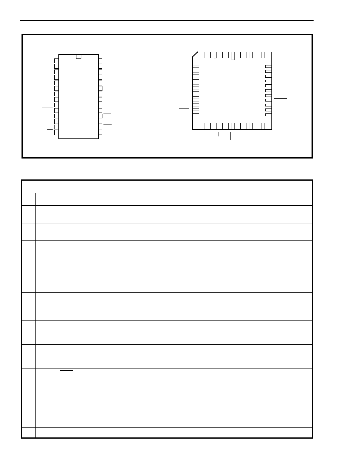
Figure 2 - Pin Connections
Pin Description
Pin #
Name Description
DIP PLCC
11 L
23 L
35AV
46TSTinI/O Structure Test Input. When TSTen is high, TSTin is used as a source to all output
Line Out Minus. One of a pair of differential analog out put s for the 80 kbaud/ s 2B1Q
out-
signal, biased at V
Line Out Plus. One of a pair of differential analog outputs for the 80 kbaud/s 2B1Q signal,
out+
biased at V
Analog Ground. Tie to VSS.
SS
Bias
.
Bias
.
drivers. Refer to “I/O Structure Test" in functional descript ion fo r more details. Tie to V
for normal operation.
SS
5 8 CDSTi Control/Data ST-BUS Input. A 2048 kbit/s serial PCM/data input for the D- and
C-channels in Dual mode. Unused in Single mode and should be connected to V
SS
.
612DSTiData ST-BUS Input. A 2048 kbit /s serial PCM/ dat a input for the D-, C-, B1- and B2-
channels in Single mode. In Dual mode, only the B- channels are input .
713 V
SS
Ground .
814DSToData ST-B US Outpu t. A 2048 kbit/s serial PCM/dat a output for th e D-, C-, B1- and B2-
channels in Single mode. In Dual mode, only the B- channels are outp ut. This output is
placed in high impedance during the unused channel times.
9 15 CDSTo Control/Data ST-BUS Output. A 2048 kbit/s serial PCM/data output for t he D- and
C- channels in Dual mode. It is placed in high impedance in Single mode, and during the
unused channel ti mes in Dual mo de.
10 16 F0od
Delayed Frame Pulse Ou tp ut. A 244 ns wide negative going pulse indicat ing the end of
the active ST-BUS channel times of the device to allow for daisy-chaining of other ST-BUS
devices. Active after channel 0 in Dual Port mode and Channel 3 in Single Port Mode.
11 18 TSTout I /O Structure Test Output. When TSTen is high, the TSTout provides the output of an
XOR chain which is sourced from all digital inputs. Refer to “I/O Structure Test " in
functional description for more deta ils. Leave unconnected for normal operation.
12 19 MS0 Mode Select 0. CMOS input. Refe r to Table 1.
13 20 MS1 Mode Select 1. CMOS input. Refe r to Table 1.
9-4
Page 3
Preliminary Information MT8910-1
Pin Description (continued)
Pin #
Name Description
DIP PLCC
14 21 NT/LT NT/LT Mode Select. CMOS Input. When high, the DSLIC is setup in NT mode. When
low, LT mode is selected.
15 22 TSTen I/O Structure Test Enable Input. This active high input ena bles the bui lt-in test of all
digital input and output structures. Refer to “I/O Structure T est" in functional description for
16 23 SFb
more details. Tie to V
Superframe Pulse. In LT mode, an input pulse once every superframe (12 ms) which,
when low during a falling edge of C4 b
superframe boundary.
In NT mode, a 244 ns wide output pulse once every 12 ms indicating the boundary of the
transmit superframe. In NT mode, the superframe timing is generated from the line signal
time base and, as such, SFb will only be valid once the transceiver has achieved full
activation.
for normal operation.
SS
within an F0b low pulse, sets the transmit
17 25 C4b
4096 kHz Data Clock. In LT mode, a 4096 kHz ST-BUS clock input. In NT mode, a 4096
kHz ST-BUS clock output frequency locked to the line signal.
18 27 F0b
Frame Pul se. In LT mode, an 8 kHz input pulse indicating the start of the active ST-BUS
channel times. In NT mode, an 8 kHz output pulse extracted from the line signal indicating
the start of the active ST-BUS channel times.
19 30 OSC2 Oscillator Ou tpu t. When the MT8910-1 operate s with an External Clock (typicall y LT
mode) connect OSC2 to the output of an external inverter providing a 10.24 MHz ±5ppm
clock (see “10.24 MHz Clock Interface" section).
When operating wit h a crystal (typically NT mode) connect one lead of the fundam ental
mode parallel resonator crystal (10.24 MH z ±50ppm in case of NT mode).
20 31 OSC1 Oscillator In pu t. When the DSLIC operat es with an External Clock (typical ly LT mode)
connect OSC1 to the input of an external inverter (see Fig.11).
When operating wit h a crystal (typically NT mode) connect the other lead of the
fundamental mode parall el resonato r crystal (10.24 MHz ±50ppm in case of NT mode).
21 32 MRST
22 33 V
Master Reset. Active low CMOS input performs a master reset of the DSLIC .
Power Supp ly Inpu t.
DD
23 34 IC Internal Connection. Leave unconn ected.
24 38 AV
25 41 V
26 42 V
27 43 L
28 44 L
2,4,7,
9 -11,
17,24
26,28
29,35
36,37
39,40
NC No Connection. Leave circuit open.
Analog P ow er Su pp ly. Connect to VDD.
DD
Bias Voltage. Decouple to AVSS through a 1.0 µF ceramic capacitor.
Bias
Reference Voltage. Decouple to AVSS through a 1.0 µF ceramic capacitor.
Ref
Line Signal Input Minus. Internally biased at V
in-
Line Signal Input Plus. Internally biased at V
in+
Bias.
Bias.
9-5
Page 4

MT8910-1 Preliminary Information
Functional Description
The MT8910-1 Digital Subscriber Line Interface
Circuit (DSLIC) is a high performance, full duplex
transceiver which provides a complete interface to
the U-reference point as specified in ANSI T1.601-
1988. Operating in either master Line Terminator
(LT) mode or slave Network Terminator (NT) mode,
the DSLIC can be configured to operate at either end
of the Digital Subscriber Line (DSL). The DSLIC
supports full duplex transmission of a 2B + Dchannel format at 160 kbit/s over a single twisted
pair with about 40 dB of loop attenuation at 40 kHz.
To achieve this transmission performance, the
DSLIC uses a 2B1Q line code which is a four level
pulse amplitude modulated (PAM) signal with no
redundancy. This line code was approved by the
American National Standards Institute technical
committee T1E1. Using this line code, two binary
bits are converted into one four level quaternary
symbol. This results in an effective baud rate
reduction from 160 to 80 kbaud/s allowing the
transmission to benefit from reduced line attenuation
and improved immunity to near end crosstalk
(NEXT).
To complement the performance of the 2B1Q line
code, the DSLIC uses an advanced echo cancelling
hybrid (ECH) technique, by means of a transversal
filter, that provides greater than 60 dB of echo
cancellation. This cancellation, along with all
equalization, is performed in the digital domain using
dedicated DSP hardware. Since a digital transversal
echo canceller gives a linear representation of the
echo, the MT8910-1 also has a non-linear echo
canceller which works in parallel with the transversal
filter to compensate for non-linearities in the transmit
path and the passive line termination. In addition, a
jitter compensator is used to correct errors in the
echo estimates which are sourced from corrections
in the received timebase. The jitter compensator will
interact directly with the echo taps in the transversal
filter.
A block diagram of the DSLIC is shown in Figure 1.
The DSLIC has two ports consisting of a serial
system interface (Mitel's standard ST-BUS), and a
line port which interfaces directly to the single
twisted pair via a passive termination hybrid and a
line pulse transformer.
The two B-channels and the D-channel to be
transmitted on the line are input to the DSLIC (on the
ST-BUS) into the transmit interface block. The sync
word and maintenance bits are added to the data
which is then formatted, scrambled and digitally
encoded into 2B1Q symbols. This digital
representation is passed through a finite impulse
response filter which converts the digital
representation into an analog waveform. The
transmitted pulse is then passed through a
smoothing filter whose output is passed to a
differential line driver which is driving t he line through
a passive hybrid network and line pulse transformer.
On the receive side, the pre-cancelled signal drives
a balanced receiver which feeds the input to an oversampled second-order delta sigma A/D converter.
The digital representation of the received signal
yields a Pulse Density Modulated (PDM) stream
which is digitally filtered and decimated to the 80 kHz
baseband. Intersymbol interference (ISI) introduced
by the loop is cancelled by a decision feedback
equalizer. This is achieved by taking a convolution
of the received pulse with the estimated impulse
response of the loop. The cancellation of ISI is
performed in parallel with the echo cancellation.
Estimated received echo is obtained by taking the
convolution of the transmit signal with the estimated
impulse response of the loop. Feedback from the
jitter compensator and the non-linear corrector
interact with the coefficients of the echo canceller to
reduce the error introduced by jitter and nonlinearities in the analog circuitry. The output of all
these blocks is summed together and the result is
the received data which is passed through a decoder
and descrambler before being sent out in TDM
bursts on the ST-BUS.
Line Port
The DSLIC interfaces to the U-reference point as
defined in the ISDN Basic Access Reference model.
As such, the transceiver transfers full duplex, time
division multiplexed data at 160 kbit/s. This includes
two 64 kbit/s PCM voice or data channels (Bchannels), a 16 kbit/s signalling channel (D-channel)
and 16 kbit/s for synchronization and overhead.
The two 64 kbit/s channels are defined as the B1and B2-channels and they carry subscriber
information such as digitally encoded voice, circuit
switched data or packet switched data. The DSLIC
will transfer both B-channels transparently from the
ST-BUS port to the line port and vice versa once the
device has acquired superframe synchronization.
The 16 kbit/s D-channel is primarily intended to carry
signalling information for circuit switching the Bchannels through the ISDN network. The D-channel
can optionally carry packetized information and
telemetry services. The D-channel is transmitted
transparently through the DSLIC from the ST-BUS
port to the line port and vice versa once the device
has acquired superframe synchronization. It is to be
9-6
Page 5
Preliminary Information MT8910-1
noted that the system interface has dedicated a full
64 kbit/s for the D-channel of which only the two first
bits (D0 and D1) are actually carrying information.
The other bits of the ST-BUS D-channel are reserved
for future use.
A third type of channel, the C-channel, is a nonbearer channel which provides a means for the
system to control and monitor the functionality of the
DSLIC. This control/status channel is accessed by
the system through the ST-BUS. The C-channel
provides access to three control registers and four
status registers which provide complete control or
status of all built-in features. Access to the control
register is provided by two bits in the Control
Register itself (CRS0 and CRS1). Selection of the
desired status register is performed using two bits in
Control Register 1 (SRS0 and SRS1). The Cchannel also carries a control and status register for
the 4 kbit/s M-channel which can be used as an
additional maintenance channel. A detailed
description of these registers is discussed in the STBUS port interface section.
Line Code
The DSLIC transceiver uses the 2B1Q line code
which is a four level Pulse Amplitude Modulated
(PAM) code with no redundancy. The generation of
the 2B1Q signal is achieved by grouping two
consecutive bits into a bit field of which the first bit
represents the sign bit and the second represents
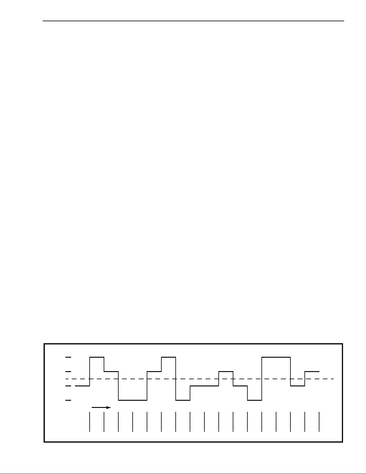
the magnitude. This yields four possible output
codes as shown in Figure 3 (note that +3, +1, -1 and
-3 are only symbols and they do not reflect the
voltage on the line).
The bit fields are grouped relative to the borders of
the defined channels where the first bit field consists
of bit 1 and bit 2 of the B1-channel, the second bit
field consists of bit 3 and bit 4 of the B1-channel
and so on.
Before con verting the bit fields into outp ut symbols,
all bits except the framing pattern are scrambled with
polynom i als:
(where
-5
⊕ x
1
1
-18
⊕ x
⊕ is modulo two summation)
⊕ x
⊕ x
-23
for LT
-23
for NT
Framing
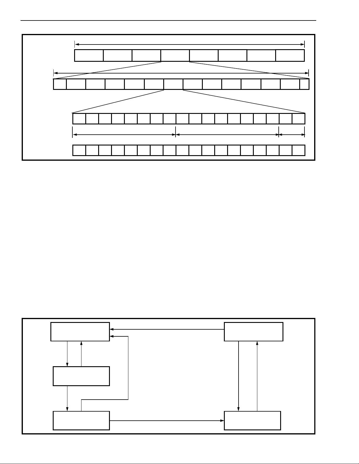
The frame structure in the DSLIC is 1.5 ms long and
consists of twelve 2B+D-channels delimited by the
framing pattern at the start of the frame and the
maintenance channel at the end. Framing for both
the LT and the NT is performed using a 9 symbol
synchronization word. This sync word (SW) has the
following structure:
Sync Word: + 3, + 3 , -3 , -3 , - 3 , + 3 , - 3, + 3 , + 3
Eight DSLIC frames are grouped into a superframe
delimited by inverting the sync word (ISW):-3,-3, +3,
+3, +3, - 3 , + 3 , -3 , -3 . This s ec o nd l ev e l o f framing i s
used to assign the M-channel bits as defined in the
ANSI T1.601-1988. The framing structure is shown
in Figure 4.
Transmission between the LT and NT is fully
synchronous. As such, the frame/superframe
boundaries between the NT receive frame and the
NT transmit frame have a fixed phase relationship.
The transmitted frame/superframe from the NT is
delayed by 60 ± 2 quaternary symbols (quats) with
respect to its received frame/superframe. Since the
NT extracts all i ts timing from t he li n e , the D SL IC will
maintain the required phase relationship between
the frames and superframes and will insert the SW
and ISW during the proper time interval.
+3
+1
-1
-3
time
QUATS -1 +3 +1 -3 -3 +1 +3 -3 -1 -1 +1 -1 -3 +3 +3 -1 +1
BITS 0 1 1 0 1 1 0 0 0 0 1 1 1 0 0 0 0 1 0 1 1 1 0 1 0 0 1 0 1 0 0 1 1 1
Figure 3 - Example of 2B1Q Quaternary Symbols
9-7
Page 6
MT8910-1 Preliminary Information
12 ms
Superframe
Frame
Information
Channels
Corresponding
ST-BUS
SW 2B + D 2B + D 2B + D 2B + D 2B + D 2B + D 2B + D 2B + D 2B + D 2B + D 2B + D 2B + D M
Frame 1 Frame 2 Frame 3 Frame 4 Frame 5 Frame 6 Frame 7 Frame 8
B11 B12 B13 B14 B15 B16 B17 B18 B21 B22 B23 B24 B25 B26 B27 B28 D1 D2
50 µs
B7 B6 B5 B4 B3 B2 B1 B0 B7 B6 B5 B4 B3 B2 B1 B0 D0 D1
Figure 4 - F rame S truc ture
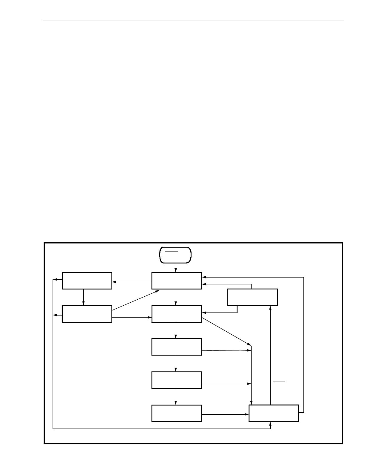
Basic Frame Synchronization (BFS) is achieved
using the algorithm shown in Figure 5. The DSLIC
searches for the sync word or the inverted sync word
within the received data stream. After detecting
three consecutive synchronization patterns spaced
exactly 120 quats apart, the DSLIC declares terminal
synchronization by setting the bits of the Internal
State Indicator to 111 in Status Register 1. A loss of
synchronization is declared by the DSLIC when at
least one of the nine quats at the beginning of each
Basic Frame differs by more than one quantization
level for two consecutive frames.
A search for superframe synchronization will begin
only after Basic Frame sync has been found. The
DSLIC will declare superframe sync (SFS) on the
first occurrence of the properly spaced Inverted Sync
Word (ISW) once Basic Frame sync has been
acquired. The synchronized state is identified by the
1.5 ms
50 µs
12.5 µs
status of internal state bits IS2, IS1 and IS0 found in
Status Register 1.
The DSLIC will lose superframe sync under three
conditions;
1) if the DSLIC loses basic frame sync,
2) if the ISW does not occur exactly eight basic
frames apart,
3) if the ISW is received w hen it is not expect ed.
Activation/ De activ atio n
The DSLIC has a complete activation/deactivation
state machine which allows the user to activate or
deactivate the link as per the requirements in the
9-8
STATE : LOST
BFS : 0
One
Valid
SW
STATE : SENSING1
BFS : 0
One
Valid
SW
STATE : SENSING2
BFS : 0
Error in
SW
> One-Level Error in SW
Error in
SW
One Valid SW
STATE : LOSING
BFS : 1
Valid
SW
STATE : SYNC
BFS : 1
Figure 5 - Frame Synchronization State Diagram
> One-Level
Error in SW
Page 7
Preliminary Information MT8910-1
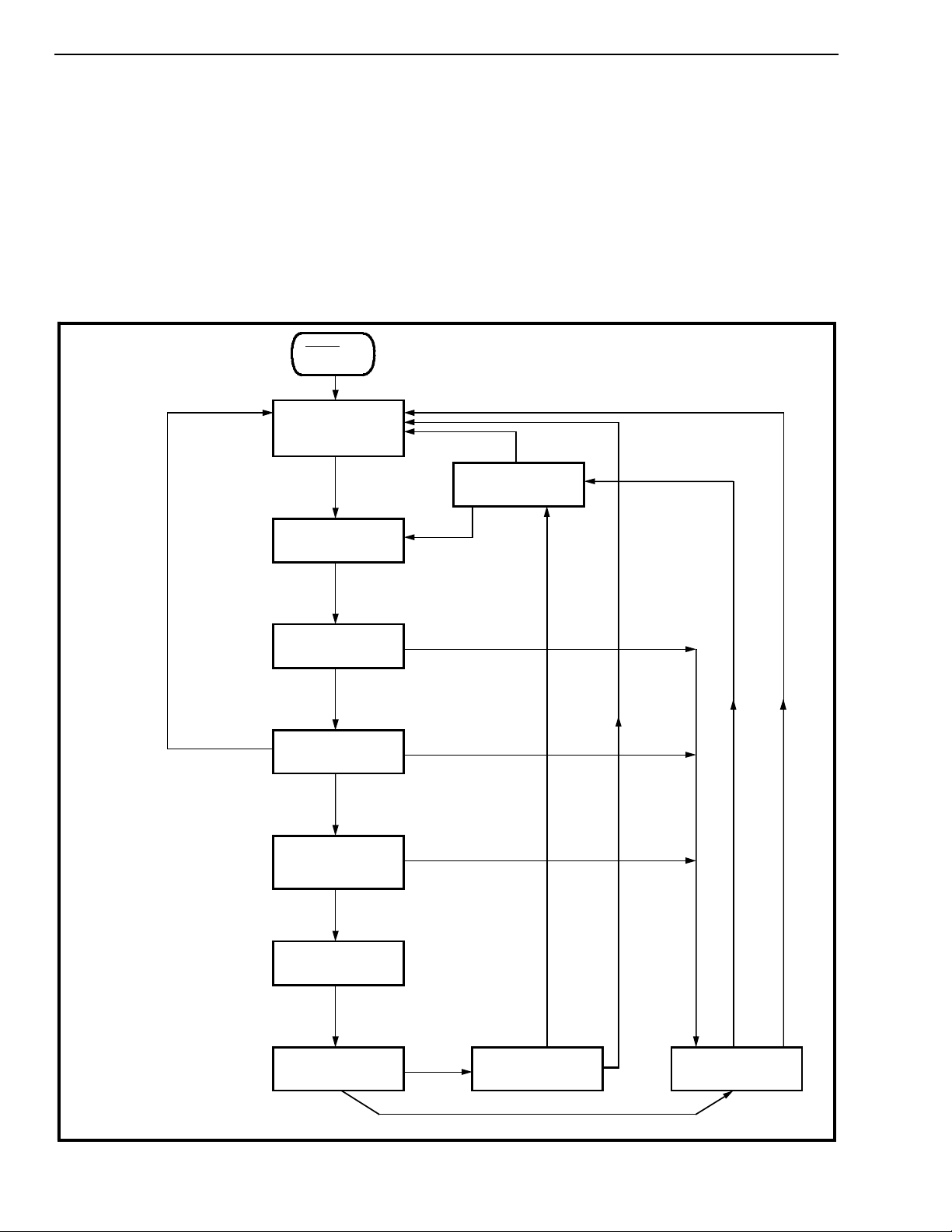
T1.601-1988 standards. The activation sequence for
the DSLIC is mode dependent and is outlined in
Figures 6a) and b).
In the LT mode, the request for activation can be
initiated in two w ay s. Se tting the st art/s top bit in the
Control Register 1 will result in the generation of a
repeated pattern of four +3 symbols followed by four
-3 symbols producing a 10 kHz activation tone (TL)
for 3 milliseconds. The DSLIC can also be activated
by receiving a 10 kHz activation tone from the NT
(TN). Once the NT has generated a tone,
progression through the state machine follows the
algorithm as shown in Figure 6a.
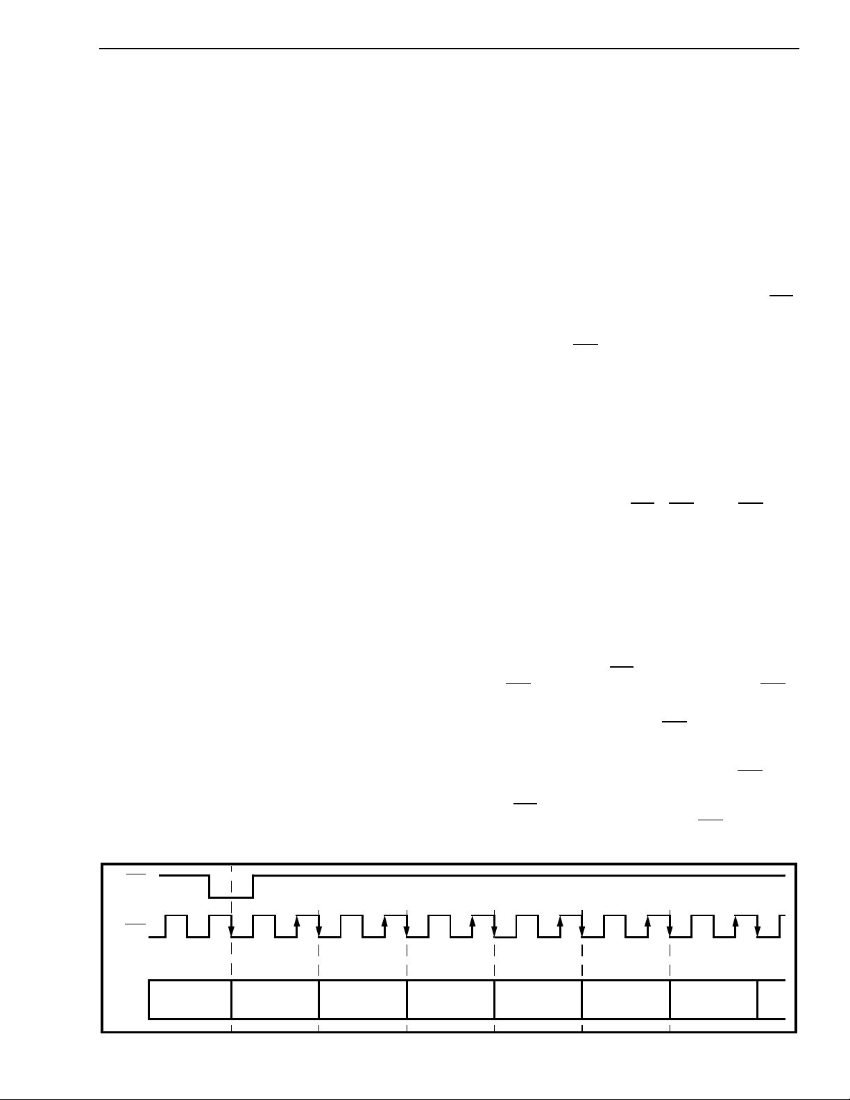
In the NT mode, the request for activation can be
initiated in two w ay s. Se tting the st art/s top bit in the
Control Register 1 will result in the generation of a
repeated pattern of four +3 symbols followed by four
-3 symbols resulting in the transmission of the NT
activation tone (TN). The DSLIC can also be
activated by receiving TL from the LT to which the
NT will respond with its own activation tone (TN).
Progression through the state machine will follow the
algorithm as shown in Figure 6b.
During the activation sequence, there is an extensive
exchange of signals between the LT and the NT.
This handshaking of information is required to allow
individual transceivers to train both their echo
cancellers and decision feedback equalizers. All
possible signals are described below.
• TN: A 10 kHz activatio n t one sourced by the
NT which is ge nerat ed by sen ding a
continuo us pa ttern o f fou r +3 s ymbol s
followed by four -3 symbols.
• SN0: SN0 is a no signal condition which is
used to indica te to the LT that the N T
has finish ed trai ning its ech o can celle r.
• SN1: An NT generated signal consisting of a
framed (b ut not su per framed ),
scrambled 2B1Q signal which carries all
1s in the B-, D- and M-channels. This
signal is used t o train t he NT’s ec ho
canceller.
• SN2: An NT generated signal consisting of a
framed (b ut not su per framed ),
scrambled 2B1Q signal which carries all
1s in the B-, D- and M-channels. This
signal is used t o train t he LT’s DFE.
• SN3: An NT generated signal consisting of a
fully framed and superframed scrambled
2B1Q si gn al w hi ch c ar ri es i nf orm a tio n in
all the B-, D- and M-channels.
Alerting
Tx-TL (3ms)
Awaiting Reply
Tx-SL0
Expiry of T0
ST.T3
T0 = 15 sec timer
T1 = 480 ms timer
ST.T1
ST.Tx = Start Timer x
STP.Tx = Stop Timer x
LAR = Local Activation Request
LDR = Local Deactivation Request
SFS = Superframe Synchronization Acquired
RCV Reset
Tx-SL0
of T0
(Loss of
signal and
LDR),
ST.T3
1
1
: Loss of received signal will result in loss of sync.
Note
ST.T2
STP.T3
Pending Deact.
Tx-SL0
LAR
ST.T0
Expiry of
T1
RCV TN
STP.T1
T2 = 40 ms timer
T3 = 520 ms timer
Pin
MRST
Full Reset
Tx-SL0
RCV TN
ST. T0
Awak e
Tx-SL0
End SN1
EC Training
Tx-SL1
EC
Converged
Framing
Tx-SL2
SFS
STP.T0
Active
Tx-SL3
Expiry of T2
RCV TN
ST.T0
STP.T2
Expiry
Expiry of T0
Expiry of T0
BFS Lost > 480ms
or LDR
ST.T3
Figure 6a - Acti vatio n/Deac tiva tion State Diagra m - LT Mode
(Loss of signal
and LDR) or
Expiry of T3
9-9
Page 8
MT8910-1 Preliminary Information
• TL: A 10 kH z act i v ation tone sourced by the
LT which i s genera ted b y send in g a
continuo us pa ttern o f four +3 sy mbo ls
followed by four -3 symbols.
• SL0: SL0 is a no si gn al cond ition ge ne rated
from the LT.
• SL1: An LT generated signal consisting of a
framed (b ut no t supe rframed ),
scrambled 2B1Q signal which carries all
1s in the B-, D- and M-channels. This
signal is used t o train t he LT’s echo
canceller.
MRST Pin
Full Reset
(Power down
Tx-SNO
RCV TL or
LAR
ST.T0
Alerting
Tx-TN (9 ms)
• SL2: An LT generated signa l co nsis ting of a
fully framed and sup erfram ed
scrambled 2B1Q signal which carries all
0s in the B- a nd D- channe ls w ith
information i n the M-chan ne l. This
signal is used to train the NT’s DFE.
• SL3: An LT generated signa l co nsis ting of a
fully framed and superframed scrambled
2B1Q signal which carries information in
all the B-, D - and M- chan nels.
ST.Tx = Start Timer x
STP.Tx = Stop Timer x
LAR = Local Activation Request
LDR = Local Deactivation Request
SFS = Superframe Synchronization Acquired
Expiry of T2
RCV Reset
Tx-SN0
RCV TL
ST.T0
STP.T2
Loss of signal
STP.T3
ST.T2
Expiry of T1
T0 = 15 sec timer
T1 = 480 ms timer
T2 = 40 ms timer
T3 = 520 ms timer
1
Note
: Loss of received signal will
result in a loss of sync.
EC Training
Tx-SN1
EC
Converged
ST.T1
Quiet
Tx-SN0
Signal
Detected
STP.T1
Train
DFE/Timing
Tx-SN0
SL2
Detected
Framing
Tx-SN2
SFS
Active
Tx-SN3
Expiry of T0
Expiry of T0
Expiry of T0
LDR
ST.T3
Loss of
far-end
signal
STP.T3
ST.T2
Pending Dea ct.
Tx-SN3
Loss of BFS > 480ms
ST.T3
ST.T3
1
Figure 6b - Acti vatio n/Deac tiva tion State Diagra m - NT Mod e
Expiry
of T3
ST.T3
Tear Down
Tx-SN0
9-10
Page 9
Preliminary Information MT8910-1
The reset state consists of two substates, the
receive reset state and full reset state. The full reset
state is entered following a power-up or after the
expiry of the receive reset timer (40 ms). The
receive reset state is a transient state which is
entered once the DSLIC has detected a loss of
received signal while the transceiver is not
transmitting. In this state, the transceiver will not
initiate the start-up sequence but is capable of
responding to the appropriate activation tone. When
the timer in the receive reset state has timed out (40
ms), the t ran sce iver enters the fu l l re se t s ta te .
All timers surrounding the reset states are included
in the DSLIC and have been set as per the ANSIT1.601-1988:
• Failure to complete a start-up sequence
timer is set at 15 seconds.
• Loss of re ceived signal timer i s set at
480 ms as is the loss of
synchronization.
• The receive reset state timer is set to
40 ms.
• A fourth timer (not specified in ANSI
T1.601- 198 8) has be en inc lud ed whic h
will restrict the time to 520 ms for a
deactiv ati on sequence.
The DSLIC will enter a deactivated state on the
assertion of a deactivation request (setting the Start/
Stop bit to 0 in Control Register 1, and the
subsequent loss of the received signal). Once the
deactivation process has been completed, the
request for activation can follow a warm start
process as defined in ANSI T1.601-1988.
The MT8910-1 is production tested for error free
performance for 2.5 sec (20,000 ST-BUS) frames
over a 4.6km (15 kft) 26 AWG simulated loop
(equivalent to 40dB attenuation @ 40 kHz).
ST-BUS Interface
The ST-BUS is a synchronous time division
multiplexed serial bussing scheme with data streams
operating at 2048 kbit/s configured as 32, 64 kbit/s
channels (refer to Figure 7). Synchronization of the
data transfer is provided from a frame pulse which
identifies the frame boundaries and repeats at an 8
KHz rate. Figure 7 shows how the frame pulse (F0b
defines the ST-BUS frame boundaries. All data is
clocked into the device on the rising edge of the
4096 kHz clock (C4b
) three quarters of the way into
the bit cell, while data is clocked out on the falling
edge of the 4096 kHz clock at the start of the bit cell.
The bits on the ST-BUS are numbered bit 7 to bit 0
as outlined in Figure 7. Information transferred from
the system port to the line port, will maintain the
integrity of the bit order.
All timing signals, i.e., F0b
, C4b and SFb, are
bidirectional. The I/O configuration of these pins is
controlled by the mode of operation (LT or NT). In
the LT mode, these timing signals must be supplied
from an external source and the MT8910-1 will in
turn uses these timing s ignals to transfer information
to and from the line port or the ST-BUS port. In the
NT mode, timing is generated from an on board
digital phase locked loop which extracts timing from
the received data on the DSL and generates the
system frame pulse (F0b), the system 4096 kHz
clock (C4b
) and the system superframe pulse (SFb).
)
Loop Performance
The MT8910-1 operates on a digital subscriber line
(DSL) which is a two wire twisted pair metallic
medium typically used for transmission between the
central office (LT) and the customer premise
equipment (more commonly referred to as "Basic
Access Interface on the Network side of the NT").
F0b
C4b
ST-BUS
Bit
Cells
CHANNEL 31
BIT 0
CHANNEL 0
BIT 7
CHANNEL 0
BIT 6
CHANNEL 0
Figure 7 - ST-BUS Functional Timing
The superframe timing signal (SFb
) is an active low
signal with a period of 12ms which is required to
provide a reference for structuring the maintenance
channel (M channel). In the LT mode, the SFb
input which, when set low during the system frame
pulse (F0b
superframe. As an alternative, the SFb
), will set the phase of the transmit
pin can be
tied high and the device will automatically establish
BIT 5
CHANNEL 0
BIT 4
CHANNEL 0
BIT 3
CHANNEL 0
BIT 2
is an
9-11
Page 10
MT8910-1 Preliminary Information
AAAA
AAAA
AAAA
AAAA
AA
AA
AA
AA
AAAA
AAAA
AAAA
AAAA
AA
AA
AA
AA
AAAA
AAAA
AAAA
AAAA
AA
AA
AA
AA
AAAA
AAAA
AAAA
AAAA
AA
AA
AA
AA
A
A
A
A
A
A
A
A
AAAA
AAAA
AAAA
AAAA
AAAA
AAA
AAA
AAA
AAA
AAA
AAAA
AAAA
AAAA
AAAA
AAAA
AAA
AAA
AAA
AAA
AAA
AAAA
AAAA
AAAA
AAAA
AAAA
AAA
AAA
AAA
AAA
AAA
AAA
AAA
AAA
AAA
AAA
AAA
AAA
AAA
AAA
AAA
AAAA
AAAA
AAAA
AAAA
AAAA
AAA
AAA
AAA
AAA
AAA
AAAA
AAAA
AAAA
AAAA
AAAA
AAAA
AAAA
AAAA
AAAA
AAAA
A
A
A
A
A
AAAA
AAAA
AAAA
AAAA
AAA
AAA
AAA
AAA
AAAA
AAAA
AAAA
AAAA
AAAA
AAAA
AAAA
AAAA
AAAA
AAAA
AA
AA
AA
AA
AA
AAAA
AAAA
AAAA
AAAA
AAAA
AAAA
AAAA
AAAA
AAAA
AAAA
AA
AA
AA
AA
AA
AAAA
AAAA
AAAA
AAAA
AAAA
AAA
AAA
AAA
AAA
AAA
AAAA
AAAA
AAAA
AAAA
AAAA
AAA
AAA
AAA
AAA
AAA
AAAA
AAAA
AAAA
AAAA
AAAA
AAAA
AAAA
AAAA
AAAA
AAAA
A
A
A
A
A
A
A
A
A
A
A
A
A
A
A
A
A
A
A
A
A
A
A
the superframe position. This function can also be
activated in software (LT mode only) through a bit in
Control Register 1 (TxSFB). The transition of this bit
from a 1 t o a 0 will reset the superf rame counter, and
the beginning of the transmitted superframe will be
referenced to the ST-BUS frame after the frame in
which the transition in the TxSF B b it o c c u rred .
In the NT mode, the SFb pin is an output which
generates an active low signal at the boundary of the
transmit superframe. Since the SFb
the receive time base, SFb
F0b
C4b
DSTi
AAAA
AAAA
AAAA
AAAA
AAAA
AAAA
D0D
D0D
1
1
DSTo
F0od
is referen ced to
is only valid after
C7C
C7C
6
6
C1C0B7B
C1C0B7B
superframe synchronization has been achieved. In
the NT mode, the TxSFB bit is ignored since the
transmit superframe has a fixed phase relationship
with res pec t to th e r e ce i ved su p e rfr am e .
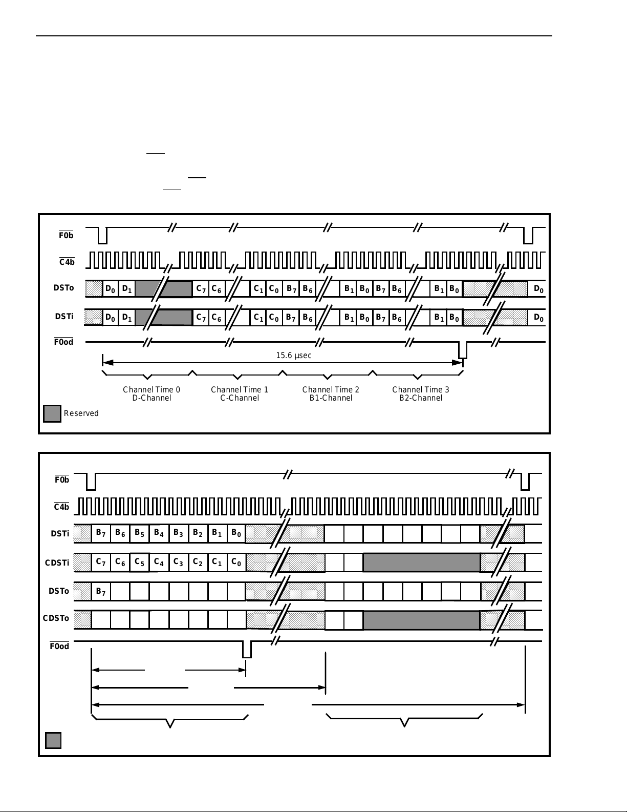
The MT8910-1 has two possible system port
configurations; single port mode or dual port mode.
In the single port mode, the MT8910-1 uses the first
four timeslots of the DSTi and DSTo data streams
(as shown in Figure 8). ST-BUS Channel 0 is
allocated to th e D-ch a n nel, ST-BUS Cha n nel 1 to the
C-channel, while ST-BUS Channel 2 and 3 are
15.6 µsec
6
6
B1B
B1B
0
0
B7B
B7B
6
6
B1B
B1B
0
0
D
0
D
0
F0b
C4b
DSTi
CDSTi
DSTo
CDSTo
F0od
Reserved
AAAA
AAAA
AAAA
AAAA
AAAA
AAAA
AAAA
AAAA
AAAA
AAAA
AAAA
AAAA
AAA
AAA
AAA
AAA
Channel Time 0
D-Channel
Channel Time 1
C-Channel
Figure 8 - ST-BUS Channel Assignments in Single Port Mode
B7B6B5B4B3B2B1B
C7C6C5C4C3C2C1C
B7B6B5B4B3B2B1B
C7C6C5C4C3C2C1C
3.9 µsec
62.5 µsec
Channel Time 2
B1-Channel
0
0
0
0
B7B6B5B4B3B2B1B
D0D
1
B7B6B5B4B3B2B1B
D0D
1
Channel Time 3
B2-Channel
0
0
B
7
C
7
B
7
C
7
125 µsec
9-12
Reserved
Channel Time 0
Channel Time 16
Figure 9 - ST-BUS Channel Assignment in Dual Port Mode
Page 11

Preliminary Information MT8910-1
allocated t o the B1 and B2 channels, respectively. In
this mode, the CDSTi and CDSTo streams are not
used. In the dual port mode, the MT8910-1 uses
both the D STi/DSTo streams a s well as the CDSTi/
CDSTo streams to allow the separation of the data
and control. The two B-channels are routed through
the DSTi/DSTo streams and the C- and D-channels
are routed through the CDSTi/CDSTo streams. In
each case, t imeslot 0 and 16 will carry the respective
channels (refer to Figure 9). To simplify line card
designs, the MT8910-1 provides a delayed frame
pulse (F0od
assignment circuit. This signal is used to drive
subsequent devices in the daisy chain configuration.
In this type of arrangement, only the first MT8910-1
in the chain will receive the system frame pulse (F0b
with the following devices receiving its predecessor's
delayed frame pulse. In conjunction with the delayed
frame pulse, the unused timeslots on the ST-BUS
will be placed into a high impedance state to avoid
having contention on the system bus.
Selecting the single port or the dual port mode is
performed using Mode Select 1 (MS1). With MS1=0,
the DSLIC is in the single port mode while MS1=1
places the DSLIC in the dual port mode. Mode
Select 0 (MS0) determines the order of the D- and Cchannels while the DSLIC is operating in the dual
port mode . W i th MS0 = 0, the C-channel i s f ou nd
in timeslot 0 and the D-channel is found in timeslot
16. With MS0=1, the D-channel is found in timeslot
0 and the C-channel is found in timeslot 16 (refer to
Table 1).
) to eliminate the need for a channel
CRS1 CRS0 Definitio n
0 0 Control Register 1
0 1 Control Register 2
0 0 Control Register 3
11Reserved
The C-channel on the ST-BUS must be continuously
written to every frame. If the user accesses a
Control Register, the information in the other Control
Registers is latched. Any input requested through
the Control Registers will be activated on the next
frame boundary.
Control Register 1
)
Setting CRS0 and CRS1=0 routes the C-channel to
Control Register 1 allowing access to the functions
described in Table 2. These bits are further
described below.
Bits 7 and 6 of Control Register 1, SRS1 & SRS0,
select which status register will be output in the next
ST-BUS frame. The selection of the Status Register
is as follows:
SRS1
0 0 Status Register 1
0 1 Status Register 2
1 0 Status Register 3
1 1 Status Register 4
SRS0 Definition
MS1 MS0
Operating
Dual/Single DC/CD
0 0 Single DC
0 1 Single DC
1 0 Dual CD
1 1 Dual DC
Table 1. Truth Table for M od e Se le ct P in s
Control/Status Channels
The Control and Status information between the
DSLIC transceiver and the controlling entity is
carried by the C-channel. The DSLIC has three input
registers; Control Register 1, 2 and 3 (selected
through the CRS0 and CRS1 bits) and four output
registers; Status Register 1 through Status Register
4 (selected through the SRS0 and SRS1 bits in
Control Register 1).
The input C-channel is used to access Control
Registers 1, 2 and 3. Bit 0 and 1 of the C-channel
(CRS0 and CRS1) allows the selection of the desired
Control Register as described following.
Mode
Bit 5 of Control Register 1, TxSFB, is used to
establish the position of the transmit superframe (LT
mode only). Setting this bit from a logic one to a
logic zero will reset the frame counters on the next
occurrence of the frame pulse establishing the
superframe position. Once the boundaries to the
superframe have been established, the device will
sustain the position of the superframe by allowing
the counters to wrap around. The user can also
elect to set th is b it to a lo g ic ze r o wi th a pe rio d ici ty of
12 ms.
Bit 4 of Control Register 1, BSWAP, allows the
multiplexing of the two B-channels transferred over
the digital subscriber line with the B-channels
presented at the system interface. A logic high on
the bit will result in the B1-channel on the system
interface t o be transmitted in the B2-channel on the
line port and vice versa. The same principle applies
to the B2-channel at the system interface.
Bit 3 of C o nt ro l Register 1, C C RC, allows t he us e r to
introduce errors in the CRC bits calculated by the
DSLIC. This allows the user to verify the error
detection prot ocol used over the M-channel.
9-13
Page 12
MT8910-1 Preliminary Information
Bit 2 of Control Register 1, START/STOP, provides a
mechanism to allow the user to initiate a line
activation or deactivation. This bit is edge sensitive
with a low to high transition requesting an activation,
and a high to low transition requesting a
deactivation. The activation and deactivation
procedure will follow the protocol defined in the ANSI
T1.601-1988. The activation request will only be
recognized if the transceiver is in a full reset state.
Any activ a ti on a tte m p t while the tr a ns ce i ver i s in any
other state will be ignored. Similarly, any
deactivation request generated while the transceiver
is not in the active state will be ignored.
Control Register 2
Setting CRS0=1 and CRS1=0 routes the C-channel
to Control Register 2 allowing access to the
functions described in Table 3. These bits are further
described below.
Bits 7 to 4 of Control Register 2 (DS4 to DS1)
provide access to the multiple diagnostic features
supported on the DSLIC as outlined in Table 3.
These include the per-channel loopbacks at the
system interface as well as a loopback at the line
interface. Along with the extensive loopback
capabilities, the DSLIC also allows the generation of
multiple signals which can be used during
qualification and servicing of a DSL. The isolated
pulse test diagnostics signal causes the transmission
of a +3 or +1 symbol once every 1.5 ms. This will
generate pulses that can be used for template
measurements. The Insertion Loss Measurement
(ILM) test signal is a scrambled all 1s 2B1Q coded
signal which contain both the SW and ISW. This test
signal can be used to make insertion loss
measurements over the DSL loop. Lastly, the DSLIC
can be placed into a quiet mode to allow a Remote
Test Unit (RTU) to perform impulse noise, crosstalk
and other transient impairment measurements as
described in the ANSI "ISDN Management - Basic
Rate Physical Layer".
Bit 3 of Control Register 2 (ADCGAIN) controls the
gain value of the A/D converter. This function can be
used to introduce more gain in t he receive path when
the transceiver is being used over long loops.
Bit 2 of Control Register 2 (MSWAP) may be used
when the DSLIC is operating as an LT within a line
card application. The mode swap feature has the
effect of changing the scrambling polynomial and
activation state machine such that it can simulate the
operation of an NT transceiver. This allows a
transmission test between two devices on the same
line card. (For this function to work properly, the
input clocks to the two devices must be frequency
locked.)
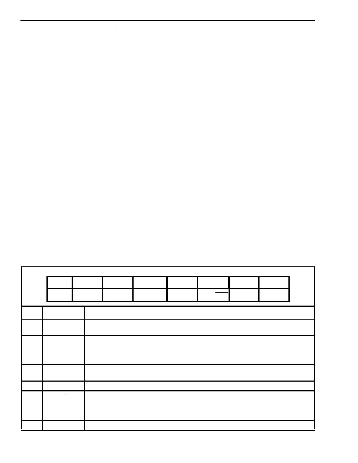
bit 7 bit 6 bit 5 bit 4 bit 3 bit 2 bit 1 bit 0
SRS1 SRS0 TxSFB BSWAP CCRC START/STOP
CRS1 CRS0
Bit Name Descri ption
7,6 SRS1, SRS0 Status Register Select. Selects which of the four status registers will be output in the next ST-
BUS frame.
5 TxSFB Transmit Superframe Reset. In LT mode, transition from a 1 to a 0 on this bit resets the
superframe counters in the next ST-BUS frame in order to establish the transmit superframe
boundary. If the external pin is being used to set the superframe boundary this bit can be held
high or low. Not used in NT mode.
4 BSWAP When this bit is set to 1, the location of the B1 channel o n the ST-BUS is swapped with the
location of the B2 channel. This affects both directions of the ST-BU S.
3 CCRC Corrupt CRC. When set to 1, the 12 bit CRC transmitted on the line is corrupted.
2START/STOP
1, 0 CRS1, CRS0 Control Register Select 1 and 0. Must be set to 0, 0 to address Control Register 1.
A low to high transition while the transceiver is in the full reset state will initiate one activation
attempt. A high to low transition of this bit while the transceiver is in the active state will initiate a
deactivation procedure. During start-up, 2B+D channels should remain set to 0 or 1 until
transparency of network is achieved (indicated by act=1).
Table 2. Con trol Re gist er 1
9-14
Page 13
Preliminary Information MT8910-1
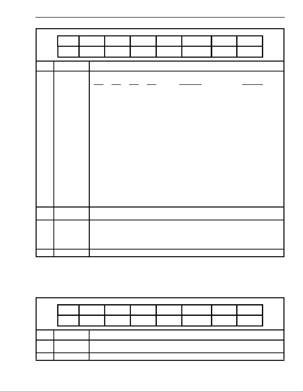
bit 7 bit 6 bit 5 bit 4 bit 3 bit 2 bit 1 bit 0
DS4 DS3 DS2 DS1 ADCGAIN MSWAP CRS1 CRS0
Bit Name Descrip tion
7,6,
5,4
DS4 - DS1 Diagnostic Select Bits.
DS4 DS3 DS 2 DS1 Channels Function
0000 - Normal Operation
0001 B1 STi to STo Loopback
0010 B2 STi to STo Loopback
0011 B1 + B2 STi to STo Loopback
0100 2B + D STi to STo Loopback
0101 B1 STo to STi Loopback
0110 B2 STo to STi Loopback
0111 B1 + B2 STo to STi Loopback
1000 2B + D STo to STi Loopback
1001 ALL L
to Lin Loopback
out
1010 - Isolated +3 pulse
1011 - Isolated +1 pulse
1100 - Transmit 10 kHz Tone
1101 - ILM Test Signal
1110 - Quiet Mode
1111 - Reserved
3 ADCGAIN Selects between two gain values in the delta-sigma A/D converter. When high, selects a 3 dB
higher gain.
2 MSWAP Mode Swap. In the LT mode, MSWAP=1 will result in the DSLIC using the NT’s scrambling/
descrambling polynomials and activation sequence. This allows two DSLICs on the same LT line
card to exchange static data in the B- and D- channels.
1
1
1
1
2
2
2
2
1 3
4
4
5
MSWAP can also be used in the NT mode.
1, 0 CRS1, CRS0 Control Register Select 1 and 0. Must be set to 0, 1 respectively to address Control Register 2.
1
The ST-BUS incoming data is still output on the line if the MT8910-1 is activated. Supported in both SINGLE and DUAL port modes.
2
The incoming data from the line is still output on to the ST-BUS. The other incoming channels on the ST-BUS are still output on to
the line if the d ev ic e is activated. Su pp or te d in bo th S I NGL E and DUA L p o r t m od es .
3
Signal is internally looped back and is still output to the line and overrides the internal activation state machine.
4
One pu ls e is trans m itt ed e ve r y 1. 5 m s .
5
The Insertion Loss Measurement Test Signal is a scrambled (all one’s data), framed 2B1Q signal.
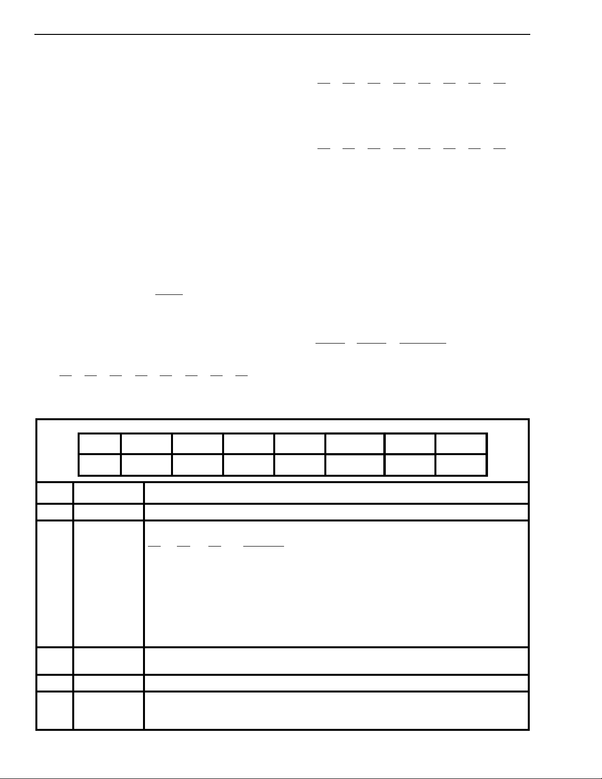
bit 7 bit 6 bit 5 bit 4 bit 3 bit 2 bit 1 bit 0
M1 M2 M3 M4 M5 M6 CRS1 CRS0
Table 3. Con trol Re gist er 2
Bit Name Description
7 - 2 M1 - M6 Tx Maintenance Channel Bits 1 to 6. M-bits which will be transmitted at the end of the next DSL
Basic Frame. Refer to “Maintenance Channel“ section in the functional description
1, 0 CRS1, CRS0 Control Register S elect 1 and 0. Must be set to 1, 0 respectively to address Control Register 3.
Table 4. Con trol Re gist er 3
9-15
Page 14
MT8910-1 Preliminary Information
Control Register 3
Setting CRS1 and CRS0 to 1, 0, respectively, routes
the input C-channel to Control Register 3, allowing
access to the transmit M-bits as shown in Table 4.
The transmit M-channel is a 4 kbit/s maintenance
channel which may carry the EOC messages (with
overhead) as specified in T1.601-1988. Except for
the CRC bits, the M-bits are treated as a transparent
data channel through the DSLIC. CRC bits will be
generated by the transceiver and will be inserted into
the M-channel during their respective M-bit time
slots. (This implies that all input M-bits which are
defined as CRC bits will be overwritten by the
transceiver.) Structuring of the M-bits is described in
the “Maintenance Channel" section of the functional
description.
Control Word s After Rese t
Applying a logic low to the MRST
pin will result in the
three control registers assuming a reset state.
Following a master reset, the three Control Registers
will take th e fo llo w ing s ta te s:
Control Register 1:
C7
C6 C5 C4 C3 C2 C1 C0
00100000
Control Register 2:
C7
C6 C5 C4 C3 C2 C1 C0
00000001
Control Register 3:
C7
C6 C5 C4 C3 C2 C1 C0
11111110
Status Register 1
When SRID1=0 and SRID0=0, the contents of
Status Register 1 are being output in the C-channel
allowing the system to monitor the functions
described below. (Refer to Table 5.)
Bits 7 and 6 of Status Register 1, SRID1 and SRID0,
are used to identify which status register is being
carried in the output C-channel. These bits are
encoded as follows:
SRID1 SR ID0 Definition
0 0 Status Register 1
0 1 Status Register 2
1 0 Status Register 3
1 1 Status Register 4
bit 7 bit 6 bit 5 bit 4 bit 3 bit 2 bit 1 bi t 0
SRID1 SRID0 IS2 IS1 IS0 RxSFIB RSV CRCERR
Bit Name Description
7,6 SRID1, SRID0 Status Register ID. Always reads 0,0 when Status Register 1 is output.
5,4,3 IS2, IS1, IS0 Internal State Indication.
IS1 IS0 Definition
IS2
0 0 0 Full Reset State
0 0 1 Training with no Basic Frame Sync
0 1 0 Training with Basic Frame Sync but no Superframe Sync
0 1 1 Training with Basic Frame Sync and Superframe Sync
1 0 0 Loss of synchronization after E.C. has converged
10 1 NA
1 1 0 Loss of superframe sync after E.C. has converged
1 1 1 Active State
2 RxSFIB Received superframe Indication. When low, indicates the beginning of the received superframe.
This bit is low for one ST- BUS frame, the n high for 95 ST-BUS frames.
1 RSV Reserved. Always read a 0.
0 CRCERR W h en “1”, the received CRC code did not match with a locally generated CRC code, indicating
that the received data included an error. When “0”, the received CRC code matched with the
internally generated CRC.
Table 5. Sta tus Re gist er 1
9-16
Page 15
Preliminary Information MT8910-1
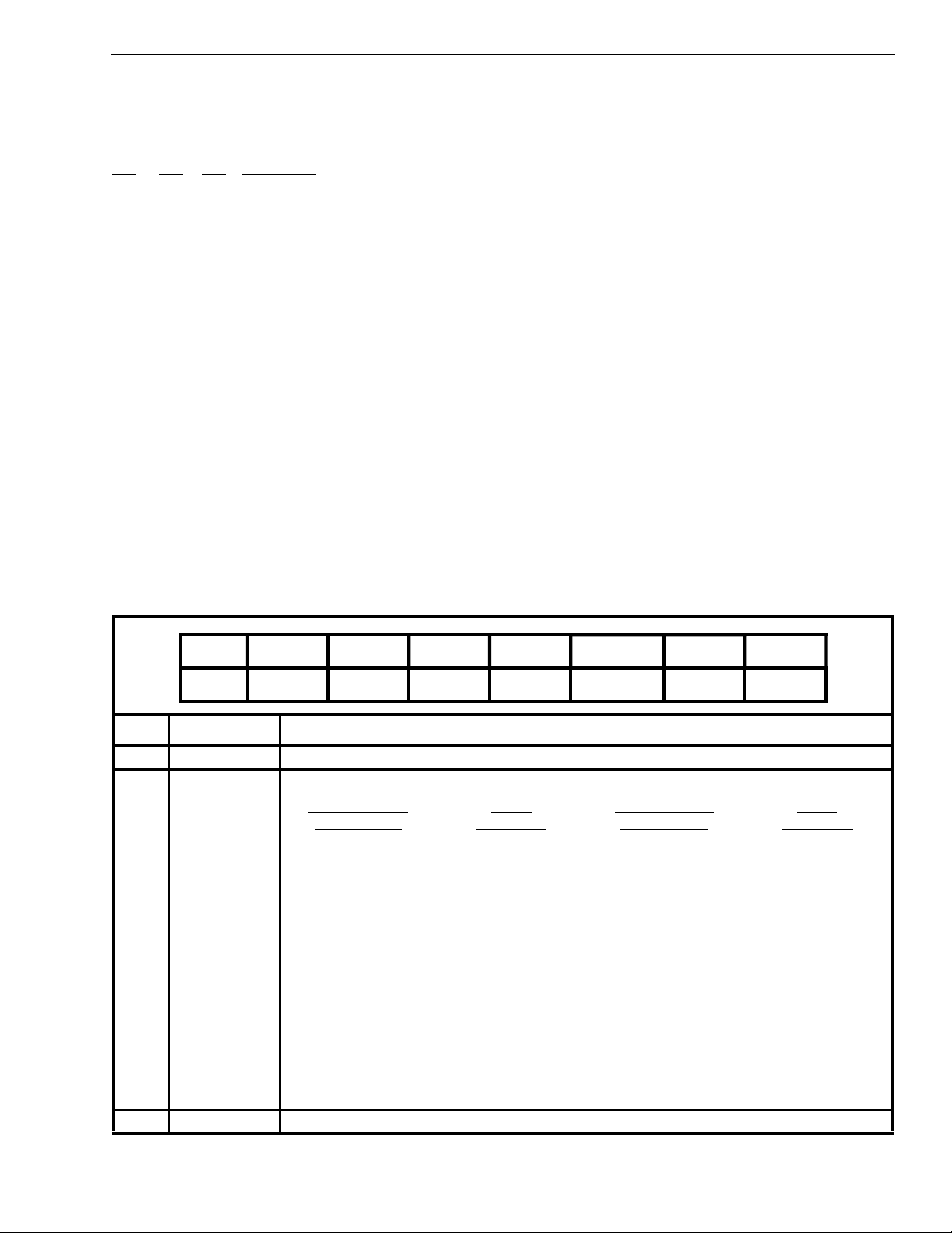
Bits 5, 4 and 3 of Status Register 1, IS2, IS1 and
IS0, provide an indication of the internal state of the
device. The decoded states are as follows:
IS2
IS1 IS0 Definition
0 0 0 Full Reset
0 0 1 Training with n o sync
0 1 0 Training with sync but no
superframe sync
0 1 1 Training with sync and superframe
sync
1 0 0 Loss of sync
101NA
1 1 0 Loss of superframe sync
111Active
Bit 2 of Status Register 1, RxSFIB, is used to
indicate the reception of the receive superframe
boundary in both the LT and NT modes.
Bit 0 of Status Register 1, CRCERR, indicates the
state of the CRC check. A logic high on this bit
states that the CRC check calculated by the
MT8910-1 did not correspond to the CRC bits
received in the M-channel. This bit will only be
updated once every superframe.
Status Register 2
When SRID1=0 and SRID0=1, the contents of Status
Register 2 are being output in the C-channel allowing
the system to monitor the status of the quantizer
signal to noise ratio bits (refer to Table 6). The
QSNR bits reflect the eye closure of the received
signal and represent the signal (+1 symbol) to noise
ratio at the input of the quantizer. This information
can be used to indicate the error performance of the
transceiver. For a more accurate indication of
QSNR, these bits should be averaged over a period
of 64 ST-BUS frames (640 baud). The conversion of
the five bit output to QSNR is shown in Table 6. For
a bit error rate of greater than 10
-7
, the theoretical
QSNR should be greater than 15.7dB.
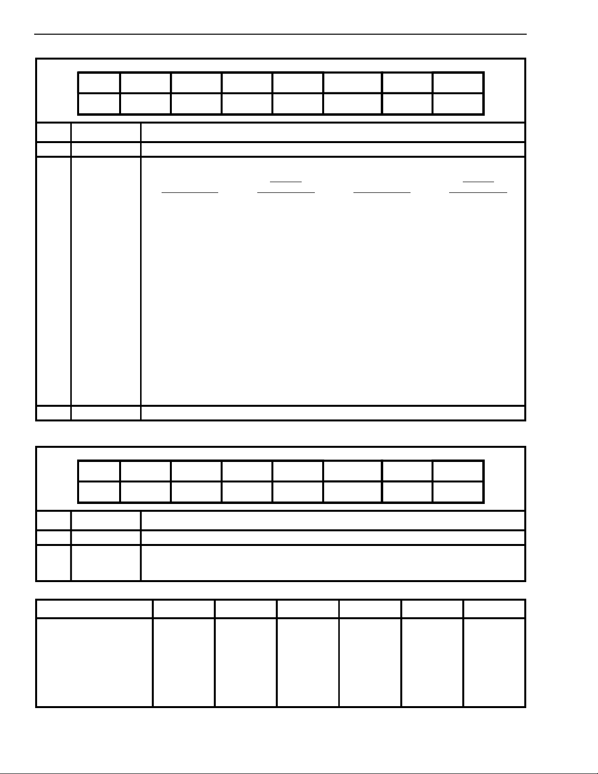
Status Register 3
When SRID1=1 and SRID0=0, the contents of Status
Register 3 are being output in the C-channel allowing
the syst em to monitor the me a n le ve l of the r ec e ive d
symbols (refer to Table 7). The Received Pulse
Amplitude bits (RPA 4 to RPA0) provide an estimate
of the attenuation of the loop. The representation of
the RPA bits is shown in Table 7.
bit 7 bit 6 bit 5 bit 4 bit 3 bit 2 bit 1 bi t 0
SRID1 SRID0 QSNR4 QSNR3 QSNR2 QSNR1 QSNR0 NA
Bit Name Description
7,6 SRI D1, SRID0 Status Register ID. Always reads 0, 1, respectively, when Status Register 2 is output.
5,4,3,
2,1
0 NA Reserved. Always reads 0.
QSNR4,
QSNR3,
QSNR2,
QSNR1,
QSNR0
Quantizer Signal to Noise Ratio Bits. (see Note 1)
QSNR4 (MSB) -
QSNR0 (LSB)
00000
00001
00010
00011
00100
00101
00110
00111
01000
01001
01010
01011
01100
01101
01110
01111
MEAN
QSNR (dB)
>36.1
36.1
30.1
26.6
24.1
22.2
20.6
19.2
18.1
17.1
16.1
15.3
14.6
13.9
13.2
12.6
QSNR4 (MSB) -
QSNR0 (LSB)
10000
10001
10010
10011
10100
10101
10110
10111
11000
11001
11010
11011
11100
11101
11110
11111
Table 6. Sta tus Re gist er 2
Note 1) N o t P roduction Tested
MEAN
QSNR( dB)
12.1
11.5
11.0
10.6
10.1
9.7
9.3
8.9
8.5
8.2
7.9
7.5
7.2
6.9
6.6
6.3
9-17
Page 16
MT8910-1 Preliminary Information
bit 7 bit 6 bit 5 bit 4 bit 3 bit 2 bit 1 bi t 0
SRID1 SRID0 RPA4 RPA3 RPA2 RPA1 RPA0 RSV
Bit Name Description
7,6 SRI D1, SRID0 Status Register ID. Always reads 1, 0, respectively, when Status Register 3 is output.
5,4,3,
2,1
0 RSV R eserved. Always reads 0.
Note 1) N o t P roduction Tested
RPA4-RPA0 R eceive Pulse Amplitude bits (see Note 1).
Relative
RPA4 - RPA0
0 0 0 0 0
0 0 0 0 1
0 0 0 1 0
0 0 0 1 1
0 0 1 0 0
0 0 1 0 1
0 0 1 1 0
0 0 1 1 1
0 1 0 0 0
0 1 0 0 1
0 1 0 1 0
0 1 0 1 1
0 1 1 0 0
0 1 1 0 1
0 1 1 1 0
0 1 1 1 1
Notes: Loop leng th c an be calculated by di vi di ng R e ce iv e Pulse Amp li tud e (RPA) by the ty pical
cable a ttenuation fo r a 2 B1Q pu ls e.
Relativ e am p litude is ba s ed on R PA read in g o f z e r o lin e length with r e co m me n de d
termin at ion a nd tr a n sfo rm er (AD C Ga in = 0).
Amplitude (dB)
-31.85
-30.10
-28.65
-27.41
-25.83
-24.08
-22.63
-21.39
-19.80
-18.06
-16.61
-15.37
-13.78
-12.04
-10.59
-9.35
Table 7. Sta tus Re gist er 3
RPA4 - RPA0
1 0 0 0 0
1 0 0 0 1
1 0 0 1 0
1 0 0 1 1
1 0 1 0 0
1 0 1 0 1
1 0 1 1 0
1 0 1 1 1
1 1 0 0 0
1 1 0 0 1
1 1 0 1 0
1 1 0 1 1
1 1 1 0 0
1 1 1 0 1
1 1 1 1 0
1 1 1 1 1
Relative
Amplitude (dB)
-7.76
-6.02
-4.57
-3.33
-1.74
0
1.45
2.69
4.28
6.02
NA
NA
NA
NA
NA
NA
bit 7 bit 6 bit 5 bit 4 bit 3 bit 2 bit 1 bi t 0
SRID1 SRID0 M1 M2 M3 M4 M5 M 6
Bit Name Description
7,6 SRI D1, SRID0 Status Register ID. Always reads 1, 1, respectively, when Status Register 4 is output.
5,4,3,
2,1,0
M1 - M6 Rx Maintenance Channel Bits 1 to 6. M-bits which were received at the end of the last DSL Basic
Frame. Refer to the "Maintenance Channel" section in the functional description for the
structuring of the received M-bits.
Table 8. Sta tus Re gist er 4
ST-BUS Frame Access M1 M2 M3 M4 M5 M6
0 - 9
12 -21
24 - 33
36 - 45
48 - 57
60 - 69
72 - 81
84 - 93
M11
M12
M13
M14
M15
M16
M17
M18
M21
M22
M23
M24
M25
M26
M27
M28
M31
M32
M33
M34
M35
M36
M37
M38
M41
M42
M43
M44
M45
M46
M47
M48
M51
M52
CRC1
CRC3
CRC5
CRC7
CRC9
CRC11
M61
M62
CRC2
CRC4
CRC6
CRC8
CRC10
CRC12
Table 9. Maintenance Channel Bit Assignment on ST-BUS Port
9-18
Page 17
Preliminary Information MT8910-1
Status Reg ister 4
When SRID1=1 and SRID0=1, the contents of the
Status Register 4 are being output in the C-channel
allowing the system to monitor the received
maintenance channel bits M1 to M6 as specified in
Table 8. The received M-bits may carry the EOC
message (with overhead) as specified in T1.601-
1988. Refer to the “Maintenance Channel“ section
for further details.
Maintenance Channel
The MT8910-1 has provisions for transmitting and
receiving a 4 kbit/s maintenance channel from the
system port to the line port. The maintenance
channel at the line port is structured into six columns
of which M5 and M6 carry the results of a CRC
calculation (refer to Table 9). All bits except these
CRC bits are trea te d a s a transparent chan n el to the
MT8910-1. The 12 bit cyclical redundancy check is
computed using the generator polynomial:
12
11
⊕
x
(where
⊕ x
⊕ is modulo two summation)
x3 ⊕ x2 ⊕ x ⊕ 1
bits for all DSL basic frames are written to Control
Register 3 once every 1.5ms within the ST-BUS
frames indicated in Table 9. If the user fails to
update the contents of Control Register 3 within the
allocated window, the M-bits will be substituted by
ones until the information in Control Register 3 is
updated. On the receive path, the Rx M-bits from
each DSL basic frame are available in Status
Register 4 within the ST-BUS frames indicated in
Table 9. The Rx M-bits will be updated every DSL
basic frame (or 1.5 ms).
The M-bits are structured according to the transmit
and receive superframe boundary signals output on
the ST-BUS. The transmit superframe boundary is
defined relative to the input or output SFb
signal. ( In
LT mode, the transmit superframe boundary can also
be defined in the frame followi ng the TxSFB bit being
set to zero.) The ST-BUS frame in which the SFb
signal is active is defined as transmit frame 0. The
superframe boundary in the receive path is defined
relative to the RxSFIB bit found in Status Register 1.
The ST-BUS frame with RxSFIB=0 is defined as the
receive frame 0. The functional timing diagram for
the phase of the SFb and RxSFIB signals for both
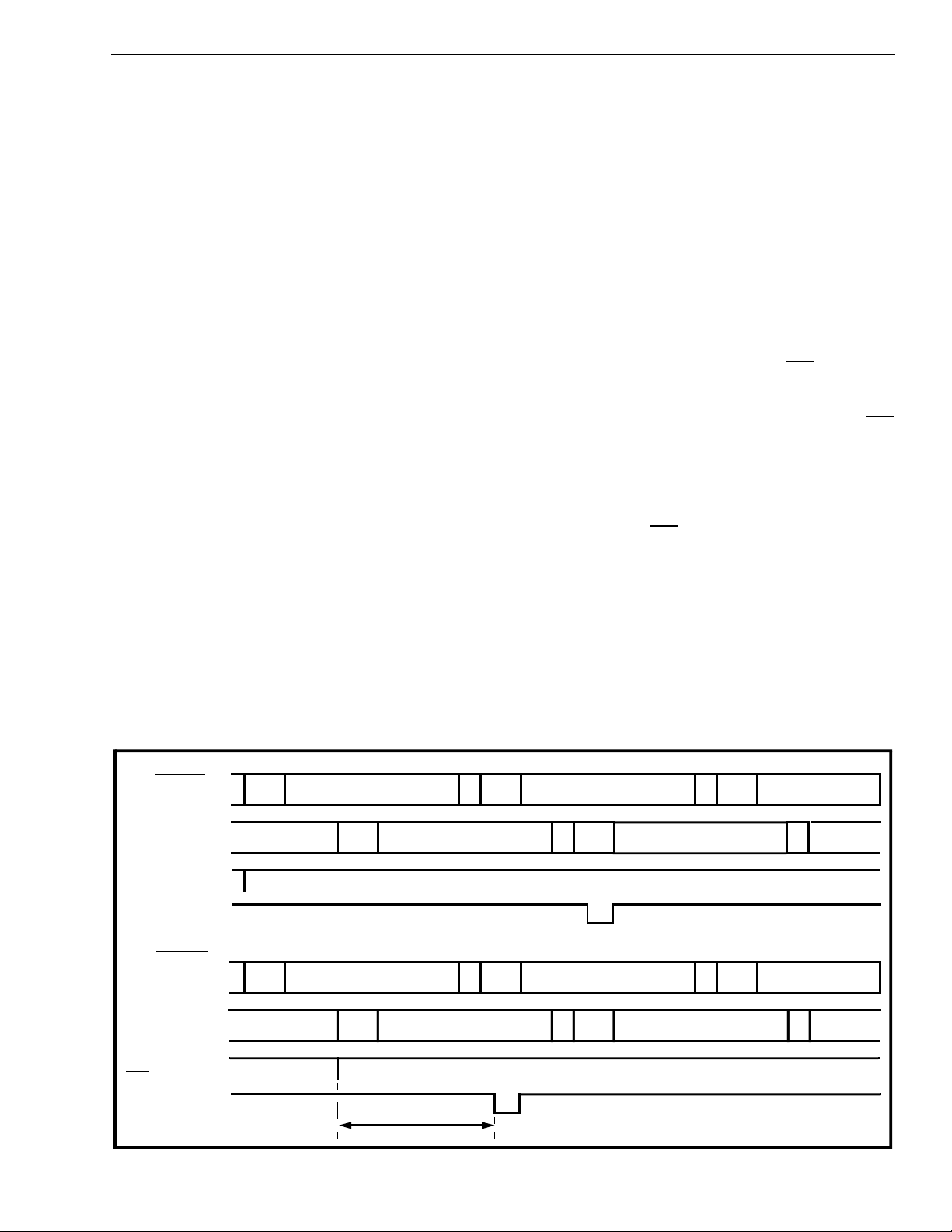
the LT and NT modes is shown in Figure 10.
The CRC calculation covers all 2B + D-channels
within a superframe as well as the M4 column within
the maintenance channel.
Access to the maintenance channel is granted
through Control Register 3 (Tx M-Channel) and
Status Register 4 (Rx M-Channel) and is structured
on the ST-BUS port as shown in Table 9. The Tx M-
LT Mode
Tx Line Signal
Rx Line Sigmal
pin
SFb
RxSFIB bit
NT Mode
Rx Line Signal
Tx Line Signal
ISW 12x(2B + D) M SW 12x(2B + D) M SW 12x(2B + D)
ISW 1 2x(2B + D) M SW 12x(2B + D) M
ISW 12x(2B + D) M SW 12x(2B + D) M SW 12x(2B + D)
ISW 12x(2B + D) M SW 12x(2B + D) M
In applications which do not utilize the maintenance
channel, 2B+D data at the NT and the LT should be
all set to 0 or 1 until activation occurs at the LT.
Since the NT trains up before the LT, the activation at
the LT can be detected at the NT by the reception of
random data. Only then the NT can transmit normal
2B+ D dat a.
SFb
pin
RxSFIB bit
7 ST-BUS Frames
Figure 10 - Functional Timing for Superframe Signals
9-19
Page 18
MT8910-1 Preliminary Information
10.24 MHz Clo ck Inte rfa ce
The MT8910-1 can operate either with an external
clock or with a built-in oscillator clock using a 10.24
MHz parallel resonance crystal. While using the
external clock, the timing relationship between C4b
and the external clock should be as shown in Figure
15. This is typically used in LT mod e. To meet the
specified line performance, the tolerance of the
external clock should be ±5ppm. In NT mode, the
MT8910-1 can use the built-in crystal oscillator
circuit for internal timing, and to meet the specified
line performance, the tolerance of the crystal is
specified to be ±50ppm.
The oscillator in the MT8910-1 uses the Pierce
circuit configuration. In this type of oscillator, the
necessary phase shift is obtained by the two
components connected in series; one of them is the
crystal itself, and the other is the RC combination of
the output impedance of the inverter and the
capacitor connected to its output and the ground.
This requires the output impedance of the inverter to
be high for minimizing the power consumption of the
MT8910-1. When OSC1 is used as an input for an
external clock (typically in LT mode), the high output
impedance of the inverter coupled with any stray
capacitance on the OSC2 pin can distort the
waveform and change the duty cycle of the clock
signal fed to the internal blocks of the MT8910-1.
This may result in improper operation. Hence, it is
recommended that an external inverter be connected
in parallel strengthening the internal inverter as
shown in Figure 11.
I/O Structu re Test
The MT8910-1 has a built-in test structure that
allows verification of all digital I/O structures. The “I/
O Structure Test“ is a static test designed to allow a
parity check on all digital inputs, force all digital
output drivers to any state as well as placing all
digital outputs into a high impedance state. These
three variables can be used to verify the integrity of
the connections between the MT8910-1 and the
printed circuit board.
The I/O structure test has three dedicated pins which
are used to; enable the test structure (TSTen),
provide an output (TSTout) of an XOR chain that is
used to verify all digital input pins, as well as
providing an input signal (TSTin) to all output drivers.
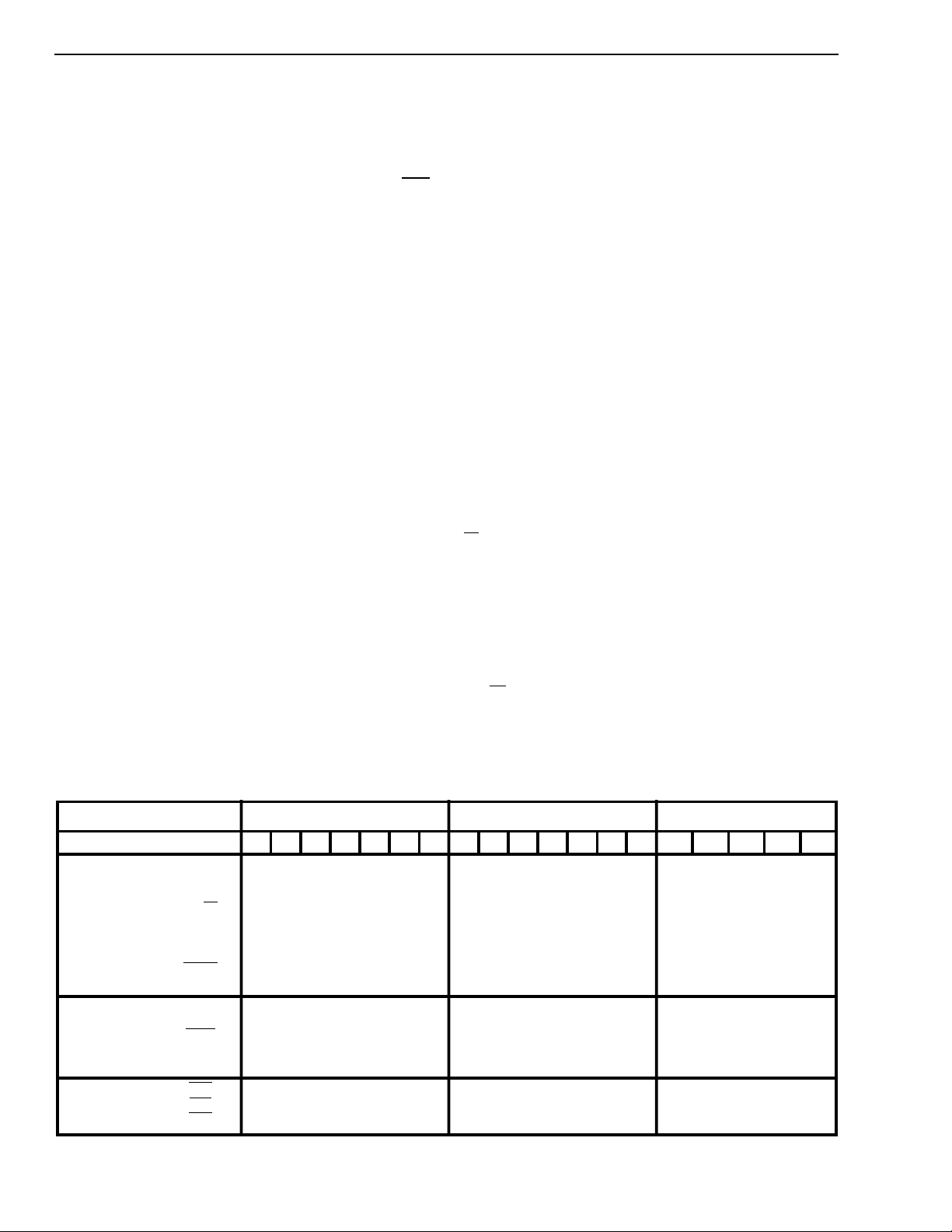
Before enabling the test structure, the default I/O
structure must be cleared to avoid interference with
the test results. This can be accomplished by
inserting the test vectors as defined in Table 10
below. Once the initialization procedure has been
run, the respective testing mode can be enabled
using the three mode select pins MS0, MS1 and NT/
LT
.
The I/O structure test allows the verification of the
connection between the printed circuit board and the
digital input pins to the MT8910-1. After running the
initialization sequence described above, the I/O input
structure test can be enabled by setting TSTen to a
logic high with the mode select pins MS0, MS1 and
NT/LT set to 1, 0, 1 respectively. This forces all
digital input s to be linked into an XOR chain whose
output drives the I/O structure test output (TSTout)
1
pin
. The TSTout pin will carry the output of the XOR
comparison from signals on pins, CDSTi, DSTi,
Initialization Input Tests Output Tests
Time Stamp (e.g.: 1 µs) 1 2 3 4 5 6 7 8 9 10 11 12 13 14 15 16 17 18 19
Input
Signals
Output
Signals
Bidirectional
Signals
TSTen
MS0
MS1
NT/LT
TSTin
CDSTi
DSTi
MRST
OSC1
DSTo
CDSTo
F0od
OSC2
TSTout
C4b
F0b
SFb
0
0
0
0
0
0
0
0
0
0
0
0
0
0
0
1
0
X
X
X
X
X
X
X
X
X
X
1
0
0
0
0
0
0
0
0
0
0
0
0
0
0
0
0
0
0
0
0
0
X
X
X
X
X
X
X
X
X
X
0
0
1
0
0
0
0
0
0
0
0
0
0
0
0
0
0
0
0
0
0
0
X
X
X
X
X
X
X
X
X
X
0
1
1
1
0
0
1
0
0
0
1
0
0
0
0
0
0
0
0
0
0
0
X
X
X
X
X
X
X
X
L
X
0
1
0
0
0
0
•
1
•
0
•
1
•
0
•
1
•
0
•
0
•
0
•
X
•
X
•
X
•
X
•
H
•
0
•
0
•
0
•
•
•
•
•
•
•
•
•
•
•
•
•
•
•
•
•
•
•
•
•
•
•
•
•
•
•
•
•
•
•
•
1
1
0
0
1
1
0
0
0
0
0
0
0
0
0
0
X
X
X
X
X
X
X
X
H
L
0
0
0
0
1
0
1
0
1
0
0
0
0
0
0
0
0
0
0
0
1
0
0
X
0
X
0
X
0
X
0
X
0
X
0
X
0
X
1
1
1
1
0
0
0
1
0
0
0
0
0
0
1
0
0
1
0
1
0
1
0
1
0
1
0
1
0
1
0
1
1
1
1
0
1
1
•
•
•
1
1
0
0
0
0
0
0
Table 10. I /O Str uctu re Test Vectors
X=Don’t C a re Z=H igh Im p ed an c e S t at e
9-20
1
1
0
0
0
0
0
0
0
Z
Z
Z
1
Z
Z
Z
Z
Page 19
Preliminary Information MT8910-1
V
DD
0.1µF
0.1µF
M
H
8
9
1
0
1
PL T
TO NEXT DSLIC
1:1.3
1.0µF1.0µF
IN CHAIN
1.5µF
TO LINE FEED
SUPPLY
*Duty cycle: 45% to 55%
74HC04
10.24 MHz Clock
74HC04
*
4.096 MHz Clock
8 kHz Frame Pulse
12ms Superframe Pulse
PCM or Data In
PCM or Data Out
System
Reset
20
19
17
18
16
12
13
14
15
21
6
8
4
5
7
3
OSC1
OSC2
C4b
F0b
SFb
DSTi
DSTo
MS0
MS1
NT/LT
TSTin
TSTen
CDSTi
MRST
VSS
AVSS
MT8910-1
VDD
AVDD
Lout+
Lin+
Lin-
Lout-
VBias
VRef
CDSTo
TSTout
F0od
22
1µF
24
1µF
2
28
27
1
25
26
9
23
IC
11
10
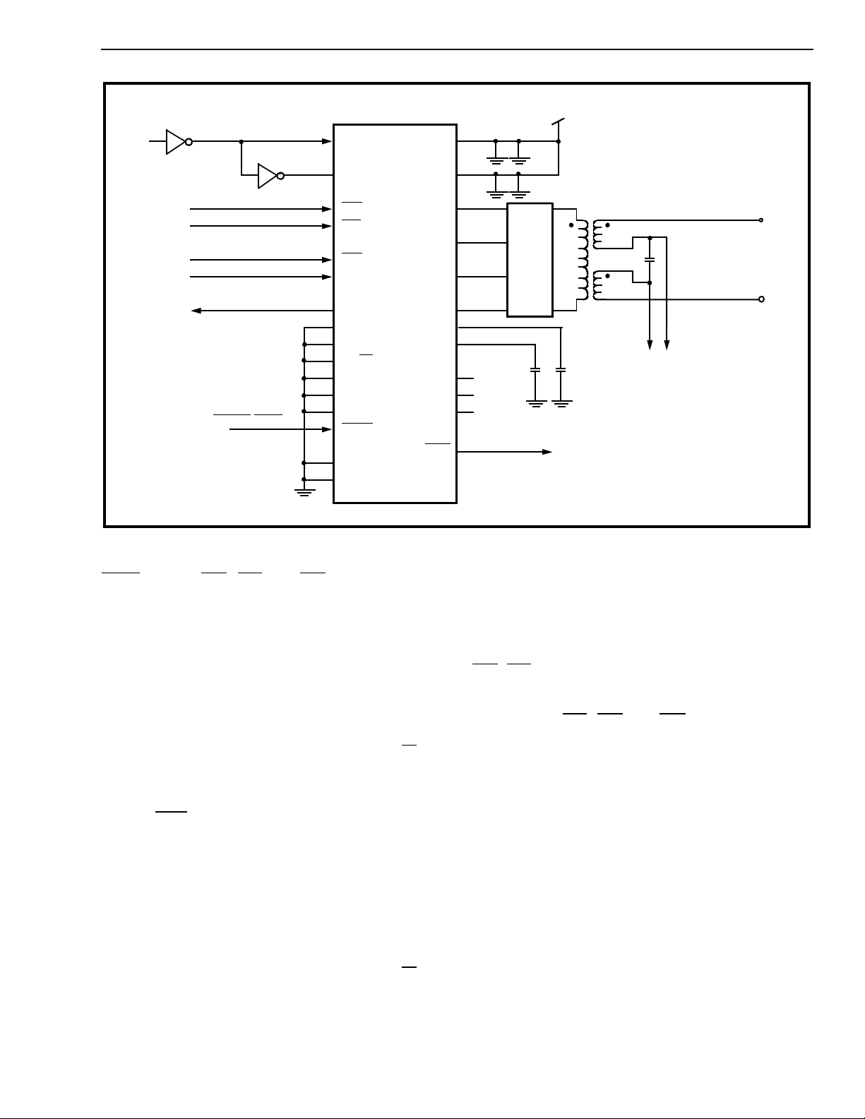
Figure 11 - Typical Connections for LT Mode (Single Port)
MRST, OSC1, C4b, F0b and SFb. TSTout=0 if all
input signals carry an even number of ones and
TSTout=1 if all input signals carry an odd number of
ones.
The I/O structure test also allows the verification of
the connection between the digital output pins and
the printed circuit board. After running the
initialization sequence, the I/O structure output test
can be enabled by setting the TSTen to a logic high
with the mode select pins MS0, MS1 and NT/LT
set
to 1, 1, 0 respectively. This causes all digital outputs
to be drive n from th e I/O stru cture test input (T STin)
pin1. The outputs affected include the DSTo,
CDSTo, F0od
and TSTout
These same outputs can also be placed into a high
impedance state to allow the bed-of-nails tester or
some other in-circuit tester to drive a known signal or
pattern on any circuitry that may be connected to the
output pins of the MT8910-1. The high impedance
state is enabled by running the initialization pattern
described above then setting TSTen to a logic one
with the mode select pins MS0, MS1 and NT/LT
set
to 1, 0, 0 respectively.
Applications
The typical connection diagrams are shown in
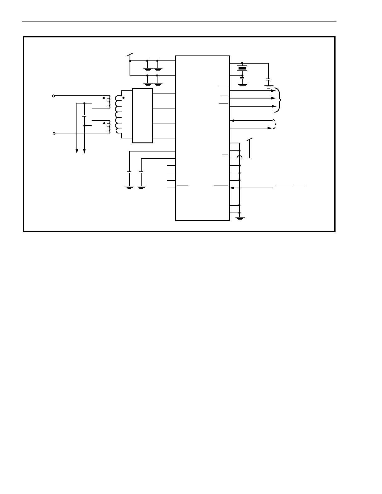
Figures 11 and 12. In Figure 11, the MT8910-1
receives all its timing from the system including the
C4b
, F0b and a frequency-locked 10.24 MHz master
clock. In Figure 12, the MT8910-1 is configured in
the NT mode which implies that all timing signals
including the F0b
from the MT8910-1. These timing signal are
generated from an internal DPLL which divides a
10.24 MHz reference frequency down to a baseband
160 kHz. A comparison is performed on the
reference signal with the received line signal to
determine if the timing signals on the MT8910-1
have to be c o rr ec te d .
The MT8910-1 is interfaced to the transmission line
through the Passive Line Termination network (PLT)
and transformer. The PLT provides the two to four
wire conversion and additional frequency
compensation for the received signal. The whole
circuit is DC isolated from the line by the low
inductance transformer.
, C4b and SFb are being sourced
Note 1: Allow a propagation delay of approximately 800ns
from digital input to XOR output or TSTin to any
digital output.
9-21
Page 20
MT8910-1 Preliminary Information
V
1.5µF
TO DC-DC
CONVERTER
DD
0.1µF
0.1µF
PLT
22
1µF
24
1µF
2
M
H
8
9
1
0
1
1.0µF1.0µF
28
27
1
25
26
9
23
11
10
VDD
AVDD
Lout+
Lin+
Lin-
Lout-
VBias
VRef
CDSTo
IC
TSTout
F0od
MT8910-1
OSC1
OSC2
C4b
F0b
SFb
DSTi
DSTo
MS0
MS1
NT/LT
TSTin
TSTen
CDSTi
MRST
20
10.24 MHz
19
17
18
16
6
8
12
13
14
4
15
5
Xtal
33pF
V
DD
21
33pF
CLOCKS
PCM OR
DATA
System Reset
Figure 12 - Typical Connections for NT Mode (Single Port)
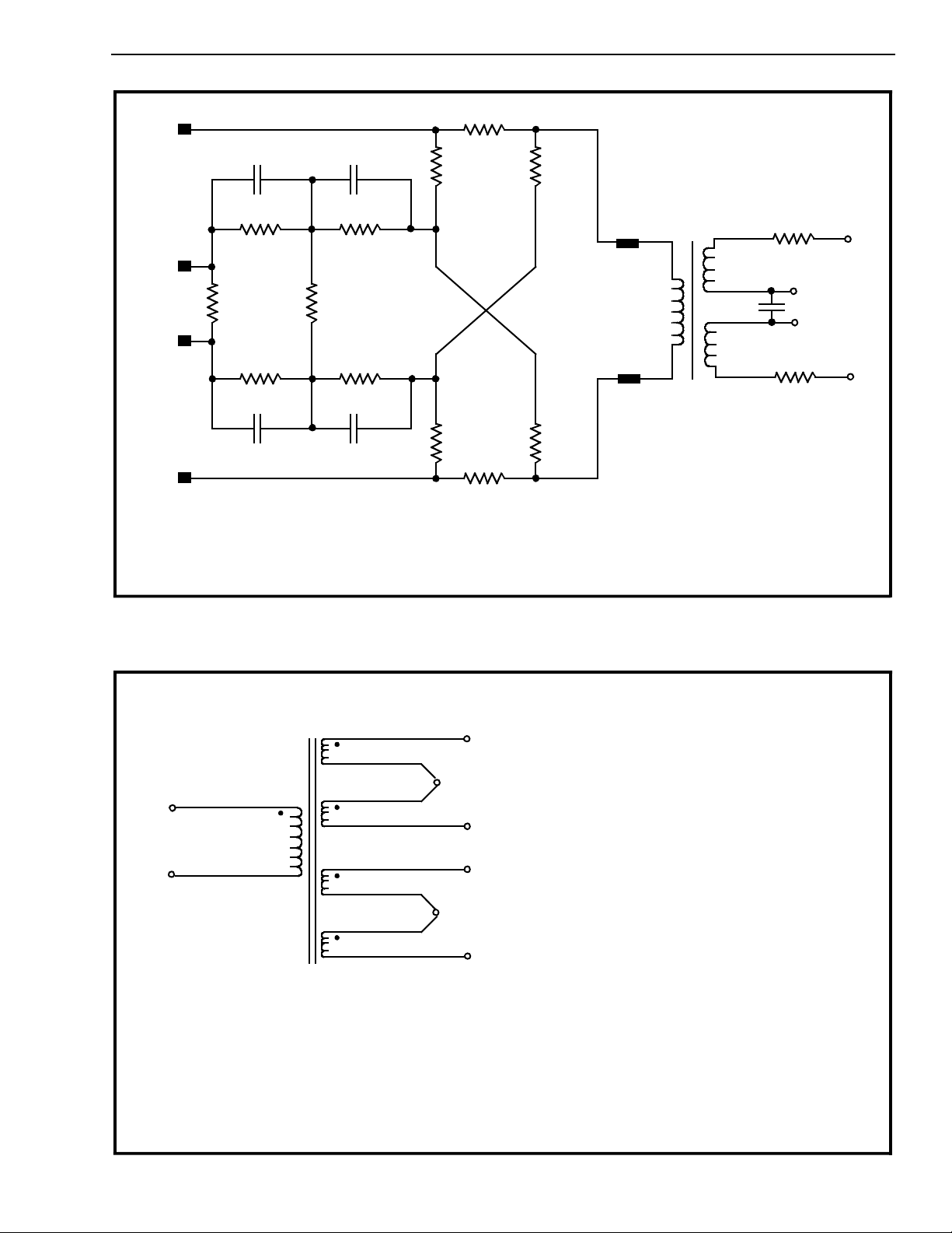
Passive Line Termination Network (PLT)
The termination network is an all passive circuit
which allows the MT8 910-1 to interfac e to the DSL
line through a line pulse transformer. The passive
line termination consists of three blocks which
includes a hybrid network, a compensator circuit and
a line pulse transformer (refer to Figures 13 and 14).
The hybrid network is a 2 to 4 wire converter which
provides limited precancellation of near end echo.
The hybrid specified in Figure 13 was optimized for
the specified transformer and a 10 ohm series
protection resistor (Rp).
The compensator circuit, in conjunction with the
transformer, acts as a high pass filter which is
designed to increase the cut-off frequency in the
receiver path. This has the eff ect of reducing the low
frequency content in the received line signal which in
turn reduces the effects of ISI and near end echo
thereby improving transceiver performance.
7
VSS
AVSS
3
Transformer Specificat io n
All subscriber equipment which is to be connected to
a digital subscriber line, must deliver an output pulse
which satisfies both the pulse template and the pulse
PSD as specified earlier. The output drive
characteristics of the MT8910-1 requires a
transformer with a turns ratio of 1:1.3 having the
electrical characteristics specified in Figure 14.
For supporting initial design activities, Mitel
Semiconductor has made available the MB6024
Magnetic Kit which contains the transformer shown
in Fig. 14.
The low inductance transformer allows for the
possibility of passing a sealing current and/or
phantom feed supply through the secondary winding
without saturating the magnetic core. The
transformer specified in Figure 14 has been
designed to carry typically 50 mA of DC current.
9-22
Page 21
Preliminary Information MT8910-1
= 30.2 Ω
R
L
+
out
680 pF
3.3 nF
s
R
b1
1.6 KΩ
R
b2
1 KΩ
XFM+
1:1.3
130 KΩ 20 KΩ
+
L
in
68.2 KΩ
L
-
in
130 KΩ
7.8 KΩ
20 KΩ
7 mH
5.5 mH
1.5 µF
5.5 mH
XFM-
R
b1
680 pF
-
L
out
3.3 nF
1.6 KΩ
R
b2
1 KΩ
Rs = 30.2 Ω
Note 1: All resistors have a tolerance of ±1% unless indicated otherwise. All capacitors have a tolerance of ±10%.
Note 2: May be incorporated on to a ceramic substrate.
Figure 13 - Passive Line Termination (PLT)
10 Ω ±10%
Power
Feed/Extract
10 Ω ±10%
➃
8
5
NOTES: ➀ Open Circuit Secondary
② Open Circuit Primary
➂ With pins 1 and 11 shorted together
➃ Filtran Part Number TPW 4671
2
7
11
1
6
TURNS RATIO
RESISTANCE
INDUCTANCE
Leakage Inductance (Sec. Short Circuit) < 75µH @ 40 kHz.
LONGT. BAL.
0 - 4 kHz
4-160 kH z
12
Figure 14 - Transformer Specification
1:1.3
R
= 5-8 3.7 Ω
1
R
= 2-12 6.8 Ω
2
= 5-8 7 mH
L
P
= 2-12 11 mH
L
S
min 63 dB
min 58 dB
➂
➀
②➂
9-23
Page 22
MT8910-1 Preliminary Information
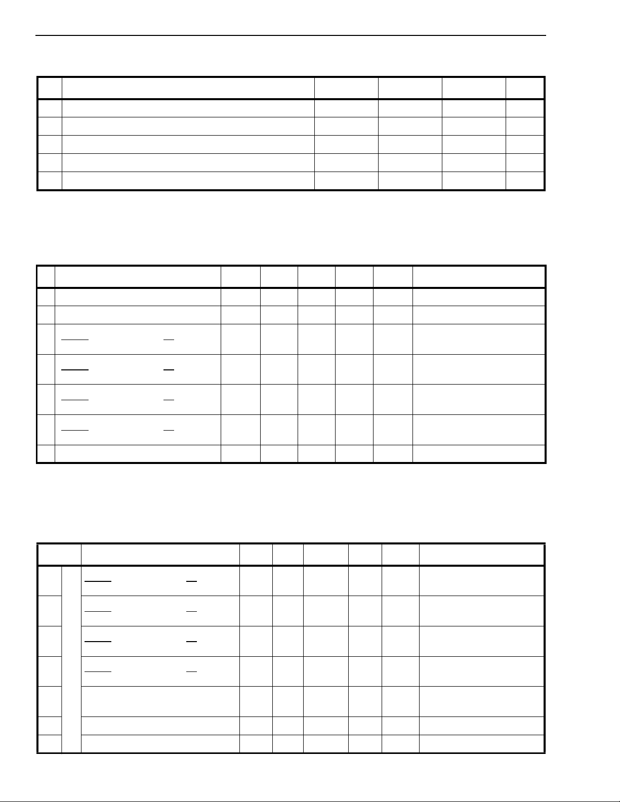
Absolute Maximum Ratings*
Parameters Symbol Min Max Units
1 Supply Voltage V
2 Voltage on any I/O pin V
3 Current on any I/O pin I
4 Storage Temperature T
5 Package Power Dissipation P
Exceeding these values may cause permanent damage. Functional operation under these conditions is not implied.
Note 1: Exce pt fo r VDD, AVDD, VSS, AVSS, L
out+
and L
out-
.
DD
I/O
I/O
ST
D
Recommended Operating Conditions - Voltages are with respect to ground (V
Characteristics Sym Min Typ
1 S upply Voltage V
2 Analog Supply V oltage AV
DD
4.75 5.00 5.25 V (see Note 1)
4.75 5.00 5.25 V Relative to AVSS (Note 1)
DD
‡
Max Units Test Conditions
-0.3 7.0 V
-0.3 VDD +0.3 V
-55 1 25 °C
) unless otherwise stated.
SS
3 Input Low Voltage (except OSC1,
MRST
, MS0, MS1, NT/LT V
IL
0.4 for 400mV noise margin
4 Input High Voltage (except OSC1,
MRST
, MS0, MS1, NT/LT V
IH
2.4 V for 400mV noise margin
5 Input Low Voltage for OSC1/2,
MRST
, MS0, MS1, NT/LT V
IL
1.0 V
6 Input High Voltage for OSC1/2,
MRST
, MS0, MS1, NT/LT V
7 Operating Temperature T
‡ Typical figures are at 25°C and are for design aid only: not guaranteed and not subject to producti on testing.
IH
A
4.0 V
070°C
20 mA
1000 mW
Note 1: To obtain optimum lin e pe r fo rm ance, noi se l ev el on s up pl y m us t be less th an 2 5 m Vp p.
DC Electrical Characteristics - Voltages are with respect to ground (V
Characteristics Sym Min T yp
1
Input High Voltage (except OSC1,
, MS0, M S1, NT/LT V
MRST
2.0 V
IH
‡
) unless otherwise stated.
SS
Max Units Test Conditi ons
2 Input Low Voltage (except OSC1,
MRST
, MS0, M S1, NT/LT V
I
3 I nput High Voltage for OSC1/2,
N
MRST
P
4 I nput Low Voltage for OSC1/ 2,
U
T
S
5 I nput Leakage Current (except
, MS0, M S1, NT/LT V
MRST
, MS0, M S1, NT/LT V
IL
3.0 V
IH
IL
I
10 µA V
IL
0.8 V
2.0 V
OSC1)
6 I nput Current for OSC1 I
7 I nput Im pedan ce (L
in-
to L
)Z
in+
IC
in
50 100 µA V
250 kΩ @ DC
= VSS to V
IN
= VSS to V
IN
DD
DD
9-24
Page 23
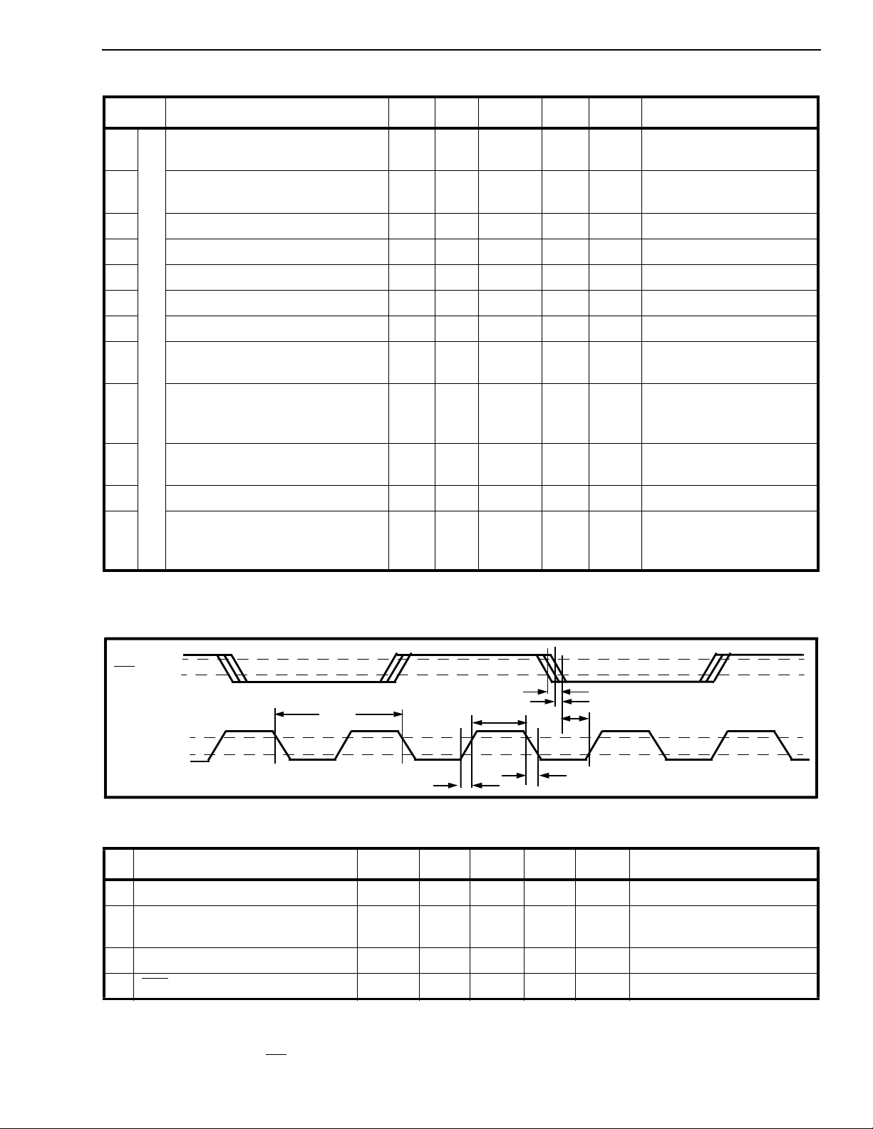
Preliminary Information MT8910-1
DC Electrical Characteristics (continued) - Voltages are with respect to ground (V
0.5AV
‡
Max Units Test Conditi ons
DD
V Relative to AV
Characteristi cs Sym Min Typ
8
V
Voltage V
Bias
Bias
) unless otherwise stated.
SS
SS
CL=1 µF minimum to AV
9V
Voltage V
Ref
Ref
-1.9 V Relative to V
Bias
CL= 1µF minimum to AV
10 V
11 Output High Voltage
12 Output Low Voltage
O
13 OSC2 Output High Voltage V
U
14 OSC2 Output Low Voltage V
T
P
15 Differential Output Voltage
U
T
16 Output Impedance
S
(L
(L
Bias
out+
out+
and/or V
to L
out-
, L
out-
load V
Ref
(1)
(1)
)V
)Z
V
V
BL
OH
OH
OL
out
out
1MΩ(see Note 2)
2.4 V IOH=10mA
OL
0.4 V IOL= 5.0mA
3.5 V IOH=10µA
1.5 V IOL=10µA
6.4 V
pp
RL=40Ω
Measured by sourcing and
0.5 Ω
sinking 10 mA. Line Driver
active.
17 Output Capacitance
, L
(L
out+
)C
out-
18 High Impedance Leakage I
19 Supply Current I
o
OZ
DD
65
50 pF (see Note 1)
10 µA
mAmALine Drivers active and
unloaded.
I
DD
‡ Typical figures are at 25°C and are for design aid only: not guaranteed and not subject to producti on testing.
1
) except OSC2
(
Note 1) This is a sp e ci fic at ion on the m a xi mu m pa r a lle l ca pa ci tance to AC g rou nd, conn ec te d d ire c t ly to the pi ns . H ig he r
capacit ance is ac ce ptable whe n placed in s eri es w i th r es is to r n etworks s uc h a s the line term i nation im pe da nc e .
2) Not production tested.
10
Low Power Mode
SS
SS
V
C4b
OSC2
IH
V
IL
t
MCF
V
IH
V
IL
t
OCT
t
OCH
t
JC
t
OCT
t
JC
(See Note 3)
Figure 15 - Ex ter na l Clo ck Timi ng i n LT Mode
AC Electrical Characteristics†- External Clock Timing (Ref. Figure 15)
Characteristics S ym M in Typ
1 OSC2 Clock Frequency 1/t
2 OSC2 Clock Duty Cycle t
3 OSC2 Clock Transition Time t
4C4b
† Timing is over recommended temperature & power supply voltages.
‡ Typical figures are at 25°C and are for design aid only: not guaranteed and not subject to producti on testing.
Notes: 1) External clock t olerance of ±5 ppm in LT mode o r ±5 0 ppm in NT mode i s req uired.
Jitter (wrt OSC2) t
2) Absolute jitter on OSC2 must be less than 2.0ns RMS in order to maximize performance.
3) In LT mode the C4b
between th e cl oc k s is no t c rit ic al .
and OSC2 clocks must be externally frequency locked (i.e., f
MCF
OCH
t
MCF
OCT
JC
/
45 50 55 %
-15 +15 ns (see Note 3)
‡
Max Uni ts Test Conditions
10.24 MHz (see Notes 1, 2 & 3)
10 ns
= 2.5 x f
OSC2
). The relativ e ph as e
C4b
9-25
Page 24
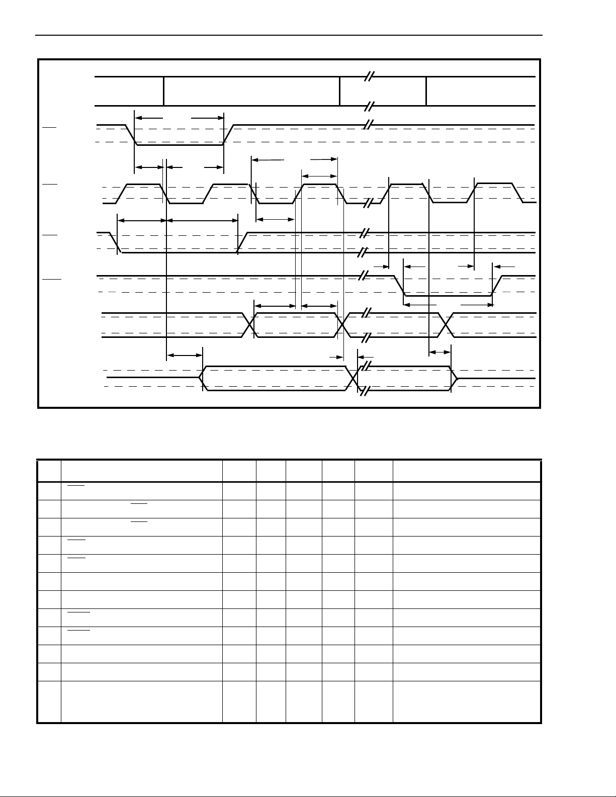
MT8910-1 Preliminary Information
BIT 0, CHANNEL 31 BIT 7, CHANNEL 0
t
FPW
V
F0b
C4b
SFb
F0od
DSTi/
CDSTi
DSTo/
CDSTo
IH
V
IL
t
C4W
t
SIS
t
P4i
t
C4W
t
DFD
t
SIH
t
DAA
t
t
DAZ
DFW
t
DFD
t
FPS
V
IH
V
IL
t
SFS
V
IH
V
IL
V
OH
V
OL
V
IH
V
IL
V
OH
V
OL
t
DZA
t
FPH
t
SFH
Figure 16 - ST-BUS Timing LT Mode
AC Electrical Characteristics† - ST-BUS Timing LT Mode (Ref. Figure 16)
Characteristics Sym Min Typ‡Max Units Test Conditions
1F0b
2 Frame Pulse (F0b
3 Frame Pulse (F0b
4C4b
5C4b
6 Superframe Setup Time t
7 Superframe Hold Time t
8F0od
9F0od
10 S erial I nput Setup Time t
11 S erial Input Hold Time t
12 S erial Ou tput Delay Act to Act
† Timing is over recommended temperature & power supply voltages.
‡ Typical figures are at 25°C and are for design aid only: not guaranteed and not subject to producti on testing.
Note 1) These ti mi ng param ete rs are mode in de pe nd en t ( NT or LT).
Input Pulse Width t
) Setup Time t
) Hold Time t
Input Clock Period t
Pulse Width High or Low t
Delay t
Pulse Width t
High Z to Act
Act to High Z
2) Tested @ 5V, 25°C only.
FPW
FPS
FPH
P4i
C4W
SFS
SFH
DFD
DFW
SIS
SIH
t
DAA
t
DZA
t
DAZ
50 ns (see Note 2)
50 ns (see Note 2)
50 ns (see Note 2)
50 ns (see Note 2)
30 ns (see Notes 1 & 2)
50 ns (see Notes 1 & 2)
244 ns
244 ns
122 ns
60 ns 150 pF Load (see Notes 1 & 2)
244 ns 150 pF Load (see Note 1)
120
120
120
ns 150 pF Load (see Notes 1 & 2)
150 pF Load (see Notes 1 & 2)
150 pF Load (see Notes 1 & 2)
9-26
Page 25
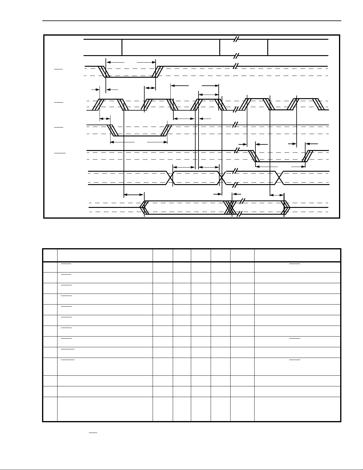
Preliminary Information MT8910-1
F0b
C4b
SFb
F0od
DSTi/
CDSTi
DSTo/
CDSTo
BIT 0, CHANNEL 31
V
OH
V
OL
t
V
OH
V
OL
V
OH
V
OL
V
OH
V
OL
V
IH
V
IL
V
OH
V
OL
t
SFD
CFD
t
FPW
t
DZA
t
SFW
BIT 7, CHANNEL 0
t
CFD
t
t
C4L
SIS
t
P4o
t
t
C4H
C4T
t
SIH
t
DAA
t
DFD
t
DAZ
t
DFW
t
DFD
Figure 17 - ST-BUS Timing NT Mode
AC Electrical Characteristics† - ST-BUS Timing NT Mode (Ref. Figure 17)
Characteristi cs Sym Min Typ‡Max Units Test Conditions
1F0b
2F0b
3C4b
4C4b
5C4b
6C4b
7SFb
8SFb
9F0od
10 F0 od
1 1 Serial Input Setup Time t
12 Serial Input Hold Time t
13 Serial Output Delay Act to Act
† Timing is over recommended temperature & power supply voltages.
‡ Typical figures are at 25°C and are for design aid only: not guaranteed and not subject to producti on testing.
Notes 1) The C4b
Output Pulse Width t
Output Delay t
Output Clock Period t
Pulse Width High t
Pulse Width Low t
Transition Time t
Output Delay t
Output Pulse Width t
Delay t
Pulse Width t
High Z to Act
Act to High Z
2) These timing paramete rs are mode in de pe nd en t (NT or LT).
3) Test ed at 5 .0V, 25°C o nl y.
pulse w id th low will va ry by ±48ns d uri ng a phase-co rr e ct ion c y cl e.
FPW
CFD
P4o
C4H
C4L
C4T
SFD
SFW
DFD
DFW
SIS
SIH
t
DAA
t
DZA
t
DAZ
30 ns CL=150 pF (see Note 2)
50 ns CL=150 pF (see Note 2)
1 cycles CL=150 pF, C4b cycles
60 ns 150 pF (see Note 3)
244 ns 150 pF
88 ns 150 pF
137 ns 150 pF (see Note 1)
15 ns 150 pF
60 ns CL=150 pF (see Note 3)
1 cycles CL=150 pF, C4b cycles
60 ns CL=150 pF (see Notes 2 & 3)
1 cycles CL=150 pF, C4b cy cles (see
Note 2)
120
120
120
ns
ns
ns
150 pF load (see Notes 2 & 3)
150 pF load (see Notes 2 & 3)
150 pF load (see Notes 2 & 3)
9-27
Page 26

MT8910-1 Preliminary Information
NOTE S:
9-28
 Loading...