

Page 1
4-91
Features
• Central office quality DTMF transmitter/receiver
• Low power c onsu mpt ion
• High speed Intel micro interface
• Adjustable guard time
• Automat ic tone bu rst mo de
• Call prog ress ton e det ection t o -30dBm
Applications
• Credit card systems
• Paging systems
• Repeater systems/mobile radio
• Interconn ect di alers
• Persona l comp uters
Description
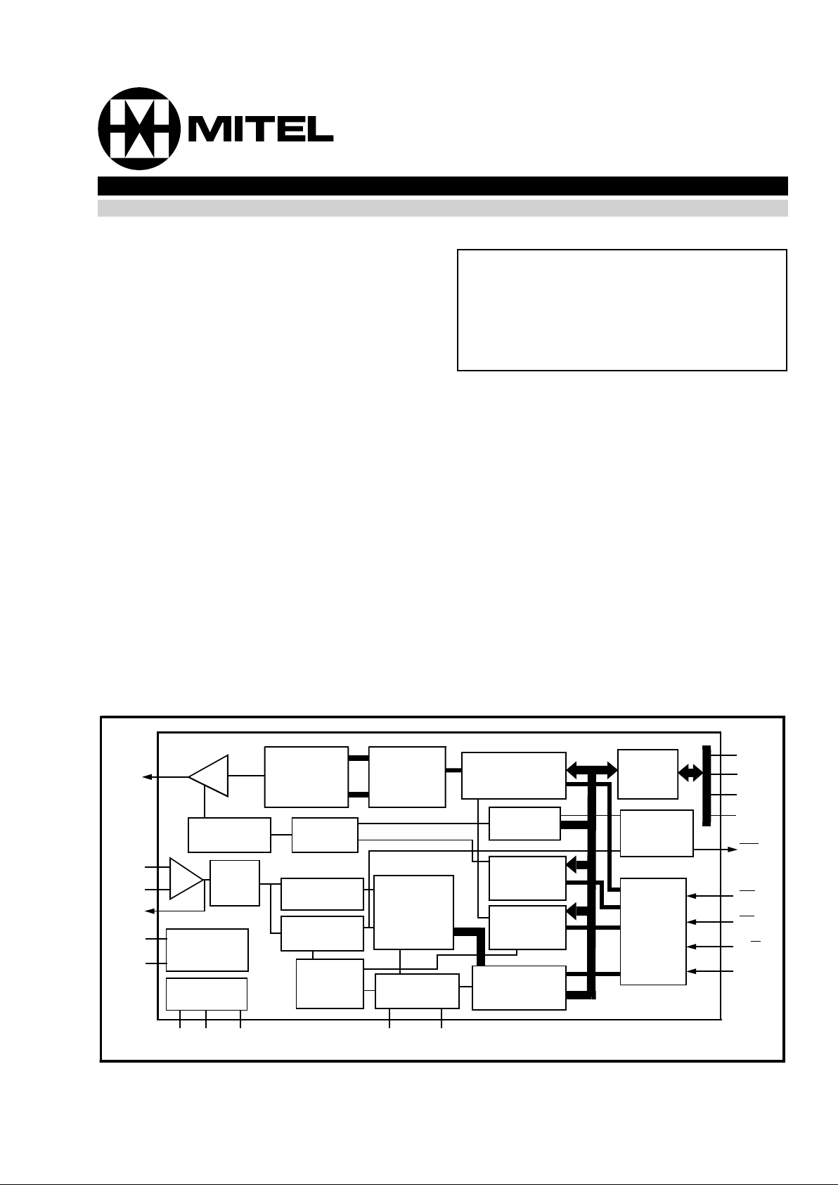
The MT8888C is a monolithic DTMF transceiver with
call progress filter. It is fabricated in CMOS
technology offering low power consumption and high
reliability.
The receiver section is based upon the industry
standard MT8870 DTMF receiver while the
transmitter utilizes a switched capacitor D/A
converter for low distortion, high accuracy DTMF
signalling. Internal counters provide a burst mode
such that tone bursts can be transmitted with precise
timing. A call progress filter can be selected allowing
a microprocessor to analyze ca ll progress tones.
The MT8888C utiliz es an Intel micro int erface, which
allows the device to be connected to a number of
popular microcontrollers with minimal external logic.
The MT8888C-1 is functionally identical to the
MT8888C except the receiver is enhanced to accept
lower level signals, and also has a specified low
signal rejection level.
Ordering Information
MT8888CE/CE-1 20 Pin Plastic DIP
MT8888CC/CC-1 20 Pin Ceramic DIP
MT8888CS/CS-1 20 Pin SOIC
MT8888CN/C N-1 24 Pin SSOP
-40°C to +85°C
Figure 1 - Functional Block Diagram
TONE
IN+
IN-
GS
OSC1
OSC2
V
DDVRefVSS
ESt St/GT
D0
D1
D2
D3
IRQ
/CP
RD
CS
R/W
RS0
∑
D/A
Converters
Row and
Column
Counters
Transmit Data
Register
Data
Bus
Buffer
Tone Burst
Gating Cct.
+
-
Oscillator
Circuit
Bias
Circuit
Control
Logic
Digital
Algorithm
and Code
Converter
Control
Logic
Steering
Logic
Status
Register
Control
Register
A
Control
Register
B
Receive Data
Register
Interrupt
Logic
I/O
Control
Low Group
Filter
High Group
Filter
Dial
Tone
Filter
ISSUE 2 May 1995
MT8888C/MT8888C-1
Integrated DTMFTransceiver
with Intel Micro Interface
Page 2
MT8888C/MT8888C-1
4-92
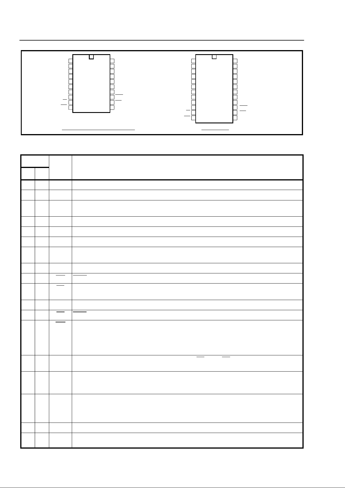
Figure 2 - Pin Connections
Pin Description
Pin #
Name Description
20 24
11 IN+Non-inverting op-amp input.
22 IN-Inverting op-amp input.
33 GSGain Se le c t. Giv es access to output of front end differential amplif ier fo r connection of
feedback resistor.
44V
Ref
Reference Voltage output (VDD/2).
55V
SS
Ground (0V).
66OSC1Oscillator input. This pin can also be driven directly by an external clock.
77OSC2Oscillator output. A 3.579545 MHz crystal conn ected between OSC1 and OSC2 completes
the internal oscillat or circui t. Leave open cir cuit when OSC1 is driven externally.
8 10 TONE Output from inte rnal DTMF transmitte r.
911 WR
Write microprocessor input. TTL compatible.
10 12 CS
Chip Se le c t input . Active Low. This signal must be qualified externally by address latch
enable (ALE) signal, se e Figure 12.
11 13 RS0 Register Select input. Refer to Table 3 for bit inte rp retat ion . TTL compat ibl e.
12 14 RD
Read microprocessor input. TTL compatible.
13 15 IRQ
/CPInterrupt Request/ Cal l Progress (open drain) output . In interrupt mode, this output goes
low when a valid DTMF tone burst has been transmitted or received. In call progress mode,
this pin will output a rectangular signal representative of the input signal appli ed at the input
op-amp. The input signal must be wit hin the bandwidt h limit s of the call progress filter, see
Figure 8.
14-1718-21D0-D3 Microprocessor Data Bus. High impedance when CS
= 1 or RD = 1.
TTL compatib le.
18 22 ES t Early Steering out put. Presen ts a logic high once the digita l algorit hm has det ected a valid
tone pair (signal condition ). Any mome ntary loss of signal condition will cause ES t to return
to a logic low.
19 23 St/GT Steering Input/Guard Time output (bidirectional). A voltage greater than V
TSt
detected at St
causes the device to register the detected tone pair and update the outp ut latch. A voltage
less than V
TSt
frees the device to accept a new tone pair. The GT output acts to reset the
external steering time-const ant; its stat e is a function of ESt and the volt age on St.
20 24 V
DD
Positive power supply (5V typ.).
8,9
16,17
NC No Connection.
1
2
3
4
5
6
7
8
9
10
11
12
20
19
18
17
16
15
14
13
IN+
IN-
GS
VRef
VSS
OSC1
OSC2
TONE
R/W
CS
VDD
St/GT
ESt
D3
D2
D1
D0
IRQ
/CP
RD
RS0
NC
1
2
3
4
5
6
7
8
9
10
11
12
13
14
15
16
24
23
22
21
20
19
18
17
IN+
IN-
GS
VRef
VSS
OSC1
OSC2
NC
TONE
R/W
CS
VDD
St/GT
ESt
D3
D2
D1
D0
NC
NC
IRQ
/CP
RD
RS0
24 PIN SSOP
20 PIN CERDIP/PLASTIC DIP/SOIC
Page 3
MT8888C/MT8888C-1
4-93
Functional Description
The MT8888C/MT8888C-1 Integrated DTMF
Transceiver consists of a high performance DTMF
receiver with an internal gain setting amplifier and a
DTMF generator which employs a burst counter to
synthesize precise tone bursts and pauses. A call
progress mode can be selected so that frequencies
within the specified passband can be detected. The
Intel micro interface allows microcontrollers, such as
the 8080, 80C31/51 and 8085, to access the
MT8888C/MT8888C-1 internal registers.
Input Configuration
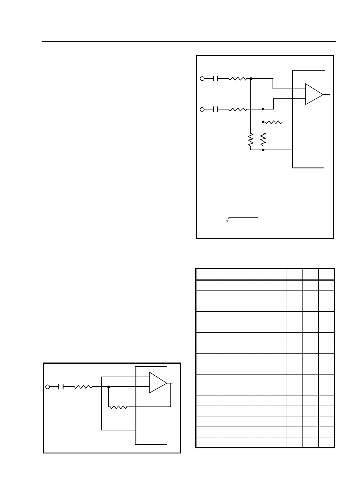
The input arrangement of the MT8888C/MT8888C-1
provides a differential-input operational amplifier as
well as a bias source (V
Ref
), which is used to bias the
inputs at V
DD
/2. Provision is made for connection of
a feedback resistor to the op-amp output (GS) for
gain adjustment. In a single-ended configuration, the
input pins are connected as shown in Figure 3.
Figure 4 shows the necessary connections for a
differential input configuration.
Receiver Se ction
Separation of the low and high group tones is
achieved by applying the DTMF signal to the inputs
of two sixth-order switched capacitor bandpass
filters, the bandwidths of which correspond to the low
and high group frequencies (see Table 1). These
filters incorporate notches at 350 Hz and 440 Hz for
exceptional dial tone rejection. Each filter output is
followed by a single order switched capacitor filter
section, which s mooths the signals prior to limiting.
Limiting is performed by high-gain comparators
which are provided with hysteresis to prevent
detection of unwanted low-level signals. The outputs
of the comparators provide full rail logic swings at
the frequencies of the incoming DTMF signals.
Figure 3 - Single-Ended Input Configuration
C
R
IN
R
F
IN+
IN-
GS
V
Ref
VOLTAGE GAIN
(A
V
) = RF / R
IN
MT8888C/
MT8888C-1
Figure 4 - Differential Input Configura tion
0= LOGIC LOW, 1 = LOGIC HIGH
Table 1. Functional Encode/Decode Table
F
LOW
F
HIGH
DIGIT D
3
D
2
D
1
D
0
697 1209 1 0 0 0 1
697 1336 2 0 0 1 0
697 1477 3 0 0 1 1
770 1209 4 0 1 0 0
770 1336 5 0 1 0 1
770 1477 6 0 1 1 0
852 1209 7 0 1 1 1
852 1336 8 1 0 0 0
852 1477 9 1 0 0 1
941 1336 0 1 0 1 0
941 1209 * 1 0 1 1
941 1477 # 1 1 0 0
697 1633 A 1 1 0 1
770 1633 B 1 1 1 0
852 1633 C 1 1 1 1
941 1633 D 0 0 0 0
C1
C2
R1
R2
R3
R4
R5
IN+
IN-
GS
V
Ref
MT8888C/
DIFFERENTIAL INPUT AMPLIFIER
C1 = C2 = 10 nF
R1 = R4 = R5 = 100 kΩ
R2 = 60kΩ, R3 = 37.5 kΩ
R3 = (R2R5)/(R2 + R5)
VOLTAGE GAIN
(A
V
diff) - R5/R1
INPUT IMPEDANCE
(Z
IN
diff) = 2 R12 + (1/ωC)
2
MT8888C-1
Page 4
MT8888C/MT8888C-1
4-94
Following the filter section is a decoder employing
digital counting techniques to determine the
frequencies of the incoming tones and to verify that
they correspond to standard DTMF frequencies. A
complex averaging algorithm protects against tone
simulation by extraneous signals such as vo ice while
providing tolerance to small frequency deviations
and variations. This averaging algorithm has been
developed to ensure an optimum combination of
immunity to talk-off and tolerance to the presence of
interfering frequencies (third tones) and noise. When
the detector recognizes the presence of two valid
tones (this is referred to as the “signal condition” in
some industry specifications) the “Early Steering”
(ESt) output will go to an active state. Any
subsequent loss of signal condition will cause ESt to
assume an inactiv e state.
Steering Circuit
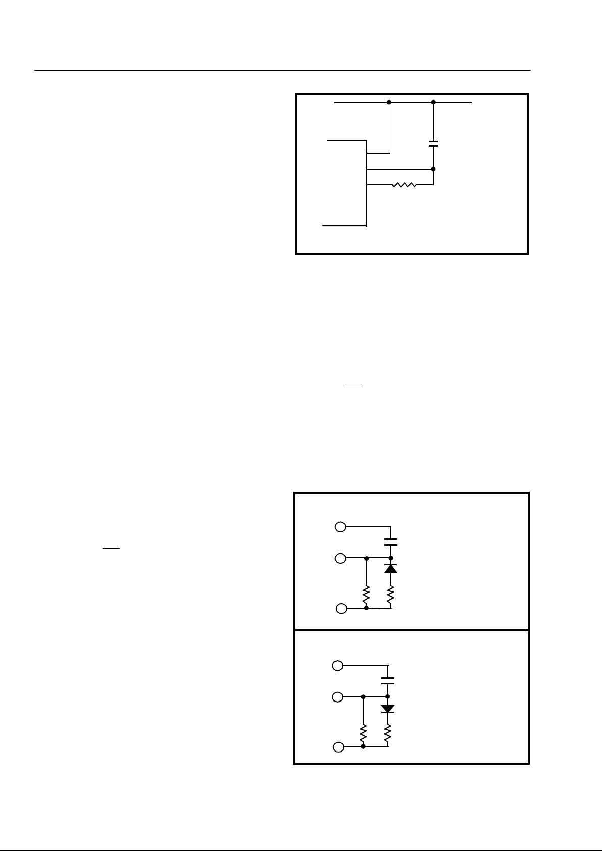
Before registration of a decoded tone pair, the
receiver checks f or a v alid signal duration (referred
to as character recognition condition). This check is
performed by an external RC time constant driven by
ESt. A logic high on ESt causes v
c
(see Figure 5) to
rise as the capacitor discharges. Provided that the
signal condition is maintained (ESt remains high) for
the validation period (t
GTP
), vc reaches the threshold
(V
TSt
) of the steering logic to register the tone pair,
latching its corresponding 4-bit code (see Table 1)
into the Receive D ata Regist er. At this point the GT
output is activated and drives v
c
to VDD. GT
continues to drive high as long as ESt remains high.
Finally, after a short de lay to a ll ow th e o ut put latch to
settle, the delayed steering output flag goes high,
signalling that a received tone pair has been
registered. The status of the delayed steering flag
can be monitored by checking the appropriate bit in
the status register. If Interrupt mode has been
selected, the IRQ
/CP pin will pull low when the
delayed s t e er ing flag is a cti v e.
The contents of the output latch are updated on an
active delayed steering transition. This data is
presented to the four bit bidirectional data bus when
the Receive Data Register is read. The steering
circuit works in reverse to validate the interdigit
pause between signals. Thus, as well as rejecting
signals too short to be considered valid, the receiver
will tolerate signal interruptions (drop out) too short
to be considered a valid pause. This facility, together
with the capability of selecting the steering time
constants externally, allows the designer to tailor
performance to meet a wide variety of system
requirements.
Figure 5 - Basic Steering Circuit
Guard Time Adjustment
The simple steering circuit shown in Figure 5 is
adequate for most applications. Component values
are chosen according to the following inequalities
(see Figure 7):
t
REC
≥ t
DPmax+tGTPmax
- t
DAmin
t
REC
≤ t
DPmin+tGTPmin
- t
DAmax
tID ≥ t
DAmax+tGTAmax
- t
DPmin
tDO ≤ t
DAmin+tGTAmin
- t
DPmax
The value of tDP is a device parameter (see AC
Electrical Characteristics) and t
REC
is the minimum
signal duration to be recognized by the receiver. A
value for C1 of 0.1 µF is recommended for most
Figure 6 - Guard Time Adjustment
V
DD
V
DD
St/GT
ESt
C1
Vc
R1
MT8888C/
t
GTA
= (R1C1) In (VDD / V
TSt
)
t
GTP
= (R1C1) In [VDD / (VDD-V
TSt
)]
MT8888C-1
V
DD
St/GT
ESt
V
DD
St/GT
ESt
C1
R1
R2
C1
R1
R2
t
GTA
= (R1C1) In (VDD/V
TSt
)
t
GTP
= (RPC1) In [VDD / (VDD-V
TSt
)]
R
P
= (R1R2) / (R1 + R2)
t
GTA
= (RpC1) In (VDD/V
TSt
)
t
GTP
= (R1C1) In [VDD / (VDD-V
TSt
)]
R
P
= (R1R2) / (R1 + R2)
a) decreasing tGTP; (tGTP < tGTA)
b) decreasing tGTA; (tGTP > tGTA)
Page 5
MT8888C/MT8888C-1
4-95
applications, leaving R1 to be selected by the
designer. Different steering arrangements may be
used to select independent tone present (t
GTP
) and
tone absent (t
GTA
) guard times. This may be
necessary to meet system specifications which place
both accept and reject limits on tone duration and
interdigital pause. Guard time adjustment also allows
the designer to tailor system parameters such as talk
off and noise imm unity.
Increasing t
REC
improves talk-off performance since
it reduces the probability that tones simulated by
speech will maintain a valid signal condition long
enough to be registered. Alternatively, a relatively
short t
REC
with a long tDO would be appropriate for
extremely noisy environments where fast acquisition
time and immunity to tone drop-outs are required.
Design information for guard time adjustment is
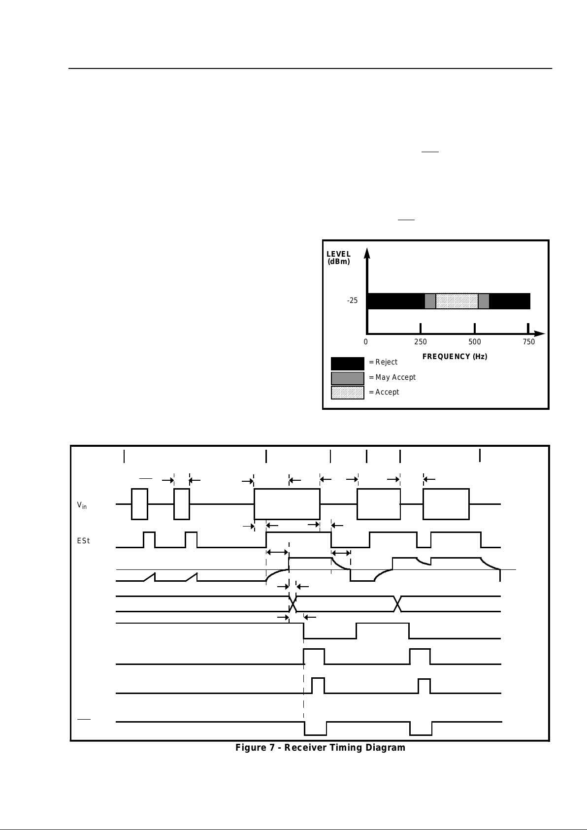
shown in Figure 6. The receiver timing is shown in
Figure 7 with a description of the events in Figure 9.
Call Progress Filter
A call progress mode, using the MT8888C/
MT8888C-1, can be selected allowing the detection
of various tones, which identify the progress of a
telephone call on the network. The call progress
tone input and DTMF input are common, however,
call progress tones can only be detected when CP
mode has been selected. DTMF signals cannot be
detected if CP mode has been selected (see Table
7). Figure 8 indicates the useful detect bandwidt h of
the call progress filter. Frequencies presented to the
input, which are within the ‘accept’ bandwidth limits
of the filter, are hard-limited by a high gain
comparator with the IRQ
/CP pin serving as the
output. The squarewave output obtained from the
schmitt trigger can be analyzed by a microprocessor
or counter arrangement to determine the nature of
the call progress tone being detected. Frequencies
which are in the ‘reject’ area will not be detected and
consequently the IRQ
/CP pin will remain low.
Figure 8 - Call Progress Response
AAA
AAA
AAA
AAA
AAAA
AAAA
AAAA
AAAA
AAAA
AAAA
AAAA
AAAA
A
A
A
A
AAA
AAA
AAA
AAAA
AAAA
AAAA
AAAA
A
A
A
A
A
AA
LEVEL
(dBm)
FREQUENCY (Hz)
-25
0 250 500 750
= Reject
= May Accept
= Accept
Figure 7 - R ece iver Tim ing Diag ram
V
in
ESt
St/GT
RX
0
-RX
3
b3
b2
Read
Status
Register
IRQ
/CP
EVENTS
ABCDEF
t
REC
t
REC
t
ID
t
DO
TONE #n
TONE
#n + 1
TONE
#n + 1
t
DP
t
DA
t
GTP
t
GTA
t
PStRX
t
PStb3
DECODED TONE # (n-1)
# n
# (n + 1)
V
TSt
Page 6

MT8888C/MT8888C-1
4-96
Figur e 9 - D e scri pt ion of Tim in g Ev en ts
EXPLANATION OF EVENTS
A) TONE BURSTS DETECTED, TONE DURATION INVA LID, RX DATA REGISTER NOT UPDATED.
B) TONE #n DETECTED, TONE DURATION VAL ID, TONE DECODED AND LATCHED IN RX DATA REGISTER.
C) END OF TONE #n DETECTED, TONE A BSENT DURATION VALID, INFORMATION IN RX DATA REGISTER
RETAINE D UNTI L NEXT VALID TONE PAIR.
D) TONE #n+1 DETECTED, TONE DURATION VALID, TONE DECODED AND LATCHED IN RX DATA REGISTER.
E) ACCEPTABLE DROPOUT OF TONE #n+1, TONE ABSENT DURATION INVALID, DATA REMAINS UNCHANGED.
F) END OF TONE #n+1 DETECTED, TONE ABSENT DURATION VALID, INFORMATION IN RX DATA RE GISTE R
RETAINE D UNTI L NEXT VALID TONE PAIR.
EXPLANATION OF SYMBOLS
V
in
DTMF COMPOSITE INPUT SIG NA L.
ESt EARLY S TEERING OUTPUT. INDICATES DETECTION OF VALID TONE FREQUENCIES.
St/GT STEERING INPUT/GUARD TIME OUTPUT. DRIVES EXTERNAL RC TIMING CIRCUIT.
RX
0
-RX34-BIT DECODED DATA IN RECEIVE DATA REGISTER
b3 DEL AYED STEERING. INDICATES THAT VALID FREQUENCIES HAVE BEEN PRESENT/ABSENT FOR THE
REQUIRED GUARD TIME THUS CONSTITUTING A VALID SIGNAL. ACTIVE LOW FOR THE DURATION OF A
VALID DTMF SIGNAL.
b2 INDICATES THAT VALID DATA IS IN THE RECEIVE DATA REGISTER. THE BIT IS CLE ARED AFTER THE STATUS
REGISTER IS READ.
IRQ
/CP INTERRUPT IS ACTIVE INDICATING THAT NEW DATA IS IN T HE RX DATA REGI STER. THE INTERRUPT IS
CLEARED AFTER THE STAT US R EGI STER IS READ.
t
REC
MAXIMUM DTMF SIGNAL DURATION NOT DETECTED AS VALID.
t
REC
MINIMUM DTMF SIGNAL DURATION REQUIRED FOR VALID RECOGNITION.
t
ID
MINIMUM TIME BET WEEN VALID SEQUENTIAL D TMF SIG NAL S.
t
DO
MAXIMUM ALLOWABLE DROPOUT DURING VALID DTMF SIGNAL.
t
DP
TIME TO DETECT VALID FREQUENCIES PRESENT.
t
DA
TIME TO DETECT VALID FREQUENCIES ABSENT.
t
GTP
GUARD TIME, TO NE PR ESEN T.
t
GTA
GUARD TIME, TO NE ABSEN T.
DTMF Generator
The DTMF transmitter employed in the MT8888C/
MT8888C-1 is capable of generating all sixteen
standard DTMF tone pairs with low distortion and
high accuracy. All frequencies are derived from an
external 3.579545 MHz crystal. The sinusoidal
waveforms for the individual tones are digitally
synthesized using row and column programmable
dividers and switched capacitor D/A converters. The
row and column tones are mixed and filtered
providing a DTMF signal with low total harmonic
distortion and high accuracy. To specify a DTMF
signal, data conforming to the encoding format
shown in Table 1 must be written t o the transmit Data
Register. Note that this is the same as the receiver
output code. The individual tones which are
generated (f
LOW
and f
HIGH
) are referred to as Low
Group and High Group tones. As seen from the
table, the low group frequencies are 697, 770, 852
and 941 Hz. The high group frequencies are 1209,
1336, 1477 and 1633 Hz. Typically, the high group to
low group amplitude ratio (twist) is 2 dB to compensate for high group attenuation on long loops.
The period of each tone consists of 32 equal time
segments. The period of a tone is controlled by
varying the length of these time segments. During
write operations to the Transm it Data Register the 4
bit data on the bus is latched and converted to 2 of 8
coding for use by the programmable divider circuitry.
This code is used to specify a time segment length,
which will ultimately determine the frequency of the
tone. When the divider reaches the appropriate
count, as det ermined by the input code, a reset pulse
is issued and the counter starts again. The number
of time segm ents is fixed at 32, however, by varying
the segment length as described above the
frequency can also be varied. The divider output
clocks another counter, which addresses the
sinewave lookup ROM.
The lookup table contains codes which are used by
the switched capacitor D/A converter to obtain
discrete and highly accurate DC voltage levels. Two
identical circuits are employed to produce row and
column tones, which are then mixed using a low
noise summing amplifier. The oscillator described
needs no “start-up” time as in other DTMF
generators since the crystal oscillator is running
continuously thus providing a high degree of tone
burst accuracy. A bandwidth limiting filter is
incorporated and serves to attenuate distortion
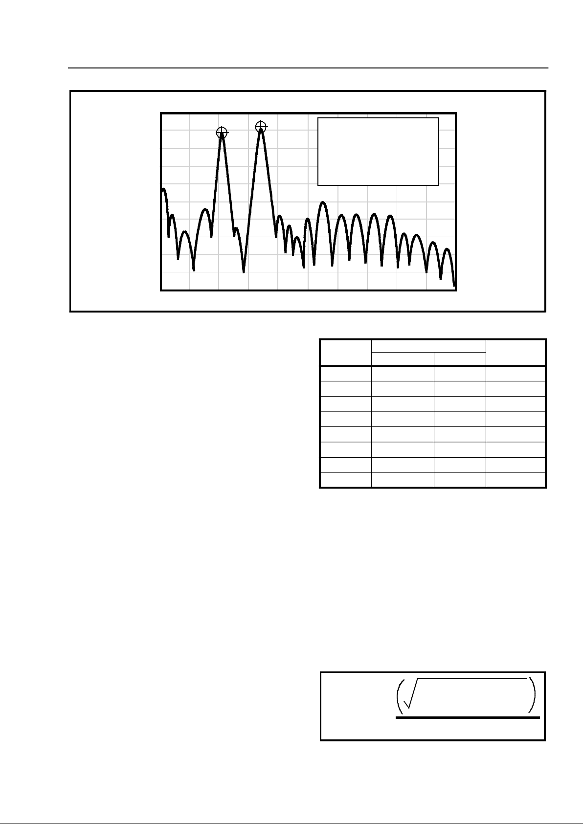
products above 8 kHz. It can be seen from Figure 8
that the distortion products are very low in amplitude.
Page 7
MT8888C/MT8888C-1
4-97
Figure 10 - Spectrum Plot
Scaling Information
10 dB/Div
Start Frequency = 0 Hz
Stop Frequency = 3400 Hz
Marker Frequency = 697 Hz and
1209 Hz
Burst Mode
In certain telephony applications it is required that
DTMF signals being generated are of a specific
duration determined either by the particular
application or by any one of the exchange transmitter
specifications currently existing. Standard DTMF
signal timing can be accom plished by making use of
the Burst M o de. T h e tr an s m itte r is capable o f issu i n g
symmetric bursts/pauses of predeterm ined duration.
This burst/pause duration is 51 ms±1 ms, which is a
standard interval for autodialer and central office
applications. After the burst /pause has been issued,
the appropriate bit is set in the Status Register
indicating that th e transmitter is ready for more data.
The timing described above is available when DTMF
mode has been selected. However, when CP mode
(Call Progress mode) is selected, the burst/pause
duration i s do ub le d to 1 0 2 ms ± 2 ms . No te th a t wh e n
CP mode and Burst mode have been selected,
DTMF tones may be transmitted only and
not
received. In applications where a non-standard
burst/pause time is desirable, a software timing loop
or external timer can be used to provide the timing
pulses when the burst mode is disabled by enabling
and disabling the transmitter.
Single Tone Generation
A single tone mode is available whereby individual
tones from the low group or high group can be
generated. This mode can be used for DTMF test
equipment applications, acknowledgment tone
generation and distortion measurements. Refer to
Control Register B description for details.
Table 2. Actual Frequencies Versus Standard
Requirem ents
Distortion Calculations
The MT8888C/MT8888C-1 is capable of producing
precise tone bursts with minimal error in frequency
(see Table 2). The internal summing amplifier is
followed by a first-order lowpass switched capacitor
filter to minimize harmonic components and
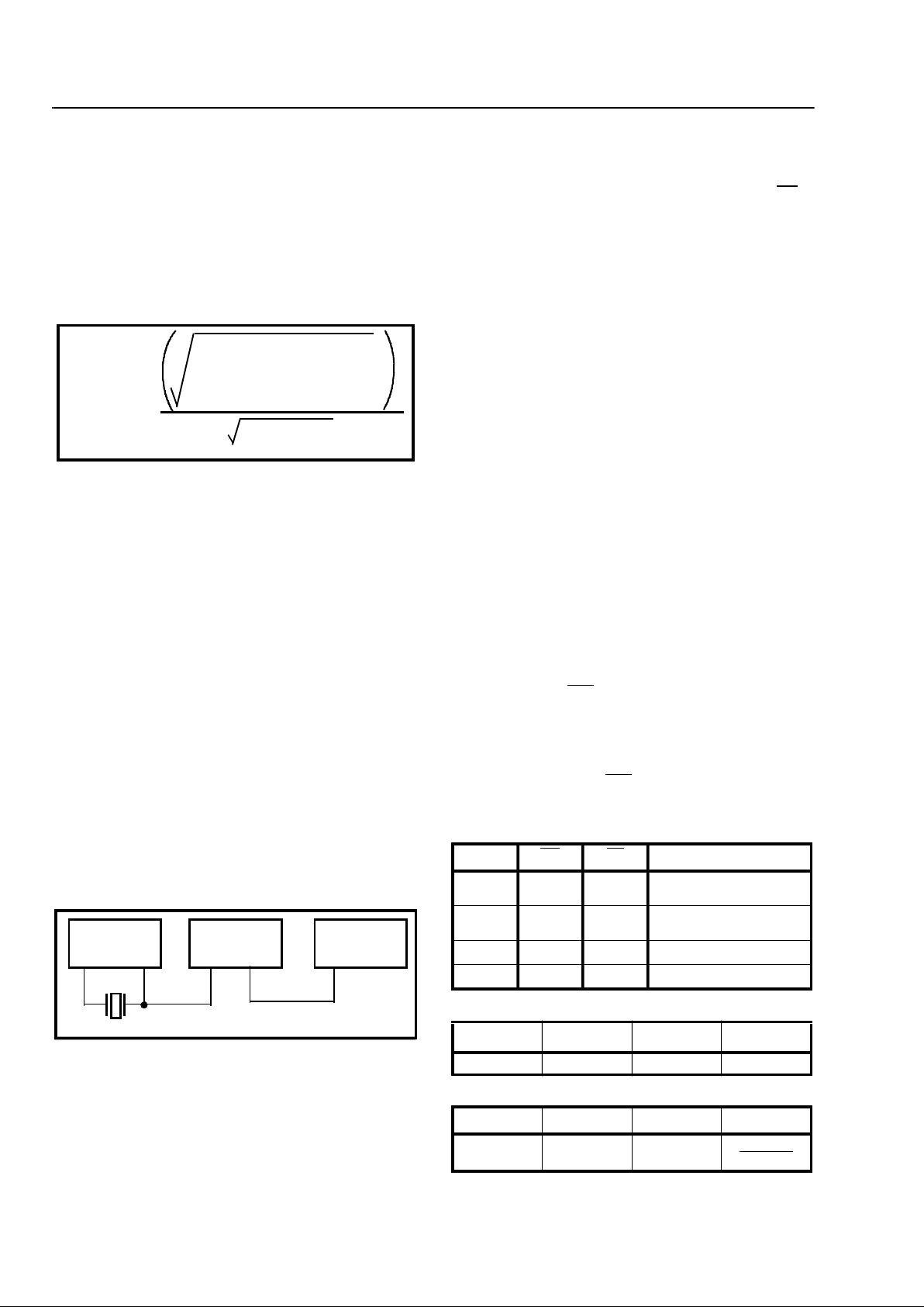
intermodulation products. The total harmonic
distortion for a
single tone
can be calculated using
Equation 1, which is the ratio of the total power of all
the extraneous frequencies to the power of the
fundamental frequency expressed as a percentage.
Equation 1 . THD (%) For a Single Tone
ACTIVE
INPUT
OUTPUT FREQUENCY (Hz)
%ERROR
SPECIFIED ACTUAL
L1
697 699.1 +0.30
L2
770 766.2 -0.49
L3
852 847.4 -0.54
L4
941 948.0 +0.74
H1
1209 1215.9 +0.57
H2
1336 1331.7 -0.32
H3
1477 1471.9 -0.35
H4
1633 1645.0 +0.73
THD (%) = 100
V
fundamental
V
2
2f
+ V
2
3f
+ V
2
4f
+ .... V
2
nf
Page 8
MT8888C/MT8888C-1
4-98
The Fourier components of the tone output
correspond to V
2f
.... Vnf as measured on t he output
waveform. The total harmonic distortion for a
dual
tone
can be calculated using Equation 2. V
L
and V
H
correspond to the low group amplitude and high
group amplitude, respectively and V
2
IMD
is the sum
of all the intermodulation components. The internal
switched-capacitor filter following the D/A converter
keeps distort ion products down to a very low level as
shown in Figure 10.
Equation 2. THD (% ) For a Dual Tone
DTMF Clo ck Ci rcuit
The internal clock circuit is completed with the
addition of a standard television colour burst crystal.
The crystal specification is as follows:
Frequency: 3.579545 MH z
Frequency Tolerance:
±0.1%
Resonance Mode: Parallel
Load Capacitance: 18pF
Maximum Series Resistance: 150 ohms
Maximum Drive Level: 2mW
e.g. CTS K n i g hts M P036S
Toyocom T QC-203-A-9S
A number of MT8888C/MT8888C-1 devices can be
connected as shown in Figure 11 such that only one
crystal is required. Alternatively, the OSC1 inputs on
all devices can be driven fr om a TTL buffer with the
OSC2 outputs left unconnected.
Figure 11 - Common Crystal Connection
Microprocessor Int erf ace
The MT8888C/MT8888C-1 incorporates an Intel
microprocessor interface which is compatible with
fast versions (16 MHz) of the 80C51. No wait cycles
need to be insert ed.
V
2
L
+ V
2
H
V
2
2L
+ V
2
3L
+ .... V
2
nL
+ V
2
2H
+
V
2
3H
+ .. V
2
nH
+ V
2
IMD
THD (%) = 100
MT8888C/
OSC1 OSC2
MT8888C/
OSC1 OSC2
MT8888C/
OSC1 OSC2
3.579545 MHz
MT8888C-1 MT8888C-1 MT8888C-1
Figures 17 and 18 are the timing diagrams for the
Intel 8031, 8051 and 8085 (5 MHz) microcontrollers.
By NAN Ding the add ress latch ena ble (ALE) ou tput
with the high-byte address (P2) decode output, CS
is
generated. Figure 12 summarizes the connection of
these Intel processors to the MT8888C/ MT8888C-1
transceiver.
The microprocessor interface provides access to five
internal registers. The read-only Receive Data
Register contains the decoded output of the last
valid DTMF digit received. Data entered into the
write-only Transmit Data Register will determine
which tone pair is to be generated (see Table 1 for
coding details). Tr ansceiver control is accomplished
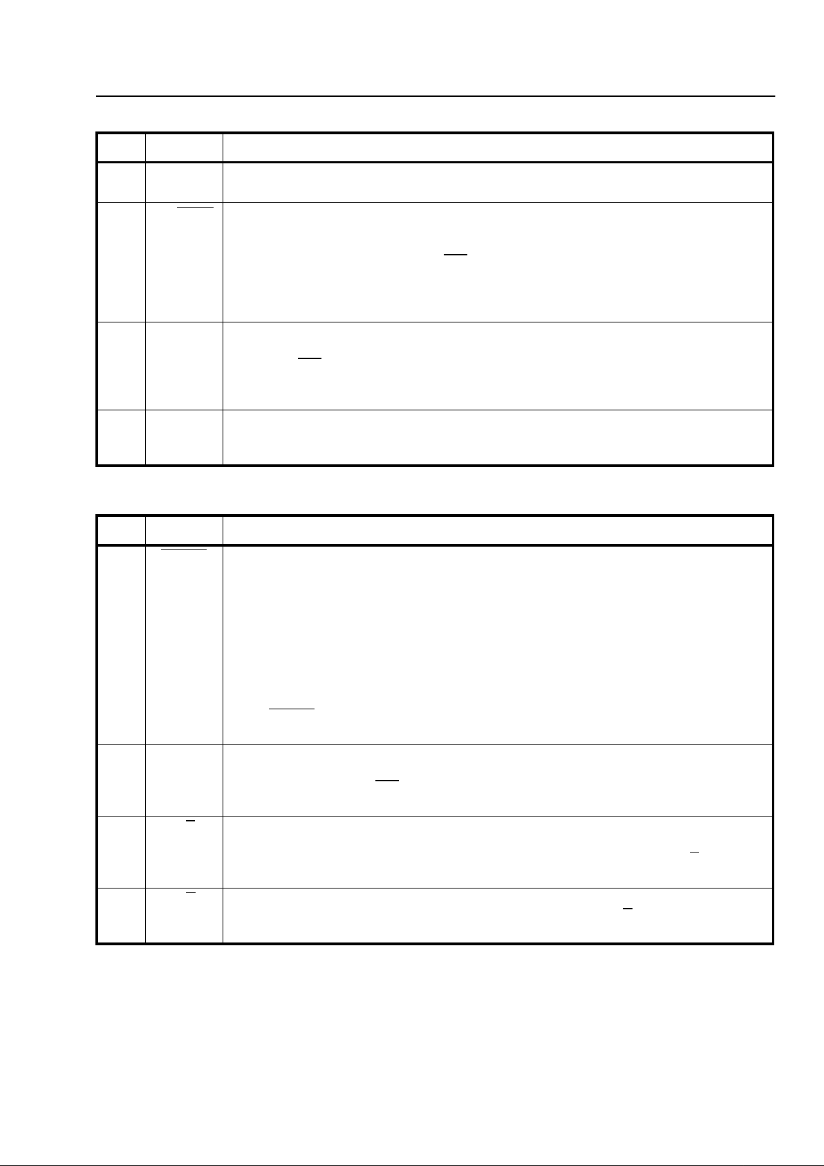
with two control registers (see Tables 6 and 7), CRA
and CRB, which have the same address. A write
operation to CRB is executed by first setting the
most significant bit (b3) in CRA. The following write
operation to the same address will then be direct ed
to CRB, and subsequent writ e cycles will be directed
back to CRA. The read-only status register indicates
the curre n t tr a n sce iver state ( see Table 8).
A software reset must be included at the beginning
of all programs to init ialize the control registers upon
power-up or power reset (see Figure 17). Refer to
Tables 4-7 for bit descriptions of the two control
registers.
The multiplexed IRQ
/CP pin can be programmed to
generate an interrupt upon validation of DTMF
signals or when the transmitter is ready for more
data (burst mode only). Alternat ively, this pin can be
configured to provide a squarewave output of the call
progress signal. The IRQ
/CP pin is an open drain
output and requires an external pull-up resistor (see
Figure 13).
Table 3. Internal Register Functions
Tabl e 4. CRA Bit Po sitions
Tabl e 5. CRB Bit Po sitions
RS0 WR RD FUNCTION
001
Write to Transmit
Data Register
010
Read from Receive
Data Register
101
Write to Control Register
110
Read from Status Register
b3 b2 b1 b0
RSEL IRQ CP/DTMF TOUT
b3 b2 b1 b0
C/R
S/D TEST BURST
ENABLE
Page 9
MT8888C/MT8888C-1
4-99
Table 6. Control Register A Desc ription
Ta ble 7
. Contr ol Register B Des cription
BIT NAME DESCRIPTION
b0 TOUT Tone O utp ut Cont rol. A logic high enables the tone output; a logic low turns the tone output
off. This bit controls all transmit tone functions.
b1 CP/DTM F
Call Progress or DTM F Mode Sel ect. A logic h igh en ables t he receive call progress mode;
a logic low enables DTMF mode. In DTMF mode the device is capable of receiving and
transmitting DTMF sign als. In CP mode a rect angular wave re presentati on of the re ceived
tone signal will be present on the IRQ
/CP output pin if IRQ has been enabled (control
register A, b2=1). In order to be detected, CP signals must be within the bandwidth
specified in the AC Electrical Characteristi cs for Call Progress.
Note: DTMF signals cannot be detected when CP mode is selected.
b2 IRQ Interrupt En able. A logic high enables the interrupt function; a logic low de-activates the
interrupt function. When IRQ is enabled and DTMF mode is selected (control register A,
b1=0), the IRQ
/CP output pin wil l go low when either 1) a va lid DTMF signal has been
received for a valid guard time duration, or 2) the transm itter is ready for more data (burst
mode only).
b3 RSEL Register Select . A logic high selects control register B for the next write cycle to the control
register address. After writing to control regist er B, the following con trol regi ster write cycle
will be directed to control register A.
BIT NAME DES CR I P TION
b0 BURST
Burst Mode Select. A logic hi gh de-activat es burst mode; a l ogic low enables burst m ode.
When activated, the d igital code representing a DTMF sig nal (see Table 1) can be written
to the transmit register, which will re sult in a transmit DTMF tone burst and pause of e qual
durations (typically 51 msec.). Following the pause, the status register will be updated (b1 Transmit Data Register Empty), and an inte rrupt will occur if the interrupt mode has been
enabled.
When CP mode (control register A, b1) is enabled the normal tone burst and pause
durations are extended from a typical duratio n of 51 msec to 102 msec.
When BURST
is high (de-activated) the transmit tone burst duratio n is determined by the
TOUT bit (control register A, b0).
b1 TEST Test Mode Cont rol. A logic high enables the test mode; a logic low de-activate s the test
mode. When TEST is e nabled and DT MF mode is selected (control regi ster A, b1=0), the
signal present on the IRQ
/CP pin will be analogous to the state of the DELAYED
STEERING bit of the status register (see Figure 7, signal b3).
b2 S /D
Single or Dual Tone Generation. A logic high selects the single tone output; a logic low
selects the dual tone (DT MF) output. T he single tone generati on function requires furt her
selection of either the r ow or colum n tones (l ow or hi gh group ) throu gh the C/ R
bit (control
register B, b3).
b3 C/R
Column or Row Tone S ele ct. A logic hi gh select s a column t one o utput; a lo gic low sel ects
a row tone output. This function is used in conjunction with the S/D
bit (control reg ister B,
b2).
Page 10
MT8888C/MT8888C-1
4-100
Ta ble 8. Status Register Description
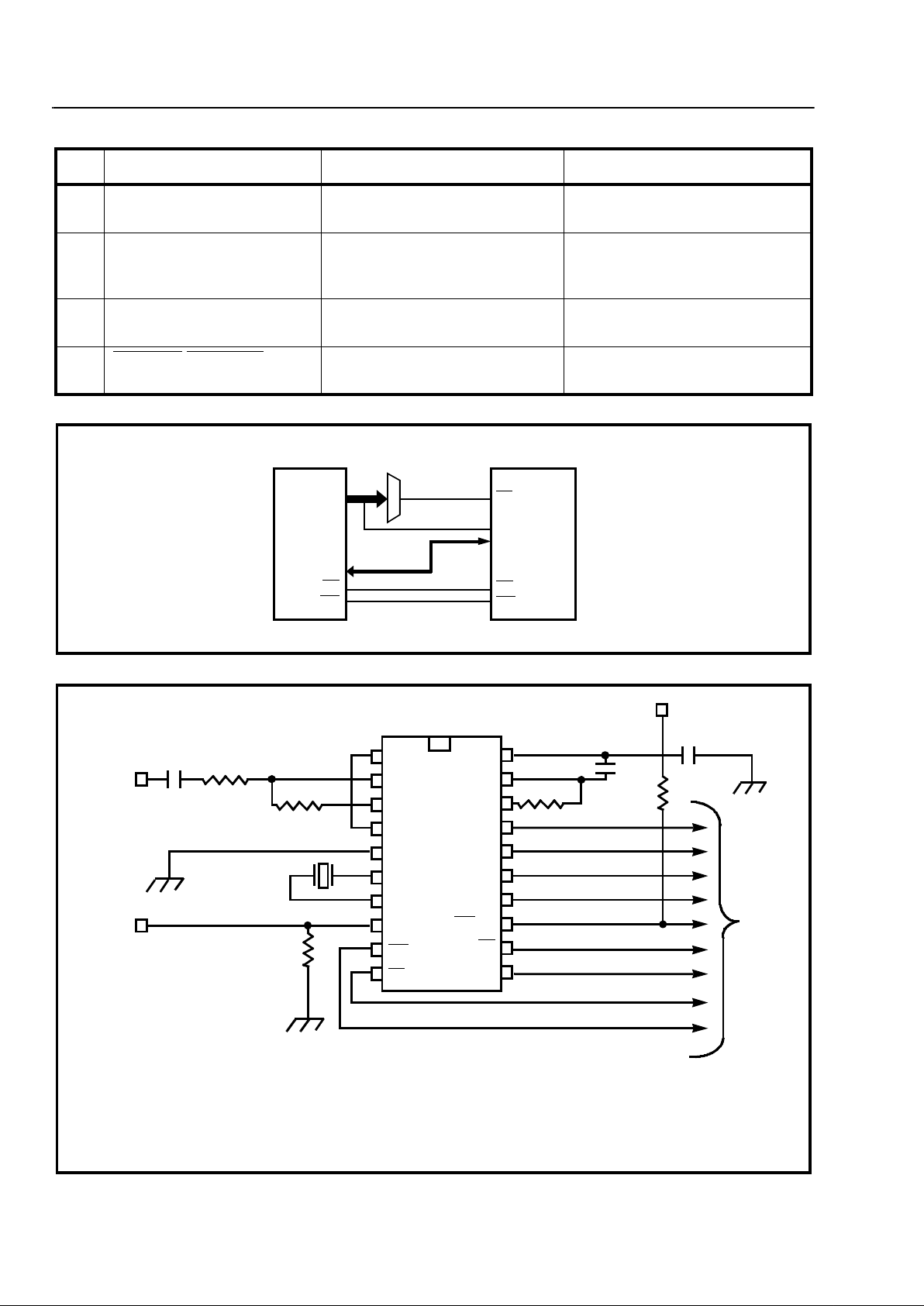
Figure 12 - MT8888C Interface Connections for Various Intel Micros
Figure 1 3 - Application Circuit (Single-Ended Input)
BIT NAME STAT US FL AG SET STATUS FLAG CLEARED
b0 IRQ Interrupt has occurred. Bit one
(b1) or bit two (b2) is set.
Interrupt is inactive. Cleared aft er
Status Register is read.
b1 TRANSMI T DATA
REGISTER EMPTY
(BURST MODE ONLY)
Pause duration has terminat ed
and transmitter is ready for new
data.
Cleared after Stat us Registe r is
read or when in non-burst mode.
b2 RECEIVE DATA REGISTER
FULL
Valid data is in t he Receive Data
Register.
Cleared after Stat us Registe r is
read.
b3 DELAYED
STEERIN G S et upon the valid detect ion of
the absence of a DTMF signal.
Cleared upon the detection of a
valid DTMF signal.
8031/8051
8080/8085
MT8888C/MT8888C-1
A8-A15
PO
RD
WR
CS
RD
WR
RS0
D0-D3
A8
IN+
INGS
VRef
VSS
OSC1
OSC2
TONE
WR
CS
VDD
St/GT
ESt
D3
D2
D1
D0
IRQ
/CP
RD
RS0
DTMF/CP
INPUT
DTMF
OUTPUT
C1
R1
R2
X-tal
R
L
V
DD
C3
C2
R4
R3
To µP
or µC
Notes:
R1, R2 = 100 kΩ 1%
R3 = 374 Ω 1%
R4 = 3.3 kΩ 10%
RL = 10 k Ω (min.)
C1 = 100 nF 5%
C2 = 100 nF 5%
C3 = 100 nF 10%*
X-tal = 3.579545 MHz
* Microprocessor based systems can inject undesirab le noise into th e supply rails.
The performa nce of the MT8 888C /M T88 88C-1 can be optim ized by keepin g
noise on the supply rails to a minimum. The decoupling capacitor (C3) should be
connected close to the device and ground loops should be avoided.
MT8888C/MT8888C-1
Page 11
MT8888C/MT8888C-1
4-101
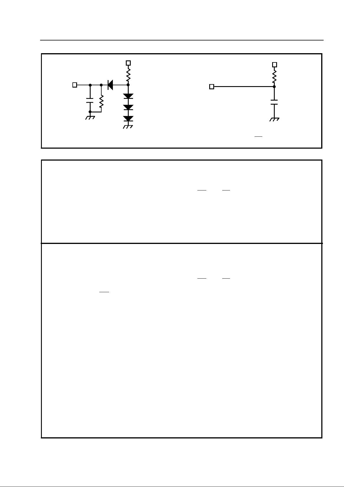
Figure 14 - Test Circuits
Figure 15 - Application Notes
TEST POINT
MMD6150 (or
equivalent)
5.0 VDC
2.4 kΩ
24 kΩ
130 pF
MMD7000 (or
equivalent)
TEST POINT
5.0 VDC
3 kΩ
100 pF
Test load for IRQ
/CP pinTest load for D0-D3 pins
INITIALIZATION PROCEDURE
A software reset must be included at the beginning of all programs to initialize the control registers after
power up.The initialization procedure should be implemented 100ms after power up.
Description: Control Data
RS0 WR
RD b3 b2 b1 b0
1) Read Status Register 1 1 0 X X X X
2) Write to Control Regist er 1 0 1 0 0 0 0
3) Write to Control Regist er 1 0 1 0 0 0 0
4) Write to Control Regist er 1 0 1 1 0 0 0
5) Write to Control Regist er 1 0 1 0 0 0 0
6) Read Status Register 1 1 0 X X X X
TYPICAL CONTROL SEQUENCE FOR BURST MODE APPLICATIONS
Transmit DTMF tones of 50 ms burst/50 ms pause and Receive DTMF Tones.
Sequence:
RS0 WR
RD b3 b2 b1 b0
1) Write to Control Regist er A 1 0 1 1 1 0 1
(tone out, DTM F, IRQ
, Select Control Regist er B)
2) Write to Control Regist er B 1 0 1 0 0 0 0
(burst mode)
3) Write to Transmit Data Register 0 0 1 0 1 1 1
(send a digit 7)
4) Wait for an interrupt or poll Status Register
5) Read the Status Register 1 1 0 X X X X
-if bit 1 is set, the Tx is ready for the next tone, in which case...
Write to Transmit Register 0 0 1 0 1 0 1
(send a digit 5)
-if bit 2 i s se t, a D T MF tone has been r ec e ive d, i n wh ich case....
Read th e Re cei v e Da ta R e gis te r 0 1 0 X X X X
-if both b its a r e set...
Read th e Re cei v e Da ta R e gis te r 0 1 0 X X X X
Write to Transmit D a ta R e gis te r 0 0 1 0 1 0 1
NOTE: IN THE TX BURST MODE, STATUS REGISTER BIT 1 WILL NOT BE SET UNTIL 100 ms (±2 ms) AFTER THE DATA IS
WRITTEN TO THE TX DATA REGISTER. IN EXTENDED BURST M ODE THIS TIME WILL BE DOUBLED TO 200 ms ( ± 4 ms)
.
Page 12
MT8888C/MT8888C-1
4-102
* Excee di ng these values may cause pe rm anen t damage . Function al ope rati on under the se conditi ons is not implie d.
‡ Typical figures are at 25 °C and for design aid only: not guara ntee d and not sub ject to productio n testi ng .
† Characteristics are over recommended operating conditions unless otherwise stated.
‡ Typical figures are at 25 °C, V
DD
=5V and for design aid only: not guaranteed and not subject to production testing.
* Se e “Not es” followi ng AC Electrical Chara cteri st ics Tables.
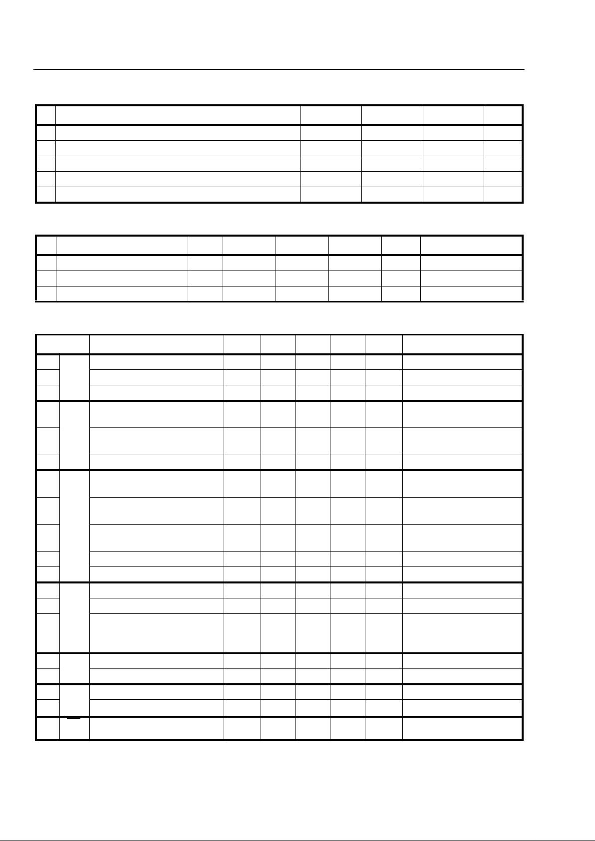
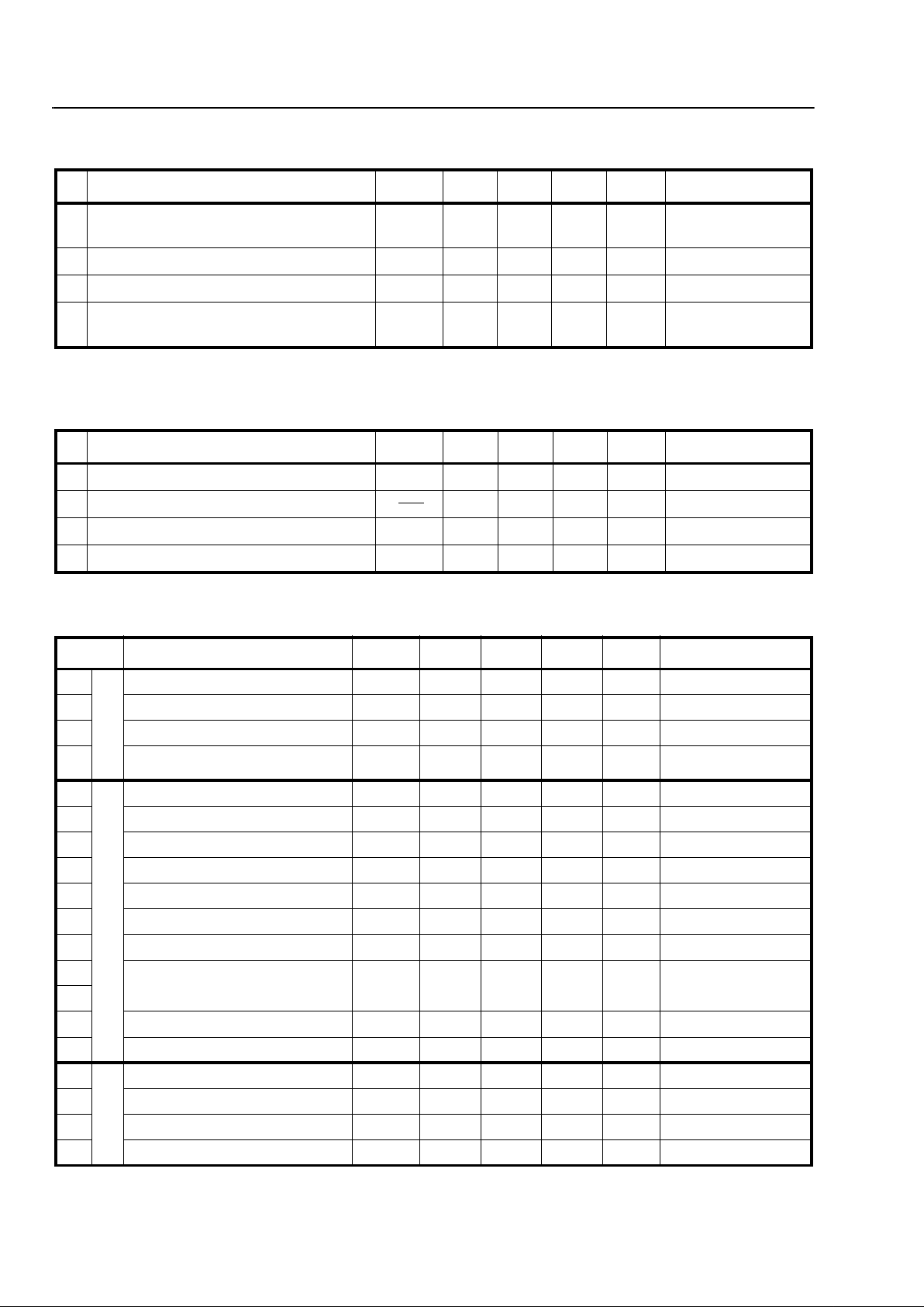
Absolute Maximum Ratings*
Parameter Symbol Min Max Units
1 Power supply voltage V
DD-VSS
V
DD
6V
2 Voltage on any pin V
I
VSS-0.3 VDD+0.3 V
3 Current at any pin (Except V
DD and VSS
)10mA
4 Storage temperature T
ST
-65 + 150 °C
5 Package power dissipation P
D
1000 mW
Recommended Operating Con ditions - Voltages are with respect to ground (V
SS
) unless otherwise stated.
Parameter Sym Min Typ
‡
Max Units Test Conditions
1 Positive power supply V
DD
4.75 5.00 5.25 V
2 Operating temperature T
O
-40 +85 °C
3 Crystal clock frequen cy f
CLK
3.575965 3.579545 3.583124 MHz
DC Electrical Characteristics
†
- VSS=0 V.
Characteris tics Sym Min Typ‡Max Units Test Conditions
1
S
U
P
Operating supply voltage V
DD
4.75 5.0 5.25 V
2 Operating supply current I
DD
7.0 11 mA
3 Power consumption P
C
57.8 mW
4
I
N
P
U
T
S
High level input voltage
(OSC1)
V
IHO
3.5 V N ot e 9*
5 Low level input voltage
(OSC1)
V
ILO
1.5 V No t e 9*
6 Steering threshold voltag e V
TSt
2.2 2.3 2.5 V VDD=5V
7
O
U
T
P
U
T
S
Low level output voltag e
(OSC2) V
OLO
0.1 V
No load
Note 9*
8 High level output voltage
(OSC2) V
OHO
4.9 V
No load
Note 9*
9 Output leakage current
(IRQ) I
OZ
110µAVOH=2.4 V
10 V
Ref
output voltage V
Ref
2.4 2.5 2.6 V No load, VDD=5V
11 V
Ref
output resistance R
OR
1.3 kΩ
12
D
i
g
i
t
a
l
Low level input voltage V
IL
0.8 V
13 High level input voltage V
IH
2.0 V
14 Input leakage current I
IZ
10 µAVIN=VSS to V
DD
15
Data
Bus
Source current I
OH
-1.4 -6.6 mA VOH=2.4V
16 Sink current I
OL
2.0 4.0 mA VOL=0.4V
17
ESt
and
St/Gt
Source current I
OH
-0.5 -3.0 mA VOH=4.6V
18 Sink current I
OL
24 mAVOL=0.4V
19
IRQ/
CP
Sink current I
OL
416 mAVOL=0.4V
Page 13
MT8888C/MT8888C-1
4-103
‡ Typical figures are at 25°C and for design aid only: not guarant ee d and not subject to product io n testing .
† Characteristics are over recommended temperature and at V
DD
=5V, using the test circuit shown in Figure 13.
† Characteristics are over recommended operating conditions (unless otherwise stated)
using the test circuit shown in Figure 13.
† Characteristics are over recommended operating conditions unless otherwise stated.
‡ Typical figures are at 25°C, VDD = 5V, and for design aid only: not guaranteed and not subject to production testing.
* *Se e “Not es” foll owi ng AC Electrical Characterist ic s Tables.
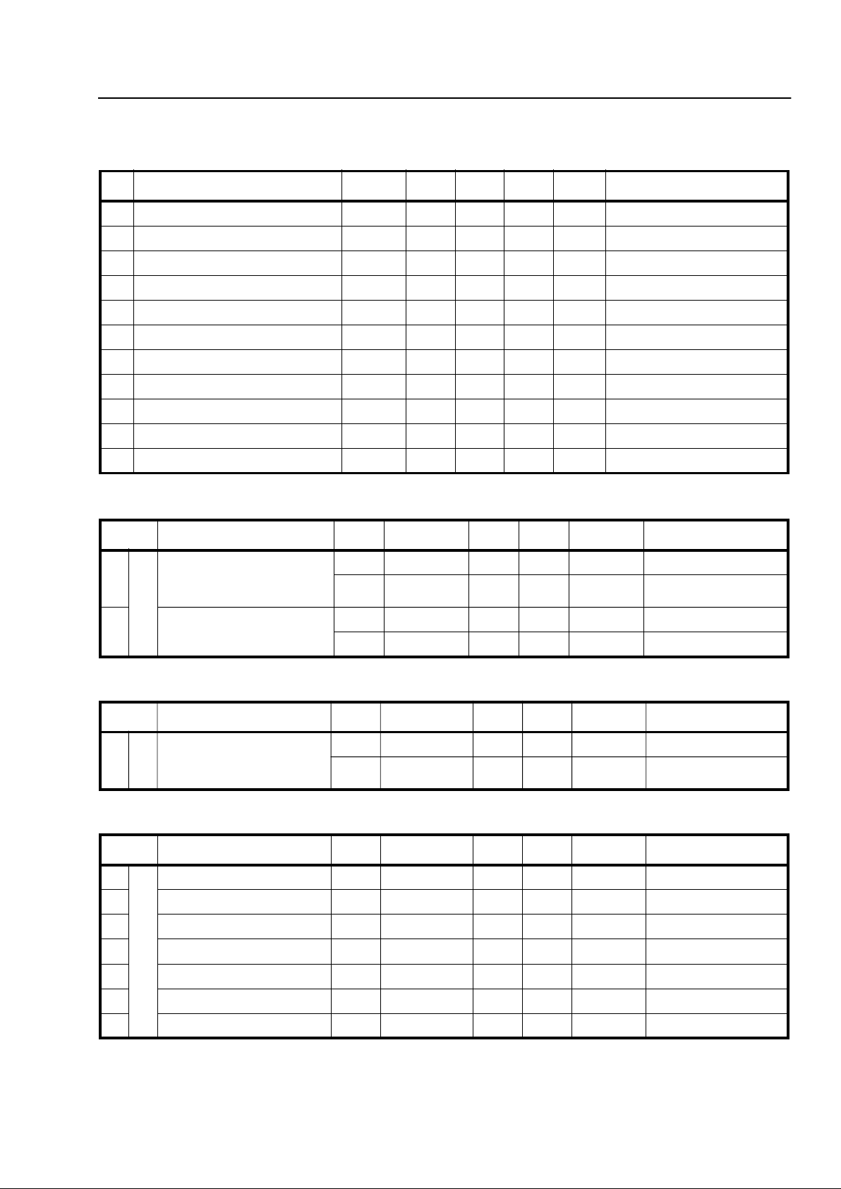
Electrical Characteristics
Gain Setting Am plifier - Voltages are with respect to ground (V
SS
) unless otherwise stated, VSS= 0V, VDD=5V, TO=25°C.
Characteristics Sym Min Typ‡Max Units Test Conditions
1 Input leakage current I
IN
±100 nA VSS ≤ VIN ≤ V
DD
2 Input resistan ce R
IN
10 MΩ
3 Input offset volta ge V
OS
25 mV
4 Power supply rejection PSRR 60 dB 1 kHz
5 Common mo de rejecti on CMRR 60 dB 0.75 ≤ V
IN
≤ 4.25V
6 DC open loop voltage gain A
VOL
65 dB
7 Unity gain ban dwidt h BW 1.5 MHz
8 Output voltage swing V
O
4.5 V
pp
RL ≥ 100 kΩ to V
SS
9 Allowable capacitive load (GS) C
L
100 pF
10 Allowable resistive load (GS) R
L
50 kΩ
11 Common mode range V
CM
3.0 V
pp
No Load
MT8888C-1 AC Electrical Characteristics† - Voltages are with respect to ground (V
SS
) unless otherwise stated.
Characteristics Sym Min Typ Max Units Notes*
1
R
X
Val id input signal levels
(each tone of composite
signal)
-31 +1 dBm 1,2,3,5 ,6
21.8 869 mV
RMS
1,2,3,5 ,6
2 Input Signal Level Reject -37 dBm 1,2, 3,5,6
10.9 mV
RMS
1,2,3,5 ,6
MT8888C AC Electrical Characteristics
†
- Volt ag es are with respect to groun d (V
SS
) unless otherwise stated.
Characteristics Sym Min Typ‡Max Units Notes*
1
R
X
Valid input signal levels
(each tone of composite
signal)
-29 +1 dBm 1,2,3,5,6
27.5 869 mV
RMS
1,2,3,5,6
AC Electrical Characteristics† - Voltages are with respect to ground (V
SS
) unless otherwise stated. fC=3.579545 MHz
Characteristics Sym Min Typ‡Max Units Notes*
1
R
X
Positive twist accept 8 dB 2,3,6,9
2 Negative twist accept 8 dB 2,3,6,9
3 Freq. deviati on a ccep t ±1.5%± 2Hz 2,3,5
4 Freq. deviation reject ±3.5% 2,3,5
5 Third tone tolerance -16 dB 2,3,4, 5,9 ,10
6 Noise tolerance -12 dB 2,3,4,5,7,9,10
7 Dial to ne tolera n ce 22 dB 2 ,3, 4, 5,8 ,9
Page 14
MT8888C/MT8888C-1
4-104
† Characteristics are over recommended operating conditions unless otherwise stated
‡ Typical figures are at 25°C, V
DD
=5V, a nd for design ai d only: not guarant eed and not subject to produ ctio n testing
† Characteristics are over recommended operating conditions unless otherwise stated
‡ Typical figures are at 25°C, V
DD
=5V, a nd for design ai d only: not guarant eed and not subject to produ ctio n testing
† Timing is over recommended temperature & power supply voltages.
‡ Typical figures are at 25°C and for design aid only: not guarantee d and not subject to product ion testi ng.
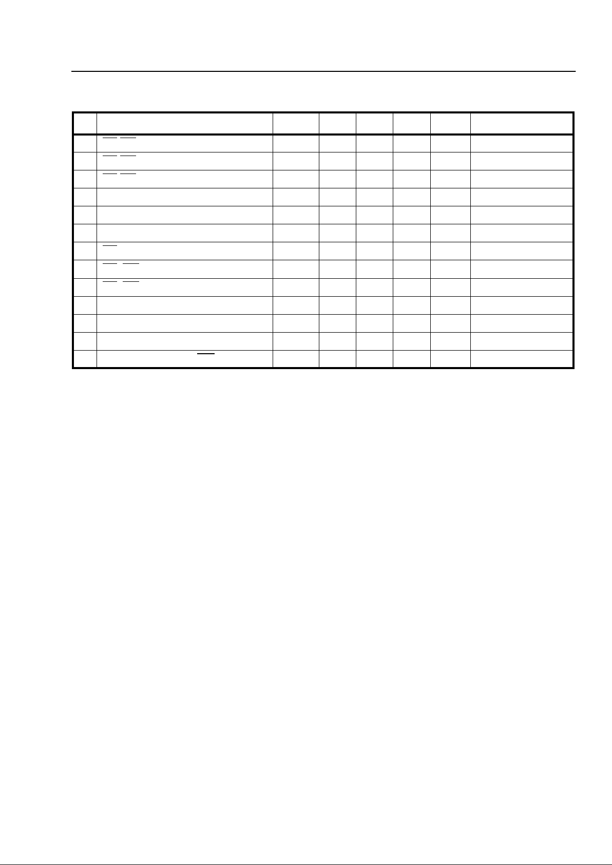
AC Electrical Characteristics†- Call Progress - V oltages are with respect to ground (V
SS
), unless otherwise stated .
Characteristics Sym Min Typ‡Max Units Condition s
1 Accept Bandwidth f
A
310 500 Hz @ -25 dBm,
Note 9
2 Lower freq. (REJECT) f
LR
290 Hz @ -25 dBm
3 Upper freq. (REJECT) f
HR
540 Hz @ -25 dBm
4 Call progress tone detect level (total
power)
-30 dBm
AC Electrical Characteristics†- DTMF Reception - Typical DTMF tone accept and reject requirements. Act ual
values are user selectable as per Figures 5, 6 and 7.
Characteristics Sym Mi n Typ
‡
Max Units Conditions
1 Minimum tone accept durati on t
REC
40 ms
2 Maximum tone reject duration t
REC
20 ms
3 Minimum interdigit pause durati on t
ID
40 ms
4 Maximum tone drop-out duration t
OD
20 ms
AC Electrical Characteristics† - Voltages are with respect to ground (V
SS
), unless otherwise stated.
Characteristics Sym Min Typ
‡
Max Units Conditions
1
T
O
N
E
I
N
Tone present detect time t
DP
3 11 14 ms Note 11
2 Tone absent detect time t
DA
0.5 4 8. 5 ms Note 11
3 Delay St to b3 t
PStb3
13 µs See Figure 7
4 Delay St to RX
0
-RX
3
t
PStRX
8 µs See Figure 7
5
T
O
N
E
O
U
T
Tone burst duration t
BST
50 52 ms DTMF mode
6 Tone pause duration t
PS
50 52 ms DTMF mode
7 Tone burst duration (extended) t
BSTE
100 104 ms Call Progress mode
8 Tone pause duration (extended) t
PSE
100 104 ms Call Progress mode
9 High group output level V
HOUT
-6.1 -2.1 dBm RL=10kΩ
10 Low group out put level V
LOUT
-8.1 -4.1 dB m RL=10kΩ
11 Pre-emphasis dB
P
023dBR
L
=10kΩ
12 Output distortion (Single Tone) THD -35 dB 25 kHz Bandwidth
13 R
L
=10kΩ
14 Frequency deviation f
D
±0.7 ±1.5 % fC=3.579545 MHz
15 Output load resistan ce R
LT
10 50 kΩ
16
X
T
A
L
Crystal/clock frequency f
C
3.5759 3.5795 3.5831 MHz
17 Clock input rise and fall tim e t
CLRF
110 ns Ext. clock
18 Clock input duty c ycle DC
CL
40 5 0 60 % Ext. clock
19 Capaci tive load (OSC2) C
LO
30 pF
Page 15
MT8888C/MT8888C-1
4-105
† Characteristics are over recommended operating conditions unless otherwise stated
‡ Typical figures are at 25°C, V
DD
=5V, a nd for design ai d only: not guarant eed and not subject to produ ctio n testing
NOTES: 1) dBm=decibel s ab ov e or be low a refere nc e power of 1 m W into a 600 ohm load.
2) Digit sequence consists of all 16 DTMF tones.
3) Tone duration=40 ms. Tone pause=40 ms.
4) Nominal DTMF f r eq ue nc ies ar e u se d .
5) Both tone s in the comp os ite sign al have a n equal am plitude.
6) The tone pair is deviated by ± 1.5%±2 Hz.
7) Bandwidt h li m ite d (3 k H z ) G a us si an n oi se .
8) The precise dial tone frequencies are 350 and 440 Hz (±2%).
9) Guaranteed by design and characterization. Not subject to production testing.
10) Referenced to the lowest am pl itu de to n e i n t he DTMF si gn al .
11) For guar d t im e c a lc ulation p ur p os e s.
AC Electrical Characteristics†- MPU Interface - Voltages are with respect to groun d (V
SS
), unless otherwise stated.
Characteristics Sym Min Typ
‡
Max Units Conditions
1RD
/WR clock frequency f
CYC
4.0 MHz Figure 16
2RD
/WR cycle period t
CYC
250 ns Figure 16
3RD
/WR rise and fall time
tR, tF
20 ns Figure 16
4 Address setup time t
AS
23 ns Figures 17 & 18
5 Address hold time t
AH
26 ns Figures 17 & 18
6 Dat a hold time (read) t
DHR
22 ns Figures 17 & 18
7RD
to valid data delay (read) t
DDR
100 ns Figures 17 & 18
8RD
, WR pulse width low t
PWL
150 ns Fi gures 16, 17 & 18
9RD
, WR pulse width high t
PWH
100 ns Figures 16, 17 & 18
10 Data setup time (write) t
DSW
45 ns Figures 17 & 18
11 Dat a hold time (writ e) t
DHW
10 ns Figures 17 & 18
12 Input Capacitance (data bus) C
IN
5pF
13 Output Capacitance (IRQ
/CP) C
OUT
5pF
Page 16
MT8888C/MT8888C-1
4-106
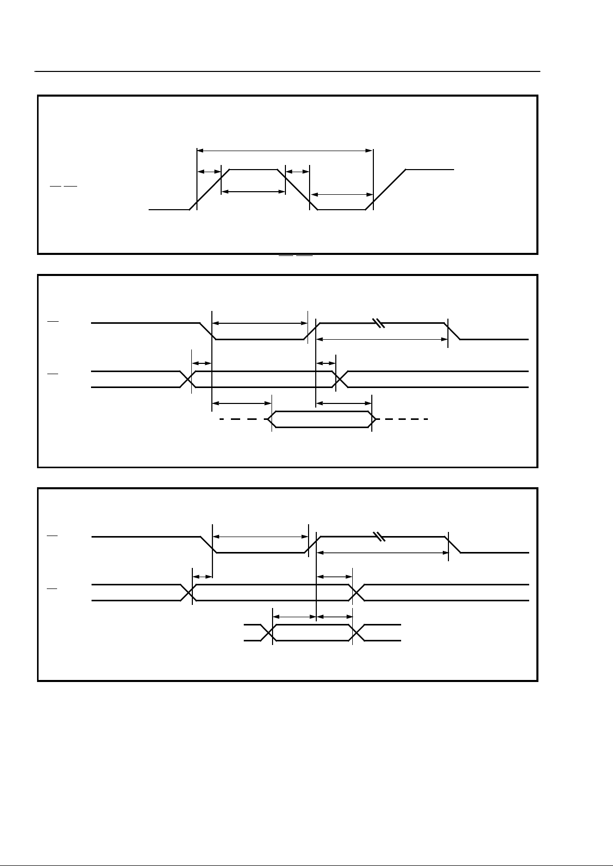
Figure 1 6 - RD/WR Clock Pulse
Figure 17 - 8 031/ 8051/ 8085 Read Tim ing Dia gram
Figure 18 - 80 31/8 051 /8085 Wri te Timin g D iagra m
t
CYC
t
R
t
PWH
t
PWL
RD/WR
t
F
RD
CS, RS0
DATA BUS
t
PWL
t
AS
t
AH
t
PWH
t
DDR
t
DHR
RD
CS, RS0
DATA BUS
t
PWL
t
AS
t
AH
t
PWH
t
DSW
t
DHW
 Loading...