

Page 1

CMOS
MT8841
Calling Number Identification Circuit
Features
• 1200 baud BELL 202 and CCITT V.23
Frequen cy Shift K eying (FSK) demo dulati on
• Comp atible with Bell core TR -NW T-000030 and
SR-TSV-002476
• High inpu t s ensitivi ty: -36dB m
• Simple serial 3-wire data interface eliminating
the need for a UA RT
• Power do wn mo de
• Intern al gain ad ju stable a mp lifie r
• Carrie r dete ct statu s outp ut
• Uses 3.579545 MHz crystal or ceramic
resonator
• Single 5V powe r supp ly
• Low pow er CMO S tech nolog y
Applications
• Calling Num ber De livery (CND), Ca lling Na me
Delivery (CNAM) and Calling Identity on Call
Waiting (CIDCW) feat ures of Bellcore CL A SS
service
• Featur e ph ones
• Phone s et adj unc t boxes
• FAX machines
• Telephone An swer ing m achine s
• Database query systems
SM
ISSUE 4 May 1995
Ordering Information
MT8841AE 16 Pin Plastic D IP
MT8841AS 16 Pin SOIC
MT8841A N 20 Pin SSO P
-40 °C to +85 °C
Description
The MT8841 Calling Number Identification Circuit
(CNIC) is a CMOS integrated circuit providing an
interface to various calling line information delivery
services that utilize 1200 baud BELL 202 or CCITT
V.23 FSK voiceband data transmission schemes.
The CNIC receives and demodulates the signal and
outputs d ata i n to a simple 3-w ire se r ial i n terface.
Typically, the FSK modulated data containing
information on the calling line is sent before alerting
the called par ty or during the silent interval between
the first and second ring using either CCITT V.23
recommendations or Bell 202 specifications.
The CNIC accepts and demodulates both CCITT
V.23 and BELL 202 signals. Along with serial data
and clock, the CNIC provides a data ready signal to
indicate the reception of every 8-bit character sent
from the Central Office. The received data can be
processed externally by a microcontroller, stored in
memory, or displayed as is, depending on the
application.
GS
IN-
IN+
CAP
V
Ref
CLASSSM is a service mark o f B ellcore
-
+
Bias
Generator
PWDN OSC1 OSC2
Receive
Bandpass
Filter
Clock
Generat or
FSK
Demodulator
Figure 1 - Functional Block Diagram
Carrier
Detector
to other
circuits
Data and Timin g
V
SSVDD
Recovery
IC1 IC2
DATA
DR
DCLK
CD
5-11
Page 2

MT8841
1
IN+
2
IN-
3
GS
VRef
CAP
OSC1
OSC2
VSS
4
5
6
7
8
16 PIN PLASTIC DIP/SOIC
16
15
14
13
12
10
1
VDD
IC2
IC1
PWDN
CD
11
DR
DATA
9
DCLK
IN+
IN-
GS
VRef
CAP
NC
OSC1
NC
OSC2
VSS
2
3
4
5
6
7
8
9
10
20 PIN SSOP
20
19
18
17
16
15
14
13
12
11
VDD
IC2
NC
NC
IC1
PWDN
CD
DR
DATA
DCLK
Figure 2 - Pin Connections
Pin Description
Pin #
Name Description
16 20
11 IN+Non-inverting Op-Amp (Input).
22 IN-Inverting Op-Amp (Input).
33 GSGai n Sel ect (Outpu t). Gives access to op-amp out put for connection of feedback resistor.
44 V
Voltage Reference (Output). Nominally V
Ref
55 CAPCapacitor. Connect a 0.1µF capacitor to V
67OSC1Oscillator (Input). Crystal or ceramic resonator connection. This pin can be driven directly
from an external clocking source.
79OSC2Oscillator (Output). Crystal or ceramic resonator connection. When OSC1 is driven by an
external clock, this pin should b e left open.
. This is used to bias the op-amp inputs.
DD/2
.
SS
810 V
Power supply ground.
SS
9 11 DCLK Data Clock (Output). Outputs a clock burst of 8 low going pulses at 1202.8Hz (3.5795MHz
divided by 2976). Every clock burst is initiated by the DATA stop bit start bit sequence. When
the input DATA is 1202.8 baud, the positive edge of each DCLK pulse coincides with the
middle of the data bits output at the DATA pin. No DCLK pulses are generated during the start
or stop bits. Typically, DCLK is used to clock the eight data bits from the 10 bit data word into a
serial-to-parallel converter.
10 12 DATA Data (Outp ut). Serial dat a output correspondi ng to the FSK inpu t and switching at the input
baud rate. Mark frequency at the input corresponds to a logic high, while space frequency
corresponds to a logic low at the DATA output. With no FSK input, DATA is at logic high. This
has become active.
11 13 DR
output stay s high un til CD
Data Ready (Open Drain Output ). This output goes low after the last DCLK pulse of each
word. This can be used to identify the data (8-bit word) boundary on the serial output stream.
Typically, DR
is used to latch the eight data bits from the serial-to -p arallel converter into a
microcontroller.
12 14 CD
Carrier Detect (Open Drain Output). A logic low indicates that a carrier has been present for
a specified time on the line. A time h ysteresis is provided to allow for mom ent ary di sconti nuit y
of carrier.
13 15 PW DN Power Down (Input). Active high, Schmitt Trigger input. Powers down the device including the
input op-amp and the oscillator.
14 16 IC1 Internal Connection 1. Connect to V
SS
.
15 19 IC2 Internal Connection 2. Internally connected, leave open circuit.
16 20 V
6,8
17,
18
Positive power supply voltage.
DD
NC No Connection.
5-12
Page 3

Functional Description
The MT8841 Calling Number Identification Circuit
(CNIC) is a device compatible with the Bellcore
proposal (TR-NWT-000030) on generic requirements
for transmitting asynchronous voiceband data to
Customer Premises Equipment (CPE) from a serving
Stored Program Controlled Switching System
(SPCS) or a Central Office (CO). This data
transmission technique is applicable in a variety of
services like Calling Number Delivery (CND), Calling
Name Delivery (CNAM) or Calling Identity Delivery
on Call Waiting (CIDCW) as specified in Custom
Local Area Signalling Service (CLASS
information delivery features by Bellcore.
With CND, CNAM and CIDCW service, the called
subscriber has the capability to display or to store
the information on the calling party which is sen t by
the CO and received by the CNIC.
SM
) calling
MT8841
IN+
C
VOLTAGE GAIN
) = RF / R
(A
V
R
IN
R
F
IN
Figure 4 - Single-Ended Input Configuration
at the called subscriber location either in the on-hook
case as in CND, or the off-hook case, as in
CIDCW. The functional block diagram of the CNIC
is shown in Figure 1. Note however, for CIDCW
applications, a separate CAS (CPE Alerting Signal)
detector is required.
IN-
GS
V
Ref
MT8841
In the CND service, information about a calling party
is embedded in the silent interval between the first
and second ring. During this period, the CNIC
receives and demodulates the 1200 baud FSK signal
(compatible with Bell-202 specification) and outputs
data into a 3 - wir e se ria l i n te rface.
In the CIDCW service, information about a second
calling party is sent to the subscriber, while they are
engaged in another call. During this period, the CNIC
receives and demodulates the FSK signal as in the
CND case.
The CNIC is designed to provide the data
transmission interface required for the above service
R1
C1
R4
C2
R3
DIFFERENTIAL INPUT AMPLIFIER
C1 = C2 = 10 nF
R1 = R4 = R5 = 100 kΩ
R2 = 60kΩ, R3 = 37.5 kΩ
R3 = (R2R5) / (R2 + R5)
VOLTAGE GAIN
diff) = R5/R1
(A
V
INPUT IMPEDANCE
2
R1
(Z
diff) = 2
IN
+ (1/ωC)
R5
R2
2
IN+
IN-
GS
V
Ref
MT8841
Figure 3 - Differential Input Configuration
In Europe, Caller ID and CIDCW services are being
proposed. These schemes may be different from
their North American counterparts. In most cases,
1200 baud CCITT V.23 FSK is used instead of Bell
202. Because the CNIC can also demodulate 1200
baud CCITT V.23 with the same performance, it is
suitable for these applications.
Although the main application of the CNIC is to
support CND and CIDCW service, it may also be
used in any application where 1200 baud Bell 202
and/or CCITT V.23 FSK data reception is required.
Input Configuration
The input arrangement of the MT8841 provides an
operational amplifier, as well as a bias source (V
which is u se d to b i as the inputs at V
. Provision is
DD/2
Ref
made for connection of a feedback resistor to the opamp output (GS) for adjustment of gain. In a singleended configuration, the input pins are connected as
shown in Figure 4.
Figure 3 shows the necessary connections for a
differential input configuration.
User Interface
The CNIC provides a powerful 3-pin interface which
can reduce the external hardware and software
requirements. The CNIC receives the FSK signal,
demodulates it, and outputs the extracted data to the
DATA pin. For each received stop bit start bit
sequence, the CNIC outputs a fixed frequency clock
string of 8 pulses at the DCLK pin. Each clock rising
)
5-13
Page 4

MT8841
edge corresponds to the centre of each DATA bit cell
(providing the incoming baud rate matches the DCLK
rate). DCLK is not generated for the stop and start
bits. Consequently, DCLK will clock only valid data
into a peripheral device such as a serial to parallel
shift register or a micro-controller. The CNIC also
outputs an end of word pulse (data ready) at the DR
pin. The data ready signal indicates the reception of
every 10-bit word sent from the Central Office. This
output is typically used t o interrupt a micro-controller.
The three outputs together, eliminate the need for a
UART (Universal Asynchronous Receiver
Transmitter) or the high software overhead of
performing the UART function (asynchronous serial
data rece p tio n) .
Note that the 3-pin interface may also output data
generated by voice since these frequencies are in
the input frequency detection band of the device.
The user may choose to ignore these outputs when
FSK data is not expected, or force the CNIC into its
powerdown mode .
Power Down Mode
For applications requiring reduced power
consumption, the CNIC can be forced into power
down when it is not needed to receive FSK data.
This is done by pulling the PWDN pin high. In
powerdown mode, the crystal oscillator, op-amp and
internal circuitry are all disabled and the CNIC will
not react to the input signal. DATA and DCLK are at
logic high, and DR
at logic high when pulled up with resistors.The CNIC
can be awakened for reception of the FSK signal by
pulling the PWDN pin to ground (see Figure 9).
Carrier Detect
The presence of the FSK signal is indicated by a
logic low at the carrier detect (CD
output has built in hysteresis to prevent toggling
when the received signal is shortly interrupted. Note
that the CD
output is also activated by voice since
these frequencies are in the input frequency
detection band of the device. The user may choose
to ignore this output when FSK data is not expected,
or force the CNI C into its powerdown mode.
and CD are at high impedance or
) output. This
MT8841 MT8841 MT8841
OSC1 OSC2 OSC1 OSC2
3.579 545 MHz
OSC1 OSC2
to th e
nex t MT8841
Figure 5 - Common Crystal Connection
Crystal Oscillator
The CNIC uses a crystal oscillator as the master
timing source for filters and the FSK demodulator.
The crystal specification is as follows:
Frequency:
Frequency tolerance:
Resonance mode
:Parallel
Load capacitance:
Maximum series resistance
Maximum drive level (mW):
3.579545 MHz
±0.1%(-40°C+85°C)
18 pF
: 150 ohms
2 mW
e.g. CTS MP036S
A number of MT8841 devices can be connected as
shown in Figure 5 such that only one crystal is
required. The connection between OSC2 and OSC1
can be D.C. coupled as shown, or A.C. coupled
using 30pF capacitors. Alternatively, the OSC1
inputs on all devices can be driven from a CMOS
buffer (dc coupled) with the OSC2 outputs left
unconnected.
VRef and CAP Inputs
V
is the output of a low impedance voltage source
Ref
equal to V
A 0.1µF capacitor is required between CAP and V
to suppress noise on V
and is used to bias the input op-amp.
DD/2
Ref.
SS
5-14
Page 5
Applications
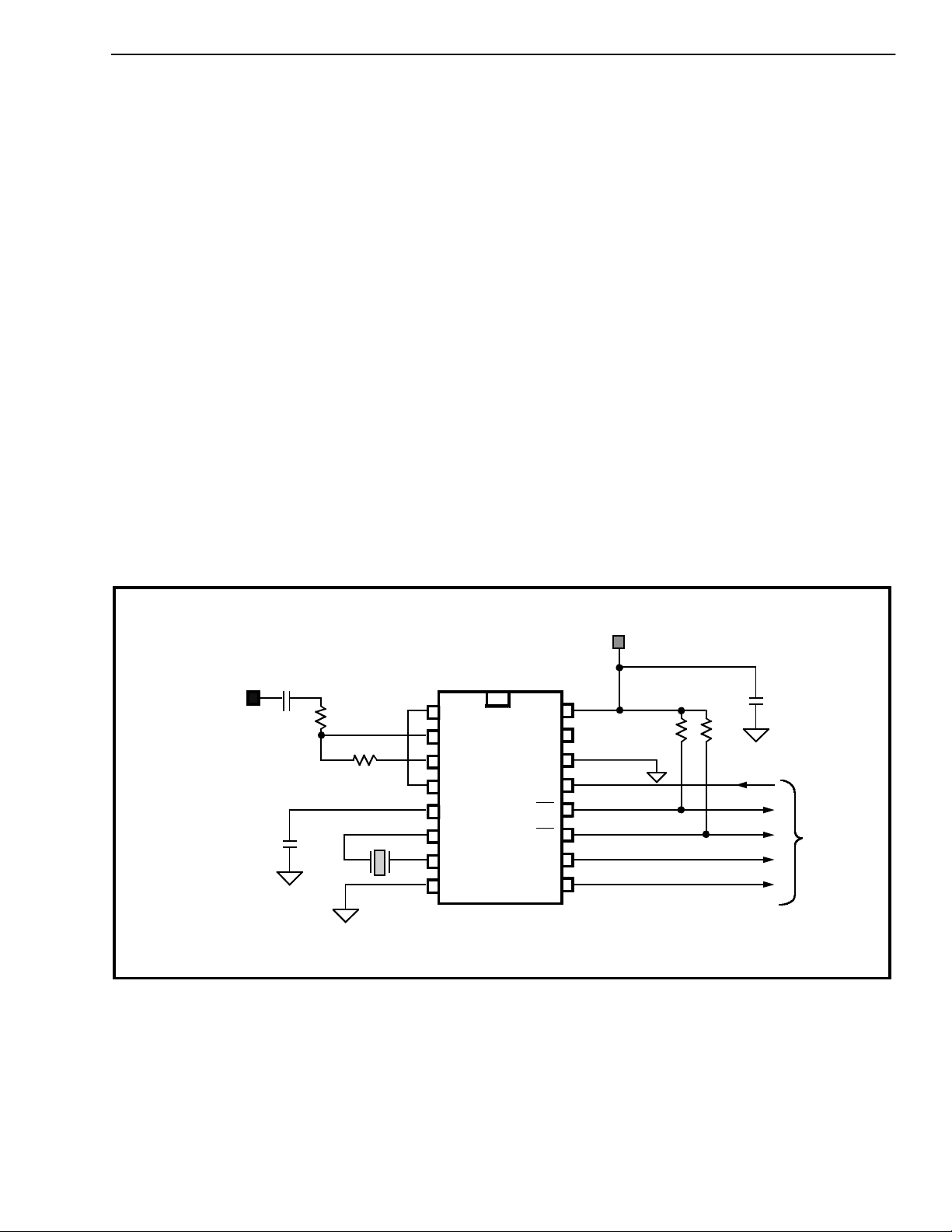
The circuit shown in Figure 6 illustrates the use of
the MT8841 device in a typical FSK receiver system.
Bellcore Special Report SR-TSV-002476 specifies
that the FSK receiver should be able to receive FSK
signal levels as follows:
Received Signal Level at 1200Hz:
-32dBm to - 12d Bm
Received Signal Level at 2200Hz:
-36dBm to - 12d Bm
This condition can be attained by choosing suitable
values of R1 and R2. The MT8841 configured in a
unity gain mode as shown in Fig. 6 meets the above
level requirements.
For applications requiring detection of lower FSK
signal level, the input op amp may be configured to
provide adequate gain.
MT8841
Notes:
R1, R2 = 100 kΩ 1%
R3, R4 = 100 kΩ 10%
C1, C2, C3 = 0.1µF 20%
X-tal = 3.579545 MHz
+5V
IN +
IN GS
VRef
CAP
OSC1
OSC2
VSS
MT8841
VDD
IC2
IC1
PWDN
CD
DR
DATA
DCLK
C1
C2
R1
R2
X-tal
Figure 6 - Application Circuit (Single-Ended Input)
R3
C3
R4
To
Controll er
5-15
Page 6
MT8841
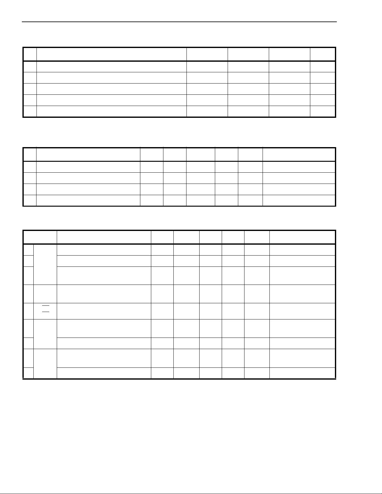
Absolute Maximum Ratings* - Voltages are with respect to V
unless otherwise stated.
SS
Parame ter Symbol Min Max Units
1 DC Power Supply Voltage V
DD
to V
SS
2 Voltage on any pin V
3 Current at any pin (except V
and VSS)I
DD
4 Storage Temperature T
5 Package Power Dissipation P
* Excee di ng these values may cause pe rman ent dama ge . Function al operati on under the se conditi ons is not implie d.
Recommended Operating Conditions - Volt ages are with respect to ground (V
V
DD
P
I/O
ST
D
-0.3 6 V
-0.3 VDD+0.3 V
-65 +150 °C
) unless otherwise stated
SS
Characteristics Sym Min Typ Max Units Test Conditions
1 DC Power Supply Volt age V
2 Clock Frequency f
DD
OSC
4.5 5.0 5.5 V
3.579545
MHz
3 Tolerance on Clock Frequency ∆fc ±0.2 %
4 Operating Temperatu re -40 +85
DC Electrical Characteristics
†
°C
±10 mA
500 mW
Characteristics Sym Min Typ* Max Units Test Conditions
S
1
2 Operating Supply Current I
3 Power Consumption PO 28 mW
4
DATA
DCLK
5
6
PWDN
7 Input Current I
8
9 Output Resista nce R
† DC Electrical Characteristics are over recommended operating conditions unless otherwise stated.
* Typical figures are at 25°C and are for design aid only.
Standby Supply Current IDDQ 15 100 µAPWDN=V
U
P
P
L
Y
Low Level Output Voltage
High Level Output Voltage
DR
Sink Current I
CD
Low Level Input Voltage
High Level Input Voltage
Output Voltage V
VRef
DD
V
OL
OH
OL
IN
Ref
Ref
VDD-0.4
2.5 mA VOL=0.4V
IL
VDD-1.2
IH
2.45 2.5 2.5 5 V VDD=5.0V
V
V
V
35mAPWDN=V
0.4 VVIOL=2.5mA
1.2 V
10 µAVSS ≤ V
2kΩ
V
I
=0.8mA
OH
No Load
IN
DD
SS
≤ V
DD
5-16
Page 7
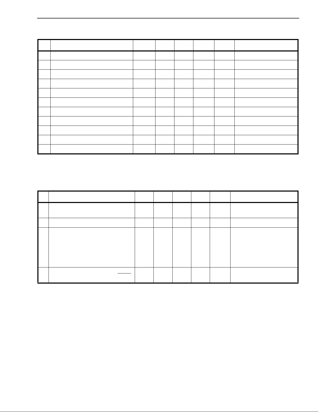
Electrical Characteristics† - Gain Setting Amplifier
Characteristi cs Sym Min Typ
‡
Max Units Test Con ditio ns
MT8841
1 Input Leakage Current I
2 Input Resistance R
3 Input Offset Voltage V
IN
OS
in
5MΩ
1 µAVSS ≤ VIN ≤ V
25 mV
4 Power Supply Rejectio n Ratio PSRR 30 40 dB 1kHz ripple on V
5 Common Mode Rejection CMRR 30 40 dB V
6 DC Open Loop Voltage Gain A
7 Unity Gain Bandwidth f
8 Output Voltage Swing V
9 Maximum Capacitive Load (GS ) C
10 Maximum Resistive Load (GS) R
1 1 Common Mode Range Voltage V
† Electrical characteristics are over recommended operating condition s, unles s otherwise stated.
‡ Typical figures are at 25°C and are for design aid only: not guaran teed and no t subject to producti on testing .
VOL
C
O
L
L
CM
30 32 dB
.2 0.3 MHz
0.5
VDD-0.5
V
100 pF
50 kΩ
1.0
VDD-1.0
V
pp
≤ VIN ≤ V
CMmin
Load ≥ 50kΩ
AC Electrical Characteristics† - FSK Detection
Characteristics Sym Min Typ‡Max Units Notes*
DD
DD
CMmax
1 Input Detection Level -36
12.3
-9
275
dBmmV1, 2, 3
1, 2, 3
2 Input Baud Rate 1188 1200 1212 baud 7
3 Input Frequency Detection
Bell 202 1 (Mark)
Bell 202 0 (Space)
CCITT V. 23 1 (Mar k)
CCITT V.23 0 (Space)
4 Input Noise Tolerance
† AC Electrical Characteristics are over recommended operating conditions, unless otherwise stated.
‡ Typical figures are at 25°C and are for design aid only: not guaran teed and no t subject to producti on testing .
20 log( SNR 20 dB 2, 3, 4, 5
signal
noise
)
1188
2178
1280.5
2068.5
1200
2200
1300
2100
1212
2222
1319.5
2131.5
Hz
}7 BELL 202 Frequencies
Hz
Hz
}7 CCITT V.23 Frequencies
Hz
5-17
Page 8
MT8841
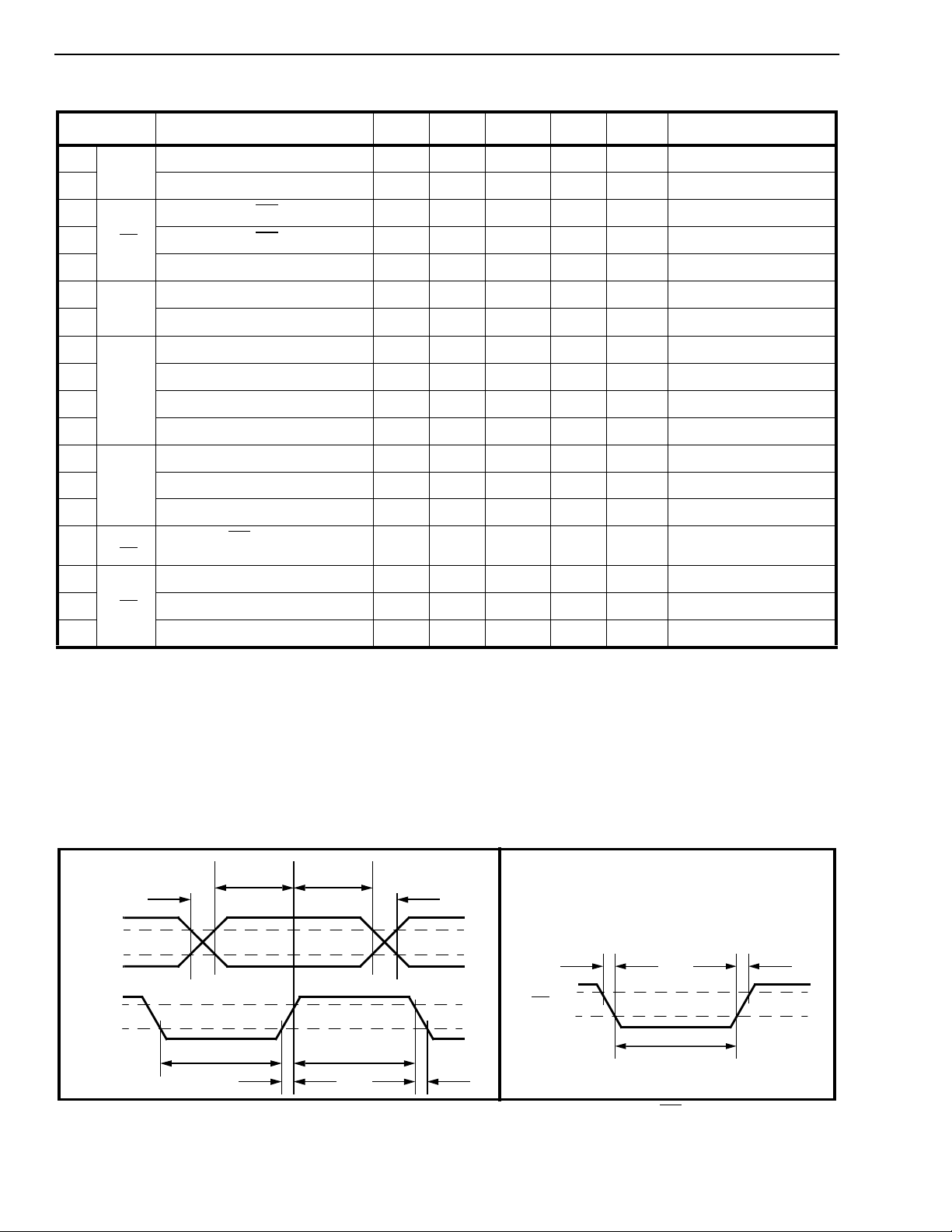
AC Electrical Characteristics† - Timing
Characteristics Sym Min Typ
‡
Max Units Notes*
1
PWDN
OSC1
2 Power-down time t
3
4 Input FSK to CD
Power-up time t
Input FSK to CD low delay t
CD
high delay t
PU
PD
IAL
IAH
8ms
35 50 ms
100 1000 µs 11
25 ms
5 Hysteresis 8 ms
DATA
6
7 Input FSK to DATA delay t
8
9 Fall time t
DATA
DCLK
10 DATA to DCLK delay t
11 DCLK to DATA delay t
12
DCLK
13 High time t
14 Low time t
DCLK
15
16
17 Fall time t
18 Low time t
† AC Electrical Characteristics are over recommended operating conditions unless otherwise stated.
‡ Typical figures are at 25°C and are for design aid only, not guaranteed and not subject to production testin g.
*Notes:
1. dBm=d e ci be ls ab o ve or below a referenc e power of 1m W in to 600Ω.
2. Using un it y ga in te st ci r c uit s ho wn in Figu re 6 .
3. Mark an d S pa c e f r eq ue nc ie s have the s am e am pl itude.
4. Band lim i ted r a nd om n oi se ( 2 00 - 32 0 0Hz ) .
5. Referenced to the mini mu m in pu t detecti on le v el.
6. FSK input data at 1200 ±12 baud.
7. OSC1 at 3.579545 MHz ±0.2%.
8. 10k to V
9. 10k to VDD, 50pF to VSS.
10. Function of sign al con ditio n.
11. The device w il l s to p f un ct io ni ng w it hin this time, but mor e tim e m ay be re quired to rea c h I
12. For a repeating mark space sequence, the data st ream will typically have equal 1 and 0 bit durations.
Rate 118 8 1200 1212 bps 6,12
15ms
200 ns 8
200 ns 8
Rise time t
IDD
R
F
DCD
CDD
6 416 µs 6, 7, 10
6 416 µs 6, 7, 10
Frequency 1200 1202.8 1205 Hz 7
415 416 417 µs 7
415 416 417 µs 7
415 416 417 µs 7
10 µs 9
200 ns 9
415 416 417 µs 7
DCLK to DR delay t
DR
Rise time t
DR
, 50pF to V
SS
SS.
CH
CL
CRD
RR
FF
RL
DDQ
.
5-18
t
CDD
t
CH
t
F
t
FF
DR
t
RL
t
F
DATA
DCLK
t
DCD
t
R
t
CL
t
R
Figure 7 - DATA and DCLK Output Timing Figure 8 - DR Outp ut Timin g
t
RR
Page 9
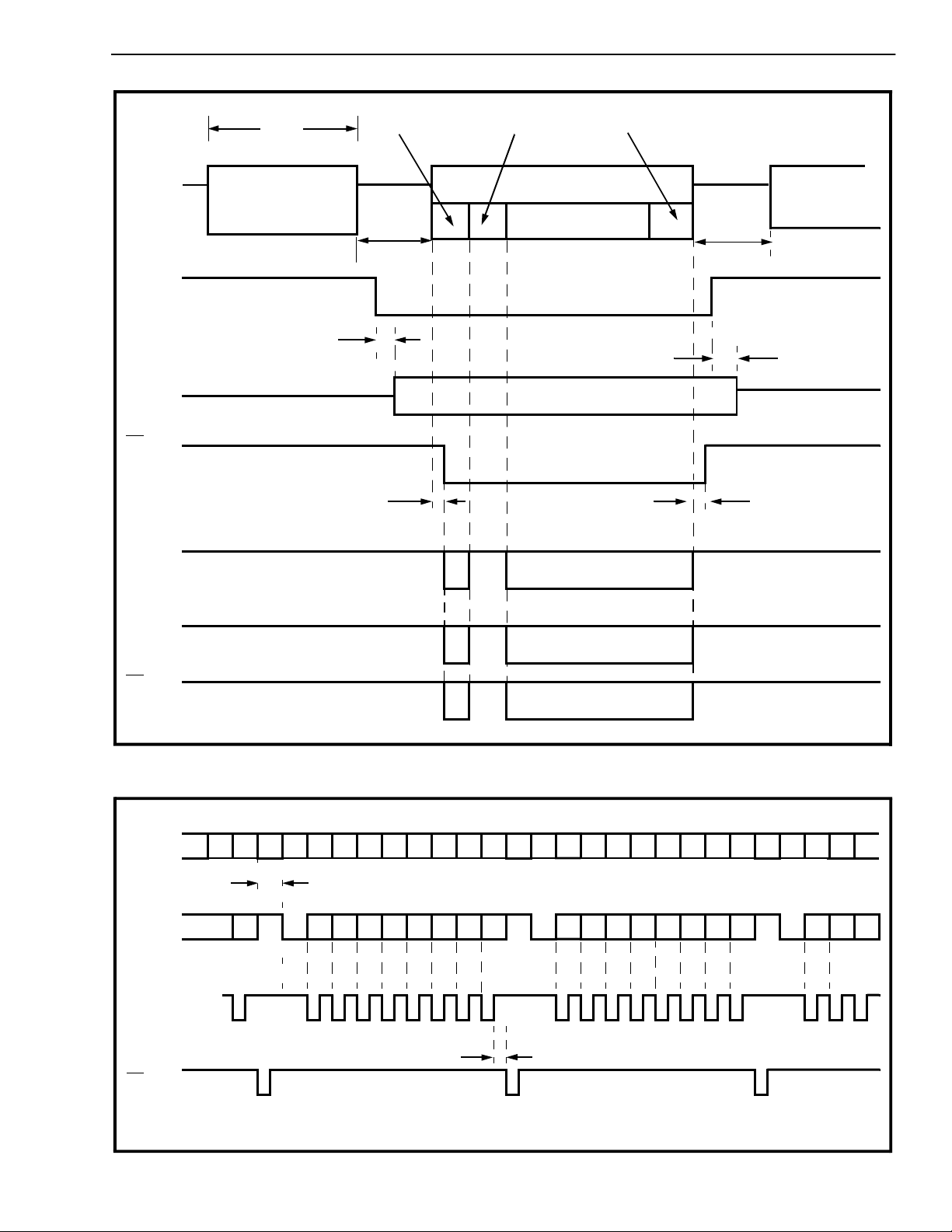
MT8841
TIP/RING
PWDN
OSC2
CD
*
DATA
2 sec
First Ringing
High (Input Idle)
t
PU
channel seizure
500ms
(min)
t
IAL
Mark state checksum
Input FSK
Data
200ms
(min)
t
IAH
High (Input Idle)
t
PD
Second
Ringing
DCLK
DR
*
* with extern al pull-up resistor
start
stop
TIP/RING
DATA
DCLK
b7
10
t
IDD
b7 b0 b1 b2 b3 b4 b5
stop
Figure 9 - Input and Output Timing (Bellcore CND Service)
start
stop
b0 b1 b2 b3 b4 b5
start
b6
b7
b6
b7 b0 b1 b2 b3 b4 b5
b0 b1 b2 b3 b4 b5
10
start
stop
t
CRD
b6
b7
b6
start
stop
10
b7
stop
b0 b1 b2
start
b0 b1 b2
*
DR
* with external pull-up resistor
Figure 10 - Serial Data Interface Timing
5-19
Page 10

MT8841
NOTES:
5-20
 Loading...