

Page 1

M
T6229 / MT6230 GSM/GPRS/EDGE Baseband Processor Data Sheet Revision 2.01
GS
M
T6229 / MT6230
M/GPRS/EDGE Baseband
Processor
Data Sheet
Re
vision 2.01
Nov 3, 2006
1
/667 MediaTek Inc. Confidential
Page 2

M
T6229 / MT6230 GSM/GPRS/EDGE Baseband Processor Data Sheet Revision 2.01
Revision History
R
evision
1.00 Mar 16, 2006 Initial Release
2.00 Sep 12, 2006 Add MT6230 product branch
2.01 Nov 3, 2006 Modify TV-out description on MT6230 product branch
Date Comments
2
/667 MediaTek Inc. Confidential
Page 3

M
T6229 / MT6230 GSM/GPRS/EDGE Baseband Processor Data Sheet Revision 2.01
TABLE OF CONTENTS
R
evision History...................................................................................................................................... 2
1. System Overview............................................................................................................................... 5
1.
1 Platform Features ....................................................................................................................................................... 8
1.2 MODEM Features.................................................................................................................................................... 10
1.3 Multi-Media Features................................................................................................................................................11
1.4 General Description ................................................................................................................................................. 14
2 Product Descriptions ...................................................................................................................... 16
2.1 Pin Outs.................................................................................................................................................................... 16
2.2 Top Marking Definition ........................................................................................................................................... 19
DC Characteristics............................................................................................................................................................. 19
DC Characteristics............................................................................................................................................................. 20
2.3 Pin Description......................................................................................................................................................... 21
3 Micro-Controller Unit Subsystem ................................................................................................. 35
3.
1 Processor Core ......................................................................................................................................................... 36
3.2 Memory Management .............................................................................................................................................. 36
3.3 Bus System............................................................................................................................................................... 40
3.4 Direct Memory Access............................................................................................................................................. 43
3.5 Interrupt Controller .................................................................................................................................................. 61
3.6 Code Cache Controller ............................................................................................................................................. 77
3.7 MPU......................................................................................................................................................................... 86
3.8 Data Cache ............................................................................................................................................................... 95
3.9 Internal Memory Interface ..................................................................................................................................... 105
3.10 External Memory Interface .................................................................................................................................... 105
4 Microcontroller Peripherals ........................................................................................................ 115
4.
1 Pulse-Width Modulation Outputs............................................................................................................................115
4.2 Alerter .....................................................................................................................................................................118
4.3 SIM Interface ......................................................................................................................................................... 120
4.4 Keypad Scanner ..................................................................................................................................................... 130
4.5 General Purpose Inputs/Outputs ............................................................................................................................ 132
4.6 General Purpose Timer........................................................................................................................................... 148
4.7 UART..................................................................................................................................................................... 151
4.8 IrDA Framer........................................................................................................................................................... 166
4.9 Real Time Clock .................................................................................................................................................... 175
4.10 Auxiliary ADC Unit ............................................................................................................................................... 181
4.11 I2C / SCCB ............................................................................................................................................................ 184
4.12 Cipher Hash Engine (CHE).................................................................................................................................... 189
5 Microcontroller Coprocessors ..................................................................................................... 198
5.
1 Divider ................................................................................................................................................................... 198
5.2 CSD Accelerator .................................................................................................................................................... 200
5.3 FCS Codec ............................................................................................................................................................. 212
5.4 PPP Framer Coprocessor (PFC)................................................................................................................................. 214
6 Multi-Media Subsystem ............................................................................................................... 219
6.
1 LCD Interface ........................................................................................................................................................ 219
6.2 NAND FLASH interface ....................................................................................................................................... 241
6.3 USB OTG Controller ............................................................................................................................................. 258
6.4 Memory Stick and SD Memory Card Controller ................................................................................................... 276
6.5 Graphic Memory Controller................................................................................................................................... 300
6.6 2D acceleration ...................................................................................................................................................... 303
3
/667 MediaTek Inc. Confidential
Page 4

M
T6229 / MT6230 GSM/GPRS/EDGE Baseband Processor Data Sheet Revision 2.01
6.7 C
6.8 Drop Resize............................................................................................................................................................ 334
6.9 Post Resize ............................................................................................................................................................. 337
6.10 JPEG Decoder ........................................................................................................................................................ 351
6.11 JPEG Encoder ........................................................................................................................................................ 363
6.12 GIF Decoder........................................................................................................................................................... 369
6.13 PNG Decoder......................................................................................................................................................... 380
6.14 Camera Interface .................................................................................................................................................... 391
6.15 Image DMA ........................................................................................................................................................... 444
6.16 Image Engine ......................................................................................................................................................... 475
6.17 MPEG-4/H.263 Video CODEC ............................................................................................................................. 495
6.18 TV Controller ......................................................................................................................................................... 535
6.19 TV encoder............................................................................................................................................................. 541
apture Resize ....................................................................................................................................................... 325
7 Audio Front-End........................................................................................................................... 550
7.
1 General Description ............................................................................................................................................... 550
7.2 Register Definitions ............................................................................................................................................... 553
7.3 Programming Guide ............................................................................................................................................... 557
8 Radio Interface Control ............................................................................................................... 559
8.1 Baseband Serial Interface....................................................................................................................................... 559
8.2 Baseband Parallel Interface.................................................................................................................................... 567
8.3 Automatic Power Control (APC) Unit ................................................................................................................... 571
8.4 Automatic Frequency Control (AFC) Unit ............................................................................................................ 577
8.5 Baseband Serial Ports............................................................................................................................................. 579
9 Baseband Front End..................................................................................................................... 584
9.
1 Downlink Path (RX Path) ...................................................................................................................................... 585
9.2 Uplink Path (TX Path) ........................................................................................................................................... 593
10 Timing Generator ......................................................................................................................... 601
10.1 TDMA timer........................................................................................................................................................... 601
10.2 Slow Clocking Unit................................................................................................................................................ 610
11 Power, Clocks and Reset .............................................................................................................. 613
11.1 B2PSI ..................................................................................................................................................................... 613
11.2 Clocks .................................................................................................................................................................... 615
11.3 Reset Management ................................................................................................................................................. 621
11.4 Software Power Down Control .............................................................................................................................. 625
12 Analog Front-end & Analog Blocks ............................................................................................ 630
12
.1 General Description ............................................................................................................................................... 630
12.2 MCU Register Definitions ..................................................................................................................................... 641
12.3 Programming Guide ............................................................................................................................................... 652
13 Digital Pin Electrical Characteristics.......................................................................................... 663
4
/667 MediaTek Inc. Confidential
Page 5

M
T6229 / MT6230 GSM/GPRS/EDGE Baseband Processor Data Sheet Revision 2.01
1. System Overview
B
oth MT6229 and MT6230 are feature-rich and extremely
powerful single-chip solutions for high-end mobile phones
with GSM/GPRS and EDGE capability. Based on 32 bit
ARM7EJ-STM RISC processor, MT6229 / MT6230’s
superb processing power along with high bandwidth
architecture and dedicated hardware support provides an
unprecedented platform for high performance EGPRS
Class 12 MODEM and leading-edge multimedia
applications. To sum up, MT6229 / MT6230 both present a
revolutionary platform for multimedia-centric mobile
devices along with an EDGE capable modem.
Flash, page mode SRAM, and Pseudo SRAM are also
supported. For greatest compatibility, the memory interface
can also be used to connect to legacy devices such as
Color/Parallel LCD, and multi-media companion chip are
all supported through this interface. To minimize power
consumption and ensure low noise, this interface is
designed for flexible I/O voltage and allows lowering of
supply voltage down to 1.8V. The driving strength is
configurable for signal integrity adjustment. The data bus
also employs retention technology to prevent the bus from
floating during turn over.
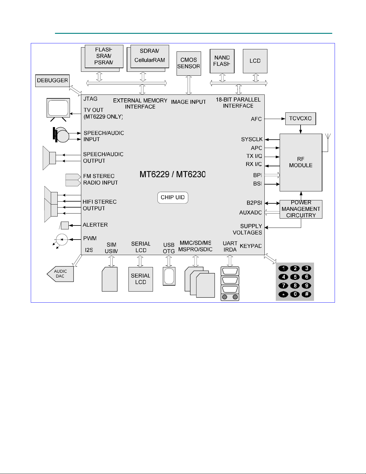
Typical application diagram is shown in Figure 1.
Platform
M
ARM7EJ-STM RISC processor at up to 104Mhz, thus
providing fast data processing capabilities. In addition to
the high clock frequency, separate CODE and DATA
caches are also added to further improve the overall system
efficiency.
For large amount of data transfer, high performance DMA
(Direct Memory Access) with hardware flow control is
implemented, which greatly enhances the data movement
speed while reducing MCU processing load.
Targeted as a media-rich platform for mobile applications,
MT6229 and MT6230 also provide hardware security
digital rights management for copyright protection. For
further safeguarding, and to protect manufacturer’s
development investment, hardware flash content protection
is also provided to prevent unauthorized porting of
software load.
Memory
T
maximum bandwidth for data intensive applications such
as multimedia features, MT6229 and MT6230 support up
to 4 external state-of-the-art devices through its 8/16-bit
host interface. High performance devices such as Mobile
RAM, and Cellular RAM are supported for maximum
bandwidth. Traditional devices such as burst/page mode
T6229 and MT6230 are capable of running the
o provide the greatest capacity for expansion and
Multi-media
he MT6229 multi-media subsystem provides connection
T
to CMOS image sensor and supports resolution up to 3M
pixels, while MT6230 supports up to 1.3M pixels. With
their advanced image signal and data processing
technology, both MT6229 and MT6230 allow efficient
processing of image and video data. MT6229 and MT6230
also have built-in JPEG CODEC and MPEG-4/H.263
CO
DEC, thus enabling real-time recording and playback
of high-quality images and video. Hardware
MPEG4/H.263 accelerator supports playback in VGA
mode at 15fps, and encoding in CIF at 15fps. Videophone
functionality is also provided. Moreover, high quality
de-blocking filter is provided to remove blocking artifacts
in video playback. GIF decoder and PNG decoder are
implemented as well for fast image decoding. MT6229 and
MT6230 also support TV-OUT capability, thus allowing
the mobile handset to connect to TV screen via NTSC/PAL
connections.
In addition to advanced image and video features, MT6229
and MT6230 also utilize high resolution audio DAC,
digital audio, and audio synthesis technology to provide
superior audio features for all future multi-media needs.
Connectivity, and Storage
n order to take advantage of its incredible multimedia
I
strengths, MT6229 and MT6230 incorporate myriads of
advanced connectivity and storage options for data storage
and communication. MT6229 and MT6230 support UART,
5
/667 MediaTek Inc. Confidential
Page 6

M
T6229 / MT6230 GSM/GPRS/EDGE Baseband Processor Data Sheet Revision 2.01
Fast IrDA, USB 1.1 Full Speed OTG, SDIO, Bluetooth and
W
IFI Interface, and MMC/SD/MS/MS Pro storage
systems. All these interfaces provide MT6229 / MT6230
users with the highest degree of flexibility in implementing
solutions suitable for the targeted application.
To achieve a complete user interface, MT6229 / MT6230
also bring together all the necessary peripheral blocks for a
multi-media 2.75G phone. The peripheral blocks includes
the Keypad Scanner with the capability to detect multiple
key presses, SIM Controller, Alerter, Real Time Clock,
PWM, Serial LCD Controller, and General Purpose
Programmable I/Os.
Furthermore, to provide more configuration and bandwidth
for multi-media products, an additional 18-bit parallel
interface is incorporated. This interface enables connection
to LCD panels as well as connection to NAND flash
devices for additional multi-media data storage.
Audio
sing a highly integrated mixed-signal Audio Front-End,
U
architecture of both MT6229 and MT6230 allow for easy
audio interfacing with direct connection to the audio
transducers. The audio interface integrates D/A and A/D
Converters for Voice band, as well as high resolution
Stereo D/A Converters for Audio band. In addition,
MT6229 / MT6230 also provide Stereo Input and Analog
Mux.
expensive TCVCXO. MT6229 / MT6230 achieve great
MODEM performance by utilizing 14-bit high resolution
A/D Converter in the RF downlink path. Furthermore, to
reduce the need for extra external current-driving
component, the driving strength of some BPI outputs is
designed to be configurable.
Debug Function
T
he JTAG interface enables in-circuit debugging of
software program with the ARM7EJ-S core. With this
standardized debugging interface, MT6229 and MT6230
provide developers with a wide set of options in choosing
ARM development kits from different third party vendors.
Power Management
T6229 and MT6230 offer various low-power features to
M
help reduce system power consumption. These features
include Pause Mode of 32KHz clocking at Standby State,
Power Down Mode for individual peripherals, and
Processor Sleep Mode. In addition, MT6229 and MT6230
are also fabricated in advanced low leakage CMOS process,
hence providing an overall ultra low leakage solution.
Package
T
he MT6229 and MT6230 devices are offered in a
13mm×13mm, 314-ball, 0.65 mm pitch, TFBGA package.
MT6229 and MT6230 support AMR codec to adaptively
optimize speech and audio quality. Moreover, HE-AAC
codec is implemented to deliver CD-quality audio at low
bit rates.
On the whole, MT6229 and MT6230’s audio features
provide a rich solution for multi-media applications.
Radio
oth MT6229 / MT6230 integrate a mixed-signal
B
Baseband front-end in order to provide a well-organized
radio interface with flexibility for efficient customization.
It contains gain and offset calibration mechanisms, and
filters with programmable coefficients for comprehensive
compatibility control on RF modules. This approach also
allows the usage of a high resolution D/A Converter for
controlling VCXO or crystal, thus reducing the need for
6
/667 MediaTek Inc. Confidential
Page 7
M
T6229 / MT6230 GSM/GPRS/EDGE Baseband Processor Data Sheet Revision 2.01
Figure
7
1 Typical application of MT6229 / MT6230.
/667 MediaTek Inc. Confidential
Page 8

M
T6229 / MT6230 GSM/GPRS/EDGE Baseband Processor Data Sheet Revision 2.01
1.1 Platform Features
General
Integrated voice-band, audio-band and base-band
analog front ends
TFBGA 13mm×13mm, 313-ball, 0.65 mm pitch
package
MCU Subsystem
ARM7EJ-S 32-bit RISC processor
High performance multi-layer AMBA bus
Java hardware acceleration for fast Java-based
ga
mes and applets
Operating frequency: 26/52/104 MHz
Dedicated DMA bus
14 DMA channels
1M bits on-chip SRAM
1M bits MCU dedicated Tightly Coupled memory
256K bits CODE cache
Industry standard Parallel LCD Interface
Supports multi-media companion chips with 8/16
ts data width
bi
Flexible I/O voltage of 1.8V ~ 2.8V for memory
interface
Configurable driving strength for memory
interface
User Interfaces
6-row × 7-column keypad controller with
hardware scanner
Supports multiple key presses for gaming
SIM/USIM Controller with hardware T=0/T=1
protocol control
Real Time Clock (RTC) operating with a separate
po
wer supply
General Purpose I/Os (GPIOs)
2 Sets of Pulse Width Modulation (PWM) Output
64K bits DATA cache
On-chip boot ROM for Factory Flash
Pr
ogramming
Watchdog timer for system crash recovery
3 sets of General Purpose Timer
Circuit Switch Data coprocessor
Division coprocessor
PPP Framer coprocessor
External Memory Interface
Supports up to 4 external devices
Supports 8-bit or 16-bit memory components with
ma
ximum size of up to 64M Bytes each
Supports Mobile RAM, and Cellular RAM
Supports Flash and SRAM/PSRAM with Page
Mode or Burst Mode
Alerter Output with Enhanced PWM or PDM
8 external interrupt lines
Security
Cipher: supports AES, DES/3DES
Hash: supports MD5, SHA-1
Supports security key and 27 bit chip unique ID
Connectivity
3 UARTs with hardware flow control and speed up
to 921600 bps
IrDA modulator/demodulator with hardware
fr
amer. Supports SIR/MIR/FIR operating speeds.
Full-speed USB 1.1 OTG capability. Supports
device mode, limited host mode, and dual-role
OTG mode.
8
/667 MediaTek Inc. Confidential
Page 9

M
M
ulti Media Card/Secure Digital Memory
T6229 / MT6230 GSM/GPRS/EDGE Baseband Processor Data Sheet Revision 2.01
Card/Memory Stick/Memory Stick Pro host
controller with flexible I/O voltage power
Supports SDIO interface for SDIO peripherals as
we
ll as WIFI connectivity
DAI/PCM and I2S interface for Audio application
Power Management
Power Down Mode for analog and digital circuits
Processor Sleep Mode
Pause Mode of 32KHz clocking at Standby State
7-channel Auxiliary 10-bit A/D Converter for
ch
arger and battery monitoring and photo sensing
Test and Debug
Built-in digital and analog loop back modes for
both Audio and Baseband Front-End
DAI port complying with GSM Rec.11.10
JTAG port for debugging embedded MCU
9
/667 MediaTek Inc. Confidential
Page 10

M
T6229 / MT6230 GSM/GPRS/EDGE Baseband Processor Data Sheet Revision 2.01
1.2 MODEM Features
Radio Interface and Baseband Front End
GMSK/8PSK modulator with analog I and Q
channel outputs
10-bit D/A Converter for uplink baseband I and Q
signals
14-bit high resolution A/D Converter for downlink
baseband I and Q signals
Calibration mechanism of offset and gain
mi
smatch for baseband A/D Converter and D/A
Converter
10-bit D/A Converter for Automatic Power
Control
13-bit high resolution D/A Converter for
Automatic Frequency Control
Programmable Radio RX filter with adaptive
ba
ndwidth control
Dedicated Rx filter for FB acquisition
2 Channels Baseband Serial Interface (BSI) with
3-wire control
Bi-directional BSI interface. RF chip register read
access with 3-wire or 4-wire interface.
10-Pin Baseband Parallel Interface (BPI) with
pr
ogrammable driving strength
GSM/GPRS quad vocoders for adaptive multirate
MR), enhanced full rate (EFR), full rate (FR)
(A
and half rate (HR)
GSM channel coding, equalization and A5/1, A5/2
and A5/3 ciphering
GPRS/EGPRS GEA1, GEA2 and GEA3 ciphering
Programmable GSM/GPRS/EGPRS Modem
Packet Switched Data with CS1-CS4,
MC
S1-MCS9 coding schemes with full set IR
(Incremental Redundancy) support
GSM Circuit Switch Data
GPRS/EGPRS Class 12
Voice Interface and Voice Front End
Two microphone inputs sharing one low noise
am
plifier with programmable gain and automatic
gain control (AGC) mechanism
Voice power amplifier with programmable gain
2nd order Sigma-Delta A/D Converter for voice
uplink path
D/A Converter for voice downlink path
Supports half-duplex hands-free operation
Compliant with GSM 03.50
Multi-band support
Voice and Modem CODEC
Dial tone generation
Voice Memo
Noise Reduction
Echo Suppression
Advanced Sidetone Oscillation Reduction
Digital sidetone generator with programmable
ga
in
Two programmable acoustic compensation filters
1
0/667 MediaTek Inc. Confidential
Page 11

M
T6229 / MT6230 GSM/GPRS/EDGE Baseband Processor Data Sheet Revision 2.01
1.3 Multi-Media Features
LCD/NAND Flash Interface
Dedicated Parallel Interface supports 3 external
devices with 8/16 bit NAND flash interface,
8/9/16/18 bit Parallel Interface, and Serial
interface for LCM
Built-in NAND Flash Controller with 1-bit ECC
for mass storages
Two chip selects available for high-density NAND
fl
ash device
LCD Controller
Supports simultaneous connection to up to 3
parallel LCD and 2 serial LCD modules
Supports LCM format: RGB332, RGB444,
RGB565, RGB666, RGB888
Supports LCD module with maximum resolution
up
to 800x600 at 24bpp
Per pixel alpha channel
True color engine
Supports hardware display rotation
Capable of combining display memories with up to
6 blending layers
Three Gamma correction tables
Image Signal Processor
8/10 bit Bayer format image input
YUV422/YCbCr422/RGB565 image input
Capable of processing image of size up to
MT6229: 3M pixels
MT6230: 1.3M pixels
Color Correction Matrix
Gamma Correction
Automatic Exposure Control
Automatic White Balance Control
Automatic Focus Control
Edge Enhancement
Color Suppression
Cross-talk compensation
Shading compensation
Defect Pixel compensation
Graphic Compression
GIF Decoder
PNG Decoder
JPEG Decoder
ISO/IEC 10918-1 JPEG Baseline and Progressive
modes
Supports all possible YUV formats, including
gr
ayscale format
Supports all DC/AC Huffman table parsing
Supports all quantization table parsing
Supports restart interval
Supports SOS, DHT, DQT and DRI marker
parsing
IEEE Std 1180-1990 IDCT Standard Compliant
Supports progressive image processing to
mi
nimize storage space requirement
Supports reload-able DMA for VLD stream
JPEG Encoder
ISO/IEC 10918-1 JPEG baseline mode
ISO/IEC 10918-2 Compliance
Supports YUV422 and YUV420 and grayscale
fo
rmats
Supports JFIF
Standard DC and AC Huffman tables
Provides 14 levels of encode quality
1
1/667 MediaTek Inc. Confidential
Page 12

M
S
upports continuous shooting
T6229 / MT6230 GSM/GPRS/EDGE Baseband Processor Data Sheet Revision 2.01
Encoder resync marker and HEC
Image Data Processing
Support Digital Zoom
Support RGB888/565, YUV444 image processing
High throughput hardware scaler. Capable of
ta
iloring image to arbitrary size
Horizontal scaling in averaging method
Vertical scaling in bilinear method
Simultaneous scaling for MPEG-4 encode and
LC
D display
YUV and RGB color space conversion
Pixel format transform
Boundary padding
Pixel processing: hue/saturation/intensity/color
adjustment, Gamma correction and
grayscale/invert/sepia-tone effects
Programmable Spatial Filtering: Linear filter,
No
n-linear filter and Multi-pass artistic effects
Hardware accelerated image editing
Photo frame capability
RGB thumbnail data output
Supported visual tools for decoder: I-VOP, P-VOP,
C
/DC prediction, 4-MV, Unrestricted MV, Error
A
Resilience, Short Header
Error Resilience for decoder: Slice
Re
synchronization, Data Partitioning, Reversible
VLC
Supported visual tools for encoder: I-VOP, P-VOP,
Half-pel, DC prediction, Unrestricted MV,
Reversible VLC, Short Header
Supports encoding motion vector of range up
to
–64/+63.5 pixels
HE-AAC decode support
AAC/AMR/HE-AAC audio decode support
AMR audio encode support
TV-OUT
Supports NTSC/PAL formats (interlaced mode)
10 bit video DAC with 2x oversampling
Support one composite video output
2D Accelerator
Supports 32-bpp ARGB8888 and 24bpp RGB888
and 16-bpp RGB565 and 8-bpp index color modes
MPEG-4/H.263 CODEC
Hardware Video CODEC
ISO/IEC 14496-2 simple profile:
de
code @ level 0/1/2/3
encode @ level 0
ITU-T H.263 profile 0 @ level 10
Max decode speed is VGA @ 15fps
Max encode speed is CIF @ 15fps
Support VGA mode encoding
Horizontal and Vertical De-blocking filter in video
pl
ayback
Supports SVG Tiny acceleration
Rectangle gradient fill
BitBlt: multi-BitBlt with 7 rotation, 16 binary ROP
Alpha blending with 7 rotation
Line drawing: normal line, dotted line,
an
ti-aliasing
Circle drawing
Bezier curve drawing
Triangle flat fill
Font caching: normal font, Italic font
Command queue with max depth of 2047
2/667
1
MediaTek Inc. Confidential
Page 13

M
T6229 / MT6230 GSM/GPRS/EDGE Baseband Processor Data Sheet Revision 2.01
A
udio CODEC
Support HE-AAC decode
Wavetable synthesis with up to 64 tones
Advanced wavetable synthesizer capable of
ge
nerating simulated stereo
Wavetable including GM full set of 128
instruments and 47 sets of percussions
PCM Playback and Record
Digital Audio Playback
Audio Interface and Audio Front End
Supports I2S interface
High resolution D/A Converters for Stereo Audio
playback
Stereo analog input for stereo audio source
Analog multiplexer for Stereo Audio
FM Radio Recording
Stereo to Mono Conversion
3/667
1
MediaTek Inc. Confidential
Page 14

M
T6229 / MT6230 GSM/GPRS/EDGE Baseband Processor Data Sheet Revision 2.01
1.4 General Description
F
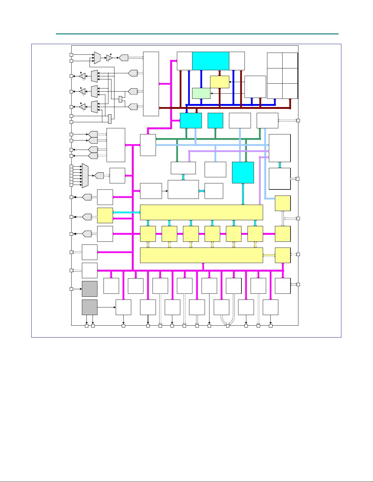
igure 2 details the block diagram of MT6229 and MT6230. Based on a dual-processor architecture, MT6229 / MT6230
i
ntegrate both an ARM7EJ-S core and 2 digital signal processor cores. ARM7EJ-S is the main processor that is responsible
for running high-level 2G to 2.75G protocol software as well as multi-media applications. Digital signal processors handle
the MODEM algorithms as well as advanced audio functions. Except for some mixed-signal circuitries, the other building
blocks in MT6229 and MT6230 are connected to either the microcontroller or one of the digital signal processor.
Specifically, both MT6229 and MT6230 consist of the following subsystems:
Microcontroller Unit (MCU) Subsystem - includes an ARM7EJ-S RISC processor and its accompanying memory
management and interrupt handling logics.
Digital Signal Processor (DSP) Subsystem - includes 2
DSP cores and their accompanying memory, memory
controller, and interrupt controller.
MCU/DSP Interface - where the MCU and the DSPs exchange hardware and software information.
Microcontroller Peripherals - includes all user interface modules and RF control interface modules.
Microcontroller Coprocessors - runs computing-intensive processes in place of Microcontroller.
DSP Peripherals - hardware accelerators for GSM/GPRS/EGDE channel codec.
Multi-media Subsystem - integrates several advanced a
Voice Front End - the data path for converting analog speech from and to digital speech.
Audio Front End - the data path for converting stereo audio from stereo audio source
Video Front End - the data path for converting video signal to NTSL/PAL format.
Baseband Front End - the data path for converting digital signal from and to analog signal of RF modules.
Timing Generator - generates the control signals related to the TDMA frame timing.
Power, Reset and Clock subsystem - manages the power,
ccelerators to support multi-media applications.
reset, and clock distribution inside MT6229 and
MT6230.
Details of the individual subsystems and blocks are described in following Chapters. By default, except CMOS sensor
interface, all features are identical for MT6229 and MT6230, and those descriptions related to MT6229 can also be applied
to MT6230.
4/667
1
MediaTek Inc. Confidential
Page 15
M
T6229 / MT6230 GSM/GPRS/EDGE Baseband Processor Data Sheet Revision 2.01
MIC-0
MIC-1
VOICE
UDIO-L
A
AUDIO-R
STEREO-L
STEREO-R
RX-I
X-Q
R
TX-I
TX-Q
AUXADC
A
APC
ADC
DAC
AUDIO
P
DAC
+
DAC
+
ADC
ADC
BASEBAND
ATH
ADC
TV-OUT
ON
C
P
AUX
DC
A
DAC
DAC
FC
DAC AFC
DACTVOUT
DAC APC
ATH
BRIDGE
INTERRUPT
ONTROL
C
2D
NGINE
E
IMAGE
MA
D
PATCH
U
NITS
MCU/DSP
I
NTERFACE
CACHE
ARM7EJ-S
GRAPHIC MEMORY
IMAGE
OST
P
PROC’
MEMORY
DSP1
ONTROLLER
C
BOOT
R
OM
SECURITY
NGINE
E
TCM
GIF/PNG
ECODE
D
DSP2
JPEG
C
TRAP
U
NITS
C
ONTROL
ODEC
DMA
ON-CHIP
RAM
S
INTERRUPT
ONTROL
C
MPEG-4
IDEO
V
CODEC
USB OTG
COPROC
E
SSOR
COPROC
SSOR
E
COPROC
E
SSOR
CACHE
EXTERNAL
EMORY
M
INTERFACE
NAND
F
COPROC
E
COPROC
E
COPROC
E
LCD
ON
C
LASH
CON
SSOR
SSOR
SSOR
USB OTG
SDRAM
CellularRAM
FLASH
SRAM
PSRAM
NAND
CD
L
SERIAL RF
CONTROL
PARALLEL
RF CONTROL
SYSTEM
LOCK
C
13/26MHZ
BSI
BPI
CLOCK
EN
G
32K
SC
O
32KHZ
CRYSTAL
TDMA
IMER
T
RTC
WAKE UP
GPT
WDT
RESET
Figure 2 M
IMAGE RESIZER
SIM GPIO
PWM
USER
INTERFACE
KEYPAD
ALERTER
B2PSI IRDA
SERIAL
CD
L
SERIAL PORT
T6229 / MT6230 block diagram.
MMC
D/MS
S
MS PRO
C
ONNECTIVITY
UART
IMAGE
IGNAL
S
PROC’
SCCB
M
MT6230
T6229
CMOS
ENSOR
S
5/667
1
MediaTek Inc. Confidential
Page 16

M
T6229 / MT6230 GSM/GPRS/EDGE Baseband Processor Data Sheet Revision 2.01
2 Product Descriptions
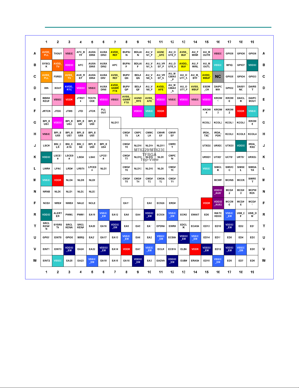
2.1
One type of package for this product, TFBGA 13mm*13mm
MT6229 / MT6230 are pin-to-pin compatible to MT6228 except one VDDK ball @P15.
Pin-outs and the top view are illustrated in Figure 3 for this package. Outline and dimension of package is illustrated in
Figure 4, while the definition of package is shown in Table 1.
Pin Outs
, 314-ball, 0.65 mm pitch Package, is offered. Note that
6/667
1
MediaTek Inc. Confidential
Page 17
M
T6229 / MT6230 GSM/GPRS/EDGE Baseband Processor Data Sheet Revision 2.01
Figure 3 T
op View of MT6229 (MT6230) TFBGA 13mm*13mm, 314-ball, 0.65 mm pitch Package
7/667
1
MediaTek Inc. Confidential
Page 18
M
T6229 / MT6230 GSM/GPRS/EDGE Baseband Processor Data Sheet Revision 2.01
D
E
MT6229 / MT6230
T
op View
(Pins Down)
A C A1
1516171819
MT6229 / MT6230
e b
B
View
15 4 3 2610 9 8 711121314
A
B
C
D
E
F
G
H
J
K
L
M
N
P
R
Y
U
V
W
ottem
Figure 4 Outlines and Dimension of TFBGA 13mm*13mm, 314-ball, 0.65 mm pitch Package
Body Size Ball Count Ball Pitch Ball Dia. Package Thk. Stand Off Substrate Thk.
D E N E
13 13 314 0
B A (Max.) A1 C
.65 0.3 1.2 0.3 0.36
Table 1
Definition of TFBGA 13mm*13mm, 314-ball, 0.65 mm pitch Package (Unit: mm)
8/667
1
MediaTek Inc. Confidential
Page 19
M
T6229 / MT6230 GSM/GPRS/EDGE Baseband Processor Data Sheet Revision 2.01
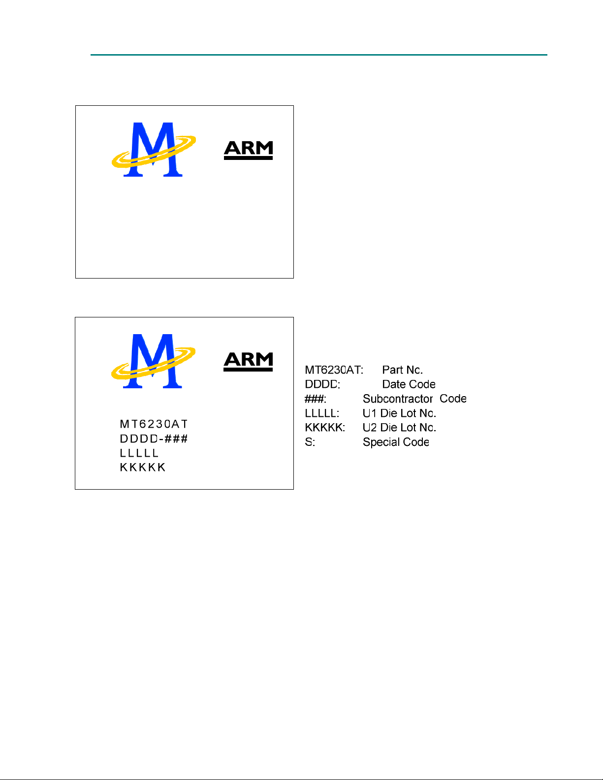
2.2 Top Marking Definition
M T 6 2 2 9 A T
D D D D - # # #
L L L L L
K K K K K
S
MT6229AT: Part No.
DDDD: Date Code
###: Subcontractor Code
LLLLL: U1 Die Lot No.
KKKKK: U2 Die Lot No.
S: Special Code
S
9/667
1
MediaTek Inc. Confidential
Page 20

M
T6229 / MT6230 GSM/GPRS/EDGE Baseband Processor Data Sheet Revision 2.01
DC Characteristics
2
.2.1 Absolute Maximum Ratings
Prolonged exposure to absolute maximum ratings may re
ratings is not implied.
Item Symbol Min Max Unit
IO power supply V
I/O input voltage V
Operating temperature T
Storage temperature T
DD33 -0.3 VDD33+0.3 V
DD33I -0.3 VDD33+0.3 V
opr -20 80 Celsius
stg -55 125 Celsius
duce device reliability. Functional operation at these maximum
0/667
2
MediaTek Inc. Confidential
Page 21

M
T6229 / MT6230 GSM/GPRS/EDGE Baseband Processor Data Sheet Revision 2.01
2.3 Pin Description
elow pin description is identical for both MT6229 and MT6230.
B
Ball
13X13
E4
F5
F4
F3
F2
F1
G5
G4
G3
G1
J6
H5
H4 BPI_BUS6 IO RF hard-wire control bus 6
H3 BPI_BUS7 IO RF hard-wire control bus 7
H2 BPI_BUS8 IO RF hard-wire control bus 4
J5 BPI_BUS9 IO RF hard-wire control bus 5
J4
J3
J2
R4 PWM1 I
R3 PWM2 I
R2 ALERTER IO Pulse width modulated signal for buzzer
J1 LSCK I
K5 LSA0 I
K4 LSDA I
K3 LSCE0# I
K2 LSCE1# I
K6 LPCE1# I
L5
L4
L3
L2
L1
G7 NLD17 I
J9 NLD16 I
K9
J10
L9
K10
J11
L10
K11
N
ame Dir Description
RST#
JT
JT
CK
DI
JT
JT
MS
DO
JT
TCK
JR
PI_BUS0
B
PI_BUS1
B
PI_BUS2
B
PI_BUS3
B
PI_BUS4
B
PI_BUS5
B
SI_CS0
B
SI_DATA
B
SI_CLK
B
PCE0#
L
RST#
L
RD#
L
PA0
L
WR#
L
LD15
N
LD14
N
DL13
N
LD12
N
LD11
N
LD10
N
LD9
N
JTAG Port
I JTAG test port reset input PD Input
I JTAG test port clock input PU Input
I JTAG test port data input PU Input
I JTAG test port mode switch PU Input
O JTAG test port data output 0
O JTAG test port returned clock output 0
RF Parallel Control Unit
O RF hard-wire control bus 0 0
O RF hard-wire control bus 1 0
O RF hard-wire control bus 2 0
O RF hard-wire control bus 3 0
O RF hard-wire control bus 4
O RF hard-wire control bus 5
RF Serial Control Unit
O RF 3-wire interface chip select 0
IO RF 3-wire interface data output
O RF 3-wire interface clock output
PWM Interface
O Pulse width modulated signal 1
O Pulse width modulated signal 2
Serial LCD/PM IC Interface
O Serial display interface data output
O Serial display interface address output
O Serial display interface clock output
O Serial display interface chip select 0 output
O Serial display interface chip select 1 output
Parallel LCD/NAND-Flash Interface
O Parallel display interface chip select 1 output
O Parallel display interface chip select 0 output
O Parallel display interface Reset Signal
O Parallel display interface Read Strobe
O Parallel display interface address output
O Parallel display interface Write Strobe
O Parallel LCD/NAND-Flash Data 17
O Parallel LCD/NAND-Flash Data 16
IO Parallel LCD/NAND-Flash Data 15
IO Parallel LCD/NAND-Flash Data 14
IO Parallel LCD/NAND-Flash Data 13
IO Parallel LCD/NAND-Flash Data 12
IO Parallel LCD/NAND-Flash Data 11
IO Parallel LCD/NAND-Flash Data 10
IO Parallel LCD/NAND-Flash Data 9
PU/P
Mode0 Mode1 Mode2 Mode3
PIO16
G
PIO17
G
PIO18
G
PIO19
G
GPIO32
GPIO33
PIO34
G
GPIO20
GPIO21
GPIO22
GPIO23
GPIO24
GPIO25
GPIO11
GPIO10
NLD15
NLD14
NLD13
NLD12
NLD11
NLD10
NLD9
0
0
BPI_BUS6
BPI_BUS7 13MHz 26MHz PD Input
BPI_BUS8 6.5MHz 32KHz PD Input
BPI_BUS9 BSI_CS1 BFEPRBO PD Input
PWM1 TBTXFS D2_TID2 PD Input
PWM2 TBRXEN D2_TID3 PD Input
ALERTER TBRXFS D2_TID4 PD Input
LSCK TDMA_CK TBTXEN PU Input
LSA0 TDMA_D1 TDTIRQ PU Input
LSDA TDMA_D0 TCTIRQ2 PU Input
LSCE0# TDMA_FS TCTIRQ1 PU Input
LSCE1# LPCE2# TEVTVAL PU Input
LPCE1# NCE1# D2_TID0 PU Input
1
1
1
1
1
NLD17 MCDA4 D2_TID1 PD Input
NLD16 MCDA5 D2ID PD Input
GPIO61 D2IMS PD Input
GPIO60 D2ICK PD Input
GPIO59 SWDBGPKT
GPIO58 SWDBGWR
GPIO57 SWDBGRD PD Input
GPIO56 SWDBGROE
GPIO55 SWDBGA0 PD Input
D
PD Input
0
0
0
PD Input
PD Input
PD Input
Reset
1/667
2
MediaTek Inc. Confidential
Page 22

M
T6229 / MT6230 GSM/GPRS/EDGE Baseband Processor Data Sheet Revision 2.01
L11
L6
M5
M4
M3
N5
N4
N3
N2
N1
P5
P4
P3
P2
P1
M19
L16
L17
L18 SIMSEL O
L19
U3
U1
D17
C19
C18
C17
A19
B18
A18
A17
T2
R16
T1
T4
T3 SRCLKENAI IO External TCXO enable input
E5
D15
H17
H18
H19
G15
G16
G17
G18
G19
F15
F16
F17
E16
E17
N
LD8
N
LD7
N
LD6
LD5
N
N
LD4
LD3
N
N
LD2
LD1
N
N
LD0
RNB
N
N
CLE
ALE
N
WE#
N
RE#
N
CE#
N
IMRST
S
IMCLK
S
IMVCC
S
IMDATA
S
PIO0
G
PIO1
G
PIO2
G
PIO3
G
PIO4
G
PIO5
G
PIO6
G
PIO7
G
PIO8
G
PIO9
G
YSRST#
S
ATCHDOG#
W
RCLKENAN
S
RCLKENA
S
ESTMODE
T
SDM_CK
E
COL6
K
COL5
K
COL4
K
COL3
K
COL2
K
COL1
K
COL0
K
ROW5
K
ROW4
K
ROW3
K
ROW2
K
ROW1
K
ROW0
K
IO Parallel LCD/NAND-Flash Data 8
IO Parallel LCD/NAND-Flash Data 7
IO Parallel LCD/NAND-Flash Data 6
IO Parallel LCD/NAND-Flash Data 5
IO Parallel LCD/NAND-Flash Data 4
IO Parallel LCD/NAND-Flash Data 3
IO Parallel LCD/NAND-Flash Data 2
IO Parallel LCD/NAND-Flash Data 1
IO Parallel LCD/NAND-Flash Data 0
IO NAND-Flash Read/Busy Flag
IO NAND-Flash Command Latch Signal
IO NAND-Flash Address Latch Signal
IO NAND-Flash Write Strobe
IO NAND-Flash Read Strobe
IO NAND-Flash Chip select output
SIM Card Interface
O SIM card reset output 0
O SIM card clock output 0
O SIM card supply power control 0
SIM card supply power select
IO SIM card data input/output 0
Dedicated GPIO Interface
IO General purpose input/output 0
IO General purpose input/output 1
IO General purpose input/output 2
IO General purpose input/output 3
IO General purpose input/output 4
IO General purpose input/output 5
IO General purpose input/output 6
IO General purpose input/output 7
IO General purpose input/output 19
IO General purpose input/output 21
Miscellaneous
I System reset input active low Input
O Watchdog reset output 1
O External TCXO enable output active low GPO1
O External TCXO enable output active high GPO0
I TESTMODE enable input
O Internal Monitor Clock
Keypad Interface
I Keypad column 6 PU Input
I Keypad column 5 PU Input
I Keypad column 4 PU Input
I Keypad column 3 PU Input
I Keypad column 2 PU Input
I Keypad column 1 PU Input
I Keypad column 0 PU Input
O Keypad row 5
O Keypad row 4
O Keypad row 3
O Keypad row 2
O Keypad row 1 0
O Keypad row 0 0
NLD8
NRNB
NCLE
NALE
NWE#
NRE#
NCE#
GPIO48
GPIO0
GPIO1
GPIO2
GPIO3
GPIO4
GPIO5
GPIO6
GPIO7
GPIO8
(EINT7)
GPIO9
PIO35
G
(EINT5)
KROW5
KROW4
KROW3
KROW2
GPIO54 SWDBGA1 PD Input
PD Input
PD Input
PD Input
PD Input
PD Input
PD Input
PD Input
PD Input
GPIO26 USBSESSVLD
GPIO27
GPIO28 USBSESSEND
GPIO29 PU
GPIO30
GPIO31 PU
SIMSEL PD Input
CMFLASH D2_TID5 PD Input
BSI_RFIN PD Input
SCL PU Input
SDA PU Input
EDICK URXD2
EDIWS UTXD2 SWDBGD6
EDIDAT SWDBGD5
USBVBUSON
32KHz
26MHz 13MHz SWDBGE
SRCLKENA
N
SRCLKENA
SRCLKENAI PD Input
GPIO44 ARM CK TV CK 0
GPIO45 AHB CK DSP CK 0
GPIO46 FTV CK SLOW CK 0
GPIO47 FMCU CK FUSB CK 0
USBVBUSVLD
USBVBUSDSC
(EINT6)
USBVBUSCHG
0
1
PD Input
SWDBGD2 PU
SWDBGD1 PD
SWDBGD0 PD
SWDBGCK PU
SWDBGD7
SWDBGD4
SWDBGF
2/667
2
MediaTek Inc. Confidential
Page 23

M
T6229 / MT6230 GSM/GPRS/EDGE Baseband Processor Data Sheet Revision 2.01
U2
V1
W1
V2
U4 MIRQ I
B17 MFIQ I
R15
T19
T18
U19
U18
V19
W19
W18
U17
W17
T16
U16
V16
T15
U15
W15
P12
T12
U12
V12
P11
R11
R14
T14
W14
R13
T13
V13
W13
T11
W11
V11
P10
T10
U10
W10
R9
T9
U9
V9
R8
T8
W8
P8
R7
U7
V7
W7
T6
E
INT0
E
INT1
INT2
E
INT3
E
E
D0
D1
E
D2
E
D3
E
D4
E
D5
E
D6
E
D7
E
D8
E
D9
E
D10
E
D11
E
D12
E
D13
E
D14
E
D15
E
RD#
E
WR#
E
CS0#
E
CS1#
E
CS2#
E
CS3#
E
WAIT
E
CAS#
E
RAS#
E
CKE
E
DCLK
E
LB#
E
UB#
E
PDN#
E
ADV#
E
CLK
E
A0
E
A1
E
A2
E
A3
E
A4
E
A5
E
A6
E
A7
E
A8
E
A9
E
A10
E
A11
E
A12
E
A13
E
A14
E
A15
E
A16
E
External Interrupt Interface
I External interrupt 0 PU Input
I External interrupt 1 PU Input
I External interrupt 2 PU Input
I External interrupt 3 PU Input
Interrupt to MCU
Interrupt to MCU
External Memory Interface
IO External memory data bus 0 Input
IO External memory data bus 1 Input
IO External memory data bus 2 Input
IO External memory data bus 3 Input
IO External memory data bus 4 Input
IO External memory data bus 5 Input
IO External memory data bus 6 Input
IO External memory data bus 7 Input
IO External memory data bus 8 Input
IO External memory data bus 9 Input
IO External memory data bus 10 Input
IO External memory data bus 11 Input
IO External memory data bus 12 Input
IO External memory data bus 13 Input
IO External memory data bus 14 Input
IO External memory data bus 15 Input
O External memory read strobe 1
O External memory write strobe 1
O External memory chip select 0 1
O External memory chip select 1 1
O External memory chip select 2 1
O External memory chip select 3 1
O Flash, PSRAM and CellularRAM data ready
O MobileRAM column address
O MobileRAM row address
O MobileRAM clock enable
O MobileRAM clock
O External memory lower byte strobe
O External memory upper byte strobe
O PSRAM power down control GPO2
O Flash, PSRAM and CellularRAM address valid 1
O Flash, PSRAM and CellularRAM clock 0
O External memory address bus 0 0
O External memory address bus 1 0
O External memory address bus 2 0
O External memory address bus 3 0
O External memory address bus 4 0
O External memory address bus 5 0
O External memory address bus 6 0
O External memory address bus 7 0
O External memory address bus 8 0
O External memory address bus 9 0
O External memory address bus 10 0
O External memory address bus 11 0
O External memory address bus 12 0
O External memory address bus 13 0
O External memory address bus 14 0
O External memory address bus 15 0
O External memory address bus 16 0
GPIO36
GPIO63
MIRQ 6.5MHz 32KHz PU Input
MFIQ USBID
PU Input
1
1
1
EPDN#
(EINT8)
1
1
26Mhz 13MHz 0
SWDBGD3 PU Input
3/667
2
MediaTek Inc. Confidential
Page 24

M
T6229 / MT6230 GSM/GPRS/EDGE Baseband Processor Data Sheet Revision 2.01
U6
W6
R5
T5
U5
V5
W4
V4
W3
R18
R19
P17
P18
P19
N17
N18
M18
N19
M16
M17
K15
K16
K17
K18
K19 URXD2 I
J15 UTXD2 I
J16 URXD3 I
J17 UTXD3 I
J19 IRDA_RXD IO IrDA receive data
H15 IRDA_TXD IO IrDA transmit data
H16 IRDA_PDN IO IrDA Power Down Control
E18 DAICLK IO DAI clock output
E19 DAIPCMOUT IO DAI pcm data out
D16 DAIPCMIN IO DAI pcm data input
D19 DAIRST IO DAI reset signal input
D18 DAISYNC IO DAI frame synchronization signal output
J12 CMRST I
K12 CMPDN IO CMOS sensor power down control
H12
H11
H9
H10
H8
J8
K8
L8
M8
E
A17
E
A18
E
A19
A20
E
E
A21
A22
E
E
A23
A24
E
E
A25
U
SB_DP
SB_DM
U
M
CCM0
CDA0
M
CDA1
M
CDA2
M
CDA3
M
CCK
M
CPWRON
M
CWP
M
CINS
M
RXD1
U
TXD1
U
CTS1
U
RTS1
U
MVREF
C
MHREF
C
MPCLK
C
MMCLK
C
MDAT9
C
MDAT8
C
MDAT7
C
MDAT6
C
MDAT5
C
O External memory address bus 17 0
O External memory address bus 18 0
O External memory address bus 19 0
O External memory address bus 20
O External memory address bus 21
O External memory address bus 22 0
O External memory address bus 23 0
O External memory address bus 24
O External memory address bus 25
USB Interface
IO USB D+ Input/Output
IO USB D- Input/Output
Memory Card Interface
IO SD Command/MS Bus State Output PU/PD
IO SD Serial Data IO 0/MS Serial Data IO PU/PD
IO SD Serial Data IO 1 PU/PD
IO SD Serial Data IO 2 PU/PD
IO SD Serial Data IO 3 PU/PD
O SD Serial Clock/MS Serial Clock Output
O SD Power On Control Output
I SD Write Protect Input
I SD Card Detect Input
UART/IrDA Interface
I UART 1 receive data
O UART 1 transmit data
I UART 1 clear to send
O UART 1 request to send
O UART 2 receive data
O UART 2 transmit data
O UART 3 receive data
O UART 3 transmit data
Digital Audio Interface
CMOS Sensor Interface
O CMOS sensor reset signal output
I Sensor vertical reference signal input
I Sensor horizontal reference signal input
I CMOS sensor pixel clock input
O CMOS sensor master clock output
I CMOS sensor data input 9
I CMOS sensor data input 8
I CMOS sensor data input 7
I CMOS sensor data input 6
I CMOS sensor data input 5
GPIO37
GPIO38
GPIO39
GPIO40
PIO41
G
PIO42
G
PIO43
G
PIO49
G
PIO50
G
PIO51
G
PIO52
G
PIO53
G
GPIO12
PIO13
G
CMDAT9
CMDAT8
CMDAT7
CMDAT6
CMDAT5
0
0
PU
PU/PD Input
URXD2
(EINT6)
UTXD2 URTS3 PU Input
URXD3 D1ID PU Input
UTXD3 D2_TID6 PU Input
IRDA_RXD UCTS2 SWDBGD15
IRDA_TXD URTS2 SWDBG14 PU Input
IRDA_PDN SWDBG13 PU Input
DAICLK SWDBGD12
DAIPCMOUT
DAIPCMIN SWDBGD10
DAIRST SWDBG9 PU Input
DAISYNC SWDBG8 PU Input
CMRST D1_TID0 PD Input
CMPDN D1_TID1 PD Input
PD Input
PD Input
PD Input
0
GPIO74 PD Input
GPIO73 PD Input
GPIO72 PD Input
GPIO71 PD Input
GPIO70 PD Input
UCTS3 PU Input
S
WDBGD11
0
0
PU Input
1
PU Input
1
PU Input
PU Input
PD Input
PU Input
4/667
2
MediaTek Inc. Confidential
Page 25

M
T6229 / MT6230 GSM/GPRS/EDGE Baseband Processor Data Sheet Revision 2.01
M9
M10
M11
M12 CMDAT1 IO CMOS sensor data input 1
L12 CMDAT0 IO CMOS sensor data input 0
B15
A15
C14
B14
A14
D13
C13
B12
A12
C12
D12
C11
B11
D10
C10
B10
A10
D9
C9
A9
B9
B8
A8
C8
D8
B7
D6
C6
B6
A6
C5
B5
A5
C4
B4
A4
B1
F6
D1
D2
E1
A2
C2
E3
M2
V8
V14
C
MDAT4
C
MDAT3
C
MDAT2
A
U_MOUL
U_MOUR
A
A
U_M_BYP
U_FMINL
A
A
U_FMINR
U_OUT1_P
A
A
U_OUT1_N
U_OUT0_N
A
A
U_OUT0_P
U_MICBIAS_P
A
U_MICBIAS_N
A
U_VREF_N
A
U_VREF_P
A
U_VIN0_P
A
U_VIN0_N
A
U_VIN1_N
A
U_VIN1_P
A
DLAQP
B
DLAQN
B
DLAIN
B
DLAIP
B
UPAIP
B
UPAIN
B
UPAQN
B
UPAQP
B
PC
A
UXADIN0
A
UXADIN1
A
UXADIN2
A
UXADIN3
A
UXADIN4
A
UXADIN5
A
UXADIN6
A
UX_REF
A
FC
A
FC_BYP
A
YSCLK
S
LLOUT
P
IN
X
OUT
X
BWAKEUP
B
VOUT
T
SRES
F
DDK
V
DDK
V
DDK
V
DDK
V
I CMOS sensor data input 4
I CMOS sensor data input 3
I CMOS sensor data input 2
Analog Interface
Audio analog output left channel
Audio analog output right channel
Audio DAC bypass pin
FM radio analog input left channel
FM radio analog input right channel
Earphone 1 amplifier output (+)
Earphone 1 amplifier output (-)
Earphone 0 amplifier output (-)
Earphone 0 amplifier output (+)
Microphone bias supply (+)
Microphone bias supply (-)
Audio reference voltage (-)
Audio reference voltage (+)
Microphone 0 amplifier input (+)
Microphone 0 amplifier input (-)
Microphone 1 amplifier input (-)
Microphone 1 amplifier input (+)
Quadrature input (Q+) baseband codec downlink
Quadrature input (Q-) baseband codec downlink
In-phase input (I+) baseband codec downlink
In-phase input (I-) baseband codec downlink
In-phase output (I+) baseband codec uplink
In-phase output (I-) baseband codec uplink
Quadrature output (Q+) baseband codec uplink
Quadrature output (Q-) baseband codec uplink
Automatic power control DAC output
Auxiliary ADC input 0
Auxiliary ADC input 1
Auxiliary ADC input 2
Auxiliary ADC input 3
Auxiliary ADC input 4
Auxiliary ADC input 5
Auxiliary ADC input 6
Auxiliary ADC reference voltage input
Automatic frequency control DAC output
Automatic frequency control DAC bypass
capacitance
VCXO Interface
13MHz or 26MHz system clock input
PLL reference voltage output
RTC Interface
32.768 KHz crystal input
32.768 KHz crystal output
O Baseband power on/off control 1
TV Interface
TV DAC Output
Supply Voltages
Supply voltage of internal logic
Supply voltage of internal logic
Supply voltage of internal logic
Supply voltage of internal logic
CMDAT4
CMDAT3
CMDAT2
PIO14
G
G
PIO15
GPIO69 PD Input
GPIO68 PD Input
GPIO62 PD Input
CMDAT1 D1IMS PD Input
CMDAT0 D1ICK PD Input
5/667
2
MediaTek Inc. Confidential
Page 26

M
T6229 / MT6230 GSM/GPRS/EDGE Baseband Processor Data Sheet Revision 2.01
F18
F11
P15
V3
V6
T7
W9
R10
W12
U13
V15
T17
V17
W5
R6
U8
V10
U11
R12
U14
W16
R17
V18
P16
N16
G2
K1
R1
J18
B19
E15
E13
E11
F9
E6
D4
B3
W2
E2
H1
M1
L15
F19
V
DDK
V
DDK
V
DDK
DD33_EMI
V
V
DD33_EMI
DD33_EMI
V
DD33_EMI
V
V
DD33_EMI
DD33_EMI
V
V
DD33_EMI
DD33_EMI
V
V
DD33_EMI
DD33_EMI
V
V
SS33_EMI
SS33_EMI
V
SS33_EMI
V
SS33_EMI
V
SS33_EMI
V
SS33_EMI
V
SS33_EMI
V
SS33_EMI
V
SS33_EMI
V
SS33_EMI
V
DD33_AUX2
V
DD33_AUX1
V
DD33
V
DD33
V
DD33
V
DD33
V
DD33
V
DD33
V
DD33
V
DD33
V
DD33
V
DD33
V
DD33
V
DD33
V
SS33
V
SS33
V
SS33
V
SS33
V
SS33
V
SS33
V
Supply voltage of internal logic
Supply voltage of internal logic
Supply voltage of internal logic
Supply voltage of memory interface driver
Supply voltage of memory interface driver
Supply voltage of memory interface driver
Supply voltage of memory interface driver
Supply voltage of memory interface driver
Supply voltage of memory interface driver
Supply voltage of memory interface driver
Supply voltage of memory interface driver
Supply voltage of memory interface driver
Supply voltage of memory interface driver
Ground of memory interface driver
Ground of memory interface driver
Ground of memory interface driver
Ground of memory interface driver
Ground of memory interface driver
Ground of memory interface driver
Ground of memory interface driver
Ground of memory interface driver
Ground of memory interface driver
Ground of memory interface driver
Supply voltage of drivers for USB
Supply Voltage of MS/MMC/SD
Supply voltage of drivers except memory
interface, USB and MS/MMC/SD
Supply voltage of drivers except memory
interface, USB and MS/MMC/SD
Supply voltage of drivers except memory
interface, USB and MS/MMC/SD
Supply voltage of drivers except memory
interface, USB and MS/MMC/SD
Supply voltage of drivers except memory
interface, USB and MS/MMC/SD
Supply voltage of drivers except memory
interface, USB and MS/MMC/SD
Supply voltage of drivers except memory
interface, USB and MS/MMC/SD
Supply voltage of drivers except memory
interface, USB and MS/MMC/SD
Supply voltage of drivers except memory
interface, USB and MS/MMC/SD
Supply voltage of drivers except memory
interface, USB and MS/MMC/SD
Supply voltage of drivers except memory
interface, USB and MS/MMC/SD
Supply voltage of drivers except memory
interface, USB and MS/MMC/SD
Ground of drivers except memory interface, USB
and MS/MMC/SD
Ground of drivers except memory interface, USB
and MS/MMC/SD
Ground of drivers except memory interface, USB
and MS/MMC/SD
Ground of drivers except memory interface, USB
and MS/MMC/SD
Ground of drivers except memory interface, USB
and MS/MMC/SD
Ground of drivers except memory interface, USB
and MS/MMC/SD
6/667
2
MediaTek Inc. Confidential
Page 27

M
T6229 / MT6230 GSM/GPRS/EDGE Baseband Processor Data Sheet Revision 2.01
B16
A16
E14
E12
F10
E7
D5
A3
A1
C1
B2
C3
D3
C15
D14
B13
A13
D11
A11
E10
E9
E8
D7
V
SS33
V
SS33
SS33
V
SS33
V
V
SS33
V
SS33
SS33
V
SS33
V
VDD_PLL
A
VSS_PLL
A
VDD_TV
A
VSS_TV
A
VDD_RTC
A
VDD_MBUF
A
VSS_MBUF
A
VDD_BUF
A
VSS_BUF
A
VDD_AFE
A
GND_AFE
A
VSS_AFE
A
GND_RFE
A
VSS_GSMRFTX
A
VDD_GSMRFTX
A
Ground of drivers except memory interface, USB
and MS/MMC/SD
Ground of drivers except memory interface, USB
and MS/MMC/SD
Ground of drivers except memory interface, USB
and MS/MMC/SD
Ground of drivers except memory interface, USB
and MS/MMC/SD
Ground of drivers except memory interface, USB
and MS/MMC/SD
Ground of drivers except memory interface, USB
and MS/MMC/SD
Ground of drivers except memory interface, USB
and MS/MMC/SD
Ground of drivers except memory interface, USB
and MS/MMC/SD
Supply voltage for PLL
Ground for PLL supply
Supply voltage for TV out
Ground for TV out
Supply voltage for Real Time Clock
Analog Supplies
Supply Voltage for Audio band section
GND for Audio band section
Supply voltage for voice band transmit section
GND for voice band transmit section
Supply voltage for voice band receive section
GND reference voltage for voice band section
GND for voice band receive section
GND reference voltage for baseband section,
APC, AFC and AUXADC
GND for baseband transmit section
Supply voltage for baseband transmit section
C7
A7
VSS_RFE
A
VDD_RFE
A
GND for baseband receive section, APC, AFC and
AUXADC
Supply voltage for baseband receive section, APC,
AFC and AUXADC
*Only when GPIO37_M is not 1
able 2 Pin Descriptions (Bolded types are functions at reset)
T
7/667
2
MediaTek Inc. Confidential
Page 28

M
Power Description
B
all
13X13
A16
E15
E14
E13
E12
E11
F11
F10
F9
E7
E6
D5
J12 CMRST V
K12 CMPDN V
H12 CMVREF V
H11 CMHREF V
H9 CMPCLK V
H10 CMMCLK V
D4
H8 CMDAT9 V
J8 CMDAT8 V
K8 CMDAT7 V
L8 CMDAT6 V
M8 CMDAT5 V
A3
M9 CMDAT4 V
M10 CMDAT3 V
M11 CMDAT2 V
M12 CMDAT1 V
L12 CMDAT0 V
B3
B2
A2 TVOUT A
C2 FSRES A
C3
A1
B1 SYSCLK A
F6 PLLOUT A
C1
D3
D2 XOUT A
D1 XIN A
E1 BBWAKEUP A
E2
Name I
V
SS33
DD33
V
SS33
V
V
DD33
V
SS33
DD33
V
DDK
V
V
SS33
DD33
V
SS33
V
DD33
V
SS33
V
DD33
V
SS33
V
DD33
V
VDD_TV
A
VSS_TV
A
VDD_PLL
A
VSS_PLL
A
VDD_RTC
A
SS33
V
T6229 / MT6230 GSM/GPRS/EDGE Baseband Processor Data Sheet Revision 2.01
O Supply IO GND Core Supply Core GND Remark
Typ. 2.8V
Typ. 2.8V
Typ. 2.8V
Typ. 1.2V
Typ. 2.8V
Typ. 2.8V
DD33 VSS33 VDDK VSSK
DD33 VSS33 VDDK VSSK
DD33 VSS33 VDDK VSSK
DD33 VSS33 VDDK VSSK
DD33 VSS33 VDDK VSSK
DD33 VSS33 VDDK VSSK
Typ. 2.8V
DD33 VSS33 VDDK VSSK
DD33 VSS33 VDDK VSSK
DD33 VSS33 VDDK VSSK
DD33 VSS33 VDDK VSSK
DD33 VSS33 VDDK VSSK
DD33 VSS33 VDDK VSSK
DD33 VSS33 VDDK VSSK
DD33 VSS33 VDDK VSSK
DD33 VSS33 VDDK VSSK
DD33 VSS33 VDDK VSSK
Typ. 2.8V
Typ. 2.8V
VDD_TV AVSS_TV AVDD_TV AVSS_TV
VDD_TV AVSS_TV AVDD_TV AVSS_TV
Typ. 2.8V
VDD_PLL AVSS_PLL AVDD_PLL AVSS_PLL
VDD_PLL AVSS_PLL AVDD_PLL AVSS_PLL
Typ. 1.2V
VDD_RTC VSS33 AVDD_RTC VSS33
VDD_RTC VSS33 AVDD_RTC VSS33
VDD_RTC VSS33 AVDD_RTC VSS33
8/667
2
MediaTek Inc. Confidential
Page 29

M
T6229 / MT6230 GSM/GPRS/EDGE Baseband Processor Data Sheet Revision 2.01
E5 TESTMODE V
E3
V
DDK
E4 JTRST# V
F5 JTCK V
F4 JTDI V
F3 JTMS V
F2 JTDO V
F1 JRTCK V
G5 BPI_BUS0 V
G4 BPI_BUS1 V
G2
DD33
V
G3 BPI_BUS2 V
G1 BPI_BUS3 V
J6 BPI_BUS4 V
H5 BPI_BUS5 V
H4 BPI_BUS6 V
H3 BPI_BUS7 V
H2 BPI_BUS8 V
H1
SS33
V
J5 BPI_BUS9 V
J4 BSI_CS0 V
J3 BSI_DATA V
J2 BSI_CLK V
J1 LSCK V
K5 LSA0 V
K4 LSDA V
K3 LSCE0# V
K2 LSCE1# V
K1
DD33
V
K6 LPCE1# V
L5 LPCE0# V
L4 LRST# V
L3 LRD# V
L2 LPA0 V
L1 LWR# V
L6 NLD7 V
M5 NLD6 V
M4 NLD5 V
M1
M2
SS33
V
DDK
V
M3 NLD4 V
N5 NLD3 V
N4 NLD2 V
N3 NLD1 V
N2 NLD0 V
G7 NLD17 V
J9 NLD16 V
J10 NLD14 V
DD33 VSS33 VDDK VSSK
Typ. 1.2V
DD33 VSS33 VDDK VSSK
DD33 VSS33 VDDK VSSK
DD33 VSS33 VDDK VSSK
DD33 VSS33 VDDK VSSK
DD33 VSS33 VDDK VSSK
DD33 VSS33 VDDK VSSK
DD33 VSS33 VDDK VSSK
DD33 VSS33 VDDK VSSK
Typ. 2.8V
DD33 VSS33 VDDK VSSK
DD33 VSS33 VDDK VSSK
DD33 VSS33 VDDK VSSK
DD33 VSS33 VDDK VSSK
DD33 VSS33 VDDK VSSK
DD33 VSS33 VDDK VSSK
DD33 VSS33 VDDK VSSK
DD33 VSS33 VDDK VSSK
DD33 VSS33 VDDK VSSK
DD33 VSS33 VDDK VSSK
DD33 VSS33 VDDK VSSK
DD33 VSS33 VDDK VSSK
DD33 VSS33 VDDK VSSK
DD33 VSS33 VDDK VSSK
DD33 VSS33 VDDK
DD33 VSS33 VDDK
VSSK
VSSK
Typ. 2.8V
DD33 VSS33 VDDK VSSK
DD33 VSS33 VDDK VSSK
DD33 VSS33 VDDK VSSK
DD33 VSS33 VDDK VSSK
DD33 VSS33 VDDK VSSK
DD33 VSS33 VDDK VSSK
DD33 VSS33 VDDK VSSK
DD33 VSS33 VDDK
DD33 VSS33 VDDK
VSSK
VSSK
Typ. 1.2V
DD33 VSS33 VDDK VSSK
DD33 VSS33 VDDK VSSK
DD33 VSS33 VDDK VSSK
DD33 VSS33 VDDK VSSK
DD33 VSS33 VDDK VSSK
DD33 VSS33 VDDK VSSK
DD33 VSS33 VDDK VSSK
DD33 VSS33 VDDK VSSK
9/667
2
MediaTek Inc. Confidential
Page 30

M
T6229 / MT6230 GSM/GPRS/EDGE Baseband Processor Data Sheet Revision 2.01
J11 NLD11 V
K9 NLD15 V
K10 NLD12 V
K11 NLD9 V
L9 NLD13 V
L10 NLD10 V
L11 NLD8 V
N1 NRNB V
P5 NCLE V
P4 NALE V
P3 NWE# V
P2 NRE# V
P1 NCE# V
R1
DD33
V
R4 PWM1 V
R3 PWM2 V
R2 ALERTER V
T4 SRCLKENA V
T1 SRCLKENAN V
T3 SRCLKENAI V
T2 SYSRST# V
U3 GPIO0 V
U1 GPIO1 V
U2 EINT0 V
V1 EINT1 V
W1 EINT2 V
V2 EINT3 V
W2
V3
SS33
V
DD33_EMI
V
U4 MIRQ V
W3 EA25 V
V4 EA24 V
W4 EA23 V
W5
SS33_EMI
V
V5 EA22 V
U5 EA21 V
T5 EA20 V
R5 EA19 V
V6
DD33_EMI
V
W6 EA18 V
U6 EA17 V
T6 EA16 V
R6
SS33_EMI
V
W7 EA15 V
V7 EA14 V
U7 EA13 V
DD33 VSS33 VDDK VSSK
DD33 VSS33 VDDK VSSK
DD33 VSS33 VDDK VSSK
DD33 VSS33 VDDK VSSK
DD33 VSS33 VDDK VSSK
DD33 VSS33 VDDK VSSK
DD33 VSS33 VDDK VSSK
DD33 VSS33 VDDK VSSK
DD33 VSS33 VDDK VSSK
DD33 VSS33 VDDK
DD33 VSS33 VDDK
DD33 VSS33 VDDK
DD33 VSS33 VDDK
VSSK
VSSK
VSSK
VSSK
Typ. 2.8V
DD33 VSS33 VDDK VSSK
DD33 VSS33 VDDK VSSK
DD33 VSS33 VDDK VSSK
DD33 VSS33 VDDK VSSK
DD33 VSS33 VDDK VSSK
DD33 VSS33 VDDK VSSK
DD33 VSS33 VDDK VSSK
DD33 VSS33 VDDK
VSSK
DD33 VSS33 VDDK VSSK
DD33 VSS33 VDDK
VSSK
DD33 VSS33 VDDK VSSK
DD33 VSS33 VDDK
DD33 VSS33 VDDK
VSSK
VSSK
Typ. 1.8/2.8V
DD33_EMI VSS33_EMI VDDK VSSK
DD33_EMI VSS33_EMI VDDK VSSK
DD33_EMI VSS33_EMI VDDK VSSK
DD33_EMI VSS33_EMI VDDK VSSK
DD33_EMI VSS33_EMI VDDK VSSK
DD33_EMI VSS33_EMI VDDK VSSK
DD33_EMI VSS33_EMI VDDK
DD33_EMI VSS33_EMI VDDK
VSSK
VSSK
Typ. 1.8/2.8V
DD33_EMI VSS33_EMI VDDK VSSK
DD33_EMI VSS33_EMI VDDK VSSK
DD33_EMI VSS33_EMI VDDK VSSK
DD33_EMI VSS33_EMI VDDK VSSK
DD33_EMI VSS33_EMI VDDK VSSK
DD33_EMI VSS33_EMI VDDK VSSK
0/667
3
MediaTek Inc. Confidential
Page 31

M
T6229 / MT6230 GSM/GPRS/EDGE Baseband Processor Data Sheet Revision 2.01
T7
V
DD33_EMI
R7 EA12 V
P8 EA11 V
W8 EA10 V
V8
U8
V
DDK
SS33_EMI
V
T8 EA9 V
R8 EA8 V
V9 EA7 V
W9
DD33_EMI
V
U9 EA6 V
T9 EA5 V
R9 EA4 V
V10
SS33_EMI
V
W10 EA3 V
U10 EA2 V
T10 EA1 V
R10
DD33_EMI
V
P10 EA0 V
W11 EADV# V
V11 ECLK V
U11
SS33_EMI
V
T11 EPDN# V
R11 ECS3# V
P11 ECS2# V
W12
DD33_EMI
V
V12 ECS1# V
U12 ECS0# V
T12 EWR# V
R12
SS33_EMI
V
P12 ERD# V
W13 EUB# V
V13 ELB# V
U13
DD33_EMI
V
T13 EDCLK V
R13 ECKE V
W14 ERAS# V
V14
U14
DDK
V
SS33_EMI
V
T14 ECAS# V
R14 EWAIT V
W15 ED15 V
V15
DD33_EMI
V
U15 ED14 V
T15 ED13 V
V16 ED12 V
W16
SS33_EMI
V
U16 ED11 V
Typ. 1.8/2.8V
DD33_EMI VSS33_EMI VDDK VSSK
DD33_EMI VSS33_EMI VDDK VSSK
DD33_EMI VSS33_EMI VDDK VSSK
Typ. 1.2V
DD33_EMI VSS33_EMI VDDK VSSK
DD33_EMI VSS33_EMI VDDK VSSK
DD33_EMI VSS33_EMI VDDK VSSK
Typ. 1.8/2.8V
DD33_EMI VSS33_EMI VDDK VSSK
DD33_EMI VSS33_EMI VDDK VSSK
DD33_EMI VSS33_EMI VDDK VSSK
DD33_EMI VSS33_EMI VDDK VSSK
DD33_EMI VSS33_EMI VDDK VSSK
DD33_EMI VSS33_EMI VDDK VSSK
Typ. 1.8/2.8V
DD33_EMI VSS33_EMI VDDK VSSK
DD33_EMI VSS33_EMI VDDK VSSK
DD33_EMI VSS33_EMI VDDK VSSK
DD33_EMI VSS33_EMI VDDK VSSK
DD33_EMI VSS33_EMI VDDK VSSK
DD33_EMI VSS33_EMI VDDK VSSK
Typ. 1.8/2.8V
DD33_EMI VSS33_EMI VDDK VSSK
DD33_EMI VSS33_EMI VDDK VSSK
DD33_EMI VSS33_EMI VDDK VSSK
DD33_EMI VSS33_EMI VDDK VSSK
DD33_EMI VSS33_EMI VDDK VSSK
DD33_EMI VSS33_EMI VDDK VSSK
Typ. 1.8/2.8V
DD33_EMI VSS33_EMI VDDK VSSK
DD33_EMI VSS33_EMI VDDK VSSK
DD33_EMI VSS33_EMI VDDK VSSK
Typ. 1.2V
DD33_EMI VSS33_EMI
DD33_EMI VSS33_EMI
DD33_EMI VSS33_EMI VDDK VSSK
Typ. 1.8/2.8V
DD33_EMI VSS33_EMI VDDK VSSK
DD33_EMI VSS33_EMI VDDK VSSK
DD33_EMI VSS33_EMI VDDK VSSK
DD33_EMI VSS33_EMI VDDK VSSK
1/667
3
MediaTek Inc. Confidential
Page 32

M
T6229 / MT6230 GSM/GPRS/EDGE Baseband Processor Data Sheet Revision 2.01
T16 ED10 V
W17 ED9 V
V17
DD33_EMI
V
U17 ED8 V
W18 ED7 V
W19 ED6 V
V18
SS33_EMI
V
V19 ED5 V
U18 ED4 V
U19 ED3 V
T17
DD33_EMI
V
T18 ED2 V
T19 ED1 V
R15 ED0 V
R16 WATCHDOG V
R17
SS33_EMI
V
R18 USB_DP V
R19 USB_DM V
P15
P16
N16
DDK
V
DD33_AUX2
V
DD33_AUX1
V
P17 MCCM0 V
P18 MCDA0 V
P19 MCDA1 V
N17 MCDA2 V
N18 MCDA3 V
N19 MCPWRON V
M16 MCWP V
M17 MCINS V
M18 MCCK V
L15
SS33
V
M19 SIMRST V
L16 SIMCLK V
L17 SIMVCC V
L18 SIMSEL V
L19 SIMDATA V
K15 URXD1 V
K16 UTXD1 V
K17 UCTS1 V
K18 URTS1 V
K19 URXD2 V
J15 UTXD2 V
J16 URXD3 V
J17 UTXD3 V
J18
DD33
V
J19 IRDA_RXD V
H15 IRDA_TXD V
H16 IRDA_PDN V
DD33_EMI VSS33_EMI VDDK VSSK
DD33_EMI VSS33_EMI VDDK VSSK
Typ. 1.8/2.8V
DD33_EMI VSS33_EMI VDDK VSSK
DD33_EMI VSS33_EMI VDDK VSSK
DD33_EMI VSS33_EMI VDDK VSSK
DD33_EMI VSS33_EMI VDDK VSSK 1.2V
DD33_EMI VSS33_EMI VDDK VSSK
DD33_EMI VSS33_EMI VDDK VSSK
Typ. 1.8/2.8V
DD33_EMI VSS33_EMI VDDK VSSK
DD33_EMI VSS33_EMI VDDK VSSK
DD33_EMI VSS33_EMI VDDK VSSK
DD33_EMI VSS33_EMI VDDK VSSK
DD33_AUX2 VSS33 VDDK VSSK
DD33_AUX2 VSS33 VDDK VSSK
Typ. 1.2V
Typ. 3.3V
Typ. 3.3V
DD33_AUX1 VSS33 VDDK VSSK
DD33_AUX1 VSS33 VDDK VSSK
DD33_AUX1 VSS33 VDDK VSSK
DD33_AUX1 VSS33 VDDK VSSK
DD33_AUX1 VSS33 VDDK VSSK
DD33_AUX1 VSS33 VDDK VSSK
DD33_AUX1 VSS33 VDDK VSSK
DD33_AUX1 VSS33 VDDK VSSK
DD33_AUX1 VSS33 VDDK VSSK
DD33 VSS33 VDDK VSSK
DD33 VSS33 VDDK VSSK
DD33 VSS33 VDDK VSSK
DD33 VSS33 VDDK VSSK
DD33 VSS33 VDDK VSSK
DD33 VSS33 VDDK VSSK
DD33 VSS33 VDDK VSSK
DD33 VSS33 VDDK VSSK
DD33 VSS33 VDDK VSSK
DD33 VSS33 VDDK VSSK
DD33 VSS33 VDDK VSSK
DD33 VSS33 VDDK VSSK
DD33 VSS33 VDDK VSSK
Typ. 2.8V
DD33 VSS33 VDDK VSSK
DD33 VSS33 VDDK VSSK
DD33 VSS33 VDDK VSSK
2/667
3
MediaTek Inc. Confidential
Page 33

M
T6229 / MT6230 GSM/GPRS/EDGE Baseband Processor Data Sheet Revision 2.01
H17 KCOL6 V
H18 KCOL5 V
H19 KCOL4 V
G15 KCOL3 V
G16 KCOL2 V
G17 KCOL1 V
G18 KCOL0 V
G19 KROW5 V
F15 KROW4 V
F16 KROW3 V
F17 KROW2 V
F18
F19
V
DDK
SS33
V
E16 KROW1 V
E17 KROW0 V
E18 DAICLK V
E19 DAIPCMOUT V
D16 DAIPCMIN V
D19 DAIRST V
D18 DAISYNC V
D17 GPIO2 V
C19 GPIO3 V
C18 GPIO4 V
B19
DD33
V
C17 GPIO5 V
A19 GPIO6 V
B18 GPIO7 V
B17 MFIQ V
A18 GPIO8 V
A17 GPIO9 V
B16
C15
SS33
V
VDD_MBUF
A
DD33 VSS33 VDDK VSSK
DD33 VSS33 VDDK VSSK
DD33 VSS33 VDDK VSSK
DD33 VSS33 VDDK VSSK
DD33 VSS33 VDDK VSSK
DD33 VSS33 VDDK VSSK
DD33 VSS33 VDDK VSSK
DD33 VSS33 VDDK VSSK
DD33 VSS33 VDDK VSSK
DD33 VSS33 VDDK VSSK
DD33 VSS33 VDDK VSSK
Typ. 1.2V
DD33 VSS33 VDDK VSSK
DD33 VSS33 VDDK VSSK
DD33 VSS33 VDDK VSSK
DD33 VSS33 VDDK VSSK
DD33 VSS33 VDDK VSSK
DD33 VSS33 VDDK VSSK
DD33 VSS33 VDDK VSSK
DD33 VSS33 VDDK VSSK
DD33 VSS33 VDDK VSSK
DD33 VSS33 VDDK VSSK
Typ. 2.8V
DD33 VSS33 VDDK VSSK
DD33 VSS33 VDDK VSSK
DD33 VSS33 VDDK VSSK
DD33 VSS33 VDDK VSSK
DD33 VSS33 VDDK VSSK
DD33 VSS33 VDDK VSSK
Typ. 2.8V
B15 AU_MOUTL
A15 AU_MOUTR
D14
VSS_MBUF
A
C14 AU_M_BYP
B14 AU_FMINL
A14 AU_FMINR
D13 AU_OUT1_P
C13 AU_OUT1_N
B12 AU_OUT0_N
B13
VDD_BUF
A
Typ. 2.8V
A12 AU_OUT0_P
A13
VSS_BUF
A
C12 AU_MICBIAS_P
D12 AU_MICBIAS_N
D11
VDD_AFE
A
Typ. 2.8V
C11 AU_VREF_N
3/667
3
MediaTek Inc. Confidential
Page 34

M
B11 AU_VREF_P
A11
D10 AU_VIN0_P
C10 AU_VIN0_N
B10 AU_VIN1_N
A10 AU_VIN1_P
E10
D9 BDLAQP
C9 BDLAQN
E9
A9 BDLAIN
B9 BDLAIP
E8
B8 BUPAIP
A8 BUPAIN
D7
C8 BUPAQN
D8 BUPAQP
C7
B7 APC
A7
D6 AUXADIN0
C6 AUXADIN1
B6 AUXADIN2
A6 AUXADIN3
C5 AUXADIN4
B5 AUXADIN5
A5 AUXADIN6
C4 AUX_REF
B4 AFC
A4 AFC_BYP
D15 ESDM_CK
A
GND_AFE
VSS_AFE
A
GND_RFE
A
VSS_GSMRFTX
A
VDD_GSMRFTX
A
VSS_RFE
A
VDD_RFE
A
Typ. 2.8V
Typ. 2.8V
T6229 / MT6230 GSM/GPRS/EDGE Baseband Processor Data Sheet Revision 2.01
Table 3 P
ower Descriptions
4/667
3
MediaTek Inc. Confidential
Page 35

M
T6229 / MT6230 GSM/GPRS/EDGE Baseband Processor Data Sheet Revision 2.01
3 Micro-Controller Unit Subsystem
F
igure 5 illustrates the block diagram of the Micro-Controller Unit Subsystem in MT6229. The subsystem utilizes a main
3
2-bit ARM7EJ-S RISC processor, which plays the role of the main bus master controlling the whole subsystem. All
processor transactions go to code cache first. The code cache controller accesses TCM (128KB memory dedicated to
ARM7EJS core), cache memory, or bus according to the processor’s request address. If the requested content is found in
TCM or in cache, no bus transaction is required. If the code cache hit rate is high enough, bus traffic can be effectively
reduced and processor core performance maximized. In addition to the benefits of reuse of memory contents, code cache
also has a MPU (Memory Protection Unit), which allows cacheable and protection settings of predefined regions. The
contents of code cache are only accessible to MCU, and only MCU instructions are kept in the cache memory (thus the
name “code” cache).
The bus comprises of two-level system buses: Advanced High-Performance Bus (AHB) and Advanced Peripheral Bus
(APB). All bus transactions originate from bus masters, while slaves can only respond to requests from bus masters.
Before data transfer can be established, the bus master must ask for bus ownership, accomplished by request-grant
handshaking protocol between masters and arbiters.
Two levels of bus hierarchy are designed to provide optimum usage for different performance requirements. Specifically,
AHB Bus, the main system bus, is tailored toward high-speed requirements and provides 32-bit data path with multiplex
scheme for bus interconnections. The APB Bus, on the other hand, is designed to reduce interface complexity for lower
data transfer rate, and so it is isolated from high bandwidth AHB Bus by APB Bridge. APB Bus supports 16-bit
addressing and both 16-bit and 32-bit data paths. APB Bus is also optimized for minimal power consumption by turning
off the clock when there is no APB bus activity.
During operation, if the target slave is located on AHB Bus, the transaction is conducted directly on AHB Bus. However,
if the target slave is a peripheral and is attached to the APB bus, then the transaction is conducted between AHB and APB
bus through the use of APB Bridge.
The MT6229 MCU subsystem supports only memory addressing method. Therefore all components are mapped onto the
MCU 32-bit address space. A Memory Management Unit is employed to allow for a central decode scheme. The MMU
generates appropriate selection signals for each memory-addressed module on the AHB Bus.
In order to off-load the processor core, a DMA Controller is designated to act as a master and share the bus resources on
AHB Bus to perform fast data movement between modules. This controller provides fourteen DMA channels.
The Interrupt Controller provides a software interface to manipulate interrupt events; it can handle up to 32 interrupt
sources asserted at the same time. In general, the controller generates 2 levels of interrupt requests, FIQ and IRQ, to the
processor.
A 128K Byte SRAM is provided as system memory for high-speed data access. For factory programming purposes, a
Boot ROM module is also integrated. These two modules use the same Internal Memory Controller to connect to AHB
Bus.
External Memory Interface supports both 8-bit and 16-bit devices. This interface supports both synchronous and
asynchronous components, such as Flash, SRAM and parallel LCD. This interface supports page and burst mode type of
Flash, Cellular RAM, as well as high performance MobileRAM. In order to take advantages of burst- or page-type
devices, a data cache is introduced and placed between AHB Bus and EMI, allowing the data cache to issue burst requests
5/667
3
MediaTek Inc. Confidential
Page 36

M
T6229 / MT6230 GSM/GPRS/EDGE Baseband Processor Data Sheet Revision 2.01
to EMI whenever possible. Since AHB Bus is 32-bit wide, all data transfers are converted into several 8-bit or 16-bit
c
ycles depending on the data width of the target device. In contrast to code cache, contents in data cache are queried when
MCU issues data requests, or when other AHB bus masters issue memory requests to EMI.
Ext
External
Bus
M
Interface
Figure 5 B
emory
System ROM
System RAM
Internal Memory
ontroller
C
data
ache
c
MCU-DSP
I
nterface
Arbiter
AHB Bus
USB
ARM7EJ-S
C
Peripheral
code
c
ache
DMA
ontroller
PB Bus
A
lock Diagram of the Micro-Controller Unit Subsystem in MT6229
APB
idge
Br
Peripheral
Interrupt
C
ontroller
3.1 Processor Core
3.1.1 General Description
The Micro-Controller Unit Subsystem in MT6229 uses th
Neumann architecture with a single 32-bit data bus carrying both instructions and data. The memory interface of
ARM7EJ-S is totally compliant with the AMBA based bus system, which allows direct connection to the AHB Bus.
e 32-bit ARM7EJ-S RISC processor that is based on the Von
3.2 Memory Management
3.2.1 General Description
The processor core of MT6229 supports only a memory a
manages a 32-bit address space that has addressing capability of up to 4 GB. System RAM, System ROM, Registers,
MCU Peripherals and external components are all mapped onto such 32-bit address space, as depicted in Figure 6.
MediaTek Inc. Confidential
ddressing method for instruction fetch and data access. The core
6/667
3
Page 37

MCU 32-bit
A
ddressing
Space
AFFF_FFFh
|
A
000_0000h
9FFF_FFFh
|
000_0000h
9
8FFF_FFFFh
|
8
000_0000h
7FFF_FFFFh
|
000_0000h
7
6FFF_FFFFh
|
000_0000h
5
M
9800_0000h
9000_0000h LCD
7800_0000h
7000_0000h USB
T6229 / MT6230 GSM/GPRS/EDGE Baseband Processor Data Sheet Revision 2.01
Reserved
TCM
APB Peripherals
Virtual FIFO
MCU-DSP Interface
Reserved
4FFF_FFFFh
|
000_0000h
4
3FFF_FFFFh
|
000_0000h
0
Internal Memory
External Memroy
EA[25:0]
Addressing
Space
Figure 6 T
he Memory Layout of MT6229
The address space is organized into blocks of 256 MB each. Memory blocks 0-AFFFFFFFh are defined and currently
dedicated to specific functions, while the others are reserved for future usage. The block number is uniquely selected by
address line A31-A28 of the internal system bus.
3.2.1.1 External Access
To allow external access, the MT6229 outputs 26 bits (A25-A0) of address lines along with 4 selection signals that
correspond to associated memory blocks. That is, MT6229 can support up to 4 MCU addressable external components.
The data width of internal system bus is fixed at 32-bit wide, while the data width of the external components can be either
8- or 16- bit.
Since devices are usually available with varied operating grades, adaptive configurations for different applications are
needed. MT6229 provides software programmable registers to configure their wait-states to adapt to different operating
conditions.
7/667
3
MediaTek Inc. Confidential
Page 38

M
T6229 / MT6230 GSM/GPRS/EDGE Baseband Processor Data Sheet Revision 2.01
3.2.1.2 Memory Re-mapping Mechanism
T
o permit more flexible system configuration, a memory re-mapping mechanism is provided. The mechanism allows
software program to swap BANK0 (ECS0#) and BANK1 (ECS1#) dynamically. Whenever the bit value of RM0 in
register EMI_REMAP is changed, these two banks are swapped accordingly. Furthermore, it allows system to boot from
System ROM as detailed in 3.2.1.3 Boot Sequence.
3.2.1.3 Boot Sequence
Since the ARM7EJ-S core always starts to fetch instru
ctions from the lowest memory address at 00000000h after system
has been reset, the system is designed to have a dynamic mapping architecture capable of associating Boot Code, external
Flash or external SRAM with the memory block 0000_0000h – 07ff_ffffh.
By default, the Boot Code is mapped onto 0000_0000h – 07ff_ffffh after a system reset. In this special boot mode,
External Memory Controller does not access external memory; instead, the EMI Controller send predefined Boot Code
back to the ARM7EJS-S core, which instructs the processor to execute the program in System ROM. This configuration
can be changed by programming bit value of RM1 in register EMI_REMAP directly.
MT6229 system provides one boot up scheme:
Start up system of running codes from Boot Code for f
actory programming or NAND flash boot.
Boot Code
The Boot Code is placed together with Memory Re-Mappi
ng Mechanism in External Memory Controller, and comprises of
just two words of instructions as shown below. A jump instruction leads the processor to run the code starting at address
48000000h where the System ROM is placed.
ADDRESS BINARY CODE ASSEMBLY
00000000h E51FF004h LDR PC, 0x4
00000004h 48000000h (DATA)
Factory Programming
The configuration for factory programming is shown in
Figure 7. Usually the Factory Programming Host connects with
MT6229 via the UART interface. The download speed can be up to 921K bps while MCU is running at 26MHz.
After the system has reset, the Boot Code guides the processor to run the Factory Programming software placed in System
ROM. Then, MT6229 starts and polls the UART1 port until valid information is detected. The first information received
on the UART1 is used to configure the chip for factory programming. The Flash downloader program is then transferred
into System RAM or external SRAM.
Further information is detailed in the MT6229 Software Programming Specification.
8/667
3
MediaTek Inc. Confidential
Page 39

M
MT6229
T6229 / MT6230 GSM/GPRS/EDGE Baseband Processor Data Sheet Revision 2.01
UA
RT
Factory
rogramming
P
Host
External
Memory
Interface
FLASH
Figure 7 S
ystem configuration required for factory programming
NAND Flash Booting
If MT6229 cannot receive data from UART1 for a certain amount of time, the program in System ROM checks if any valid
boot loader exists in NAND flash. If found, the boot loader code is copied from NAND flash to RAM (internal or external)
and executed to start the real application software. If no valid boot loader can be found in NAND flash, MT6229 starts
executing code in EMI bank0 memory. The whole boot sequence is shown in the following figure.
Factory
Factory
rogramming
rogramming
p
p
Figure 8
Y
Y
Boot sequence
Boot from
Boot from
ystem ROM
ystem ROM
S
S
Check UART
Check UART
nput
nput
i
i
Receive
Receive
rom UART
rom UART
f
f
N
N
N
Valid loader
Valid loader
n NAND
n NAND
o
o
Y
Y
Copy loader from
Copy loader from
AND to RAM
AND to RAM
N
N
Boot from
Boot from
oader in RAM
oader in RAM
l
l
N
Boot from
Boot from
MI bank 0
MI bank 0
E
E
9/667
3
MediaTek Inc. Confidential
Page 40

M
T6229 / MT6230 GSM/GPRS/EDGE Baseband Processor Data Sheet Revision 2.01
3.2.1.4 Little Endian Mode
T
he MT6229 system always treats 32-bit words of memory in Little Endian format. In Little Endian mode, the lowest
numbered byte in a word is stored in the least significant position, and the highest numbered byte in the most significant
position. Byte 0 of the memory system is therefore connected to data lines 7 through 0.
3.3 Bus System
3.
3.1 General Description
Two levels of bus hierarchy are employed in the Micro-Controller Unit Subsystem of MT6229. As depicted in Figure 5,
AHB Bus and APB Bus serve as system backbone and peripheral buses, while an APB bridge connects these two buses.
Both AHB and APB Buses operate at the same or half the clock rate of processor core.
The APB Bridge is the only bus master residing on the APB bus. All APB slaves are mapped onto memory block MB8 in
the MCU 32-bit addressing space. A central address decoder is implemented inside the bridge to generate select signals
for individual peripherals. In addition, since the base address of each APB slave is associated with select signals, the
address bus on APB contains only the value of offset address.
The maximum address space that can be allocated to a single APB slave is 64 KB, i.e. 16-bit address lines. The width of
the data bus is mainly constrained to 16 bits to minimize the design complexity and power consumption while some use
32-bit data buses to accommodate more bandwidth. In the case where an APB slave needs large amount of transfers, the
device driver can also request DMA channels to conduct a burst of data transfer. The base address and data width of each
peripheral are listed in Table 4.
Base Address Description
onfiguration Registers
8000_0000h
8001_0000h External Memory Interface 3
8002_0000h Interrupt Controller 3
8003_0000h DMA Controller 3
8004_0000h Reset Generation Unit 1
8005_0000h Data cache controller 3
8006_0000h GPRS Cipher Unit 3
8007_0000h Software Debug 3
8008_0000h Reserved
8009_0000h NAND Flash Interface 3
800a_0000h Serial Camera Control Bus 1
8010_0000h General Purpose Timer 1
8011_0000h Keypad Scanner 1
8012_0000h General Purpose Inputs/Outputs 16 GPIO Base
8013_0000h UART 1 1
C
(Clock, Power Down, Version and Reset)
Data
Width
16 CONFG Base
2 EMI Base
2 CIRQ Base
2 DMA Base
6 RGU Base
2 DATACACHE Base
2 GCU Base
2 SWDBG Base
2 NFI Base
6 SCCB Base
6 GPT Base
6 KP Base
6 UART1 Base
Software Base ID
0/667
4
MediaTek Inc. Confidential
Page 41

M
T6229 / MT6230 GSM/GPRS/EDGE Baseband Processor Data Sheet Revision 2.01
8014_0000h SIM Interface 1
6 SIM Base
8015_0000h Pulse-Width Modulation Outputs 16 PWM Base
8016_0000h Alerter Interface 1
8017_0000h Cipher Hash Engine 3
8018_0000h UART 2 1
8019_0000h PPP Framer 3
801a_0000h IrDA 1
801b_0000h UART 3 1
6 ALTER Base
2 CHE Base
6 UART2 Base
2 PFC Base
6 IRDA Base
6 UART3 Base
801c_0000h Base-Band to PMIC Serial Interface 16 B2PSI Base
8020_0000h TDMA Timer 3
8021_0000h Real Time Clock 1
8022_0000h Base-Band Serial Interface 3
8023_0000h Base-Band Parallel Interface 1
2 TDMA Base
6 RTC Base
2 BSI Base
6 BPI Base
8024_0000h Automatic Frequency Control Unit 16 AFC Base
8025_0000h Automatic Power Control Unit 32 APC Base
8026_0000h Frame Check Sequence 1
8027_0000h Auxiliary ADC Unit 1
6 FCS Base
6 AUXADC Base
8028_0000h Divider/Modulus Coprocessor 32 DIVIDER Base
8029_0000h CSD Format Conversion Coprocessor 32 CSD_ACC Base
802a_0000h MS/SD Controller 3
8030_0000h MCU-DSP Shared Register 1 1
8031_0000h DSP Patch Unit 1 1
8032_0000h MCU-DSP Shared Register 2 1
8033_0000h DSP Patch Unit 2 1
8040_0000h Audio Front End 1
8041_0000h Base-Band Front End 1
2 MSDC Base
6 SHARE1 Base
6 PATCH1 Base
6 SHARE2 Base
6 PATCH2 Base
6 AFE Base
6 BFE Base
8050_0000h Analog Chip Interface Controller 16 MIXED Base
8060_0000h JPEG Decoder 3
8061_0000h Post Processing Resizer 3
8062_0000h Camera Interface 3
8063_0000h Image Engine 3
8064_0000h PNG Decoder 3
8065_0000h GIF Decoder 3
8066_0000h 2D Command Queue 3
8067_0000h 2D Accelerator 3
8068_0000h MPEG4 Codec 3
8069_0000h Image DMA 3
806a_0000h Capture Resizer 3
2 JPEG Base
2 PRZ Base
2 CAM Base
2 IMG Base
2 PNGDEC Base
2 GIFDEC Base
2 GCMQ Base
2 G2D Base
2 MP4 Base
2 IMGDMA Base
2 CRZ Base
1/667
4
MediaTek Inc. Confidential
Page 42

M
T6229 / MT6230 GSM/GPRS/EDGE Baseband Processor Data Sheet Revision 2.01
806b_0000h Drop Resizer 3
806c_0000h TV Encoder 3
806d_0000h TV Controller 3
806e_0000h Graphics Memory Controller 3
2 DRZ Base
2 TVENC Base
2 TVCON Base
2 GMC Base
8070_0000h Code cache controller and MPU 32 CODECAHE Base
Table 4 R
Table 5 A
egister Base Addresses for MCU Peripherals
REGISTER ADDRESS
REGISTER NAME S
CONFG + 0000h Hardware Version Register H
CONFG + 0004h Software Version Register S
CONFG + 0008h Hardware Code Register H
CONFG + 0400h APB Bus Control Register A
CONFG + 0500h IRWIN Control Register I
PB Bridge Register Map
YNONYM
W_VER
W_VER
W_CODE
PB_CON
RWIN_CON
3.3.2 Register Definitions
CONFG+0000h Hardware Version Register HW_VERSION
Bit 15 14 13 12 11 10 9 8 7 6 5 4 3 2 1 0
Name EXTP M
Type RO R
Reset 8 A 0
AJREV MINREV
O RO RO
0
This register is used by software to determine the hardware version of the chip. The register contains a new value
henever each metal fix or major step is performed. All values are incremented by a step of 1.
w
MINREV Minor Revision of the chip
MAJREV Major Revision of the chip
EXTP This field shows the existence of Hardware Code Regi
ster that presents the Hardware ID while the value is other
than zero.
CONFG+0004h Software Version Register SW_VERSION
Bit 15 14 13 12 11 10 9 8 7 6 5 4 3 2 1 0
Name EXTP M
Type RO R
Reset 8 A 0
This register is used by software to determine the software version used with this chip. All values are incremented by a
tep of 1.
s
MINREV Minor Revision of the Software
MAJREV Major Revision of the Software
EXTP This field shows the existence of Software Code Regi
than zero.
AJREV MINREV
O RO RO
0
ster that presents the Software ID when the value is other
2/667
4
MediaTek Inc. Confidential
Page 43

M
T6229 / MT6230 GSM/GPRS/EDGE Baseband Processor Data Sheet Revision 2.01
CONFG+0008h Hardware Code Register H
Bit 15 14 13 12 11 10 9 8 7 6 5 4 3 2 1 0
Name CODE3 C
Type RO R
Reset 6 2
ODE2 CODE1 CODE0
O RO RO
2 9
W_CODE
This register presents the Hardware ID.
C
ODE This version of chip is coded as 6229h.
CONFG+0400h APB Bus Control Register APB_CON
Bit 15 14 13 12 11 10 9 8 7 6 5 4 3 2 1 0
Name APBW6 APBW4 APBW3 APBW2 APBW1 APBW0 APBR6 APBR4 APBR3 APBR2 APBR1 APBR0
Type R/W R/W R/W R/W R/W R/W R/W R/W R/W R/W R/W R/W
Reset 0 0 0 0 0 0 1 1 1 1 1 1
This register is used to control the timing of Read Cycle and Write Cycle on APB Bus. N
different from other bridges: the access time is varied, and access is not complete until an acknowledge signal from APB
slave is asserted.
APBR0-APBR6 Read Access Time on APB Bus
0 1-Cycle Access
1 2-Cycle Access
APBW0-APBW6 Write Access Time on APB Bus
0 1-Cycle Access
1 2-Cycle Access
ote that APB Bridge 5 is
CONFG+0500h IRWIN Control Register IR
Bit 15 14 13 12 11 10 9 8 7 6 5 4 3 2 1 0
Name IRWIN
Type R/W
Reset 1
IRWIN C
ontrol the priority of IRDMA on layer 2 AHB bus
WIN_CON
0 Normal priority. IRDMA has to share bus bandwidth with other masters on layer 2 AHB bus by round-robin
arbitration.
1 High priority. IRDMA has highest priority (except for AHB sleep controller). IRDMA will get bus ownership
whenever it issues a request. Other masters can use bus only when IRDMA does not occupy bus. Note that
this is default mode after reset.
3.4 Direct Memory Access
3.
4.1 General Description
A generic DMA Controller is placed on Layer 2 AHB Bus to support fast data transfers and to off-load the processor. With
this controller, specific devices on AHB or APB buses can benefit greatly from quick completion of data movement from or
to memory modules such as Internal System RAM or External SRAM, excluding TCM. TCM is invisible for DMA
3/667
4
MediaTek Inc. Confidential
Page 44

M
T6229 / MT6230 GSM/GPRS/EDGE Baseband Processor Data Sheet Revision 2.01
engine.. Such Generic DMA Controller can also be used to connect any two devices other than memory module as long as
t
hey can be addressed in memory space.
Figure 9 V
ariety Data Paths of DMA Transfers
Up to fourteen channels of simultaneous data transfers are supported. Each channel has a similar set of registers to be
configured to different scheme as desired. If more than fourteen devices are requesting the DMA resources at the same
time, software based arbitration should be employed. Once the service candidate is decided, the responsible device driver
should configure the Generic DMA Controller properly in order to conduct DMA transfers. Both Interrupt and Polling
based schemes in handling the completion event are supported. The block diagram of such generic DMA Controller is
illustrated in Figure 10.
Figure 10 B
lock Diagram of Direct memory Access Module
3.4.1.1 Full-Size & Half-Size DMA Channels
There are three types of DMA channels in the DMA cont
one is called a half-size DMA channel, and the last is Virtual FIFO DMA. Channels 1 through 3 are full-size DMA
channels; channels 4 through 10 are half-size ones; and channels 11 through 14 are Virtual FIFO DMAs. The difference
MediaTek Inc. Confidential
roller. The first one is called a full-size DMA channel, the second
4/667
4
Page 45

M
T6229 / MT6230 GSM/GPRS/EDGE Baseband Processor Data Sheet Revision 2.01
between the first two types of DMA channels is that both source and destination address are programmable in full-size
D
MA channels, but only the address of one side can be programmed in half-size DMA channel. In half-size channels,
only either the source or destination address can be programmed, while the addresses of the other side is preset. Which
preset address is used depends on the setting of MAS in DMA Channel Control Register. Refer to the Register Definition
section for more detail.
3.4.1.2 Ring Buffer & Double Buffer Memory Data Movem
ent
DMA channels 1 through 10 support ring-buffer and double-buffer memory data movement. This can be achieved by
programming DMA_WPPT and DMA_WPTO, as well as setting WPEN in DMA_CON register to enable. Figure 11
illustrates how this function works. Once the transfer counter reaches the value of WPPT, the next address jumps to the
WPTO address after completing the WPPT data transfer. Note that only one side can be configured as ring-buffer or
double-buffer memory, and this is controlled by WPSD in DMA_CON register.
Figure 11
Ring Buffer and Double Buffer Memory Data Movement
3.4.1.3 Unaligned Word Access
The address of word access on AHB bus must be aligned to word boundary, or the 2 LSB is truncated to 00b. If
programmers do not notice this, it may cause an incorrect data fetch. In the case where data is to be moved from
unaligned addresses to aligned addresses, the word is usually first split into four bytes and then moved byte by byte. This
results in four read and four write transfers on the bus.
To improve bus efficiency, unaligned-word access is provided in DMA4~10. While this function is enabled, DMAs move
data from unaligned address to aligned address by executing four continuous byte-read access and one word-write access,
reducing the number of transfers on the bus by three.
5/667
4
MediaTek Inc. Confidential
Page 46

M
T6229 / MT6230 GSM/GPRS/EDGE Baseband Processor Data Sheet Revision 2.01
Figure 12
Unaligned Word Accesses
3.4.1.4 Virtual FIFO DMA
Virtual FIFO DMA is used to ease UART control. The difference between the Virtual FIFO DMAs and the ordinary
DMAs is that Virtual FIFO DMA contains additional FIFO controller. The read and write pointers are kept in the Virtual
FIFO DMA. During a read from the FIFO, the read pointer points to the address of the next data. During a write to the
FIFO, the write pointer moves to the next address. If the FIFO is empty, a FIFO read is not allowed. Similarly, data is
not written into the FIFO if the FIFO is full. Due to UART flow control requirements, an alert length is programmed.
Once the FIFO Space is less than this value, an alert signal is issued to enable UART flow control. The type of flow
control performed depends on the setting in UART.
Each Virtual FIFO DMA can be programmed as RX or TX FIFO. This depends on the setting of DIR in DMA_CON
register. If DIR is “0”(READ), it means TX FIFO. On the other hand, if DIR is “1”(WRITE), the Virtual FIFO DMA is
specified as a RX FIFO.
Virtual FIFO DMA provides an interrupt to MCU. This interrupt informs MCU that there is data in the FIFO, and the
amount of data is over or under the value defined in DMA_COUNT register. With this, MCU does not need to poll DMA
to know when data must be removed from or put into the FIFO.
Note that Virtual FIFO DMAs cannot be used as generic DMAs, i.e. DMA1~10.
6/667
4
MediaTek Inc. Confidential
Page 47

Figure 13
M
T6229 / MT6230 GSM/GPRS/EDGE Baseband Processor Data Sheet Revision 2.01
Virtual FIFO DMA
DMA number Address of Virtual FIFO Access Port Associated UART
DMA11 7800_0000h U
DMA12 7800_0100h U
DMA13 7800_0200h U
DMA14 7800_0300h A
ART1 RX / ALL UART TX
ART2 RX / ALL UART TX
ART3 RX / ALL UART TX
LL UART TX
Table 6
Table 7
Virtual FIFO Access Port
DMA number Type Ring Buffer
Two Buffer Burst Mode
DMA1 Full Size ● ● ●
DMA2 Full Size ● ● ●
DMA3 Full Size ● ● ●
DMA4 Half Size ● ● ● ●
DMA5 Half Size ● ● ● ●
DMA6 Half Size ● ● ● ●
DMA7 Half Size ● ● ● ●
DMA8 Half Size ● ● ● ●
DMA9 Half Size ● ● ● ●
DMA10 Half Size ● ● ● ●
DMA11 Virtual FIFO ●
DMA12 Virtual FIFO ●
DMA13 Virtual FIFO ●
DMA14 Virtual FIFO ●
Function List of DMA channels
naligned Word
U
Access
REGISTER ADDRESS
REGISTER NAME S
YNONYM
7/667
4
MediaTek Inc. Confidential
Page 48

M
T6229 / MT6230 GSM/GPRS/EDGE Baseband Processor Data Sheet Revision 2.01
DMA + 0000h DMA Global Status Register D
DMA + 0028h DMA Global Bandwidth Limiter Register DM
DMA + 0100h DMA Channel 1 Source Address Register D
MA_GLBSTA
A_GLBLIMITER
MA1_SRC
DMA + 0104h DMA Channel 1 Destination Address Register DMA1_DST
DMA + 0108h DMA Channel 1 Wrap Point Address Register DMA1_WPPT
DMA + 010Ch DMA Channel 1 Wrap To Address Register D
DMA + 0110h DMA Channel 1 Transfer Count Register DM
DMA + 0114h DMA Channel 1 Control Register D
DMA + 0118h DMA Channel 1 Start Register D
DMA + 011Ch DMA Channel 1 Interrupt Status Register D
MA1_WPTO
A1_COUNT
MA1_CON
MA1_START
MA1_INTSTA
DMA + 0120h DMA Channel 1 Interrupt Acknowledge Register DMA1_ACKINT
DMA + 0124h DMA Channel 1 Remaining Length of Current Transfer DMA1_RLCT
DMA + 0128h DMA Channel 1 Bandwidth Limiter Register D
DMA + 0200h DMA Channel 2 Source Address Register D
MA1_LIMITER
MA2_SRC
DMA + 0204h DMA Channel 2 Destination Address Register DMA2_DST
DMA + 0208h DMA Channel 2 Wrap Point Address Register DMA2_WPPT
DMA + 020Ch DMA Channel 2 Wrap To Address Register D
DMA + 0210h DMA Channel 2 Transfer Count Register DM
DMA + 0214h DMA Channel 2 Control Register D
DMA + 0218h DMA Channel 2 Start Register D
DMA + 021Ch DMA Channel 2 Interrupt Status Register D
MA2_WPTO
A2_COUNT
MA2_CON
MA2_START
MA2_INTSTA
DMA + 0220h DMA Channel 2 Interrupt Acknowledge Register DMA2_ACKINT
DMA + 0224h DMA Channel 2 Remaining Length of Current Transfer DMA2_RLCT
DMA + 0228h DMA Channel 2 Bandwidth Limiter Register D
DMA + 0300h DMA Channel 3 Source Address Register D
MA2_LIMITER
MA3_SRC
DMA + 0304h DMA Channel 3 Destination Address Register DMA3_DST
DMA + 0308h DMA Channel 3 Wrap Point Address Register DMA3_WPPT
DMA + 030Ch DMA Channel 3 Wrap To Address Register D
DMA + 0310h DMA Channel 3 Transfer Count Register DM
DMA + 0314h DMA Channel 3 Control Register D
DMA + 0318h DMA Channel 3 Start Register D
DMA + 031Ch DMA Channel 3 Interrupt Status Register D
MA3_WPTO
A3_COUNT
MA3_CON
MA3_START
MA3_INTSTA
DMA + 0320h DMA Channel 3 Interrupt Acknowledge Register DMA3_ACKINT
DMA + 0324h DMA Channel 3 Remaining Length of Current Transfer DMA3_RLCT
DMA + 0328h DMA Channel 3 Bandwidth Limiter Register D
MA3_LIMITER
DMA + 0408h DMA Channel 4 Wrap Point Address Register DMA4_WPPT
DMA + 040Ch DMA Channel 4 Wrap To Address Register D
DMA + 0410h DMA Channel 4 Transfer Count Register DM
MA4_WPTO
A4_COUNT
8/667
4
MediaTek Inc. Confidential
Page 49

M
T6229 / MT6230 GSM/GPRS/EDGE Baseband Processor Data Sheet Revision 2.01
DMA + 0414h DMA Channel 4 Control Register D
DMA + 0418h DMA Channel 4 Start Register D
DMA + 041Ch DMA Channel 4 Interrupt Status Register D
MA4_CON
MA4_START
MA4_INTSTA
DMA + 0420h DMA Channel 4 Interrupt Acknowledge Register DMA4_ACKINT
DMA + 0424h DMA Channel 4 Remaining Length of Current Transfer DMA4_RLCT
DMA + 0428h DMA Channel 4 Bandwidth Limiter Register D
MA4_LIMITER
DMA + 042Ch DMA Channel 4 Programmable Address Register DMA4_PGMADDR
DMA + 0508h DMA Channel 5 Wrap Point Address Register DMA5_WPPT
DMA + 050Ch DMA Channel 5 Wrap To Address Register D
DMA + 0510h DMA Channel 5 Transfer Count Register DM
DMA + 0514h DMA Channel 5 Control Register D
DMA + 0518h DMA Channel 5 Start Register D
DMA + 051Ch DMA Channel 5 Interrupt Status Register D
MA5_WPTO
A5_COUNT
MA5_CON
MA5_START
MA5_INTSTA
DMA + 0520h DMA Channel 5 Interrupt Acknowledge Register DMA5_ACKINT
DMA + 0524h DMA Channel 5 Remaining Length of Current Transfer DMA5_RLCT
DMA + 0528h DMA Channel 5 Bandwidth Limiter Register D
MA5_LIMITER
DMA + 052Ch DMA Channel 5 Programmable Address Register DMA5_PGMADDR
DMA + 0608h DMA Channel 6 Wrap Point Address Register DMA6_WPPT
DMA + 060Ch DMA Channel 6 Wrap To Address Register D
DMA + 0610h DMA Channel 6 Transfer Count Register DM
DMA + 0614h DMA Channel 6 Control Register D
DMA + 0618h DMA Channel 6 Start Register D
DMA + 061Ch DMA Channel 6 Interrupt Status Register D
MA6_WPTO
A6_COUNT
MA6_CON
MA6_START
MA6_INTSTA
DMA + 0620h DMA Channel 6 Interrupt Acknowledge Register DMA6_ACKINT
DMA + 0624h DMA Channel 6 Remaining Length of Current Transfer DMA6_RLCT
DMA + 0628h DMA Channel 6 Bandwidth Limiter Register D
MA6_LIMITER
DMA + 062Ch DMA Channel 6 Programmable Address Register DMA6_PGMADDR
DMA + 0708h DMA Channel 7 Wrap Point Address Register DMA7_WPPT
DMA + 070Ch DMA Channel 7 Wrap To Address Register D
DMA + 0710h DMA Channel 7 Transfer Count Register DM
DMA + 0714h DMA Channel 7 Control Register D
DMA + 0718h DMA Channel 7 Start Register D
DMA + 071Ch DMA Channel 7 Interrupt Status Register D
MA7_WPTO
A7_COUNT
MA7_CON
MA7_START
MA7_INTSTA
DMA + 0720h DMA Channel 7 Interrupt Acknowledge Register DMA7_ACKINT
DMA + 0724h DMA Channel 7 Remaining Length of Current Transfer DMA7_RLCT
DMA + 0728h DMA Channel 7 Bandwidth Limiter Register D
MA7_LIMITER
DMA + 072Ch DMA Channel 7 Programmable Address Register DMA7_PGMADDR
DMA + 0808h DMA Channel 8 Wrap Point Address Register DMA8_WPPT
9/667
4
MediaTek Inc. Confidential
Page 50

M
T6229 / MT6230 GSM/GPRS/EDGE Baseband Processor Data Sheet Revision 2.01
DMA + 080Ch DMA Channel 8 Wrap To Address Register D
DMA + 0810h DMA Channel 8 Transfer Count Register DM
DMA + 0814h DMA Channel 8 Control Register D
DMA + 0818h DMA Channel 8 Start Register D
DMA + 081Ch DMA Channel 8 Interrupt Status Register D
MA8_WPTO
A8_COUNT
MA8_CON
MA8_START
MA8_INTSTA
DMA + 0820h DMA Channel 8 Interrupt Acknowledge Register DMA8_ACKINT
DMA + 0824h DMA Channel 8 Remaining Length of Current Transfer DMA8_RLCT
DMA + 0828h DMA Channel 8 Bandwidth Limiter Register D
MA8_LIMITER
DMA + 082Ch DMA Channel 8 Programmable Address Register DMA8_PGMADDR
DMA + 0908h DMA Channel 9 Wrap Point Address Register DMA9_WPPT
DMA + 090Ch DMA Channel 9 Wrap To Address Register D
DMA + 0910h DMA Channel 9 Transfer Count Register DM
DMA + 0914h DMA Channel 9 Control Register D
DMA + 0918h DMA Channel 9 Start Register D
DMA + 091Ch DMA Channel 9 Interrupt Status Register D
MA9_WPTO
A9_COUNT
MA9_CON
MA9_START
MA9_INTSTA
DMA + 0920h DMA Channel 9 Interrupt Acknowledge Register DMA9_ACKINT
DMA + 0924h DMA Channel 9 Remaining Length of Current Transfer DMA9_RLCT
DMA + 0928h DMA Channel 9 Bandwidth Limiter Register D
MA9_LIMITER
DMA + 092Ch DMA Channel 9 Programmable Address Register DMA9_PGMADDR
DMA + 0A08h DMA Channel 10 Wrap Point Address Register DMA10_WPPT
DMA + 0A0Ch DMA Channel 10 Wrap To Address Register D
DMA + 0A10h DMA Channel 10 Transfer Count Register D
DMA + 0A14h DMA Channel 10 Control Register D
DMA + 0A18h DMA Channel 10 Start Register D
DMA + 0A1Ch DMA Channel 10 Interrupt Status Register D
MA10_WPTO
MA10_COUNT
MA10_CON
MA10_START
MA10_INTSTA
DMA + 0A20h DMA Channel 10 Interrupt Acknowledge Register DMA10_ACKINT
DMA + 0A24h
D
Transfer
DMA10_RLCT
MA Channel 10 Remaining Length of Current
DMA + 0A28h DMA Channel 10 Bandwidth Limiter Register DMA10_LIMITER
DMA + 0A2Ch DMA Channel 10 Programmable Address Register DMA10_PGMADDR
DMA + 0B10h DMA Channel 11 Transfer Count Register D
DMA + 0B14h DMA Channel 11 Control Register D
DMA + 0B18h DMA Channel 11 Start Register D
DMA + 0B1Ch DMA Channel 11 Interrupt Status Register D
MA11_COUNT
MA11_CON
MA11_START
MA11_INTSTA
DMA + 0B20h DMA Channel 11 Interrupt Acknowledge Register DMA11_ACKINT
DMA + 0B28h DMA Channel 11 Bandwidth Limiter Register DMA11_LIMITER
DMA + 0B2Ch DMA Channel 11 Programmable Address Register DMA11_PGMADDR
DMA + 0B30h DMA Channel 11 Write Pointer D
DMA + 0B34h DMA Channel 11 Read Pointer D
MA11_WRPTR
MA11_RDPTR
0/667
5
MediaTek Inc. Confidential
Page 51

M
T6229 / MT6230 GSM/GPRS/EDGE Baseband Processor Data Sheet Revision 2.01
DMA + 0B38h DMA Channel 11 FIFO Count D
DMA + 0B3Ch DMA Channel 11 FIFO Status D
DMA + 0B40h DMA Channel 11 Alert Length D
DMA + 0B44h DMA Channel 11 FIFO Size D
DMA + 0C10h DMA Channel 12 Transfer Count Register D
DMA + 0C14h DMA Channel 12 Control Register D
DMA + 0C18h DMA Channel 12 Start Register D
DMA + 0C1Ch DMA Channel 12 Interrupt Status Register D
MA11_FFCNT
MA11_FFSTA
MA11_ALTLEN
MA11_FFSIZE
MA12_COUNT
MA12_CON
MA12_START
MA12_INTSTA
DMA + 0C20h DMA Channel 12 Interrupt Acknowledge Register DMA12_ACKINT
DMA + 0C28h DMA Channel 12 Bandwidth Limiter Register DMA12_LIMITER
DMA + 0C2Ch DMA Channel 12 Programmable Address Register DMA12_PGMADDR
DMA + 0C30h DMA Channel 12 Write Pointer D
DMA + 0C34h DMA Channel 12 Read Pointer D
DMA + 0C38h DMA Channel 12 FIFO Count D
DMA + 0C3Ch DMA Channel 12 FIFO Status D
DMA + 0C40h DMA Channel 12 Alert Length D
DMA + 0C44h DMA Channel 12 FIFO Size D
DMA + 0D10h DMA Channel 13 Transfer Count Register D
DMA + 0D14h DMA Channel 13 Control Register D
DMA + 0D18h DMA Channel 13 Start Register D
DMA + 0D1Ch DMA Channel 13 Interrupt Status Register D
MA12_WRPTR
MA12_RDPTR
MA12_FFCNT
MA12_FFSTA
MA12_ALTLEN
MA12_FFSIZE
MA13_COUNT
MA13_CON
MA13_START
MA13_INTSTA
DMA + 0D20h DMA Channel 13 Interrupt Acknowledge Register DMA13_ACKINT
DMA + 0D28h DMA Channel 13 Bandwidth Limiter Register DMA13_LIMITER
DMA + 0D2Ch DMA Channel 13 Programmable Address Register DMA13_PGMADDR
DMA + 0D30h DMA Channel 13 Write Pointer D
DMA + 0D34h DMA Channel 13 Read Pointer D
DMA + 0D38h DMA Channel 13 FIFO Count D
DMA + 0D3Ch DMA Channel 13 FIFO Status D
DMA + 0D40h DMA Channel 13 Alert Length D
DMA + 0D44h DMA Channel 13 FIFO Size D
DMA + 0E10h DMA Channel 14 Transfer Count Register D
DMA + 0E14h DMA Channel 14 Control Register D
DMA + 0E18h DMA Channel 14 Start Register D
DMA + 0E1Ch DMA Channel 14 Interrupt Status Register D
MA13_WRPTR
MA13_RDPTR
MA13_FFCNT
MA13_FFSTA
MA13_ALTLEN
MA13_FFSIZE
MA14_COUNT
MA14_CON
MA14_START
MA14_INTSTA
DMA + 0E20h DMA Channel 14 Interrupt Acknowledge Register DMA14_ACKINT
DMA + 0E28h DMA Channel 14 Bandwidth Limiter Register DMA14_LIMITER
DMA + 0E2Ch DMA Channel 14 Programmable Address Register DMA14_PGMADDR
DMA + 0E30h DMA Channel 14 Write Pointer D
MA14_WRPTR
1/667
5
MediaTek Inc. Confidential
Page 52

M
T6229 / MT6230 GSM/GPRS/EDGE Baseband Processor Data Sheet Revision 2.01
DMA + 0E34h DMA Channel 14 Read Pointer D
DMA + 0E38h DMA Channel 14 FIFO Count D
DMA + 0E3Ch DMA Channel 14 FIFO Status D
DMA + 0E40h DMA Channel 14 Alert Length D
DMA + 0E44h DMA Channel 14 FIFO Size D
MA14_RDPTR
MA14_FFCNT
MA14_FFSTA
MA14_ALTLEN
MA14_FFSIZE
Table 8 D
MA Controller Register Map
3.4.2 Register Definitions
Register programming tips:
Start registers shall be cleared, when associated cha
PGMADDR, i.e. programmable address, only exists in half-size DMA channels. If DIR in Control Register is
high, PGMADDR represents Destination Address. Conversely, If DIR in Control Register is low, PGMADDR
represents Source Address.
Functions of ring-buffer and double-buffer memory data movement can be activated on either source side or
destination side by programming DMA_WPPT & and DMA_WPTO, as well as setting WPEN in DMA_CON
register high. WPSD in DMA_CON register determines the activated side.
nnels are being programmed.
DMA+0000h DMA Global Status Register DMA_GLBSTA
Bit 31 30 29 28 27 26 25 24 23 22 21 20 19 18 17 16
Name IT14 RUN14 IT13 RUN13 IT12 RUN12 IT11 RUN11 IT10 RUN10 IT9 RUN9
Type RO RO RO RO RO RO RO RO RO RO RO RO
Reset 0 0 0 0 0 0 0 0 0 0 0 0
Bit 15 14 13 12 11 10 9 8 7 6 5 4 3 2 1 0
Name IT8 RUN8 IT7 RUN7 IT6 RUN6 IT5 RUN5 IT4 RUN4 IT3 RUN3 IT2 RUN2 IT1 RUN1
Type RO RO RO RO RO RO RO RO RO RO RO RO RO RO RO RO
Reset 0 0 0 0 0 0 0 0 0 0 0 0 0 0 0 0
This register helps software program keep track of the global status of DMA channels.
UNN DMA channel n status
R
0 Channel n is stopped or has completed the transfer already.
1 Channel n is currently running.
ITN Interrupt status for channel n
0 No interrupt is generated.
1 An interrupt is pending and waiting for service.
DMA+0028h DMA Global Bandwidth limiter Register DMA_G
Bit 31 30 29 28 27 26 25 24 23 22 21 20 19 18 17 16
Name
Type
Reset
Bit 15 14 13 12 11 10 9 8 7 6 5 4 3 2 1 0
Name GLBLIMITER
LBLIMITER
2/667
5
MediaTek Inc. Confidential
Page 53

M
Type WO
Reset 0
T6229 / MT6230 GSM/GPRS/EDGE Baseband Processor Data Sheet Revision 2.01
Please refer to the expression in DMAn_LIMITER for detailed note. The value of DMA_GLBLIMITER is set to all
D
MA channels, from 1 to 14.
DMA+0n00h DMA Channel n Source Address Register DMAn_SRC
Bit 31 30 29 28 27 26 25 24 23 22 21 20 19 18 17 16
Name SRC[31:16]
Type R/W
Reset 0
Bit 15 14 13 12 11 10 9 8 7 6 5 4 3 2 1 0
Name SRC[15:0]
Type R/W
Reset 0
The above registers contain the base or current source address that the DMA channel is currently operating on. Writing to
his register specifies the base address of transfer source for a DMA channel. Before programming these registers, the
t
software program should make sure that STR in DMAn_START is set to 0; that is, the DMA channel is stopped and
disabled completely. Otherwise, the DMA channel may run out of order. Reading this register returns the address value
from which the DMA is reading.
Note that n is from 1 to 3 and SRC can’t be TCM address. TCM is not accessible by DMA..
SRC SRC[
31:0] specifies the base or current address of transfer source for a DMA channel, i.e. channel 1, 2 or 3.
WRITE Base address of transfer source
READ Address from which DMA is reading
DMA+0n04h DMA Channel n Destination Address Register DMAn_DST
Bit 31 30 29 28 27 26 25 24 23 22 21 20 19 18 17 16
Name DST[31:16]
Type R/W
Reset 0
Bit 15 14 13 12 11 10 9 8 7 6 5 4 3 2 1 0
Name DST[15:0]
Type R/W
Reset 0
The above registers contain the base or current destination address that the DMA channel is currently operating on..
riting to this register specifies the base address of the transfer destination for a DMA channel. Before programming
W
these registers, the software should make sure that STR in DMAn_START is set to ‘0’; that is, the DMA channel is stopped
and disabled completely. Otherwise, the DMA channel may run out of order. Reading this register returns the address
value to which the DMA is writing.
Note that n is from 1 to 3 and DST can’t be TCM addre
DST DST[31:0] specifies the base or current address of transfer destination for a DMA channel, i.e. channel 1, 2 or 3.
WRITE Base address of transfer destination.
READ Address to which DMA is writing.
ss. TCM is not accessible by DMA.
3/667
5
MediaTek Inc. Confidential
Page 54

M
T6229 / MT6230 GSM/GPRS/EDGE Baseband Processor Data Sheet Revision 2.01
DMA+0n08h DMA Channel n Wrap Point Count Register D
Bit 31 30 29 28 27 26 25 24 23 22 21 20 19 18 17 16
Name
Type
Reset
Bit 15 14 13 12 11 10 9 8 7 6 5 4 3 2 1 0
Name WPPT[15:0]
Type R/W
Reset 0
MAn_WPPT
The above registers are to specify the transfer count required to perform before the jump point. This can be used to
s
upport ring buffer or double buffer style memory accesses. To enable this function, two control bits, WPEN and WPSD,
in DMA control register must be programmed. See the following register description for more details. If the
transfercounter in the DMA engine matches this value, an address jump occurs, and the next address is the address specified
in DMAn_WPTO. Before programming these registers, the software should make sure that STR in DMAn_START is set
to ‘0’, that is the DMA channel is stopped and disabled completely. Otherwise, the DMA channel may run out of order.
To enable this function, WPEN in DMA_CON is set.
Note that n is from 1 to 10.
WPPT WPPT[
15:0] specifies the amount of the transfer count from start to jumping point for a DMA channel, i.e.
channel 1 – 10.
WRITE Address of the jump point.
RE
AD Value set by the programmer.
DMA+0n0Ch DMA Channel n Wrap To Address Register DMAn_WPTO
Bit 31 30 29 28 27 26 25 24 23 22 21 20 19 18 17 16
Name WPTO[31:16]
Type R/W
Reset 0
Bit 15 14 13 12 11 10 9 8 7 6 5 4 3 2 1 0
Name WPTO[15:0]
Type R/W
Reset 0
The above registers specify the address of the jump destination of a given DMA transfer to support ring buffer or double
uffer style memory accesses. To enable this function, set the two control bits, WPEN and WPSD, in the DMA control
b
register . See the following register description for more details. Before programming these registers, the software
should make sure that STR in DMAn_START is set to ‘0’, that is the DMA channel is stopped and disabled completely.
Otherwise, the DMA channel may run out of order. To enable this function, WPEN in DMA_CON should be set.
Note that n is from 1 to 10.
WPTO WPTO[
31:0] specifies the address of the jump point for a DMA channel, i.e. channel 1 – 10.
WRITE Address of the jump destination.
READ Value set by the programmer.
DMA+0n10h DMA Channel n Transfer Count Register DMAn_COUNT
Bit 31 30 29 28 27 26 25 24 23 22 21 20 19 18 17 16
4/667
5
MediaTek Inc. Confidential
Page 55

M
Name
Type
Reset
Bit 15 14 13 12 11 10 9 8 7 6 5 4 3 2 1 0
Name LEN
Type R/W
Reset 0
T6229 / MT6230 GSM/GPRS/EDGE Baseband Processor Data Sheet Revision 2.01
This register specifies the amount of total transfer count that the DMA channel is required to perform. Upon completion,
he DMA channel generates an interrupt request to the processor while ITEN in DMAn_CON is set as ‘1’. Note that the
t
total size of data being transferred by a DMA channel is determined by LEN together with the SIZE in DMAn_CON, i.e.
LEN x SIZE.
For virtual FIFO DMA, this register is used to configure the RX threshold and TX threshold. Interrupt is triggered while
FIFO count >= RX threshold in RX path or FIFO count =< TX threshold in TX path. Note that ITEN bit in DMA_CON
register shall be set, or no interrupt is issued.
Note that n is from 1 to 14.
LEN The amount of total transfer count
DMA+0n14h DMA Channel n Control Register DMAn_CON
Bit 31 30 29 28 27 26 25 24 23 22 21 20 19 18 17 16
Name MAS DIR WPEN WPSD
Type R/W R/W R/W R/W
Reset 0 0 0 0
Bit 15 14 13 12 11 10 9 8 7 6 5 4 3 2 1 0
Name ITEN B
Type R/W R/W R/W R/W R/W R/W R/W
Reset 0 0 0 0 0 0 0
URST
B2W DRQ DINC SINC SIZE
This register contains all the available control schemes for a DMA channel that is ready for software programmer to
onfigure. Note that all these fields cannot be changed while DMA transfer is in progress or an unexpected situation may
c
occur.
Note that n is from 1 to 14.
SIZE Data size within the confine of a bus cycle per tran
sfer.
These bits confines the data transfer size between source and destination to the specified value for individual bus
cycle. The size is in terms of byte and has maximum value of 4 bytes. It is mainly decided by the data width of
a DMA master.
00 Byte transfer/1 byte
01 Half-word transfer/2 bytes
10 Word transfer/4 bytes
11 Reserved
SINC Incremental source address. Source addresses increa
se every transfer. If the setting of SIZE is Byte, Source
addresses increase by 1 every single transfer. If Half-Word, increase by 2; and if Word, increase by 4.
0 Disable
1 Enable
5/667
5
MediaTek Inc. Confidential
Page 56

M
T6229 / MT6230 GSM/GPRS/EDGE Baseband Processor Data Sheet Revision 2.01
DINC
Incremental destination address. Destination addresses increase every transfer. If the setting of SIZE is Byte,
Destination addresses increase by 1 every single transfer. If Half-Word, increase by 2; and Iif Word, increase by
4.
0 Disable
1 Enable
DREQ Throttle and handshake control for DMA transfer
0 No throttle control during DMA transfer or transfers
occurred only between memories
1 Hardware handshake management
The DMA master is able to throttle down the transfer rate by way of request-grant handshake.
B2W Word to Byte or Byte to Word transfer for the applications of transferring non-word-aligned-address data to
word-aligned-address data. Note that BURST is set to 4-beat burst while enabling this function, and the SIZE is
set to Byte.
NO effect on channel 1 – 3 & 11 - 14.
0
Disable
1 Enable
BURST Transfer Type. Burst-type transfers have better bus efficiency. Mass data movement is recommended to use this
kind of transfer. However, note that burst-type transfer does not stop until all of the beats in a burst are
completed or transfer length is reached. FIFO threshold of peripherals must be configured carefully while being
used to move data from/to the peripherals.
What transfer type can be used is restricted by the SIZE. If SIZE is 00b, i.e. byte transfer, all of the four transfer
types can be used. If SIZE is 01b, i.e. half-word transfer, 16-beat incrementing burst cannot be used. If SIZE is
10b, i.e. byte transfer, only single and 4-beat incrementing burst can be used.
NO effect on channel 11 - 14.
0
00 Single
001 Reserved
010 4-beat incrementing burst
011 Reserved
100 8-beat incrementing burst
101 Reserved
110 16-beat incrementing burst
111 Reserved
ITEN DMA transfer completion interrupt enable.
0 Disable
1 Enable
WPSD The side using address-wrapping function. Only one s
ide of a DMA channel can activate address-wrapping
function at a time.
NO effect on channel 11 - 14.
0 Address-wrapping on source .
1 Address-wrapping on destination.
WPEN Address-wrapping for ring buffer. The next address o
f DMA jumps to WRAP TO address when the current
address matches WRAP POINT count.
NO effect on channel 11 - 14.
0 Disable
6/667
5
MediaTek Inc. Confidential
Page 57

1
M
Enable
T6229 / MT6230 GSM/GPRS/EDGE Baseband Processor Data Sheet Revision 2.01
DIR Directions of DMA transfer for half-size and Virtual FIFO DMA channels, i.e. channels 4~14. The direction is
from the perspective of the DMA masters. WRITE means read from master and then write to the address
specified in DMA_PGMADDR, and vice versa.
NO effect on channel 1 - 3.
0
Read
1 Write
MAS Master selection. Specifies which master occupies this DMA channel. Once assigned to certain master, the
corresponding DREQ and DACK are connected. For half-size and Virtual FIFO DMA channels, i.e. channels 4 ~
14, a predefined address is assigned as well.
00000 SIM
00001 MSDC
00010 IrDA TX
00011 IrDA RX
00100 USB1 Write
00101 USB1 Read
00110 USB2 Write
00111 USB2 Read
01000 UART1 TX
01001 UART1 RX
01010 UART2 TX
01011 UART2 RX
01100 UART3 TX
01101 UART3 RX
01110 DSP-DMA
01111 NFI TX
10000 NFI RX
OTHERS Reserved
DMA+0n18h DMA Channel n Start Register DMAn_START
Bit 31 30 29 28 27 26 25 24 23 22 21 20 19 18 17 16
Name
Type
Reset
Bit 15 14 13 12 11 10 9 8 7 6 5 4 3 2 1 0
Name STR
Type R/W
Reset 0
This register controls the activity of a DMA channel. Note that prior to setting STR to “1”, all the configurations should
e done by giving proper value to the registers. Note also that once the STR is set to “1”, the hardware does not clear it
b
automatically no matter if the DMA channel accomplishes the DMA transfer or not. In other works, the value of STR
stays “1” regardless of the completion of DMA transfer. Therefore, the software program should be sure to clear STR to
“0” before restarting another DMA transfer.
Note that n is from 1 to 14.
7/667
5
MediaTek Inc. Confidential
Page 58

M
T6229 / MT6230 GSM/GPRS/EDGE Baseband Processor Data Sheet Revision 2.01
STR
Start control for a DMA channel.
0 The DMA channel is stopped.
1 The DMA channel is started and running.
DMA+0n1Ch DMA Channel n Interrupt Status Register DMA
Bit 31 30 29 28 27 26 25 24 23 22 21 20 19 18 17 16
Name
Type
Reset
Bit 15 14 13 12 11 10 9 8 7 6 5 4 3 2 1 0
Name INT
Type RO
Reset 0
n_INTSTA
This register shows the interrupt status of a DMA channel. It has the same value as DMA_GLBSTA.
ote that n is from 1 to 14.
N
INT Interrupt Status for DMA Channel
0 No interrupt request is generated.
1 One interrupt request is pending and waiting for service.
DMA+0n20h DMA Channel n Interrupt Acknowledge Register DMAn_ACKINT
Bit 31 30 29 28 27 26 25 24 23 22 21 20 19 18 17 16
Name
Type
Reset
Bit 15 14 13 12 11 10 9 8 7 6 5 4 3 2 1 0
Name ACK
Type WO
Reset 0
This register is used to acknowledge the current interrupt request associated with the completion event of a DMA channel
y software program. Note that this is a write-only register, and any read to it returns a value of “0”.
b
Note that n is from 1 to 14.
ACK Interrupt acknowledge for the DMA channel
0 No effect
1 Interrupt request is acknowledged and should be reli
nquished.
DMA+0n24h DMA Channel n Remaining Length of Current Transfer DMAn_RLCT
Bit 31 30 29 28 27 26 25 24 23 22 21 20 19 18 17 16
Name
Type
Reset
Bit 15 14 13 12 11 10 9 8 7 6 5 4 3 2 1 0
Name RLCT
Type RO
Reset 0
This register is to reflect the left amount of the transfer.
8/667
5
MediaTek Inc. Confidential
Page 59

M
T6229 / MT6230 GSM/GPRS/EDGE Baseband Processor Data Sheet Revision 2.01
Note that n is from 1 to 10.
D
MA+0n28h DMA Bandwidth limiter Register DMAn_LIMITER
Bit 31 30 29 28 27 26 25 24 23 22 21 20 19 18 17 16
Name
Type
Reset
Bit 15 14 13 12 11 10 9 8 7 6 5 4 3 2 1 0
Name LIMITER
Type R/W
Reset 0
This register is to suppress the Bus utilization of the DMA channel. The value is from 0 to 255. 0 means no limitation,
nd 255 means totally banned. The value between 0 and 255 means certain DMA can have permission to use AHB every
a
(4 X n) AHB clock cycles.
Note that it is not recommended to limit the Bus util
ization of the DMA channels because this increases the latency of
response to the masters, and the transfer rate decreases as well. Before using it, programmer must make sure that the bus
masters have some protective mechanism to avoid entering the wrong states.
Note that n is from 1 to 14.
LIMITER from 0 to 255. 0 means no limitation, 255 means totally banned, and others mean Bus access permission every (4
X n) AHB clock.
DMA+0n2Ch DMA Channel n Programmable Address Register
Bit 31 30 29 28 27 26 25 24 23 22 21 20 19 18 17 16
Name PGMADDR[31:16]
Type R/W
Reset 0
Bit 15 14 13 12 11 10 9 8 7 6 5 4 3 2 1 0
Name PGMADDR[15:0]
Type R/W
Reset 0
DMAn_PGMADDR
The above registers specify the address for a half-size DMA channel. This address represents a source address if DIR in
MA_CON is set to 0, and represents a destination address if DIR in DMA_CON is set to 1. Before being able to
D
program these register, the software should make sure that STR in DMAn_START is set to ‘0’, that is the DMA channel is
stopped and disabled completely. Otherwise, the DMA channel may run out of order.
Note that n is from 4 to 14 and PGMADDR can’t be TCM address. TCM is not accessible by DMA.
PGMADDR PGMADDR[31:0] specifies the addresses for a half-size or a Virtual FIFO DMA channel, i.e. channel 4 – 14.
WRITE Address of the jump destination.
READ Current address of the transfer.
DMA+0n30h DMA Channel n Virtual FIFO Write Pointer Register DMAn_WRPTR
Bit 31 30 29 28 27 26 25 24 23 22 21 20 19 18 17 16
Name WRPTR[31:16]
Type RO
Bit 15 14 13 12 11 10 9 8 7 6 5 4 3 2 1 0
Name WRPTR[15:0]
9/667
5
MediaTek Inc. Confidential
Page 60

M
Type RO
Note that n is from 11 to 14.
W
RPTR Virtual FIFO Write Pointer.
T6229 / MT6230 GSM/GPRS/EDGE Baseband Processor Data Sheet Revision 2.01
DMA+0n34h DMA Channel n Virtual FIFO Read Pointer Reg
Bit 31 30 29 28 27 26 25 24 23 22 21 20 19 18 17 16
Name RDPTR[31:16]
Type RO
Bit 15 14 13 12 11 10 9 8 7 6 5 4 3 2 1 0
Name RDPTR[15:0]
Type RO
ister DMAn_RDPTR
Note that n is from 11 to 14.
DPTR Virtual FIFO Read Pointer.
R
DMA+0n38h DMA Channel n Virtual FIFO Data Count Register DMAn_FFCNT
Bit 31 30 29 28 27 26 25 24 23 22 21 20 19 18 17 16
Name
Type
Bit 15 14 13 12 11 10 9 8 7 6 5 4 3 2 1 0
Name FFCNT
Type RO
Note that n is from 11 to 14.
FCNT To display the number of data stored in FIFO. 0 means FIFO empty, and FIFO is full if FFCNT is equal to
F
FFSIZE.
DMA+0n3Ch DMA Channel n Virtual FIFO Status Register DMAn_FFSTA
Bit 31 30 29 28 27 26 25 24 23 22 21 20 19 18 17 16
Name
Type
Reset
Bit 15 14 13 12 11 10 9 8 7 6 5 4 3 2 1 0
Name ALT EMPTY FULL
Type RO RO RO
Reset 0 1 0
Note that n is from 11 to 14.
ULL To indicate FIFO is full.
F
0 Not Full
1 Full
EMPTY To indicate FIFO is empty.
0 Not Empty
1 Empty
ALT To indicate FIFO Count is larger than ALTLEN. DMA is
sues an alert signal to UART to enable UART flow
control.
0 Not reach alert region.
0/667
6
MediaTek Inc. Confidential
Page 61

1 R
each alert region.
M
T6229 / MT6230 GSM/GPRS/EDGE Baseband Processor Data Sheet Revision 2.01
DMA+0n40h DMA Channel n Virtual FIFO Alert Length Reg
Bit 31 30 29 28 27 26 25 24 23 22 21 20 19 18 17 16
Name
Type
Reset
Bit 15 14 13 12 11 10 9 8 7 6 5 4 3 2 1 0
Name ALTLEN
Type R/W
Reset 0
ister DMAn_ALTLEN
Note that n is from 11 to 14.
LTLEN Specifies the Alert Length of Virtual FIFO DMA. Once
A
the remaining FIFO space is less than ALTLEN, an alert
signal is issued to UART to enable flow control. Normally, ALTLEN shall be larger than 16 for UART
application.
DMA+0n44h DMA Channel n Virtual FIFO Size Register DMAn_FFSIZE
Bit 31 30 29 28 27 26 25 24 23 22 21 20 19 18 17 16
Name
Type
Reset
Bit 15 14 13 12 11 10 9 8 7 6 5 4 3 2 1 0
Name FFSIZE
Type R/W
Reset 0
Note that n is from 11 to 14.
FSIZE Specifies the FIFO Size of Virtual FIFO DMA.
F
3.5 Interrupt Controller
3.5.1 General Description
Figure 14 outlines the major functionality of the MCU Interrupt Controller. The interrupt controller processes all
i
nterrupt sources coming from external lines and internal MCU peripherals. Since ARM7EJ-S core supports two levels of
interrupt latency, this controller generates two request signals: FIQ for fast, low latency interrupt request and IRQ for more
general interrupts with lower priority.
1/667
6
MediaTek Inc. Confidential
Page 62

M
T6229 / MT6230 GSM/GPRS/EDGE Baseband Processor Data Sheet Revision 2.01
a
Figure 15 B
lock Diagram of the Interrupt Controller
One and only one of the interrupt sources can be assigned to FIQ Controller and have the highest priority in requesting
timing critical service. All the others share the same IRQ signal by connecting them to IRQ Controller. The IRQ
Controller manages up 64 interrupt lines of IRQ0 to IRQ63 with fixed priority in descending order.
The Interrupt Controller provides a simple software interface by mean of registers to manipulate the interrupt request shared
system. IRQ Selection Registers and FIQ Selection Register determine the source priority and connecting relation among
sources and interrupt lines. IRQ Source Status Register allows software program to identify the source of interrupt that
generates the interrupt request. IRQ Mask Register provides software to mask out undesired sources some time. End of
Interrupt Register permits software program to indicate to the controller that a certain interrupt service routine has been
finished.
Binary coded version of IRQ Source Status Register is also made available for software program to helpfully identify the
interrupt source. Note that while taking advantage of this, it should also take the binary coded version of End of Interrupt
Register coincidently.
The essential Interrupt Table of ARM7EJ-S core is shown as Table 9.
Address Description
00000000h System Reset
00000018h IRQ
0000001Ch FIQ
Table 10 I
nterrupt Table of ARM7EJ-S
2/667
6
MediaTek Inc. Confidential
Page 63

M
T6229 / MT6230 GSM/GPRS/EDGE Baseband Processor Data Sheet Revision 2.01
Interrupt Source Masking
I
nterrupt controller provides the function of Interrupt Source Masking by the way of programming MASK register. Any
of them can be masked individually.
However, because of the bus latency, the masking takes effect no earlier than 3 clock cycles later. In this time, the
to-be-masked interrupts could come in and generate an IRQ pulse to MCU, and then disappear immediately. This IRQ
forces MCU going to Interrupt Service Routine and polling Status Register (IRQ_STA(IRQ_STAH+IRQ_STAL) or
IRQ_STA2), but the register shows there is no interrupt. This might cause MCU malfunction.
There are two ways for programmer to protect their software.
1. Return from ISR (Interrupt Service Routine) immediately while the Status register shows no interrupt.
2. Set I bit of MCU before doing Interrupt Masking, and then clear it after Interrupt Masking done.
Both avoid the problem, but the first item recommended to have in the ISR.
External Interrupt
This interrupt controller also integrates an External
Interrupt Controller that can support up to 4 interrupt requests coming
from external sources, the EINT0~3, and 5 WakeUp interrupt requests, i.e. EINT4~8, coming from peripherals used to
inform system to resume the system clock.
The four external interrupts can be used for different kind of applications, mainly for event detections: detection of hand
free connection, detection of hood opening, detection of battery charger connection.
Since the external event may be unstable in a certain period, a de-bounce mechanism is introduced to ensure the
functionality. The circuitry is mainly used to verify that the input signal remains stable for a programmable number of
periods of the clock. When this condition is satisfied, for the appearance or the disappearance of the input, the output of
the de-bounce logic changes to the desired state. Note that, because it uses the 32 KHz slow clock for performing the
de-bounce process, the parameter of de-bounce period and de-bounce enable takes effect no sooner than one 32 KHz clock
cycle (~31.25us) after the software program sets them. However, the polarities of EINTs are clocked with the system
clock. Any changes to them take effect immediately.
3/667
6
MediaTek Inc. Confidential
Page 64

Figure 16 B
M
T6229 / MT6230 GSM/GPRS/EDGE Baseband Processor Data Sheet Revision 2.01
lock Diagram of External Interrupt Controller
EINT
EINT0
EINT1
EINT2
EINT3
EINT4
EINT5
EINT6
EINT7
EINT8
External Interrupt Input Pins
Edge / Level
HW Debounce
dge / Level
E
Yes
dge / Level
E
Yes
dge / Level
E
Yes
dge / Level
E
Yes
dge only
E
No
dge only
E
No
dge only
E
No
dge only
E
No
dge / Level
E
Yes
SOURCE PIN SUPPLEMENT
EINT0
EINT1
EINT2
1. GPIOs should
be in the input
mode and are
EINT3
USB_DP_PIN
effected by GPIO
data input
inversion
GPIO35
if(GPIO37_M==1) then EINT6=GPIO37
else (
if (GPIO4_M==2) then EINT6=GPIO4
else EINT6=1
)
registers.
2. GPIOxx_M is
the GPIO mode
control registers,
please refer to
GPIO segment.
GPIO8
if(GPIO63_M==2) then EINT8=GPIO63
else EINT8=0
REGISTER ADDRESS REGISTER NAME S
CIRQ + 0000h IRQ Selection 0 Register I
YNONYM
RQ_SEL0
4/667
6
MediaTek Inc. Confidential
Page 65

M
T6229 / MT6230 GSM/GPRS/EDGE Baseband Processor Data Sheet Revision 2.01
CIRQ + 0004h IRQ Selection 1 Register I
CIRQ + 0008h IRQ Selection 2 Register I
CIRQ + 000Ch IRQ Selection 3 Register I
CIRQ + 0010h IRQ Selection 4 Register I
CIRQ + 0014h IRQ Selection 5 Register I
CIRQ + 0018h IRQ Selection 6 Register I
CIRQ + 001ch IRQ Selection 7 Register I
CIRQ + 0034h FIQ Selection Register F
CIRQ + 0038h IRQ Mask Register (LSB) I
CIRQ + 003ch IRQ Mask Register (MSB) I
CIRQ + 0040h IRQ Mask Clear Register (LSB) I
CIRQ + 0044h IRQ Mask Clear Register (MSB) I
CIRQ + 0048h IRQ Mask Set Register (LSB) I
CIRQ + 004ch IRQ Mask Set Register (MSB) I
CIRQ + 0050h IRQ Status Register (LSB) I
CIRQ + 0054h IRQ Status Register (MSB) I
CIRQ + 0058h IRQ End of Interrupt Register (LSB) I
CIRQ + 005ch IRQ End of Interrupt Register (MSB) I
CIRQ + 0060h IRQ Sensitive Register (LSB) I
CIRQ + 0064h IRQ Sensitive Register (MSB) I
CIRQ + 0068h IRQ Software Interrupt Register (LSB) I
CIRQ + 006ch IRQ Software Interrupt Register (MSB) I
CIRQ + 0070h FIQ Control Register F
CIRQ + 0074h FIQ End of Interrupt Register F
CIRQ + 0078h Binary Coded Value of IRQ_STATUS I
CIRQ + 007ch Binary Coded Value of IRQ_EOI I
CIRQ + 0080h Binary Coded Value of IRQ_SOFT I
CIRQ + 0100h EINT Status Register E
CIRQ + 0104h EINT Mask Register E
CIRQ + 0108h EINT Mask Disable Register E
CIRQ + 010Ch EINT Mask Enable Register E
CIRQ + 0110h EINT Interrupt Acknowledge Register E
CIRQ + 0114h EINT Sensitive Register E
CIRQ + 0120h EINT0 De-bounce Control Register E
CIRQ + 0130h EINT1 De-bounce Control Register E
CIRQ + 0140h EINT2 De-bounce Control Register E
CIRQ + 0150h EINT3 De-bounce Control Register E
CIRQ + 0160h EINT4 De-bounce Control Register E
RQ_SEL1
RQ_SEL2
RQ_SEL3
RQ_SEL4
RQ_SEL5
RQ_SEL6
RQ_SEL7
IQ_SEL
RQ_MASKL
RQ_MASKH
RQ_MASK_CLRL
RQ_MASK_CLRH
RQ_MASK_SETL
RQ_MASK_SETH
RQ_STAL
RQ_STAH
RQ_EOIL
RQ_EOIH
RQ_SENSL
RQ_SENSH
RQ_SOFTL
RQ_SOFTH
IQ_CON
IQ_EOI
RQ_STA2
RQ_EOI2
RQ_SOFT2
INT_STA
INT_MASK
INT_MASK_DIS
INT_MASK_EN
INT_INTACK
INT_SENS
INT0_CON
INT1_CON
INT2_CON
INT3_CON
INT4_CON
5/667
6
MediaTek Inc. Confidential
Page 66

M
T6229 / MT6230 GSM/GPRS/EDGE Baseband Processor Data Sheet Revision 2.01
Table 11 I
CIRQ + 0170h EINT5 De-bounce Control Register E
CIRQ + 0180h EINT6 De-bounce Control Register E
CIRQ + 0190h EINT7 De-bounce Control Register E
CIRQ + 01a0h EINT8 De-bounce Control Register E
nterrupt Controller Register Map
INT5_CON
INT6_CON
INT7_CON
INT8_CON
3.5.2 Register Definitions
CIRQ+0000h IRQ Selection 0 Register IRQ_SEL0
Bit 31 30 29 28 27 26 25 24 23 22 21 20 19 18 17 16
Name IRQ4 I
Type R/W R
Reset 000100b 0
Bit 15 14 13 12 11 10 9 8 7 6 5 4 3 2 1 0
Name IRQ2 I
Type R/W R
Reset 0010b 0
RQ1 IRQ0
/W R/W
00001b 000000b
CIRQ+0004h IRQ Selection 1 Register I
Bit 31 30 29 28 27 26 25 24 23 22 21 20 19 18 17 16
Name IRQ9 I
Type R/W R
Reset 0x9 0
Bit 15 14 13 12 11 10 9 8 7 6 5 4 3 2 1 0
Name IRQ7 I
Type R/W R
Reset 7 6
RQ6 IRQ5
/W R/W
5
RQ3 IRQ2
/W R/W
00011b 00b
RQ_SEL1
RQ8 IRQ7
/W R/W
x8 0x7
CIRQ+0008h IRQ Selection 2 Register I
Bit 31 30 29 28 27 26 25 24 23 22 21 20 19 18 17 16
Name IRQE I
Type R/W R
Reset e D
Bit 15 14 13 12 11 10 9 8 7 6 5 4 3 2 1 0
Name IRQC I
Type R/W R
Reset c b
RQB IRQA
/W R/W
a
RQD IRQC
/W R/W
c
CIRQ+000ch IRQ Selection 3 Register I
Bit 31 30 29 28 27 26 25 24 23 22 21 20 19 18 17 16
Name IRQ13 I
Type R/W R
Reset 13 1
Bit 15 14 13 12 11 10 9 8 7 6 5 4 3 2 1 0
Name IRQ11 I
Type R/W R
Reset 11 1
RQ10 IRQF
/W R/W
0 f
RQ12 IRQ11
/W R/W
2 11
RQ_SEL2
RQ_SEL3
6/667
6
MediaTek Inc. Confidential
Page 67

M
T6229 / MT6230 GSM/GPRS/EDGE Baseband Processor Data Sheet Revision 2.01
CIRQ+0010h IRQ Selection 4 Register I
Bit 31 30 29 28 27 26 25 24 23 22 21 20 19 18 17 16
Name IRQ18 I
Type R/W R
Reset 18 1
Bit 15 14 13 12 11 10 9 8 7 6 5 4 3 2 1 0
Name IRQ16 I
Type R/W R
Reset 16 1
RQ15 IRQ14
/W R/W
5 14
RQ17 IRQ16
/W R/W
7 16
CIRQ+0014h IRQ Selection 5 Register I
Bit 31 30 29 28 27 26 25 24 23 22 21 20 19 18 17 16
Name IRQ1D I
Type R/W R
Reset 1d 1
Bit 15 14 13 12 11 10 9 8 7 6 5 4 3 2 1 0
Name IRQ1B I
Type R/W R
Reset 1b 1
RQ1A IRQ19
/W R/W
a 19
RQ1C IRQ1B
/W R/W
c 1b
CIRQ+0018h IRQ Selection 6 Register I
Bit 31 30 29 28 27 26 25 24 23 22 21 20 19 18 17 16
Name IRQ22 I
Type R/W R
Reset 22 2
Bit 15 14 13 12 11 10 9 8 7 6 5 4 3 2 1 0
Name IRQ20 I
Type R/W R
Reset 20 1
RQ1F IRQ1E
/W R/W
f 1e
RQ21 IRQ20
/W R/W
1 20
RQ_SEL4
RQ_SEL5
RQ_SEL6
CIRQ+001ch IRQ Selection 7 Register I
Bit 31 30 29 28 27 26 25 24 23 22 21 20 19 18 17 16
Name IRQ27 I
Type R/W R
Reset 27 2
Bit 15 14 13 12 11 10 9 8 7 6 5 4 3 2 1 0
Name IRQ25 I
Type R/W R
Reset 25 2
RQ24 IRQ23
/W R/W
4 23
RQ26 IRQ25
/W R/W
6 25
CIRQ+0020h IRQ Selection 8 Register I
Bit 31 30 29 28 27 26 25 24 23 22 21 20 19 18 17 16
Name
Type
Reset
Bit 15 14 13 12 11 10 9 8 7 6 5 4 3 2 1 0
Name I
Type R
Reset 2
RQ28
/W
8
RQ_SEL7
RQ_SEL8
7/667
6
MediaTek Inc. Confidential
Page 68

M
T6229 / MT6230 GSM/GPRS/EDGE Baseband Processor Data Sheet Revision 2.01
CIRQ+0034h FIQ Selection Register F
Bit 31 30 29 28 27 26 25 24 23 22 21 20 19 18 17 16
Name
Type
Reset
Bit 15 14 13 12 11 10 9 8 7 6 5 4 3 2 1 0
Name FIQ
Type R/W
Reset 0
IQ_SEL
The IRQ/FIQ Selection Registers provide system designers with a flexible routing scheme to make various mappings of
riority among interrupt sources possible. The registers allow the interrupt sources to be mapped onto interrupt requests
p
of either FIQ or IRQ. While only one interrupt source can be assigned to FIQ, the other ones share IRQs by mapping
them onto IRQ0 to IRQ1F connected to IRQ controller. The priority sequence of IRQ0~IRQ1F is fixed, i.e. IRQ0 > IRQ1
> IRQ2 > … > IRQ1E > IRQ1F. During the software configuration process, the Interrupt Source Code of desired interrupt
source should be written into source field of the corresponding IRQ_SEL0-IRQ_SEL4/FIQ_SEL. Five-bit Interrupt
Source Codes for all interrupt sources are fixed and defined.
Interrupt Source STA2 (Hex) STAH_STAL
GPI_FIQ 0 0
TDMA_CTIRQ1 1 0
TDMA_CTIRQ2 2 0
DSP2CPU 3 0
SIM 4
DMA 5
TDMA 6
UART1 7
KeyPad 8
UART2 9
000_00000010
000_00000020
000_00000040
000_00000080
000_00000100
000_00000200
GPTimer a 0
EINT b
USB c
MSDC d
RTC e
IrDA f
LCD 1
UART3 1
GPI 1
WDT 1
000_00000800
000_00001000
000_00002000
000_00004000
000_00008000
0 000_00010000
1 000_00020000
2 000_00040000
3 000_00080000
SWDBG 14 0
CHE 1
5 000_00200000
00_00000001
00_00000002
00_00000004
00_00000008
00_00000400
00_00100000
8/667
6
MediaTek Inc. Confidential
Page 69

M
T6229 / MT6230 GSM/GPRS/EDGE Baseband Processor Data Sheet Revision 2.01
NFI 1
B2PSI 1
6 000_00400000
7 000_00800000
Image DMA 18 0
GIF 1
PNG 1
SCCB 1
G2D 1
9 000_02000000
a 000_04000000
b 000_08000000
c 000_10000000
Image Proc 1d 0
CAM 1
PFC 1
e 000_40000000
f 000_80000000
MPEG4_DEC 20 0
MPEG4_ENC 21 0
JPEG_DEC 22 0
JPEG_ENC 23 0
Resizer_crz 24 0
Resizer_drz 25 0
Resizer_prz 26 0
TVE 2
7 080_00000000
DSPINT 28 1
00_01000000
00_20000000
01_00000000
02_00000000
04_00000000
08_00000000
10_00000000
20_00000000
40_00000000
00_00000000
Table 12 I
nterrupt Source Code for Interrupt Sources
FIQ, IRQ0-26 The 5-bit content of this field corresponds to an Interrupt Source Code shown above.
CIRQ+0038h IRQ Mask Register (LSB) IRQ_MASKL
Bit 31 30 29 28 27 26 25 24 23 22 21 20 19 18 17 16
Name IRQ1F IRQ1E IRQ1D IRQ1C IRQ1B IRQ1A IRQ19 IRQ18 IRQ17 IRQ16 IRQ15 IRQ14 IRQ13 IRQ12 IRQ11 IRQ10
Type R/W R/W R/W R/W R/W R/W R/W R/W R/W R/W R/W R/W R/W R/W R/W R/W
Reset 1 1 1 1 1 1 1 1 1 1 1 1 1 1 1 1
Bit 15 14 13 12 11 10 9 8 7 6 5 4 3 2 1 0
Name IRQF IRQE IRQD IRQC IRQB IRQA IRQ9 IRQ8 IRQ7 IRQ6 IRQ5 IRQ4 IRQ3 IRQ2 IRQ1 IRQ0
Type R/W R/W R/W R/W R/W R/W R/W R/W R/W R/W R/W R/W R/W R/W R/W R/W
Reset 1 1 1 1 1 1 1 1 1 1 1 1 1 1 1 1
CIRQ+003ch IRQ Mask Register (MSB) I
Bit 31 30 29 28 27 26 25 24 23 22 21 20 19 18 17 16
Name
Type
Reset
Bit 15 14 13 12 11 10 9 8 7 6 5 4 3 2 1 0
Name IRQ28 IRQ27 IRQ26 IRQ25 IRQ24 IRQ23 IRQ22 IRQ21 IRQ20
Type R/W R/W R/W R/W R/W R/W R/W R/W R/W
Reset 1 1 1 1 1 1 1 1 1
RQ_MASKH
9/667
6
MediaTek Inc. Confidential
Page 70

M
T6229 / MT6230 GSM/GPRS/EDGE Baseband Processor Data Sheet Revision 2.01
This register contains a mask bit for each interrupt line in IRQ Controller. The register allows each interrupt source IRQ0
t
o IRQ1F to be disabled or masked separately under software control. After a system reset, all bit values are set to 1 to
indicate that interrupt requests are prohibited.
IRQ0-28 Mask control for the associated interrupt source in
the IRQ controller
0 Interrupt is enabled.
1 Interrupt is disabled.
CIRQ+0040h IRQ Mask Clear Register (LSB) IRQ_MASK_CLRL
Bit 31 30 29 28 27 26 25 24 23 22 21 20 19 18 17 16
Name IRQ1F IRQ1E IRQ1D IRQ1C IRQ1B IRQ1A IRQ19 IRQ18 IRQ17 IRQ16 IRQ15 IRQ14 IRQ13 IRQ12 IRQ11 IRQ10
Type W1C W1C W1C W1C W1C W1C W1C W1C W1C W1C W1C W1C W1C W1C W1C W1C
Bit 15 14 13 12 11 10 9 8 7 6 5 4 3 2 1 0
Name IRQF IRQE IRQD IRQC IRQB IRQA IRQ9 IRQ8 IRQ7 IRQ6 IRQ5 IRQ4 IRQ3 IRQ2 IRQ1 IRQ0
Type W1C W1C W1C W1C W1C W1C W1C W1C W1C W1C W1C W1C W1C W1C W1C W1C
CIRQ+0044h IRQ Mask Clear Register (MSB) I
Bit 31 30 29 28 27 26 25 24 23 22 21 20 19 18 17 16
Name
Type
Bit 15 14 13 12 11 10 9 8 7 6 5 4 3 2 1 0
Name IRQ28 IRQ27 IRQ26 IRQ25 IRQ24 IRQ23 IRQ22 IRQ21 IRQ20
Type W1C W1C W1C W1C W1C W1C W1C W1C W1C
This register is used to clear bits in IRQ Mask Register. When writing to this register, the data bits that are HIGH cause
he corresponding bits in IRQ Mask Register to be cleared. Data bits that are LOW have no effect on the corresponding
t
bits in IRQ Mask Register.
RQ_MASK_CLRH
IRQ0-28 Clear corresponding bits in IRQ Mask Register.
0 No effect.
1 Disable the corresponding MASK bit.
CIRQ+0048h IRQ Mask SET Register (LSB) IRQ_MASK_SETL
Bi
t 31 30 29 28 27 26 25 24 23 22 21 20 19 18 17 16
Name IRQ1F IRQ1E IRQ1D IRQ1C IRQ1B IRQ1A IRQ19 IRQ18 IRQ17 IRQ16 IRQ15 IRQ14 IRQ13 IRQ12 IRQ11 IRQ10
Type W1S W1S W1S W1S W1S W1S W1S W1S W1S W1S W1S W1S W1S W1S W1S W1S
Bit 15 14 13 12 11 10 9 8 7 6 5 4 3 2 1 0
Name IRQF IRQE IRQD IRQC IRQB IRQA IRQ9 IRQ8 IRQ7 IRQ6 IRQ5 IRQ4 IRQ3 IRQ2 IRQ1 IRQ0
Type W1S W1S W1S W1S W1S W1S W1S W1S W1S W1S W1S W1S W1S W1S W1S W1S
CIRQ+004ch IRQ Mask SET Register (MSB) I
Bit 31 30 29 28 27 26 25 24 23 22 21 20 19 18 17 16
Name
Type
Bit 15 14 13 12 11 10 9 8 7 6 5 4 3 2 1 0
Name IRQ28 IRQ27 IRQ26 IRQ25 IRQ24 IRQ23 IRQ22 IRQ21 IRQ20
Type W1S W1S W1S W1S W1S W1S W1S W1S W1S
RQ_MASK_SETH
0/667
7
MediaTek Inc. Confidential
Page 71

M
T6229 / MT6230 GSM/GPRS/EDGE Baseband Processor Data Sheet Revision 2.01
This register is used to set bits in the IRQ Mask Register. When writing to this register, the data bits that are HIGH cause
t
he corresponding bits in IRQ Mask Register to be set. Data bits that are LOW have no effect on the corresponding bits in
IRQ Mask Register.
IRQ0-28 Set corresponding bits in IRQ Mask Register.
0 No effect.
1 Enable corresponding MASK bit.
CIRQ+0050h IRQ Source Status Register (LSB) IRQ_STAL
Bi
t 31 30 29 28 27 26 25 24 23 22 21 20 19 18 17 16
Name IRQ1F IRQ1E IRQ1D IRQ1C IRQ1B IRQ1A IRQ19 IRQ18 IRQ17 IRQ16 IRQ15 IRQ14 IRQ13 IRQ12 IRQ11 IRQ10
Type RO RO RO RO RO RO RO RO RO RO RO RO RO RO RO RO
Reset 0 0 0 0 0 0 0 0 0 0 0 0 0 0 0 0
Bit 15 14 13 12 11 10 9 8 7 6 5 4 3 2 1 0
Name IRQF IRQE IRQD IRQC IRQB IRQA IRQ9 IRQ8 IRQ7 IRQ6 IRQ5 IRQ4 IRQ3 IRQ2 IRQ1 IRQ0
Type RO RO RO RO RO RO RO RO RO RO RO RO RO RO RO RO
Reset 0 0 0 0 0 0 0 0 0 0 0 0 0 0 0 0
CIRQ+0054h IRQ Source Status Register (MSB) I
Bit 31 30 29 28 27 26 25 24 23 22 21 20 19 18 17 16
Name
Type
Reset
Bit 15 14 13 12 11 10 9 8 7 6 5 4 3 2 1 0
Name IRQ28 IRQ27 IRQ26 IRQ25 IRQ24 IRQ23 IRQ22 IRQ21 IRQ20
Type RO RO RO RO RO RO RO RO RO
Reset 0 0 0 0 0 0 0 0 0
RQ_STAH
This Register allows software to poll which interrupt line has generated an IRQ interrupt request. A bit set to 1 indicates a
orresponding active interrupt line. Only one flag is active at a time. The IRQ_STA is type of read-clear; write access
c
has no effect on the content.
IRQ0-28 Interrupt indicator for the associated interrupt source.
0 The associated interrupt source is non-active.
1 The associated interrupt source is asserted.
CIRQ+0058h IRQ End of Interrupt Register (LSB) IRQ_EO
Bit 31 30 29 28 27 26 25 24 23 22 21 20 19 18 17 16
Name IRQ1F IRQ1E IRQ1D IRQ1C IRQ1B IRQ1A IRQ19 IRQ18 IRQ17 IRQ16 IRQ15 IRQ14 IRQ13 IRQ12 IRQ11 IRQ10
Type WO WO WO WO WO WO WO WO WO WO WO WO WO WO WO WO
Reset 0 0 0 0 0 0 0 0 0 0 0 0 0 0 0 0
Bit 15 14 13 12 11 10 9 8 7 6 5 4 3 2 1 0
Name IRQF IRQE IRQD IRQC IRQB IRQA IRQ9 IRQ8 IRQ7 IRQ6 IRQ5 IRQ4 IRQ3 IRQ2 IRQ1 IRQ0
Type WO WO WO WO WO WO WO WO WO WO WO WO WO WO WO WO
Reset 0 0 0 0 0 0 0 0 0 0 0 0 0 0 0 0
IL
CIRQ+005ch IRQ End of Interrupt Register (MSB) I
Bit 31 30 29 28 27 26 25 24 23 22 21 20 19 18 17 16
Name
Type
RQ_EOIH
1/667
7
MediaTek Inc. Confidential
Page 72

M
Reset
Bit 15 14 13 12 11 10 9 8 7 6 5 4 3 2 1 0
Name IRQ28 IRQ27 IRQ26 IRQ25 IRQ24 IRQ23 IRQ22 IRQ21 IRQ20
Type WO WO WO WO WO WO WO WO WO
Reset 0 0 0 0 0 0 0 0 0
T6229 / MT6230 GSM/GPRS/EDGE Baseband Processor Data Sheet Revision 2.01
This register provides a mean for software to relinquish and to refresh the interrupt controller. Writing a 1 to a specific bit
osition results in an End of Interrupt command issued internally to the corresponding interrupt line.
p
IRQ0-28 End of Interrupt command for the associated interrupt line.
0 No service is currently in progress or pending.
1 Interrupt request is in-service.
CIRQ+0060h IRQ Sensitive Register (LSB) IRQ_SENSL
Bit 31 30 29 28 27 26 25 24 23 22 21 20 19 18 17 16
Name IRQ1F IRQ1E IRQ1D IRQ1C IRQ1B IRQ1A IRQ19 IRQ18 IRQ17 IRQ16 IRQ15 IRQ14 IRQ13 IRQ12 IRQ11 IRQ10
Type R/W R/W R/W R/W R/W R/W R/W R/W R/W R/W R/W R/W R/W R/W R/W R/W
Reset 0 0 0 0 0 0 0 0 0 0 0 0 0 0 0 0
Bit 15 14 13 12 11 10 9 8 7 6 5 4 3 2 1 0
Name IRQF IRQE IRQD IRQC IRQB IRQA IRQ9 IRQ8 IRQ7 IRQ6 IRQ5 IRQ4 IRQ3 IRQ2 IRQ1 IRQ0
Type R/W R/W R/W R/W R/W R/W R/W R/W R/W R/W R/W R/W R/W R/W R/W R/W
Reset 0 0 0 0 0 0 0 0 0 0 0 0 0 0 0 0
CIRQ+0064h IRQ Sensitive Register (MSB) I
Bit 31 30 29 28 27 26 25 24 23 22 21 20 19 18 17 16
Name
Type
Reset
Bit 15 14 13 12 11 10 9 8 7 6 5 4 3 2 1 0
Name IRQ28 IRQ27 IRQ26 IRQ25 IRQ24 IRQ23 IRQ22 IRQ21 IRQ20
Type R/W R/W R/W R/W R/W R/W R/W R/W R/W
Reset 0 0 0 0 0 0 0 0 0
RQ_SENSH
All interrupt lines of IRQ Controller, IRQ0~IRQ1F can be programmed as either edge or level sensitive. By default, all
he interrupt lines are edge sensitive and should be active LOW. Once a interrupt line is programmed as edge sensitive, an
t
interrupt request is triggered only at the falling edge of interrupt line, and the next interrupt is not accepted until the EOI
command is given. However, level sensitive interrupts trigger is according to the signal level of the interrupt line. Once
the interrupt line become from HIGH to LOW, an interrupt request is triggered, and another interrupt request is triggered if
the signal level remain LOW after an EOI command. Note that in edge sensitive mode, even if the signal level remains
LOW after EOI command, another interrupt request is not triggered. That is because edge sensitive interrupt is only
triggered at the falling edge.
IRQ0-28 Sensitivity type of the associated Interrupt Source
0
Edge sensitivity with active LOW
1 Level sensitivity with active LOW
CIRQ+0068h IRQ Software Interrupt Register (LSB) IRQ_
Bit 31 30 29 28 27 26 25 24 23 22 21 20 19 18 17 16
Name IRQ1F IRQ1E IRQ1D IRQ1C IRQ1B IRQ1A IRQ19 IRQ18 IRQ17 IRQ16 IRQ15 IRQ14 IRQ13 IRQ12 IRQ11 IRQ10
Type R/W R/W R/W R/W R/W R/W R/W R/W R/W R/W R/W R/W R/W R/W R/W R/W
SOFTL
2/667
7
MediaTek Inc. Confidential
Page 73

M
Reset 0 0 0 0 0 0 0 0 0 0 0 0 0 0 0 0
Bit 15 14 13 12 11 10 9 8 7 6 5 4 3 2 1 0
Name IRQF IRQE IRQD IRQC IRQB IRQA IRQ9 IRQ8 IRQ7 IRQ6 IRQ5 IRQ4 IRQ3 IRQ2 IRQ1 IRQ0
Type R/W R/W R/W R/W R/W R/W R/W R/W R/W R/W R/W R/W R/W R/W R/W R/W
Reset 0 0 0 0 0 0 0 0 0 0 0 0 0 0 0 0
T6229 / MT6230 GSM/GPRS/EDGE Baseband Processor Data Sheet Revision 2.01
CIRQ+006ch IRQ Software Interrupt Register (MSB) I
Bit 31 30 29 28 27 26 25 24 23 22 21 20 19 18 17 16
Name
Type
Reset
Bit 15 14 13 12 11 10 9 8 7 6 5 4 3 2 1 0
Name IRQ28 IRQ27 IRQ26 IRQ25 IRQ24 IRQ23 IRQ22 IRQ21 IRQ20
Type R/W R/W R/W R/W R/W R/W R/W R/W R/W
Reset 0 0 0 0 0 0 0 0 0
RQ_SOFTH
Setting “1” to the specific bit position generates a software interrupt for corresponding interrupt line before mask. This
egister is used for debug purpose.
r
IRQ0-IRQ28 Software Interrupt
CIRQ+0070h FIQ Control Register FIQ_CON
Bit 31 30 29 28 27 26 25 24 23 22 21 20 19 18 17 16
Name
Type
Reset
Bit 15 14 13 12 11 10 9 8 7 6 5 4 3 2 1 0
Name SENS MASK
Type R/W R/W
Reset 0 1
This register provides a means for software program to control the FIQ controller.
ASK Mask control for the FIQ Interrupt Source
M
0 Interrupt is enabled.
1 Interrupt is disabled.
SENS Sensitivity type of the FIQ Interrupt Source
0 Edge sensitivity with active LOW
1 Level sensitivity with active LOW
CIRQ+0074h FIQ End of Interrupt Register FIQ_EOI
Bit 31 30 29 28 27 26 25 24 23 22 21 20 19 18 17 16
Name
Type
Reset
Bit 15 14 13 12 11 10 9 8 7 6 5 4 3 2 1 0
Name EOI
Type WO
Reset 0
3/667
7
MediaTek Inc. Confidential
Page 74

M
T6229 / MT6230 GSM/GPRS/EDGE Baseband Processor Data Sheet Revision 2.01
This register provides a means for software to relinquish and to refresh the FIQ controller. Writing a ‘1’ to the specific bit
p
osition results in an End of Interrupt command issued internally to the corresponding interrupt line.
EOI End of Interrupt command
CIRQ+0078h Binary Coded Value of IRQ_STATUS IRQ_STA2
Bi
t 31 30 29 28 27 26 25 24 23 22 21 20 19 18 17 16
Name
Type
Reset
Bit 15 14 13 12 11 10 9 8 7 6 5 4 3 2 1 0
Name NOIRQ STS
Type RO RO
Reset 0 0
This Register is a binary coded version of IRQ_STA. It is used by the software program to poll which interrupt line has
enerated the IRQ interrupt request in a much easier way. Any read to it has the same result as reading IRQ_STA. The
g
IRQ_STA2 is also read-only; write access has no effect on the content. Note that IRQ_STA2 should be coupled with
IRQ_EOI2 while using it.
STS Binary coded value of IRQ_STA
NOIRQ Indicating if there is an IRQ or not. If there is no IRQ, this bit is HIGH, and the value of STS is 00_0000b.
CIRQ+007ch Binary Coded Value of IRQ_EOI IRQ_EOI2
Bit 31 30 29 28 27 26 25 24 23 22 21 20 19 18 17 16
Name
Type
Reset
Bit 15 14 13 12 11 10 9 8 7 6 5 4 3 2 1 0
Name EOI
Type WO
Reset 0
This register is a binary coded version of IRQ_EOI. It provides an easier way for software program to relinquish and to
efresh the interrupt controller. Writing a specific code results in an End of Interrupt command issued internally to the
r
corresponding interrupt line. Note that IRQ_EOI2 should be coupled with IRQ_STA2 while using it.
EOI Binary coded value of IRQ_EOI
CIRQ+0080h Binary Coded Value of IRQ_SOFT IRQ_SOFT2
Bit 31 30 29 28 27 26 25 24 23 22 21 20 19 18 17 16
Name
Type
Reset
Bit 15 14 13 12 11 10 9 8 7 6 5 4 3 2 1 0
Name SOFT
Type WO
Reset 0
This register is a binary coded version of IRQ_SOFT.
OFT Binary Coded Value of IRQ_SOFT
S
4/667
7
MediaTek Inc. Confidential
Page 75

M
T6229 / MT6230 GSM/GPRS/EDGE Baseband Processor Data Sheet Revision 2.01
CIRQ+0100h EINT Interrupt Status Register E
Bit 31 30 29 28 27 26 25 24 23 22 21 20 19 18 17 16
Name
Type
Reset
Bit 15 14 13 12 11 10 9 8 7 6 5 4 3 2 1 0
Name EINT8 EINT7 EINT6 EINT5 EINT4 EINT3 EINT2 EINT1 EINT0
Type RO RO RO RO RO RO RO RO RO
Reset 0 0 0 0 0 0 0 0 0
INT_STA
This register keeps up with current status that which EINT Source generates the interrupt request. If EINT sources are set
t
o edge sensitivity, EINT_IRQ is de-asserted while this register is read.
EINT0-EINT8 Interrupt status
0 No interrupt request is generated.
1 Interrupt request is pending.
CIRQ+0104h EINT Interrupt Mask Register EINT_MASK
Bit 31 30 29 28 27 26 25 24 23 22 21 20 19 18 17 16
Name
Type
Reset
Bit 15 14 13 12 11 10 9 8 7 6 5 4 3 2 1 0
Name EINT8 EINT7 EINT6 EINT5 EINT4 EINT3 EINT2 EINT1 EINT0
Type R/W R/W R/W R/W R/W R/W R/W R/W R/W
Reset 1 1 1 1 1 1 1 1 1
This register controls whether or not EINT Source is allowed to generate an interrupt request. Setting a
“1” to the specific bit
position prohibits the external interrupt line from becoming active.
EINT0-EINT8 Interrupt Mask
0 Interrupt request is enabled.
1 Interrupt request is disabled.
CIRQ+0108h EINT Interrupt Mask Clear Register EINT_MA
Bit 31 30 29 28 27 26 25 24 23 22 21 20 19 18 17 16
Name
Type
Bit 15 14 13 12 11 10 9 8 7 6 5 4 3 2 1 0
Name EINT8 EINT7 EINT6 EINT5 EINT4 EINT3 EINT2 EINT1 EINT0
Type W1C W1C W1C W1C W1C W1C W1C W1C W1C
SK_CLR
This register is used to clear individual mask bits. Only the bits set to 1 are in effect, and interrupt masks for which the
ask bit is set are cleared (set to 0). Otherwise the interrupt mask bit retains its original value.
m
EINT0-EINT8 Disable mask for the associated external interrupt s
ource.
0 No effect.
1 Disable the corresponding MASK bit.
5/667
7
MediaTek Inc. Confidential
Page 76

M
T6229 / MT6230 GSM/GPRS/EDGE Baseband Processor Data Sheet Revision 2.01
CIRQ+010Ch EINT Interrupt Mask Set Register E
Bit 31 30 29 28 27 26 25 24 23 22 21 20 19 18 17 16
Name
Type
Bit 15 14 13 12 11 10 9 8 7 6 5 4 3 2 1 0
Name EINT8 EINT7 EINT6 EINT5 EINT4 EINT3 EINT2 EINT1 EINT0
Type W1S W1S W1S W1S W1S W1S W1S W1S W1S
INT_MASK_SET
This register is used to set individual mask bits. Only the bits set to 1 are in effect, and interrupt masks for which the mask
it is set are set to 1. Otherwise the interrupt mask bit retains its original value.
b
EINT0-EINT8 Disable mask for the associated external interrupt source.
0 No effect.
1 Enable corresponding MASK bit.
CIRQ+0110h EINT Interrupt Acknowledge Register EINT_I
Bit 31 30 29 28 27 26 25 24 23 22 21 20 19 18 17 16
Name
Type
Reset
Bit 15 14 13 12 11 10 9 8 7 6 5 4 3 2 1 0
Name EINT8 EINT7 EINT6 EINT5 EINT4 EINT3 EINT2 EINT1 EINT0
Type WO WO WO WO WO WO WO WO WO
Reset 0 0 0 0 0 0 0 0 0
NTACK
Writing “1” to the specific bit position acknowledge the interrupt request correspondingly to the external interrupt line
ource.
s
EINT0-EINT8 Interrupt acknowledgement
0 No effect
1 Interrupt request is acknowledged.
CIRQ+0114h EINT Sensitive Register EINT_SENS
Bit 31 30 29 28 27 26 25 24 23 22 21 20 19 18 17 16
Name
Type
Reset
Bit 15 14 13 12 11 10 9 8 7 6 5 4 3 2 1 0
Name EINT8 EINT3 EINT2 EINT1 EINT0
Type R/W R/W R/W R/W R/W
Reset 1 1 1 1 1
Sensitivity type of external interrupt source. Only EINT0~3,8 need to be specified. EINT4~7 are always edge sensitive.
INT0-3,8 Sensitivity type of the associated external interrup
E
t source.
0 Edge sensitivity with active LOW.
1 Level sensitivity with active LOW.
CIRQ+01m0h EINTn De-bounce Control Register EINTn_CON
Bit 31 30 29 28 27 26 25 24 23 22 21 20 19 18 17 16
Name
6/667
7
MediaTek Inc. Confidential
Page 77

M
Type
Reset
Bit 15 14 13 12 11 10 9 8 7 6 5 4 3 2 1 0
Name EN POL CNT
Type R/W R/W R/W
Reset 0 0 0
These registers control the de-bounce logic for external interrupt sources in order to minimize the possibility of false
a
ctivations. EINT4~7 have no de-bounce mechanism, therefore only bit POL is used.
Note that n is from 0 to 8, and m is n + 2.
CNT De-bounce duration in terms of number of 32 KHz clock cycles.
POL Activation type of the EINT source
0 Negative polarity
1 Positive polarity
EN De-bounce control circuit
0 Disable
1 Enable
T6229 / MT6230 GSM/GPRS/EDGE Baseband Processor Data Sheet Revision 2.01
3.6 Code Cache Controller
3.
6.1 General Description
A new subsystem consisting of cache and TCM (tightly
placed between MCU core and AHB bus interface, as shown in Figure 17.
ARM7EJ
ore
c
TCM
Figure 17
TCM is a high-speed (zero wait state) dedicated memory accessed by MCU exclusively. Because MCU can run at
104 MHz and on-chip bus runs at maximum of 52 MHz, latency occurs when MCU accesses memory or peripherals
through the on-chip bus. By moving timing critical code and data into TCM, MCU performance is increased and the
response to particular events can be guaranteed.
Cache and TCM subsystem
cache
ay 0
w
Cache
ontroller
C
& MPU
cache
ay 1
w
coupled memory) is implemented in MT6229. This subsystem is
AHB
us
b
AHB
interface
cache
ay 2
w
cache
ay 3
w
Another method to increase MCU performance is the introduction of cache. Cache is a small memory, keeping the copy
of external memory. If MCU reads a portion of cacheable data, the data is copied to cache. If MCU needs the same data
7/667
7
MediaTek Inc. Confidential
Page 78

M
128 KB 8 KB 8 KB 8 KB 8 KB
TCM
cache cache cache cache
128 KB 8 KB 8 KB 8 KB 8 KB
TCM
TCM TCM cache cache
128 KB 8 KB 8 KB 8 KB 8 KB
TCM
TCM TCM TCM cache
128 KB 8 KB 8 KB 8 KB 8 KB
TCM
TCM TCM TCM TCM
2 -
T6229 / MT6230 GSM/GPRS/EDGE Baseband Processor Data Sheet Revision 2.01
at a later time, it can retrieve the data directly from cache (called cache hit) instead of from external memory, which takes a
l
ong time compared to accessing high-speed (zero wait state) cache memory.
Since a large external memory maps to a small cache, cache can hold only a small portion of external memory. If MCU
accesses data not found in cache (called cache miss), some contents of cache must be dropped (flushed) and the required
data is transferred from external memory (called cache line fill) and stored in cache. On the other hand, TCM is not a
copy of external memory. The best way to use TCM is to put critical code/data in TCM in the memory usage plan. After
power on reset, the boot loader copies TCM contents from external storage (such as flash) to internal TCM. If necessary,
MCU can replace a portion of TCM content with other data on external storage in the runtime to implement an “overlay”
mechanism. TCM is also an ideal place to put stack data.
The sizes of TCM and cache can be set to one of 4 configurations:
Figure 18
4 - way cache
1 - way cache
Configurations of TCM and cache
way cache
no cache
128KB TCM, 32KB cache
144KB TCM, 16KB cache
152KB TCM, 8KB cache
160KB TCM, 0KB cache
These configurations provide flexibility for software to adjust for optimum system performance.
The address mapping of these memories is as follows:
8/667
7
MediaTek Inc. Confidential
Page 79

cache
cache
cache
cache
cache
cache
ache
ache
c
c
TCM
TCM
Figure 19
M
8K
8K
8K
8K
8K
8K
8K
8K
128K
128K
cache
cache
ache
ache
c
c
TCM
TCM
TCM
TCM
TCM TCM TCM
TCM TCM TCM
Memory mapping of TCM and cache
T6229 / MT6230 GSM/GPRS/EDGE Baseband Processor Data Sheet Revision 2.01
Increasingly
Increasingly
djacent
djacent
a
a
address.
address.
No memory
No memory
holes.
holes.
cache
cache
TCM
TCM
TCM
TCM
TCM
TCM
TCM
TCM
TCM
TCM
TCM
TCM
TCM
TCM
In Figure 19, MCU could only access TCM explicitly. Cache is transparent to MCU.
3.6.2 Organization of Cache
The cache system has the following features:
Write through (no write allocation)
Configurable 1/2/4 way set associative (8K/16K/32K)
Each way has 256 cache lines with 8 word line size (2
19 bit tag address, 1 valid bit, for one cache line.
One way of cache comprises of two memories: tag memory and data memory. Tag memory stores each line’s valid bit,
dirty bit and tag (upper part of address). Data memory stores line data. When MCU accesses memory, the address is
compared to the contents of tag memory. First the line index (address bit [12:5]) is used to locate a line, and then the tag
of the line is compared to upper part of address (bit [31:13]). If two parts match and valid bit is 1, it is a cache hit and data
from that particular way is sent back to MCU. This process is illustrated in the following figure:
56*8*4=8KB)
9/667
7
MediaTek Inc. Confidential
Page 80

M
Address
T6229 / MT6230 GSM/GPRS/EDGE Baseband Processor Data Sheet Revision 2.01
5121331 0
4
0
1
2
53
2
254
255
Figure 20
19
V TagIndex
D D D D
Data V Tag Data V Tag Data V Tag Data
Hit Data
8
4-to-1 multiplexor
Tag comparison of 4-way cache
3219
If most memory accesses are cache hit, MCU could get data immediately without wait states and the overall system
performance is higher. There are several factors that may affect cache hit rate:
Cache size and the organization
The larger the cache size is, the higher the hit rate is. However the hit rate starts to saturate when cache size is
larger than a threshold size. Normally a cache size of 16KB and above and two or four ways achieve a good hit
rate.
Program behavior
If
the system has several tasks that switch data quickly, it may cause cache contents to be flushed frequently.
Each time a new task is run, the cache holds the data. If the next task uses data in memory that occupies the same
cache entries as the previous task, the cache contents are flushed to store the data for the new task. Interrupts also
cause program flow to change dynamically. The interrupt handler code itself and the data it processes may cause
cache to flush some data used by the current task. Thus after exiting the interrupt handler and returning to the
current task, the flushed data may need to be re-cached, resulting performance degradation.
To help a software engineer tune system performance, the cache controller in MT6229 records the number of cache hits and
cacheable memory accesses. The cache hit rate can be obtained from these two numbers.
0/667
8
MediaTek Inc. Confidential
Page 81

M
T6229 / MT6230 GSM/GPRS/EDGE Baseband Processor Data Sheet Revision 2.01
The cache sub system also has a module called MPU (memory protection unit). MPU can prevent illegal memory access
a
nd specify which memory region is cacheable or non-cacheable. Two fields in CACHE_CON register control the enable
of MPU functions. MPU has its own registers to define memory region and associated regions. These settings only take
effect after the enable bits in CACHE_CON are set to 1. For more details on the settings, refer to MPU portion of the
specification.
3.6.3 Cache Operations
Upon power on, cache memory contains random numbers a
nd cannot be used by MCU. Therefore MCU must have some
means to “clean” cache memory before enabling it. The cache controller provides a register which, when written, can
perform operations on cache memory. These are called cache operations, and include
Invalidate one cache line
Th
e user must give a memory address. If it is found within cache, that particular line is invalidated (valid bit set
to 0). Alternatively, the user can specify which set/way of cache to be invalidated.
Invalidate all cache lines
The user needs not to specify an address. The cache controller hardware automatically clears all valid bits in
each tag memory.
3.6.4 Cache Controller Register Definition
CACHE base address is assumed 0x80700000 (subject to
CACHE+00h Cache General Control Register CACHE_CON
Bit 15 14 13 12 11 10 9 8 7 6 5 4 3 2 1 0
Name CACHESIZE
Type RW RW RW R/W R/W
Reset 00 0 0 0 0
change).
NTEN1 CNTEN
C
0
MPEN
MCEN
This register determines the cache size, cache hit counter and the enabling of MPU.
ACHESIZE Cache Size Select
C
00 no cache (160KB TCM)
01 8KB, 1-way cache (152KB TCM)
10 16KB, 2-way cache (144KB TCM)
11 32KB, 4-way cache (128KB TCM)
CNTEN1 Enable cache hit counter 1.
If enabled, cache controller increments a 48-bit counter each time a cache hit occurs. This number can provide a
reference for performance measurement for tuning of application programs. This counter increments only when
the cacheable information is from MPU cacheable regions 4~7.
0 Disable
1 Enable
CNTEN0 Enable cache hit counter 0
1/667
8
MediaTek Inc. Confidential
Page 82

M
T6229 / MT6230 GSM/GPRS/EDGE Baseband Processor Data Sheet Revision 2.01
I
f enabled, cache controller increments a 48-bit counter each time a cache hit occurs. This number can provide a
reference for performance measurement for tuning of application programs. This counter increments only when
the cacheable information is from MPU cacheable regions 0~3.
0 Disable
1 Enable
MP
EN Enable MPU comparison of read/write permission setting.
If disabled, MCU can access any memory segment without any restriction. If enabled, MPU compares the
address of MCU to its setting. If an address falls into a restricted region, MPU stops this memory access and
sends an “ABORT” signal to MCU. Refer to the MPU portion of the specification for more details.
0 Disable
1 Enable
MCEN Enable MPU comparison of cacheable/non-cacheable set
ting.
If disabled, MCU memory accesses are all non-cacheable, i.e., they go through AHB bus (except for TCM). If
enabled, the setting in MPU takes effect. If MCU accesses a cacheable memory region, the cache controller
returns the data in cache if found in cache, and retrieves the data through the AHB bus only if a cache miss occurs.
Refer to the MPU portion of the specification for more details.
0 Disable
1 Enable
CACHE+04h Cache Operation CACHE_OP
Bit 31 30 29 28 27 26 25 24 23 22 21 20 19 18 17 16
Name TADDR[31:16]
Type R/W
Reset 0
Bit 15 14 13 12 11 10 9 8 7 6 5 4 3 2 1 0
Name TADDR[15:5] O
Type R/W W
Reset 0 0
P[3:0] EN
W1
0
This register defines the address and/or which kind of cache operations to perform. When MCU writes this register, the
ipeline of MCU is stopped for the cache controller to complete the operation. Bit 0 of the register must be written 1 to
p
enable the command.
TADDR[31:5] Target Address
This field contains the address of invalidation opera
tion. If OP[3:0]=0010, TADDR[31:5] is the address[31:5] of
a memory whose line is invalidated if it exists in the cache. If OP[3:0]=0100, TADDR[12:5] indicates the set,
while TADDR[19:16] indicates which way to clear:
0001 Way #0
0010 Way #1
0100 Way #2
1000 Way #3
OP
[3:0] Operation
This field determines which cache operations are performed.
0001 Invalidate all cache lines
0010 Invalidate one cache line using address
0100 Invalidate one cache line using set/way
2/667
8
MediaTek Inc. Confidential
Page 83

M
T6229 / MT6230 GSM/GPRS/EDGE Baseband Processor Data Sheet Revision 2.01
EN
Enable command
This enable bit must be written 1 to enable the command.
0 Disabled
1 Enabled
CACHE+08h Cache Hit Count 0 Lower Part CACHE_HCNT0L
Bit 31 30 29 28 27 26 25 24 23 22 21 20 19 18 17 16
Name CHIT_CNT0[31:16]
Type R/W
Reset 0
Bit 15 14 13 12 11 10 9 8 7 6 5 4 3 2 1 0
Name CHIT_CNT0[15:0]
Type R/W
Reset 0
CACHE+0Ch Cache Hit Count 0 Upper Part C
Bit 31 30 29 28 27 26 25 24 23 22 21 20 19 18 17 16
Name RESERVED
Type
Reset
Bit 15 14 13 12 11 10 9 8 7 6 5 4 3 2 1 0
Name CHIT_CNT0[47:32]
Type R/W
Reset 0
ACHE_HCNT0U
When the CNTEN0 bit in CACHE_CON register is set to 1 (enabled), this register counts each cache hit until it is disabled.
f the value increases over the maximum value (0xffffffffffff), the counter rolls over to 0 and continues counting. The
I
48-bit counter provides a recording time of 31 days even if MCU runs at 104 MHz and every cycle is a cache hit.
Note that before enabling the counter, it is recommended to write the initial value of zero to the counter.
CHIT_CNT0[47:0] Cache Hit Count 0
WRITE Writing any value to CACHE_HCNT0L or CACHE_HCNT0U clears CHIT_CNT0 to all zeros
READ Current counter value
CACHE+10h Cacheable Access Count 0 Lower Part CACHE_C
Bit 31 30 29 28 27 26 25 24 23 22 21 20 19 18 17 16
Name CACC_CNT0[31:16]
Type R/W
Reset 0
Bit 15 14 13 12 11 10 9 8 7 6 5 4 3 2 1 0
Name CACC_CNT0[15:0]
Type R/W
Reset 0
CACHE+14h Cacheable Access Count 0 Upper Part C
Bit 31 30 29 28 27 26 25 24 23 22 21 20 19 18 17 16
Name RESERVED
Type
Reset
ACHE_CCNT0U
CNT0L
3/667
8
MediaTek Inc. Confidential
Page 84

M
Bit 15 14 13 12 11 10 9 8 7 6 5 4 3 2 1 0
Name CACC_CNT0[47:32]
Type R/W
Reset 0
T6229 / MT6230 GSM/GPRS/EDGE Baseband Processor Data Sheet Revision 2.01
When the CNTEN0 bit in CACHE_CON register is set to 1 (enabled), this register is incremented at each cacheable
emory access (whether a cache hit or cache miss). If the value increases over the maximum value (0xffffffffffff), the
m
counter rolls over to 0 and continues counting. For 104 MHz MCU speed, if all memory accesses are cacheable and cache
hits, this counter overflows after (2^48) * 9.6ns = 31 days (the shortest time for the counter to overflow). In a more
realistic case, the system encounters cache misses, non-cacheable accesses, and idle mode that delay the counter overflow.
CACC_CNT0[47:0] Cache Access Count 0
WRITE Writing any value to CACHE_CCNT0L or CACHE_CCNT0U clears CACC_CNT0 to all zeros
READ Current counter value
Th
e best way to use CACHE_HCNT0 and CACHE_CCNT0 is to set zero as initial value in both registers, enable both
counters (set CNTEN0 to 1), run a portion of program to be benchmarked, stop the counters and retrieve their values.
During this period,
_
hitCache
rate
HCNTCACHE
_
CCNTCACHE
×=
.
%100
The cache hit rate value may help tune the performance of an application program.
Note that CHIT_CNT0 and CACC_CNT0 only increment if the cacheable attribute is defined in MPU cacheable regions
0~3.
CACHE+18h Cache Hit Count 1 Lower Part CACHE_HCNT1L
Bit 31 30 29 28 27 26 25 24 23 22 21 20 19 18 17 16
Name CHIT_CNT1[31:16]
Type R/W
Reset 0
Bit 15 14 13 12 11 10 9 8 7 6 5 4 3 2 1 0
Name CHIT_CNT1[15:0]
Type R/W
Reset 0
CACHE+1Ch Cache Hit Count 1 Upper Part C
Bit 31 30 29 28 27 26 25 24 23 22 21 20 19 18 17 16
Name RESERVED
Type
Reset
Bit 15 14 13 12 11 10 9 8 7 6 5 4 3 2 1 0
Name CHIT_CNT1[47:32]
Type R/W
Reset 0
ACHE_HCNT1U
When the CNTEN1 bit in CACHE_CON register is set to 1 (enabled), this register counts each cache hit until it is disabled.
f the value increases over the maximum value (0xffffffffffff), the counter rolls over to 0 and continues counting. The
I
48-bit counter provides a recording time of 31 days even if MCU runs at 104 MHz and every cycle is a cache hit.
4/667
8
MediaTek Inc. Confidential
Page 85

M
T6229 / MT6230 GSM/GPRS/EDGE Baseband Processor Data Sheet Revision 2.01
Note that before enabling the counter, it is recommended to write the initial value of zero to the counter.
C
HIT_CNT1[47:0] Cache Hit Count
WRITE Writing any value to CACHE_HCNT1L or CACHE_HCNT1U cle
ars CHIT_CNT1 to all zeros.
READ Current counter value
CACHE+20h Cacheable Access Count 1 Lower Part CACHE_CCNT1L
Bit 31 30 29 28 27 26 25 24 23 22 21 20 19 18 17 16
Name CACC_CNT1[31:16]
Type R/W
Reset 0
Bit 15 14 13 12 11 10 9 8 7 6 5 4 3 2 1 0
Name CACC_CNT1[15:0]
Type R/W
Reset 0
CACHE+24h Cacheable Access Count 1 Upper Part C
Bit 31 30 29 28 27 26 25 24 23 22 21 20 19 18 17 16
Name RESERVED
Type
Reset
Bit 15 14 13 12 11 10 9 8 7 6 5 4 3 2 1 0
Name CACC_CNT1[47:32]
Type R/W
Reset 0
ACHE_CCNT1U
When the CNTEN1 bit in CACHE_CON register is set to 1 (enabled), this register is incremented at each cacheable
emory access (whether a cache hit or a cache miss). If the value increases over the maximum value (0xffffffffffff), the
m
counter rolls over to 0 and continues counting. For 104 MHz MCU speed, if all memory accesses are cacheable and cache
hits, this counter overflows after (2^48) * 9.6ns = 31 days (the shortest time for the counter to overflow). In a more
realistic case, the system encounters cache misses, non-cacheable accesses, and idle mode that delay the counter overflow.
CACC_CNT1[47:0] Cache Access Count 1
WRITE Writing any value to CACHE_CCNT1L or CACHE_CCNT1U cle
ars CACC_CNT1 to all zeros
READ Current counter value
The best way to use CACHE_HCNT1 and CACHE_CCNT1 is to set zero as initial value in both registers, enable both
counters (set CNTEN1 to 1), run a portion of program to be benchmarked, stop the counters and retrieve their values.
During this period,
_
hitCache
rate
HCNTCACHE
_
CCNTCACHE
×=
.
%100
The cache hit rate value may help tune the performance of application program.
Note that CHIT_CNT1 and CACC_CNT1 only increment if the cacheable attribute is defined in MPU cacheable regions
4~7.
5/667
8
MediaTek Inc. Confidential
Page 86

M
3.7 MPU
3
.7.1 General Description
T6229 / MT6230 GSM/GPRS/EDGE Baseband Processor Data Sheet Revision 2.01
The purpose of MPU is to provide protection mechanism
and cacheable indication of memory. The features of MPU
include
8-entry protection settings.
Determine if MCU can read/write a memory region. If the setting does not allow MCU access to a particular
memory address, MPU stops the memory access and issues an “ABORT” signal to MCU, forcing it to enter
“abort” mode. The exception handler must then process the situation.
8-entry cacheable settings.
Determine if a memory region is cacheable or not. If cacheable, MCU keeps a small copy in its cache after read
accesses. If MCU requires the same data later, it can retrieve the data from the high-speed local copy, instead of
from low-speed external memory.
Normally the protection and cacheable attributes are combined together for the same address range, as in the example of
ARM946E. For greater flexibility, the MPU in MT6229 provides independent protection and cacheable settings. That is
to say, the memory regions defined for memory protection and for cacheable region are different and independent of each
other.
The 4GB memory space is divided to 16 memory blocks of 256 MB, i.e., MB0~MB15. EMI uses MB0~MB3; SYSRAM
uses MB4; IDMA uses MB5; peripherals and other hardware occupy MB6~MB9; TCM (tightly-coupled memory used by
MCU exclusively) uses MB10. The characteristics of these memory blocks are listed below:
Read/write protection setting
MB5 and above (except MB10) are always readable/writeable.
MB0~MB4 and MB10 are determined by MPU.
Cacheable setting
MB4 and above are always non-cacheable.
MB0~MB3 are determined by MPU.
6/667
8
MediaTek Inc. Confidential
Page 87

M
1
T6229 / MT6230 GSM/GPRS/EDGE Baseband Processor Data Sheet Revision 2.01
3.7.2 Protection Settings
B10
M
TCM
Region 4
MB9
~
B6
M
MB5
MB4
MB3
~
B0
M
P
eripheral
IDMA
SYSRAM
MI
E
Region 4 base address
Region 3
Region 3 base address
Region 2
Region 2 base address
Region 1
Region 1 base address
Region 0
Region 0 base address
readable/writeable
non-readable/writeable
readable/non-writeable
on-readable/non-writeable
n
Figure 21
Figure 21 shows the protection setting in each memory block. Five regions are defined in the figure. Note that each
region can be continuous or non-continuous to each other, and those address ranges not covered by any region are set to be
readable/writeable automatically. One restriction exists: different regions must not overlap.
The user can define maximum 8 regions in MB0~MB4 and MB10. Each region has its own setting defined in a 32-bit
register:
31 0
MediaTek Inc. Confidential
Protection setting
base address
10
00
7 6
prot
7/667
8
5
size EN
Page 88

M
R
egion base address (22 bits)
Region size (5 bits)
Region protection attribute (2 bits)
Enable bit (1 bit)
T6229 / MT6230 GSM/GPRS/EDGE Baseband Processor Data Sheet Revision 2.01
MPU aborts MCU if it accesses MB11~MB15 regions.
3.7.2.1 Region base address
The region base address defines the start of the memo
ry region. The user needs only to specify several upper address bits.
The number of valid address bits depends on the region size. The user must align the base address to a region-size
boundary. For example, if a region size is 8 KB, its base address must be a multiple of 8KB.
3.7.2.2 Region size
The bit encoding of region size and its relationship
Region size Bit encoding Base address
1KB 0
2KB 0
4KB 0
8KB 0
16KB 0
32KB 0
64KB 0
128KB 0
256KB 0
512KB 0
1MB 0
2MB 0
4MB 0
0000 Bit [31:10] of region start address
0001 Bit [31:11] of region start address
0010 Bit [31:12] of region start address
0011 Bit [31:13] of region start address
0100 Bit [31:14] of region start address
0101 Bit [31:15] of region start address
0110 Bit [31:16] of region start address
0111 Bit [31:17] of region start address
1000 Bit [31:18] of region start address
1001 Bit [31:19] of region start address
1010 Bit [31:20] of region start address
1011 Bit [31:21] of region start address
1100 Bit [31:22] of region start address
with base address are listed as follows.
Table 13
Region size and bit encoding
3.7.2.3 Region protection attribute
This attribute has two bits. The MSB determines read access permission, and the LSB write access permission.
Bit encoding Permission
00 n
10 r
01 n
11 r
Table 14
Region protection attribute bit encoding
MediaTek Inc. Confidential
on-readable / non-writeable
eadable / non-writeable
on-readable / writeable
eadable / writeable
8/667
8
Page 89

M
1
Note that bit encoding 11b allows full read/write permission, which is the case when no region is specified. So it is
r
ecommended to only specify regions with protection attribute 00b, 10b or 01b.
T6229 / MT6230 GSM/GPRS/EDGE Baseband Processor Data Sheet Revision 2.01
3.7.3 Cacheable Settings
B10
M
TCM
MB9
~
B6
M
MB5
MB4
MB3
~
B0
M
Figure 22
P
eripheral
IDMA
SYSRAM
MI
E
Cacheable setting
Region 2
Region 1
Region 0
uncacheable
ca
cheable
Region 2 base address
Region 1 base address
Region 0 base address
Figure 22 shows the cacheable setting in each memory block. Three regions are defined in the figure. Note that each
region can be continuous or non-continuous to each other, and those address ranges not covered by any region are set to be
non-cacheable automatically. One restriction exists: different regions must not overlap.
The user can define maximum 8 regions in MB0~MB3. Each region has its own setting defined in a 32-bit register:
31 0
base address
egion base address (22 bits)
R
Region size (5 bits)
Region cacheable attribute (1 bit)
MediaTek Inc. Confidential
10
000
6
C
9/667
8
5
size EN
Page 90

E
nable bit (1 bit)
M
T6229 / MT6230 GSM/GPRS/EDGE Baseband Processor Data Sheet Revision 2.01
The region base address and region size bit encoding are the same as those of protection setting. The user must also align
the base address to a region-size boundary. The cacheable attribute has the following meaning.
Bit encoding Attribute
0 u
1 c
ncacheable
acheable
Table 15
Region cacheable attribute bit encoding
3.7.4 MPU Register Definition
MPU base address is assumed 0x80701000 (subject to ch
MPU+0000h Protection setting for region 0 MPU_PROT0
Bit 31 30 29 28 27 26 25 24 23 22 21 20 19 18 17 16
Name BASEADDR[31:16]
Type R W
Reset
Bit 15 14 13 12 11 10 9 8 7 6 5 4 3 2 1 0
Name BASEADDR[15:10] ATTR[1:0] SIZE[4:0] E
Type R W R W R W R
Reset 11 0
This register sets protection attributes for region 0.
ASEADDR Base address of this region
B
ATTR Protection attribute
00 non-readable / non-writeable
01 non-readable / writeable
10 readable / non-writeable
11 readable / writeable
SIZE Size of this region
00000 1 KB
00001 2 KB
00010 4 KB
00011 8 KB
00100 16 KB
00101 32 KB
00110 64 KB
00111 128 KB
01000 256 KB
01001 512 KB
01010 1 MB
01011 2 MB
01100 4 MB
ange).
0000 0
N
W
0/667
9
MediaTek Inc. Confidential
Page 91

M
T6229 / MT6230 GSM/GPRS/EDGE Baseband Processor Data Sheet Revision 2.01
EN E
nable this region
0 Disable
1 Enable
MP
U+0004h Protection setting for region 1 MPU_PROT1
Bit 31 30 29 28 27 26 25 24 23 22 21 20 19 18 17 16
Name BASEADDR[31:16]
Type R W
Reset
Bit 15 14 13 12 11 10 9 8 7 6 5 4 3 2 1 0
Name BASEADDR[15:10] ATTR[1:0] SIZE[4:0] E
Type R W R W R W R
Reset 11 0
0000 0
This register sets protection attributes for region 1.
PU+0008h Protection setting for region 2 MPU_PROT2
M
Bit 31 30 29 28 27 26 25 24 23 22 21 20 19 18 17 16
Name BASEADDR[31:16]
Type R W
Reset
Bit 15 14 13 12 11 10 9 8 7 6 5 4 3 2 1 0
Name BASEADDR[15:10] ATTR[1:0] SIZE[4:0] E
Type R W R W R W R
Reset 11 0
0000 0
N
W
N
W
This register sets protection attributes for region 2.
PU+000Ch Protection setting for region 3 MPU_PROT3
M
Bit 31 30 29 28 27 26 25 24 23 22 21 20 19 18 17 16
Name BASEADDR[31:16]
Type R W
Reset
Bit 15 14 13 12 11 10 9 8 7 6 5 4 3 2 1 0
Name BASEADDR[15:10] ATTR[1:0] SIZE[4:0] E
Type R W R W R W R
Reset 11 0
0000 0
This register sets protection attributes for region 3.
PU+0010h Protection setting for region 4 MPU_PROT4
M
Bit 31 30 29 28 27 26 25 24 23 22 21 20 19 18 17 16
Name BASEADDR[31:16]
Type R W
Reset
Bit 15 14 13 12 11 10 9 8 7 6 5 4 3 2 1 0
Name BASEADDR[15:10] ATTR[1:0] SIZE[4:0] E
Type R W R W R W R
Reset 11 0
0000 0
This register sets protection attributes for region 4.
N
W
N
W
1/667
9
MediaTek Inc. Confidential
Page 92

M
T6229 / MT6230 GSM/GPRS/EDGE Baseband Processor Data Sheet Revision 2.01
MPU+0014h Protection setting for region 5 M
Bit 31 30 29 28 27 26 25 24 23 22 21 20 19 18 17 16
Name BASEADDR[31:16]
Type R W
Reset
Bit 15 14 13 12 11 10 9 8 7 6 5 4 3 2 1 0
Name BASEADDR[15:10] ATTR[1:0] SIZE[4:0] E
Type R W R W R W R
Reset 11 0
0000 0
PU_PROT5
This register sets protection attributes for region 5.
M
PU+0018h Protection setting for region 6 MPU_PROT6
Bit 31 30 29 28 27 26 25 24 23 22 21 20 19 18 17 16
Name BASEADDR[31:16]
Type R W
Reset
Bit 15 14 13 12 11 10 9 8 7 6 5 4 3 2 1 0
Name BASEADDR[15:10] ATTR[1:0] SIZE[4:0] E
Type R W R W R W R
Reset 11 0
0000 0
This register sets protection attributes for region 6.
PU+001Ch Protection setting for region 7 MPU_PROT7
M
Bit 31 30 29 28 27 26 25 24 23 22 21 20 19 18 17 16
Name BASEADDR[31:16]
Type R W
Reset
Bit 15 14 13 12 11 10 9 8 7 6 5 4 3 2 1 0
Name BASEADDR[15:10] ATTR[1:0] SIZE[4:0] E
Type R W R W R W R
Reset 11 0
0000 0
N
W
N
W
N
W
This register sets protection attributes for region 7.
PU+0040h Cacheable setting for region 0 MPU_CACHE0
M
Bit 31 30 29 28 27 26 25 24 23 22 21 20 19 18 17 16
Name BASEADDR[31:16]
Type R W
Reset
Bit 15 14 13 12 11 10 9 8 7 6 5 4 3 2 1 0
Name BASEADDR[15:10] C SIZE[4:0] E
Type R W R W R W R
Reset 0 00000 0
This register sets cacheable attributes for region 0.
ASEADDR Base address of this region
B
C Cacheable attribute
0 Uncacheable
2/667
9
MediaTek Inc. Confidential
N
W
Page 93

M
1 C
acheable
SIZE Size of this region
00000 1 KB
00001 2 KB
00010 4 KB
00011 8 KB
00100 16 KB
00101 32 KB
00110 64 KB
00111 128 KB
01000 256 KB
01001 512 KB
01010 1 MB
01011 2 MB
01100 4 MB
EN Enable this region
0 Disable
1 Enable
T6229 / MT6230 GSM/GPRS/EDGE Baseband Processor Data Sheet Revision 2.01
MP
U+0044h Cacheable setting for region 1 MPU_CACHE1
Bit 31 30 29 28 27 26 25 24 23 22 21 20 19 18 17 16
Name BASEADDR[31:16]
Type R W
Reset
Bit 15 14 13 12 11 10 9 8 7 6 5 4 3 2 1 0
Name BASEADDR[15:10] C SIZE[4:0] E
Type R W R W R W R
Reset 0 00000 0
This register sets cacheable attributes for region 1.
PU+0048h Cacheable setting for region 2 MPU_CACHE2
M
Bit 31 30 29 28 27 26 25 24 23 22 21 20 19 18 17 16
Name BASEADDR[31:16]
Type R W
Reset
Bit 15 14 13 12 11 10 9 8 7 6 5 4 3 2 1 0
Name BASEADDR[15:10] C SIZE[4:0] E
Type R W R W R W R
Reset 0 00000 0
This register sets cacheable attributes for region 2.
PU+004Ch Cacheable setting for region 3 MPU_CACHE3
M
Bit 31 30 29 28 27 26 25 24 23 22 21 20 19 18 17 16
Name BASEADDR[31:16]
Type R W
Reset
N
W
N
W
3/667
9
MediaTek Inc. Confidential
Page 94

M
Bit 15 14 13 12 11 10 9 8 7 6 5 4 3 2 1 0
Name BASEADDR[15:10] C SIZE[4:0] E
Type R W R W R W R
Reset 0 00000 0
T6229 / MT6230 GSM/GPRS/EDGE Baseband Processor Data Sheet Revision 2.01
This register sets cacheable attributes for region 3.
PU+0050h Cacheable setting for region 4 MPU_CACHE4
M
Bit 31 30 29 28 27 26 25 24 23 22 21 20 19 18 17 16
Name BASEADDR[31:16]
Type R W
Reset
Bit 15 14 13 12 11 10 9 8 7 6 5 4 3 2 1 0
Name BASEADDR[15:10] C SIZE[4:0] E
Type R W R W R W R
Reset 0 00000 0
This register sets cacheable attributes for region 4.
PU+0054h Cacheable setting for region 5 MPU_CACHE5
M
Bit 31 30 29 28 27 26 25 24 23 22 21 20 19 18 17 16
Name BASEADDR[31:16]
Type R W
Reset
Bit 15 14 13 12 11 10 9 8 7 6 5 4 3 2 1 0
Name BASEADDR[15:10] C SIZE[4:0] E
Type R W R W R W R
Reset 0 00000 0
N
W
N
W
N
W
This register sets cacheable attributes for region 5.
PU+0058h Cacheable setting for region 6 MPU_CACHE6
M
Bit 31 30 29 28 27 26 25 24 23 22 21 20 19 18 17 16
Name BASEADDR[31:16]
Type R W
Reset
Bit 15 14 13 12 11 10 9 8 7 6 5 4 3 2 1 0
Name BASEADDR[15:10] C SIZE[4:0] E
Type R W R W R W R
Reset 0 00000 0
This register sets cacheable attributes for region 6.
PU+005Ch Cacheable setting for region 7 MPU_CACHE7
M
Bit 31 30 29 28 27 26 25 24 23 22 21 20 19 18 17 16
Name BASEADDR[31:16]
Type R W
Reset
Bit 15 14 13 12 11 10 9 8 7 6 5 4 3 2 1 0
Name BASEADDR[15:10] C SIZE[4:0] E
Type R W R W R W R
N
W
N
W
4/667
9
MediaTek Inc. Confidential
Page 95

M
T6229 / MT6230 GSM/GPRS/EDGE Baseband Processor Data Sheet Revision 2.01
Reset 0 00000 0
This register sets cacheable attributes for region 7.
3.8
Data Cache
3.
8.1 General Description
The data cache is an 8-kilobyte, 8-way write-back cache that bridges the multi-layer Advanced High-speed Bus (AHB) and
the External Memory Interface (EMI). Requests from the AHBs are processed by the data cache before being forwarded
to the external bus. The two main objectives of the data cache are to reduce activity on the external bus, and to maximize
the throughput of the external bus.
The data cache contains a copy of part of the external memory. If the required data is in data cache, the data is returned
from the cache without issuing a request to external memory. This intervention on the cache’s part reduces activity on the
external bus without losing data throughput. The data cache converts all types of bus read requests into a single type of
16-byte burst read request for the EMI. The EMI converts a 16-byte burst read request to a 16-byte page-mode or 16-byte
burst-mode access request on the external bus, depending on the type of memory on the external bus. Page-mode and
burst-mode access are more efficient ways to access external memory. The system can retrieve more data in the same
amount of time, thereby increasing throughput. The simple request types also simplify the EMI’s design, reducing cost
and improving timing.
If the data request is a data cache hit (the requested data is found in the cache), the data is returned from the data cache in
one cycle for the DMA and GMC busses, and in two cycles for an MCU running at 104MHz. These latencies are much
shorter than for an external bus access.
Figure 23 shows an overview of the bus architecture. The data cache serves all of the bus masters and multi-media
engines via the three AHBs.
5/667
9
MediaTek Inc. Confidential
Page 96

M
T6229 / MT6230 GSM/GPRS/EDGE Baseband Processor Data Sheet Revision 2.01
igure 23 Overview of the Bus Architecture
F
The data cache and EMI are connected by four buses. These four interfaces operate independently of each other; requests
from the interfaces can be issued at the same time. Three of the four buses are standard AHBs for reading data from
external memory, and the other is a request-acknowledgement interface for the write buffer. The EMI can see the next
request while current request is still being processed. With the capability of seeing pending requests, the EMI can
optimize its access schedule to make memory access more efficient.
The data cache comprises four parts: the AHB interface, the main controller, the line filler, and the write buffer (Figure 24).
DATA CACHE
CU BUS
M
DMA BUS
GMC BUS
AHB I/F
MCU burst read
DATA cache
ain Controller
M
Write Buffer
1-stage ADDR
ADDR Queue
ueue
Q
DATA FIFO
R
ine Filler
L
MCU line filler
G line filler
D
Write buffer
AHB I/F
EMI
HB I/F
A
REQ/ACK
igure 24 Data Cache Architecture
F
6/667
9
MediaTek Inc. Confidential
Page 97

M
T6229 / MT6230 GSM/GPRS/EDGE Baseband Processor Data Sheet Revision 2.01
The AHB interface’s responsibilities are to interface with the AHBs, to prioritize incoming requests from the buses, and to
s
hake hands with the Line Filler for missed data. Requests from the three buses are prioritized before entering the main
controller of the cache: requests from the MCU bus take precedence over the requests from the DMA and GMC buses.
The main controller is the core of the data cache: its sophisticated state machine is designed to handle the control of cache
TAG memory and DATA memory; hand-shaking with the AHB interface, the write buffer, and line fillers; and debugging
functions. The main controller features a “hit under miss” non-blocking cache: a cache miss from an AHB does not block
the other buses’ access to the cache. When a cache miss occurs, the main controller enters Line Fill Phase: the replaced
cache line is flushed (written to target memory as required), and the main controller issues a line fill request to the Line
Filler. Once the Line Filler accepts the request, the main control becomes available again for access while the line fill is
executed in background. The data cache is still accessible during the line fill.
Two Line Fillers are implemented. They allow two cache lines being replaced concurrently, while leaving the cache still
accessible in the meantime. This feature is especially useful for a system with many bus masters. Missed data is
returned from Line Filler to the AHB interface directly to reduce the latency.
The data cache contains an eight-stage write buffer. Each stage stores up to 32-bit data. The write buffer favors
sequential tags for each buffer stage. Data with sequential tags has the highest priority in the EMI: the EMI can write data
sequentially into the same row of the SDRAM memory, reducing the write time by saving on the time required to
pre-charge and activate a row.
3.8.2 Specification and Main Features
The data cache implementation includes the following
• 8-kilobyte, 8-way write-back data cache with random cache replacement scheme.
• 64 cache lines for each cache way, and 16 bytes per cache line.
• 2 dirty bits per cache line.
The two dirty bits indicate whether the upper 8-byte and lower 8-byte segment of a cache line have been changed
(Figure 25). Only half of the cache line is flushed before replacement if that half-line has been changed, shortening
the access latency and reducing activity on the external memory bus.
16 bytes
D0D1
64 set
features:
8-way
7/667
9
MediaTek Inc. Confidential
Page 98

M
T6229 / MT6230 GSM/GPRS/EDGE Baseband Processor Data Sheet Revision 2.01
Figure 25
Two Dirty Bits per Cache Line
• Four read/write ports to the EMI.
The EMI sees the next queued memory access request before the current request has been completed, and
pre-schedules the access based on requests from the four access ports. This capability is especially useful for
SDRAM type memory, where pre-charge and row activation for the next request can be executed in advance to
shorten latency.
• Missed data is returned first.
The data requested during a cache miss is filled by the line filler and returned to the requestor starting at the missed
data.
For example: the MCU requests data at address 0x4, but the request results in a cache miss. The data cache
dispatches a 16-byte burst request starting from 0x4 to the EMI. The data located at address 0x4 is returned first,
followed by that at addresses 0x8, 0xC, then 0x0 (Figure 26). The return of the requested data first shortens the
access latency.
Return data when
irst data arrvials
f
0 4 8 c
Figure 26 Missed Data Is Returned First
• Background cache line fill.
The data cache has two stand-alone line fillers, each of which can execute a cache line fill upon request from the main
controller individually. Other buses can still access the data cache during the line fill, maximizing throughput of the
data cache.
For example: two sequential requests come from the MCU and the GMC. The MCU request is accepted before
GMC and causes a cache miss. The cache main controller allocates a cache line for the MCU data. If the cache
line is dirty, the main controller flushes the line first, then hands over the line fill request to the Line Filler. The main
controller is now available to accept the next request from the GMC (Figure 27). If the GMC request results in
another cache miss, the line fill request is issued to the second Line Filler. The main controller is still available to
process the next request from a bus. The main controller is blocked only when a third cache miss occurs before the
two previous line fills have been completed.
8/667
9
MediaTek Inc. Confidential
Page 99

M
DATA CACHE
T6229 / MT6230 GSM/GPRS/EDGE Baseband Processor Data Sheet Revision 2.01
M
CU BUS
DMA BUS
GMC BUS
AHB I/F
MCU burst read
DATA cache
ain Controller
M
Write Buffer
1-stage ADDR
ADDR Queue
Q
ueue
R
DATA FIFO
ine Filler
L
MCU line filler
G line filler
D
Write buffer
AHB I/F
EMI
HB I/F
A
REQ/ACK
igure 27 Background Cache Line Fill
F
• Debug support.
The data cache supports a variety of debugging functions and cache tag and data memory read access via the
Advanced Peripheral Bus (APB). The following functions can be executed anywhere and anytime without
restriction:
◦ Invalidate all cache lines.
◦ Invalidate and clean all cache lines.
◦ Invalidate a single cache line by specifying the set/way or address.
◦ Invalidate and clean a single cache line by specifying the set/way or address.
◦ Read a cache tag by specifying the set/way or address.
◦ Read cache data by specifying the set/way or address.
◦ Drain the write buffer.
• Write buffer flushed before MCU burst read (FBBR mode).
The data cache is specially optimized for MCU code execution, thus the user is recommended to set only code and
read-only (RO) data as code cache cacheable (refer to the Code Cache section for the definition of a cacheable region).
For regions of cacheable memory, requests are forwarded directly to the EMI through the “MCU burst read” path
(Figure 24). The requests can be accepted before write buffer is flushed, shortening access latency.
If read-write (RW) data is set as code cache cacheable, data inconsistency may occur. Consider a write request
(WB2) followed by a read request (L1C) with the same memory address, both issued by the MCU (Figure 28 (a)).
The write data (WB2) is queued in the data cache’s write buffer, and the read request is forwarded directly to the EMI.
Because the write buffer queue contains other data ahead of WB2, WB2 is actually written to target memory after L1C
has been executed. Therefore, the MCU receives outdated data, and the consistency problem occurs.
9/667
9
MediaTek Inc. Confidential
Page 100

M
T6229 / MT6230 GSM/GPRS/EDGE Baseband Processor Data Sheet Revision 2.01
WB2
(
MCU)
WB1
WB0
L1C
EMI
WB2
(
MCU)
WB1
L1C
WB0
(a) (b)
WB2
(
MCU)
WB1
WB0
EMI
L1C
WB2
MCU)
(
WB1
WB0
L1C
Figure 28 Data Consistency Problem for Cacheable RW
The data cache provides an Flush Buffer Before Read (FBBR) mode that allows RW data to be set as code cache
cacheable without compromising data consistency. When in FBBR mode, MCU read requests are not issued to the
EMI until the write buffer is empty. This suspension of the read request prevents it from being executed before the
write request and solves the data consistency problem. Figure 28(b) shows L1C executed after WB2.
Note that in FBBR mode, more cycles are required to complete a read request because of flush cycles before the read
operation. Thus MCU access latency may increase, and MCU performance may be reduced.
WB2
MCU)
(
Non FBBR
BBR
F
igure 29 Increased Latency of FBBR Mode Due to Write Buffer Flush
F
REQ INIT Latency D0 D1 D 2 D3
REQ INIT Latency D0 D1 D2 D3Flush Write Buffer
WB1
WB0
EMI
L1C
WB2
MCU)
(
WB1
WB0
L1C
• DMA and GMC AHB interfaces allow the clock ratio to switch dynamically between 1:2 and 1:1.
The maximum clock rate of the DMA and GMC buses is 52 MHz; the maximum clock rate of data cache is 104 MHz.
A clock ratio bridge is implemented in the AHB interface of the data cache to convert requests and data to different
clock rates. The clock ratio of the DMA or GMC bus and data cache can be either 1:2 or 1:1. If the data cache
clock rate is lower than 52 MHz, the clock rate of DMA or GMC bus must be the same as that of the data cache and
00/667
1
MediaTek Inc. Confidential
 Loading...