

Page 1

MT6227 GSM/GPRS Baseband
Processor Technical Brief
Revision 1.00
July 07, 2005
Page 2

MT6227 GSM/GP RS Baseband Processor Technical Brief Revision 1.00
Revision History
Revision Date Comments
1.00 July 07, 2005 First Release
2/32 MediaTek Inc. Confidential
Page 3

MT6227 GSM/GP RS Baseband Processor Technical Brief Revision 1.00
TABLE OF CONTENTS
Revision History ...................................................................................................................................... 2
1. System Overvie w............................................................................................................................... 4
1.1 Platform Feature ............................................................................................................................................................................7
1.2 MODEM Features.........................................................................................................................................................................9
1.3 Multi-Media Features.................................................................................................................................................................10
1.4 General Description ....................................................................................................................................................................12
2 Product Descriptio n ........................................................................................................................ 14
2.1 Pin Outs.........................................................................................................................................................................................14
2.2 Top Marking Definition.............................................................................................................................................................17
2.3 Pin Description............................................................................................................................................................................18
2.4 Power Description.......................................................................................................................................................................26
3/32 MediaTek Inc. Confidential
Page 4

MT6227 GSM/GP RS Baseband Processor Technical Bri ef Re vision 1.00
1. System Overview
The revolutionary MT6227 is a lead ing edge single-chip
solution for GSM/GPRS mobile phones targeting the
emerging applications in digital audio and video. Based on
32-bit ARM7EJ-STM RISC processor, MT6227 not only
features high performance GPRS Class 12 MODEM, but
also provides comprehensive and advanced solutions for
handheld multi-media.
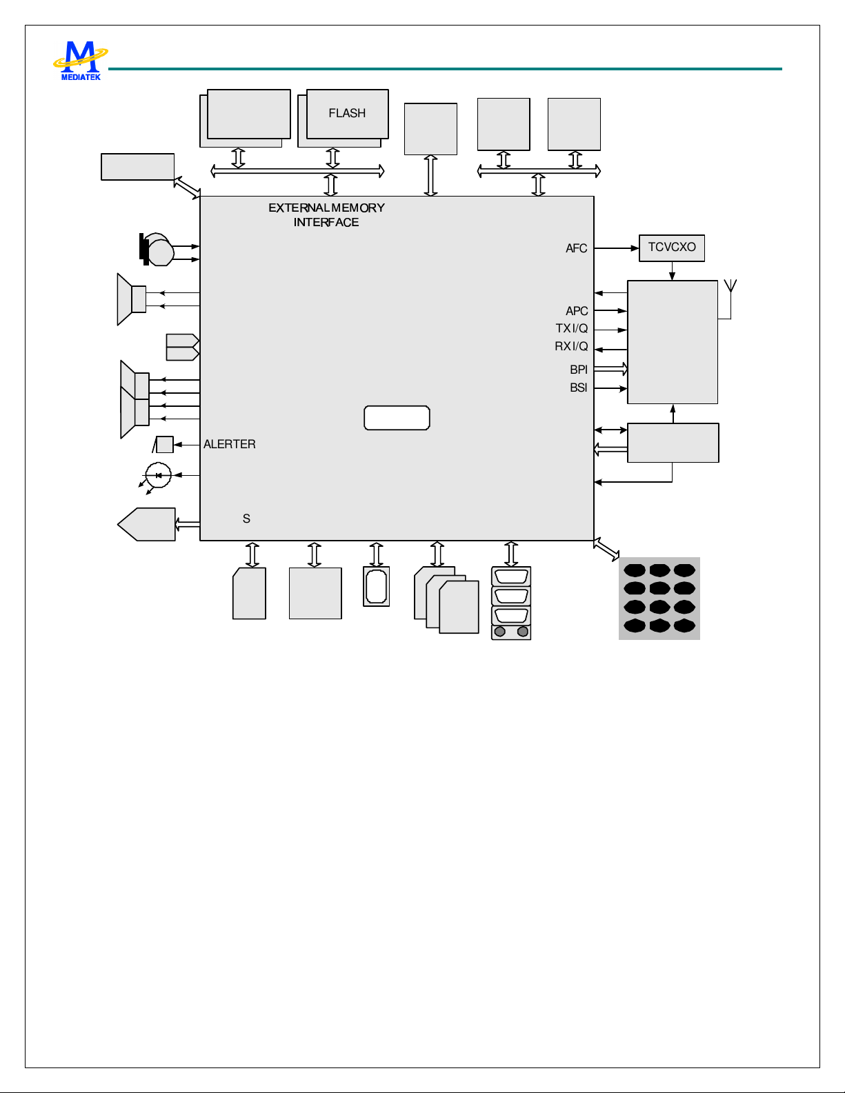
Typical application is shown in Figure 1.
Multi-media Subsystem
The MT6227 mu lti-media subsystem provides connection
to CMOS/CCD image sensor and supports resolution up to
2M pixels. With its advanced image signal and data
processing technology, MT6227 allows efficient
processing of image and video data. It also has built-in
JPEG CODEC and MPEG-4/H.263 CODEC, thus enabling
real-time creation and playback of h igh-quality images and
video. In addition to advanced image and video features,
MT6227 also utilizes high resolution DAC, digital audio,
and audio synthesis technology to provide superior audio
features for all future multi-media needs.
In order to provide more flexibility and bandwidth for
multi-media products, an additional 18-bit parallel
interface is incorporated. This interface enables connection
to LCD modules as well as connection to NAND flash
devices to allow fo r multi-media data storage capabilities.
User Interface
To provide complete user interface, MT6227 brings
together all the necessary peripheral blocks for
multi-media GSM/GPRS phone. The peripheral blocks
consists of the Keypad Scanner with the capability to
detect multiple key presses, SIM Controller, Alerter, Real
Time Clock, PWM, Serial LCD Controller, and General
Purpose Programmable I/Os. For connectivity and data
storage, the MT6227 supports UART, IrDA, USB 1.1
Slave and MMC/SD/MS/MS Pro. Furthermore, for la rge
amount of data transfer, high performance DMA (Direct
Memory Access) and hardware flow control are
implemented, which greatly enhances the performance and
reduces MCU processing load.
Audio Interface
Using a highly integrated mixed-signal Audio Front-End,
the MT6227 architecture allo ws for easy audio interfacing
with direct connection to the audio transducers. The audio
interface integrates D/A and A/D Converters for Voice
band, as well as high resolution Stereo D/A Converters for
Audio band. In addition, MT6227 also provides Stereo
Input and Analog Mux.
MT6227 supports AMR codec to adaptively optimize
speech and audio quality. Moreover, aacPlus codec is
implemented to deliver CD-quality audio at low bit rates.
External Me mory Interface
Providing the greatest capacity for expansion, MT6227
supports up to 8 state-of-the-art devices through its 16-b it
host interface. Devices such as burst/page mode Flash,
page mode SRAM, Pseudo SRAM, Color/Parallel LCD,
and multi-media co mpanion chip are all supported through
this interface. To minimize power consumption and ensure
low noise, this interface is designed for flexible I/O voltage
and allows lowering of supply voltage down to 1.8V. The
driving strength is configurable for signal integrity
adjustment. The data bus also employs retention
technology to prevent the bus from floating during turn
over.
4/32 MediaTek Inc. Confidential
Overall, MT6227’s audio features provide a rich platform
for mu lti-media applications.
Radio Interface
MT6227 integrates a mixed-signal Baseband front-end in
order to provide a well-organized radio interface with
flexibility for efficient customization. It contains gain and
offset calibration mechanisms, and filters with
programmable coefficients for comprehensive
compatibility control on RF modules. This approach also
allows the usage of a high resolution D/A Converter for
controlling VCXO or crystal, thus reducing the need for
expensive TCVCXO. MT6227 achieves great MODEM
performance by utilizing 14-bit high resolution A/D
Page 5

MT6227 GSM/GP RS Baseband Processor Technical Brief Revision 1.00
Converter in the RF downlink path. Fu rthermore, to reduce
the need for extra exte rnal current-driv ing component, the
driving strength of some BPI outputs is designed to be
configurable.
Debug Function
The JTAG interface enables in-circuit debugging of
software program with the ARM 7EJ-S core. With this
standardized debugging interface, the MT6227 provides
developers with a wide set of options in choosing ARM
development kits from different third party vendors.
Power Management
The MT6227 offers various low-power features to help
reduce system power consumption. These features include
Pause Mode of 32KHz clocking at Standby State, Power
Down Mode for individual peripherals, and Processor
Sleep Mode. In addition, MT6227 is also fabricated in
advanced low leakage CMOS process, hence providing an
overall u ltra low leakage solution.
Package
The MT6227 device is offered in a 13mm×13mm, 296-ball,
0.65 mm pitch, TFBGA package.
5/32 MediaTek Inc. Confidential
Page 6
MT6227 GSM/GP RS Baseband Processor Technical Brief Revision 1.00
DEBUGGER
AUDIO
DAC
SRAM
PSRAM
JTAG
SPEECH/AUDIO
INPUT
SPEECH/AUDIO
OUTPUT
FM STEREO
RADIO INPUT
HIFI STEREO
OUTPUT
ALERTER
PWM
SIM
I2S
USIM
FLASH
SERIAL
LCD
IMAGE
SENSOR
IMAGE INPUT
MT6227
CHIP UID
MMC/SD/MS
USB
MSPRO
NAND
FLASH
LCD
18-BIT PARALLEL
INTERFACE
SYS CLK
TX I/Q
RX I/Q
B2PSI
AUXADC
SUPPLY
VOLTAGES
UART
IRDA
KEYPAD
AFC
APC
BPI
BSI
TCVCXO
RF
MODULE
POWER
MANAGEMENT
CIRCUITRY
Figure 1 Typical application of MT6227
SERIAL
LCD
1 2 3
4 5 6
7 8 9
0 #
*
6/32 MediaTek Inc. Confidential
Page 7

MT6227 GSM/GP RS Baseband Processor Technical Brief Revision 1.00
1.1 Platform Feature
General
Integrated voice-band, audio-band and base-band
analog front ends
TFBGA 13mm×13mm, 296-ball, 0.65 mm pitch
package
MCU Subsystem
ARM7EJ-S 32-bit RISC processor
High performance multi-layer AMBA bus
Java hardware acceleration for fast Java-based
games and applets
Operating frequency: 26/52 MHz
Dedicated DMA bus
14 DMA channels
284K Bytes zero-wait-state on-chip SRAM
On-chip boot ROM for Factory Flash
Programming
Flexible I/O voltage of 1.8V ~ 2.8V for memory
interface
Configurable driving strength for memo ry
interface
User In terfaces
6-row × 7-column keypad controller with
hardware scanner
Supports mu ltiple key presses for gaming
SIM/USIM Controller with hardware T=0/T=1
protocol control
3 UARTs with hardware flow control and speed up
to 921600 bps
IrDA modulator/demodulator with hardware
framer supports SIR mode of operation
Real Time Clock (RTC) operating with a separate
power supply
General Purpose I/Os (GPIOs)
Watchdog timer for system crash recovery
2 sets of General Purpose Timer
Circuit Switch Data coprocessor
Div ision coprocessor
External Me mory Inter face
Supports up to 8 external devices
Supports 8-bit or 16-bit me mory components with
maximum size of up to 64M Bytes each
Supports Flash and SRAM with Page Mode or
Burst Mode
Supports Pseudo SRAM
Industry standard Parallel LCD Interface
Supports multi-media companion chips with 8/16
bits data width
2 Sets of Pulse Width Modulation (PWM) Output
Alerter Output with Enhanced PWM or PDM
4~10 external interrupt lines
Connecti vity
Full-speed USB 1.1 Device controller
Multi Media Card/Secure Digital Memory
Card/Memory Stick/Me mory Stick Pro host
controller
Security
Supports security key for code protection
56-bit unique chip ID
Power Management
Power Down Mode for analog and digital circuits
Processor Sleep Mode
7/32 MediaTek Inc. Confidential
Page 8

MT6227 GSM/GP RS Baseband Processor Technical Brief Revision 1.00
Pause Mode of 32KHz clocking at Standby State
7-channel Auxiliary 10-bit A/D Converter for
charger and battery monitoring and photo sensing
Test and Debug
Built-in digital and analog loop back modes for
both Audio and Baseband Front-End
DAI port co mplying with GSM Rec.11.10
JTAG port for debugging embedded MCU
8/32 MediaTek Inc. Confidential
Page 9

MT6227 GSM/GP RS Baseband Processor Technical Brief Revision 1.00
1.2 MODEM Features
Radi o Interface and B ase band Fron t End
GMSK modulator with analog I and Q channel
outputs
10-bit D/A Converter for uplink baseband I and Q
signals
14-bit high resolution A/D Converter for downlink
baseband I and Q signals
Calibration mechanism of offset and gain
mismatch for baseband A/D Converter and D/A
Converter
10-bit D/A Converter for Automatic Power
Control
13-bit high resolution D/A Converter for
Automatic Frequency Control
Programmable Radio RX filter
2 Channels bi-directional Baseband Serial
Interface (BSI) with 3-wire or 4-wire control
GSM channel coding, equalization and A5/1 and
A5/2 ciphering
GPRS GEA 1 and GEA 2 c iphering
Programmab le GSM/ GPRS Modem
Packet Switched Data with CS1/CS2/CS3/CS4
coding schemes
GSM Circuit Switch Data
GPRS Class 12
Voice Interface an d Voice Front End
Two microphone inputs sharing one low noise
amplifier with programmable gain and automatic
gain control (AGC) mechanis m
Voice power amp lifier with programmable gain
nd
2
D/A Converter for voice downlin k path
order Sig ma-Delta A/D Converter for voice
uplink path
10-Pin Baseband Parallel Interface (BPI) with
programmab le driving strength
Multi-band support
Voice and Modem CODEC
Dial tone generation
Voice Me mo
Noise Reduction
Echo Suppression / Echo Cancellation
Advanced Sidetone Oscillat ion Reduction
Digital sidetone generator with programmable
gain
Two programmable acoustic compensation filters
GSM/GPRS quad vocoders for adaptive multirate
(AMR), enhanced full rate (EFR), full rate (FR)
and half rate (HR)
Supports half-duplex hands-free operation
Compliant with GSM 03.50
FR erro r concealment
9/32 MediaTek Inc. Confidential
Page 10

MT6227 GSM/GP RS Baseband Processor Technical Brief Revision 1.00
1.3 Multi-Media Features
LCD/ NAND Flash Inter face
18-bit Parallel Interface supports 8/16 bit NAND
flash and 8/9/16/18 b it Parallel LCD
8/16 bit NAND Flash Controller with 1 -bit ECC
correction for mass storages
2 Chip selects available for high-density NAND
flash device
Serial LCD Interface with 8/9 bit format support
LCD Con troller
Hardware accelerated display
Supports simultaneous connection to up to 2
parallel LCD and 1 serial LCD modules
Supports format: RGB332, RGB444, RGB565,
RGB666, RGB888
Supports LCD panel maximum resolution up to
800x600 at 16bpp
Automatic Exposure Control
Automatic focus control
Automatic White Balance Control
Edge Enhancement Support
Flexible I/O voltage of 1.8V ~ 2.8V
JPEG Decoder
ISO/IEC 10918-1 JPEG Baseline and Progressive
modes
Supports all possible YUV fo rmats, including
grayscale format
Supports all DC/AC Huffman table parsing
Supports all quantization table parsing
Supports restart interval
Supports SOS, DHT, DQT and DRI marker
parsing
Supports hardware display rotation
Capable of combining display memories with up to
4 blending layers
Accelerated Gamma correction with
programmable gamma table.
Image Signal Processor
8/10 bit Bayer format image input
YUV422 format image input
Capable of processing image of size up to 2M
pixels
Lens shading compensation
Defect pixel correction
Synchronous flash light control
Optical black correction
Color Correction Matrix
IEEE Std 1180-1990 IDCT Standard Co mpliant
Supports progressive image processing to
minimize storage space requirement
Supports reload-able DMA for VLD stream
JPEG Enc oder
ISO/IEC 10918-1 JPEG baseline mode
ISO/IEC 10918-2 Compliance
Supports YUV422 and grayscale formats
Standard DC and AC Huffman tables
Provides 14 levels of encode quality
Image Data Processing
High throughput hardware scalar capable of
tailoring image to arbitrary size
Horizontal scaling in averaging method
Vertical scaling in bilinear method
Gamma Co rrection
10/32 MediaTek Inc. Confidential
Page 11

MT6227 GSM/GP RS Baseband Processor Technical Brief Revision 1.00
Simu ltaneous scaling for MPEG-4 encode and
LCD display
YUV and RGB color space conversion
Pixel format transform
Boundary padding
Accelerated Pixel-based luminance/chrominance
processing: hue/saturation/intensity/color
adjustment, Gamma correction and
grayscale/invert/sepia-tone effects
Accelerated Programmable Spatial Filtering :
Linear filter, Non-linear filter and Multi-pass
artistic effects
Hardware accele rated image editing
MPEG-4/ H.263 CODEC
Hardware Video CODEC
ISO/IEC 14496-2 simple profile:
decode @ level 0/1/2/3
encode @ level 0
Supported visual tools for decoder: I-VOP, P -VOP,
AC/DC prediction, 4-MV, Unrestricted M V, Error
Resilience, Short Header
Error Resilience for decoder: Slice
Resynchronization, Data Partitioning, Reversible
VLC
Supported visual tools for encoder: I-VOP, P -VOP,
Half-pel, DC prediction, Unrestricted MV,
Reversible VLC, Short Header
BitBlt: multi-BitBlt without transform, 7 rotate,
mirror (transparent) BitBlt
Alpha blending
Line drawing: normal line, dotted line
Font caching: normal font, Italic font
Supports 16-bpp RGB565 and 8-bpp index color
modes with one color palette inside
Command queue with 32 levels
Audio CODEC
Wavetable synthesis with up to 64 tones
Advanced wavetable synthesizer capable of
generating simulated stereo
Wavetable including GM full set of 128
instruments and 47 sets of percussions
PCM Playback and Record
Digital Audio Playback
aacPlus decode support
Audio Inter face an d Audio Front End
Supports I2S interface
High resolution D/A Converters for Stereo Audio
playback
Stereo analog input for stereo audio source
Analog multiplexer for Stereo Audio
Stereo to Mono Conversion
FM radio recording
Supports encoding motion vector of range up
to –64/+63.5 pixels
ITU-T H.263 profile 0 @ level 10
AAC/HE-AAC/AMR audio decode support
AMR audio encode support
2D Accelerator
Rectangle fill
11/32 MediaTek Inc. Confidential
Page 12

MT6227 GSM/GP RS Baseband Processor Technical Brief Revision 1.00
1.4 General Description
Figure 2 details the block diagram of MT6227. Based on a dual-processor architecture, MT6227 integrates both an
ARM7EJ-S core and a digital signal processor core. ARM 7EJ-S is the main processor that is responsible for running
high-level GSM/GPRS protocol software as well as multi-media applications. The digital signal processor handles the
low-level MODEM as well as advanced audio functions. Except for some mixed-signal circuitries, the other building
blocks in MT6227 are connected to either the microcontroller or the digital signal processor.
Specifically, MT6227 consists of the following subsystems:
Microcontroller Un it (MCU) Subsystem - includes an ARM7EJ-S RISC processor and its accompanying memory
management and interrupt handling logics.
Digital Signal Processor (DSP) Subsystem - includes a DSP and its accompanying memory, memo ry controlle r,
and interrupt controller.
MCU/DSP Interface - where the MCU and the DSP exchange hardware and software informat ion.
Microcontroller Peripherals - includes all user interface modules and RF control interface modules.
Microcontroller Coprocessors - runs computing-intensive processes in place of Microcontroller.
DSP Peripherals - hardware accelerators for GSM/GPRS channel codec.
Multi-media Subsystem - integrates several advanced accelerators to support multi-media applications.
Voice Front End - the data path for converting analog speech fro m and to digital speech.
Audio Front End - the data path for converting stereo audio from stereo audio source
Baseband Front End - the data path for converting digital signal from and to analog signal of RF modules.
Timing Generator - generates the control signals related to the TDMA frame timing.
Power, Reset and Clock subsystem - manages the power, reset, and clock distribution inside MT6227.
Details of the individual subsystems and blocks are described in following Chapters.
12/32 MediaTek Inc. Confidential
Page 13

MT6227 GSM/GP RS Baseband Processor Technical Brief Revision 1.00
MIC-0
MIC-1
VOICE
AUDI O-L
AUDI O-R
STEREO-L
STEREO-R
RX-I
RX-Q
TX-I
TX-Q
AUX
ADC
AFC
ADC
ADC
DAC
DAC
ADC
DAC AFC
+
+
BASEBAND
PATH
AUX
ADC
ADC
DAC
DAC
DAC
AUDIO
PATH
BRIDGE
INTERRUPT
CONTROL
2D
ENGINE
PATCH
UNIT
MCU/DSP
INTE RFACE
ARM7EJ-S
MEMO RY
DSP
BOOT
ROM
ON-CHIP
GRAPHIC MEMORY
CONTROLLER
TRAP
UNIT
DMA
CONTROL
S RA M
INTERRUPT
CONTROL
DSP COPROCES
SOR
DSP COPROCES
SOR
DSP COPROCES
SOR
USB
EXTERNAL
MEMO RY
INTERFACE
LCD
CONTROLLER
NAND
FLASH
INTERFA
CE
USB
FLASH
SRAM
PSRAM
NAND
LCD
APC
SERIAL RF
CONTROL
PARALLE L
RF CONT ROL
SYSTEM
CLOCK
13/2 6MHZ
DAC APC
BSI
BPI
CLOCK
GEN
32K
OSC
32K HZ CRYSTAL
WAKE UP USE R INTE RFACERESET
Figure 2 MT6227 block diagram.
RTC
GPT
TDMA
TIMER
SIM GPIO
WDT
IMAGE
DMA
PWM
IMAGE
POST
PROC
KEYPAD
SCAN
GIF
DECO DE
IMAGE RESIZER
ALERTER
SERIAL
LCD
MMC
SD/MS
MS PRO
CO NNECTIVITYSERIAL PORT
MPEG-4
VIDEO
CODEC
JPEG
CODE C
B2PSI IRDA
UART
IMAGE
SIGNAL
PROC
I2C
MT6227
IMAGE
SENSO R
IMAGE
SENSO R
13/32 MediaTek Inc. Confidential
Page 14

MT6227 GSM/GP RS Baseband Processor Technical Brief Revision 1.00
2 Product Description
2.1 Pin Outs
One type of package for this product, TFBGA 13mm*13mm, 296-ball, 0.65 mm pitch Package, is offered.
Pin outs and the top view are illustrated in Figure 3 for this package. Outline and dimension of package is illustrated in
Figure 4, while the definition of package is shown in Table 1.
14/32 MediaTek Inc. Confidential
Page 15

MT6227 GSM/GP RS Baseband Processor Technical Brief Revision 1.00
14131211106321 87 954
AVDD_
RFE
APC
AVSS_
RFE
AVDD_
GSMR
FTX
BUPAI
N
BUPAI
P
BUPA
QN
BUPA
QP
AV SS_
GSMR
FTX
CMDA
T9
CMDA
T8
CMDA
T7
CMDA
T6
SYSCL
NC GPIO8GPIO9
A
XOUT
B
BBWA
C
KEUP
VDDK
D
JTMS
E
VDD33
F
BPI_ B
G
US6
BSI_ C
H
S0
J
VDD33
K
L
K
AVDD_
RTC
XIN
VSS33
BPI_ B
US1
BPI_ B
US5
VSS33
LSA0
LPCE1
#
NC
AVDD_
PLL
AVSS_
PLL
TESTM
ODE
JTCKJTDI
BPI_ B
US0
BPI_ B
US4
BPI_ B
US9
LSCKLSDA
LSCE1
#
LRD#LPA0LWR#
AFC_B
YP
AFC
AUX_R
EF
NC
JTRST
#
BPI_B
US3
BPI_B
US8
BSI_C
LK
LSCE0
#
LRST#
AUXA
DIN3
DIN6
AUXA
AUXA
DIN2
DIN5
AUXA
AUXA
DIN1
DIN4
AUXA
PL L_O
DIN0
UT
IBOOT
NC NC NC
JTDOJRTCK
NLD17
BPI_ B
NLD16
US2
BPI_ B
US7
BSI_ D
ATA
NC
LPCE0
#
AUXA
AU_VI
BDLAI
N1_P
N
BDLAI
AU_VI
P
N1_N
BDLA
AU_VI
QN
N0_N
AU_VI
BDLA
N0_P
QP
AVSS_
AGND
AFE
_RFE
CMMC
CMPC
LK
LK
NLD8 NLD9 NLD10
NLD11 NLD12
NLD13 NLD14 NLD15
AU_O
AGND
UT0_P
_AFE
AU_O
AU_VR
UT0_N
EF_P
AU_MI
AU_VR
CBIAS
EF_N
_P
AU_MI
AVDD_
CBIAS
AFE
_N
VDDK VSS33
CMHREFCMVR
EF
CMRS
CMPD
CMDA
T0
AU_F
AVSS _
BUF
AVDD_
BUF
AU_M_
BYPR
AU_R
BIAS
T
N
MINR
AU_F
MINL
AU_M_
BYPL
AVSS_
MBUF
VSS33
_IS
AU_M
OUTR
AU_M
OUTL
AVDD_
MBUF
NC
VDD33
_IS
IRDA_
TXD
NC
SIMVC
C
GPIO2
VSS33
VSS33
GPIO7
GPIO4
DAICL
K
KROW
3
KCOL1KCOL2KCOL3
IRDA_
RXD
URT S1UCTS1
SIMDA
TA
SIMCL
K
GPIO6
DAIR STDAIPC
DAIP C
MOUT
KROW
2
KCOL 0
KCOL 5KCOL6
URXD2
URXD1
SIMRS
T
_IS
VDDK
KROW
1
KROW
4
IRDA_
PDN
UTXD3URXD3 VSS33
SIMSE
L
GPIO3
1918171615
GPIO5
DAISY
NC
MIN
KROW
0
VDD33
KROW
5
KCOL4
VDDK
UTXD2
UTXD1
VDD33
A
B
C
D
E
F
G
H
J
K
L
NLD6
NLD3
NLD7NLD5VDDK
NLD4NLD2NLD1
M
N
VSS33
NLD0
CMDA
T5
T4
MT6227
CMDAT3CMDA
CMDA
CMDA
T1
T2
TFBGA
NRE#
P
R
SRCL
T
KENA
SYSRS
U
T#
EINT0
V
EINT2
W
Figure 3 Top View of MT6227 TFBGA 13mm*13mm, 296-ball, 0.65 mm pitch Pac kage
NALENWE# NRNBNCLE
PWM1VDD33 MIRQ
SRCL
SRCL
KENA
KE NAI
GPIO0
EINT1
VSS33
EINT3
_EMI
EA25 EA24
N
NCE#PWM2
ALERT
ER
EA23
EA22 EA13
VDD33
_EMI
EA14 MFIQ
EA10 EA7
EA16
VSS33
_EMI
EA17
EA11 EA8
EA12
VDD33
EA18 EA15
EA19
EA20
EA21
_EMI
VSS33
_EMI
VDDK
EA9
Top-View
EA0
NC
EA4
EA1
EA2EA5
VSS33
EA6
_EMI
VDD33
EA3
_EMI
EWAIT
EPDN#
EADV#
ECLK
VDD33
_EMI
ELB#
ECS0#
ECS4#
ECS5# ECS1#
ECS6#
VSS33
_EMI
ECS7#
EUB# ED13
ECS2#
ERD#
VSS33
ECS3# VDDK
_EMI
VDD33
EWR#
_EMI
14131211106321 87 954 1918171615
VDD33
_MC
MCDA
0
VDD33
_USB
ED1 ED0
ED14
ED15
VDD33
_EMI
MCDA
1
USB_D
P
ED11
VSS33
_EMI
ED12
MCCK
MCDA2MCDA
USB_D
VSS33
M
_MC
WATC
HDOG
VDD33
ED3
_EMI
ED5
ED8
ED6
ED9
VDD33
ED10
_EMI
RON
0
_EMI
ED2
ED4
_EMI
ED7
M
N
P
R
T
U
V
W
GPIO1MCINSM CWP
MCPW
3
MCCM
VSS33
VSS33
15/32 MediaTek Inc. Confidential
Page 16

MT6227 GSM/GP RS Baseband Processor Technical Brief Revision 1.00
$%$$$*$)
$% & ' $( ) * $$$$'$&
#
"
!
,
/
.
"
-
$
+
Figure 4 Outlines and Dimension of TFBGA 13mm*13mm, 296-ball, 0.65 mm pitch Package
Body Size Ball Count Ball Pitch Ball Dia. Package Thk. Stand O ff Substrate Thk.
D E N e b A (Max.) A1 C
13 13 296 0.65 0.3 1.2 0.21 0.36
Table 1 Definition of TFBGA 13mm*13mm, 296-ball, 0.65 mm pitch Package (Unit: mm)
16/32 MediaTek Inc. Confidential
Page 17

MT6227 GSM/GP RS Baseband Processor Technical Brief Revision 1.00
2.2 Top Marking Definition
MT6227A: Part No.
DDDD: Date Code
###: Subcontractor Code
M T 6 22 7 A
D D D D- # ##
L L L LL
LLLLL: Lot No.
S: Special Code
S
17/32 MediaTek Inc. Confidential
Page 18

MT6227 GSM/GP RS Baseband Processor Technical Brief Revision 1.00
2.3 Pin Description
Ball
13X13
JTAG Port
E4 JTRST# I JTAG test port reset input PD Input
E3 JTCK I JTAG test port clock input PU Input
E2 JTDI I JTAG test port data input PU Input
E1 JTMS I JTAG test port mode switch PU Input
F5 JTDO O JTAG test port data output 0
F4 JRTCK O JTAG test port returned clock output 0
RF Parallel Control Unit
F3 BPI_BUS0 O RF hard-wire control bus 0 0
F2 BPI_BUS1 O RF hard-wire control bus 1 0
G5 BPI_B US2 O RF hard-wire control bus 2 0
G4 BPI_B US3 O RF hard-wire control bus 3 0
G3 BPI_B US4 O RF hard-wire control bus 4 0
G2 BPI_B US5 O RF hard-wire control bus 5 0
G1 BPI_BUS6 IO RF hard-wire control bus 6 GPIO10 BPI_BUS6 PD Input
H5 BPI_BUS7 IO RF hard-wire control bus 7 GPIO11 BPI_BUS7 65MHz 26MHz PD Input
H4 BPI_BUS8 IO RF hard-wire control bus 8 GPIO12 BPI_BUS8 13MHz 32KHz PD Input
H3 BPI_BUS9 IO RF hard-wire control bus 9 GPIO13 BPI_BUS9 BSI_CS1 PD Input
RF Serial Control Unit
H1 BSI_CS0 O RF 3-wire interface chip select 0 0
J5 BSI_DATA O RF 3-wire interface data output 0
J4 BSI_CLK O RF 3-wire interface clock output 0
PWM Interface
R3 PWM1 IO Pulse width modulated signal 1 GPIO21 PWM1 DSP_GPO0 TBTXFS PD Input
R2 PWM2 IO Pulse width modulated signal 2 GPIO22 PWM2 DSP_GPO1 TBRXEN PD Input
T4 ALERTER IO Pulse width modulated signal for buzzer GPIO23 ALERTER DSP_GPO2 BTRXFS PD Input
Serial LCD/PM IC Interface
J3 LSCK IO Serial display interface data output GPIO16 LSCK TDMA_CK TBTXEN PU Input
J2 LSA0 IO Serial display interface address output GPIO17 LSA0 TDMA_D1 TDTIRQ PU Input
J1 LSDA IO Serial display interface clock output GPIO18 LSDA TDMA_D0 TCTIRQ2 PU Input
K4 LSCE0# IO Serial display interface chip select 0
K3 LSCE1# IO Serial display interface chip select 1
Parallel LCD/Nand-Flash Interface
K2 LPCE1# IO Parallel display interface chip select 1
L5 LPCE0# O Parallel display interface chip select 0
L4 LRST# O Parallel display interface Reset Signal 1
L3 LRD# O Parallel display interface Read Strobe 1
L2 LPA0 O Parallel display interface address output 1
L1 LWR# O Parallel display interface Write Strobe 1
F6 NLD17 IO Parallel LCD/Nand-Flash Data 17 GPIO56 NLD17 MCDA7 DSP_TID0
Name Dir Description
output
output
output
output
Mode0 Mode1 Mode2 Mode3
GPIO19 LSCE0# TDMA_FS TCTIRQ1 PU Input
GPIO20 LSCE1# LPCE2# TEVTVAL PU Input
GPIO24 LPCE1# NCE1# MCU_TID0 PU Input
1
PU/
Rese
PD
t
PD Input
18/32 MediaTek Inc. Confidential
Page 19

MT6227 GSM/GP RS Baseband Processor Technical Brief Revision 1.00
G6 NLD16 IO Parallel LCD/Nand-Flash Data 16 GPIO55 NLD16 MCDA6 PD Input
L11 NLD15 IO Parallel LCD/Nand-Flash Data 15 PD Input
L10 NLD14 IO Parallel LCD/Nand-Flash Data 14 PD Input
L9 NLD13 IO Parallel LCD/Nand-Flash Data 13 PD Input
K11 NLD12 IO Parallel LCD/Nand-Flash Data 12 PD Input
K9 NLD11 IO Parallel LCD/Nand-Flash Data 11 PD Input
J11 NLD10 IO Parallel LCD/Nand-Flash Data 10 PD Input
J10 NLD9 IO Parallel LCD/Nand-Flash Data 9 PD Input
J9 NLD8 IO Parallel LCD/Nand-Flash Data 8 PD Input
M5 NLD7 IO Parallel LCD/Nand-Flash Data 7 PD Input
M4 NLD6 IO Parallel LCD/Nand-Flash Data 6 PD Input
M3 NLD5 IO Parallel LCD/Nand-Flash Data 5 PD Input
N5 NLD4 IO Parallel LCD/Nand-Flash Data 4 PD Input
N4 NLD3 IO Parallel LCD/Nand-Flash Data 3 PD Input
N3 NLD2 IO Parallel LCD/Nand-Flash Data 2 PD Input
N2 NLD1 IO Parallel LCD/Nand-Flash Data 1 PD Input
N1 NLD0 IO Parallel LCD/Nand-Flash Data 0 PD Input
P5 NRNB IO Nand-Flash Read/Busy Flag GPIO25 NRNB DSP_TID1 MCU_TID1 PU Input
P4 NCLE IO Nand-Flash Command Latch Signal GPIO26 NCLE DSP_TID2 MCU_TID2 PD Input
P3 NALE IO Nand-Flash Address Latch Signal GPIO27 NALE DSP_TID3 MCU_TID3 PD Input
P2 NWE# IO Nand-Flash Write Strobe GPIO28 NWE# DSP_TID4 MCU_DID
P1 NRE# IO Nand-Flash Read Strobe GPIO29 NRE# DSP_TID5 MCU_DFS PU Input
R4 NCE# IO Nand-Flash Chip select output GPIO30 NCE# DSP_TID6 MCU_DCK PU Input
SIM Card Interface
L18 SIMRST O SIM card reset output 0
L17 SIMCLK O SIM card clock output 0
K15 SIMVCC O SIM card supply power control 0
K16 SIMSEL IO SIM card supply power select GPIO32 SIMSEL PD Input
K17 SIMDATA IO SIM card data input/output 0
Dedicated GPIO Interface
U2 GPIO0 IO General purpose input/output 0 GPIO0 DICK DSP_GPO3 PD Input
M19 GPIO1 IO General purpose input/output 1 GPIO1 BSI_RFIN PD Input
L15 GPIO2 IO General purpose input/output 2 GPIO2 DID PD Input
L16 GPIO3 IO General purpose input/output 3 GPIO3 DIMS PD Input
C17 GPIO4 IO General purpose input/output 4 GPIO4 DSP_CLK DSPLCK EDICK PD Input
A19 GPIO5 IO General purpose input/output 5 GPIO5 AHB_CLK DSPLD3 EDIWS PD Input
B18 GPIO6 IO General purpose input/output 6 GPIO6 ARM_CLK DSPLD2 CMFLASH PD Input
PU Input
B17 GPIO7 IO General purpose input/output 7 GPIO7 SLOW_CK DSPLD1 EDIDAT PD Input
A18 GPIO8 IO General purpose input/output 19 GPIO8 SCL DSPLD0 PD Input
A17 GPIO9 IO General purpose input/output 21 GPIO9 SDA DSPLSYNC PD Input
Miscellaneous
U1 SYSRST# I System reset input active low Input
R18 WATCHDOG O Watchdog reset output 1
19/32 MediaTek Inc. Confidential
Page 20

MT6227 GSM/GP RS Baseband Processor Technical Brief Revision 1.00
#
T3 SRCLKENAN O External TCXO enable output active
low
T1 SRCLKENA O External TCXO enable output active
high
T2 SRCLKEN AI IO External TCXO enable input GPIO31 SRCLKEN
E5 IBOOT I Boot Device Configuration Input PD Input
Keypad Interface
G17 KCOL6 I Keypad column 6 PU Input
G18 KCOL5 I Keypad column 5 PU Input
G19 KCOL4 I Keypad column 4 PU Input
F15 KCOL3 I Keypad column 3 PU Input
F16 KCOL2 I Keypad column 2 PU Input
F17 KCOL1 I Keypad column 1 PU Input
F18 KCOL0 I Keypad column 0 PU Input
F19 KROW5 O Keypad row 5 0
E16 KROW4 O Keypad row 4 0
E17 KROW3 O Keypad row 3 0
E18 KROW2 O Keypad row 2 0
D16 KROW1 O Keypad row 1 0
D19 KROW0 O Keypad row 0 0
External Interrupt Interface
V1 EINT0 I External interrupt 0 PU Input
U3 EINT1 I External interrupt 1 PU Input
W1 EINT2 I External interrupt 2 PU Input
V2 EINT3 I External interrupt 3 PU Input
R5 MIRQ IO Interrupt to MCU GPIO41 MIRQ 13MHz 32KHz PU Input
R17 MFIQ IO Interrupt to MCU GPIO42 MFIQ PU Input
External Memory Interface
R16 ED0 IO External memory data bus 0 Input
R15 ED1 IO External memory data bus 1 Input
T19 ED2 IO External memory data bus 2 Input
T17 ED3 IO External memory data bus 3 Input
U19 ED4 IO External memory data bus 4 Input
U18 ED5 IO External memory data bus 5 Input
V18 ED6 IO External memory data bus 6 Input
W19 ED7 IO External memory data bus 7 Input
U17 ED8 IO External memory data bus 8 Input
V17 ED9 IO External memory data bus 9 Input
W17 ED10 IO External memory data bus 10 Input
T16 ED11 IO External memory data bus 11 Input
W16 ED12 IO External memory data bus 12 Input
T15 ED13 IO External memory data bus 13 Input
U15 ED14 IO External memory data bus 14 Input
V15 ED15 IO External memory data bus 15 Input
U14 ERD# O External memory read strobe 1
W14 EWR# O External memory write strobe 1
R13 ECS0# O External memory chip select 0 1
GPO1 SRCLKEN
AN
GPO0 SRCLKENA 1
AI
0
PD Input
20/32 MediaTek Inc. Confidential
Page 21

MT6227 GSM/GP RS Baseband Processor Technical Brief Revision 1.00
T13 ECS1# O External memory chip select 1 1
U13 ECS2# O External memory chip select 2 1
V13 ECS3# O External memory chip select 3 1
R12 ECS4# IO External memory chip select 4 GPIO54 ECS4# PU 1
T12 ECS5# IO External memory chip select 5 GPIO53 ECS5# PU 1
U12 ECS6# IO External memory chip select 6 GPIO52 ECS6# PU 1
W12 ECS7# IO External memory chip select 7 GPIO40 ECS7# PU 1
R14 ELB# O External memory lower byte strobe 1
T14 EUB# O External memory upper byte strobe 1
T11 EPDN# O Power Down Control Signal for
PSRAM
U11 EADV# O Address valid for burst mode flash
memory
R11 EWAIT I External device wait signal Input
V11 ECLK O Clock for flash memory 0
R10 EA0 O External memory address bus 0 0
T10 EA1 O External memory address bus 1 0
U10 EA2 O External memory address bus 2 0
W10 EA3 O External memory address bus 3 0
T9 EA4 O External memory address bus 4 0
U9 EA5 O External memory address bus 5 0
V9 EA6 O External memory address bus 6 0
R8 EA7 O External memory address bus 7 0
T8 EA8 O External memory address bus 8 0
W8 EA9 O External memory address bus 9 0
R7 EA10 O External memory address bus 10 0
T7 EA11 O External memory address bus 11 0
U7 EA12 O External memory address bus 12 0
V7 EA13 O External memory address bus 13 0
R6 EA14 O External memory address bus 14 0
T6 EA15 O External memory address bus 15 0
U6 EA16 O External memory address bus 16 0
W6 EA17 O External memory address bus 17 0
T5 EA18 O External memory address bus 18 0
U5 EA19 O External memory address bus 19 0
V5 EA20 O External memory address bus 20 0
W5 EA21 O External memory address bus 21 0
V4 EA22 O External memory address bus 22 0
U4 EA23 O External memory address bus 23 0
W3 EA24 O External memory address bus 24 GPO3 EA24 0
W2 EA25 O External memory address bus 25 GPO4 EA25 13MHz 32KHz 0
USB Interface
P16 USB_DP IO USB D+ Input/Output
P17 USB_DM IO USB D- Input/Output
Memory Card Interface
P19 MCCM0 IO SD Command/MS Bus State Output
N15 MCDA0 IO SD Serial Data IO 0/MS Serial Data IO
N16 MCDA1 IO SD Serial Data IO 1
N17 MCDA2 IO SD Serial Data IO 2
GPO2 EPDN# 6.5MHz 26MHz 0
1
21/32 MediaTek Inc. Confidential
Page 22

MT6227 GSM/GP RS Baseband Processor Technical Brief Revision 1.00
N18 MCDA3 IO SD Serial Data IO 3
M18 MCCK O SD Serial Clock/MS Serial Clock
Output
N19 MCPWRON O SD Power On Control Output
M16 MCWP IO SD Write Protect Input GPIO15 MCWP PU
M17 MCINS IO SD Card Detect Input GPIO14 MCINS PU
UART Interface
K18 URXD1 I UART 1 receive data PU Input
K19 UTXD1 O UART 1 transmit data 1
J16 UCTS1 I UART 1 clear to send PU Input
J17 URTS1 O UART 1 request to send 1
J18 URXD2 IO UART 2 receive data GPIO35 URXD2 UCTS3 EINT6 PU Input
J19 UTXD2 IO UART 2 transmit data GPIO36 UTXD2 URTS3 EINT4 PU Input
H15 URXD3 IO UART 3 receive data GPIO33 URXD3 EINT7 PU Input
H16 UTXD3 IO UART 3 transmit data GPIO34 UTXD3 EINT5 PU Input
H17 IRDA_RXD IO IrDA receive data GPIO37 IRDA_RXD UCTS2 PU Input
G15 IRDA_TXD IO IrDA transmit data GPIO38 IRDA_TXD URTS2 PU Input
G16 IRDA_PDN IO IrDA Power Down Control GPIO39 IRDA_PDN PU Input
Digital Audio Interface
D17 DAICLK IO DAI clock output GPIO43 DAICLK DSPLD7 PU Input
D18 DAIPCMOUT IO DAI pcm data out GPIO44 DAIPCMO
UT
C19 DAIPCMIN IO DAI pcm data input GPIO45 DAIPCMIN DSPLD5 PU Input
C18 DAIRST IO DAI reset signal input GPIO47 DAIRST DSPLD4 PU Input
B19 DAISYNC IO DAI frame synchronization signal
output
Image Sensor Interface
J12 CMRST IO Image sensor reset signal output GPIO48 CMRST PD Input
K12 CMPDN IO Image sensor power down control GPIO49 CMPDN PD Input
H12 CMVREF I Sensor vertical reference signal input Input
H11 CMHREF I Sensor horizontal reference signal input Input
H9 CMPCLK I Image sensor pixel clock input Input
H10 CMMCLK O Image sensor master clock output Outp
H8 CMDAT9 I Image sensor data input 9 Input
J8 CMDAT8 I Image sensor data input 8 Input
K8 CMDAT7 I Image sensor data input 7 Input
L8 CMDAT6 I Image sensor data input 6 Input
M8 CMDAT5 I Image sensor data input 5 Input
M9 CMDAT4 I Image sensor data input 4 Input
M10 CMDAT3 I Image sensor data input 3 Input
M11 CMDAT2 I Image sensor data input 2 Input
M12 CMDAT1 IO Image sensor data input 1 GPIO50 CMDAT1 MCDA5 PD Input
L12 CMDAT0 IO Image sensor data input 0 GPIO51 CMDAT0 MCDA4 PD Input
Analog Interface
B15 AU_MOUL Audio analog output left channel
GPIO46 DAISYNC BFEPRBO PU Input
DSPLD6 PD Input
ut
22/32 MediaTek Inc. Confidential
Page 23

MT6227 GSM/GP RS Baseband Processor Technical Brief Revision 1.00
A15 AU_ MOUR Audio analog output right channel
C14 AU_M_BYPL Audio DAC bypass pin
B14 AU_FMINL FM radio analog input left channel
A14 AU_FMINR FM radio analog input right channel
D13 AU_R_BIAS Audio DAC bias resistor pin
C13 AU_M_BYPR Audio DAC bypass pin
B12 AU_OUT0_N Earphone 0 amplifier output (-)
A12 AU_OUT0_P Earphone 0 amplifier output (+)
C12 AU_MICBIA
S_P
D12 AU_MICBIA
S_N
C11 AU_VREF_N Audio reference voltage (-)
B11 AU_VREF_P Audio reference voltage (+)
D10 AU_VIN0_P Microphone 0 amplifier input (+)
C10 AU_VIN0_N Microphone 0 amplifier input (-)
B10 AU_VIN1_N Microphone 1 amplifier input (-)
A10 AU_VIN1_P Microphone 1 amplifier input (+)
D9 BDLAQP Quadrature input (Q+) baseband codec
C9 BDLAQN Quadrature input (Q-) baseband codec
A9 BDLAIN In-phase input (I+) baseband codec
B9 BDLAIP In-phase input (I-) baseband codec
B8 BUPAIP In-phase output (I+) baseband codec
A8 BUPAIN In-phase output (I-) baseband codec
C8 BUPAQN Quadrature output (Q+) baseband codec
D8 BUPAQP Quadrature output (Q-) baseband codec
B7 APC Automatic power control DAC output
D6 AUXADIN0 Auxiliary ADC input 0
C6 AUXADIN1 Auxiliary ADC input 1
B6 AUXADIN2 Auxiliary ADC input 2
A6 AUXADIN3 Auxiliary ADC input 3
C5 AUXADIN4 Auxiliary ADC input 4
B5 AUXADIN5 Auxiliary ADC input 5
A5 AUXADIN6 Auxiliary ADC input 6
C4 AUX_REF Auxiliary ADC reference voltage input
B4 AFC Automatic frequency control DAC
A4 AFC_BYP Automatic frequency control DAC
VCXO Interface
A2 SYSCLK 13MHz or 26MHz system clock input
D5 PLL_OUT PLL test pin
RTC Interface
Microphone bias supply (+)
Microphone bias supply (-)
downlink
downlink
downlink
downlink
uplink
uplink
uplink
uplink
output
bypass capacitance
23/32 MediaTek Inc. Confidential
Page 24

MT6227 GSM/GP RS Baseband Processor Technical Brief Revision 1.00
C2 XIN 32.768 KHz crystal input
B1 XOUT 32.768 KHz crystal output
C1 BBWAKEUP O Baseband power on/off control 1
D3 TESTMODE I TESTMODE enable input PD Input
Supply Voltages
D1 VDDK Supply voltage of internal logic
M1 VDDK Supply voltage of internal logic
V8 VDDK Supply voltage of internal logic
E11 VDDK Supply voltage of internal logic
V16 VDDK Supply voltage of internal logic
H19 VDDK Supply voltage of internal logic
C16 VDDK Supply voltage of internal logic
W4 VDD33_EMI Supply voltage of memory interface
driver
W7 VDD33_EMI Supply voltage of memory interface
driver
W9 VDD33_EMI Supply voltage of memory interface
driver
W11 VDD33_EMI Supply voltage of memory interface
driver
W13 VDD33_EMI Supply voltage of memory interface
driver
W15 VDD33_EMI Supply voltage of memory interface
driver
W18 VDD33_EMI Supply voltage of memory interface
driver
T18 VDD33_EMI Supply voltage of memory interface
driver
V3 VSS33_EMI Ground of memory interface driver
V6 VSS33_EMI Ground of memory interface driver
U8 VSS33_EMI Ground of memory interface driver
V10 VSS33_EMI Ground of memory interface driver
V12 VSS33_EMI Ground of memory interface driver
V14 VSS33_EMI Ground of memory interface driver
U16 VSS33_EMI Ground of memory interface driver
V19 VSS33_EMI Ground of memory interface driver
R19 VSS33_EMI Ground of memory interface driver
P15 VDD33_USB Supply voltage of USB transceiver
M15 VDD33_MC Supply voltage of memory card
interface drivers
P18 VSS33_USB/
MC
E15 VDD33_IS Supply voltage of image sensor
A16 VSS33_IS Ground of image sensor interface
E14 VSS33_IS Ground of image sensor interface
F1 VDD33 Supply voltage for pad
K1 VDD33 Supply voltage for pad
R1 VDD33 Supply voltage for pad
L19 VDD33 Supply voltage for pad
E19 VDD33 Supply voltage for pad
Ground of USB/memory card interface
interface drivers
24/32 MediaTek Inc. Confidential
Page 25

MT6227 GSM/GP RS Baseband Processor Technical Brief Revision 1.00
D2 VSS33 Ground
H2 VSS33 Ground
M2 VSS33 Ground
H18 VSS33 Ground
B16 VSS33 Ground
E12 VSS33 Ground
B2 AVDD_RTC Supply voltage for Real Time Clock
Analog Supplies
B3 AVDD_PLL Supply voltage for PLL
C3 AVSS_PLL Ground for PLL supply
C15 AVDD_MBUF Supply Voltage for Audio band section
D14 AVSS_MBUF GND for Audio band section
B13 AVDD_BUF Supply voltage for voice band transmit
section
A13 AVSS_BUF GND for voice band transmit section
D11 AVDD_AFE Supply voltage for voice band receive
section
A11 AGND_AFE GND reference voltage for voice band
section
E10 AVSS_AFE GND for voice band receive section
E9 AGND_RFE GND reference voltage for baseband
section, APC, AFC and AUXADC
E8 AVSS_GSMR
FTX
D7 AVDD_GSM
RFTX
C7 AVSS_RFE GND for baseband receive section,
A7 AVDD_RFE Supply voltage for baseband receive
GND for baseband transmit section
Supply voltage for baseband transmit
section
APC, AFC and AUXADC
section, APC, AFC and AUXADC
Table 2 Pin Descriptions (Bol ded types are functions at reset)
25/32 MediaTek Inc. Confidential
Page 26

MT6227 GSM/GP RS Baseband Processor Technical Brief Revision 1.00
2.4 Power Description
Ball
13X13
A19 GPIO5
A18 GPIO6
B17 GPIO7
A18 GPIO8
A17 GPIO9
B16 VSS33
C16 VDDK Typ. 1.8V
A16 VSS33_IS
J12 CMRST
K12 CMPDN
H12 CMVREF
H11 CMHREF
H9 CMPCLK
H10 CMMCLK
H8 CMDAT9
E15 VDD33_IS Typ. 1.8~2.8V
J8 CMDAT8
K8 CMDAT7
L8 CMDAT6
M8 CMDAT5
M9 CMDAT4
M10 CMDAT3
M11 CMDAT2
M12 CMDAT1
L12 CMDAT0
E12 VSS33
E11 VDDK Typ. 1.8V
E14 VSS33_IS
C15 AVDD_MBUF Typ. 2.8V
B15 AU_MOUTL
A15 AU_MOUTR
D14 AVSS_MBUF
C14 AU_M_BYPL
C13 AU_M_BYPR
D13 AU_R_BIAS
B14 AU_FMINL
A14 AU_FMINR
B12 AU_OUT0_N
B13 AVDD_BUF Typ. 2.8V
A12 AU_OUT0_P
A13 AVSS_BUF
C12 AU_MICBIAS_P
D12 AU_MICBIAS_N
D11 AVDD_AFE Typ. 2.8V
Name IO Supply IO GND Core Supply Core GND Remark
VDD33 VSS33 VDDK VSSK
VDD33_IS VSS33_IS VDDK VSSK
VDD33_IS VSS33_IS VDDK VSSK
26/32 MediaTek Inc. Confidential
Page 27

MT6227 GSM/GP RS Baseband Processor Technical Brief Revision 1.00
C11 AU_VREF_N
B11 AU_VREF_P
A11 AGND_AFE
D10 AU_VIN0_P
C10 AU_VIN0_N
B10 AU_VIN1_N
A10 AU_VIN1_P
E10 AVSS_AFE
D9 BDLAQP
C9 BDLAQN
E9 AGND_RFE
A9 BDLAIN
B9 BDLAIP
E8 AVSS_GSMRFTX
B8 BUPAIP
A8 BUPAIN
D7 AVDD_GSMRFTX Typ. 2.8V
C8 BUPAQN
D8 BUPAQP
C7 AVSS_RFE
B7 APC
A7 AVDD_RFE Typ. 2.8V
D6 AUXADIN0
C6 AUXADIN1
B6 AUXADIN2
A6 AUXADIN3
C5 AUXADIN4
B5 AUXADIN5
A5 AUXADIN6
C4 AUX_REF
B4 AFC
A4 AFC_BYP
B3 AVDD_PLL Typ. 2.8V
D5 PLL_OUT
A2 SYSCLK
C3 AVSS_PLL
B2 AVDD_RTC Typ. 1.8V
B1 XOUT
C2 XIN
C1 BBWAKEUP
D3 TESTMODE
D2 VSS33
D1 VDDK Typ. 1.8V
E5 IBOOT
E4 JTRST#
E3 JTCK
E2 JTDI
E1 JTMS
F5 JTDO
AVDD_PLL AVSS_PLL AVDD_PLL AVSS_PLL
AVDD_RTC VSS33 AVDD_RTC VSS33
VDD33 VSS33 VDDK VSSK
27/32 MediaTek Inc. Confidential
Page 28

MT6227 GSM/GP RS Baseband Processor Technical Brief Revision 1.00
F4 JRTCK
F3 BPI_BUS0
F2 BPI_BUS1
F6 NLD17
F1 VDD33 Typ. 2.8V
G6 NLD16
G5 BPI_BUS2
G4 BPI_BUS3
G3 BPI_BUS4
G2 BPI_BUS5
G1 BPI_BUS6
H5 BPI_BUS7
H4 BPI_BUS8
H3 BPI_BUS9
H1 BSI_CS0
H2 VSS33
J5 BSI_DATA
J4 BSI_CLK
J3 LSCK
J2 LSA0
J1 LSDA
K4 LSCE0#
K3 LSCE1#
K2 LPCE1#
L11 NLD15
L10 NLD14
L9 NLD13
K1 VDD33 Typ. 2.8V
L5 LPCE0#
L4 LRST#
L3 LRD#
L2 LPA0
L1 LWR#
K11 NLD12
K9 NLD11
J11 NLD10
J10 NLD9
J9 NLD8
M5 NLD7
M2 VSS33
M1 VDDK Typ. 1.8V
M4 NLD6
M3 NLD5
N5 NLD4
N4 NLD3
N3 NLD2
N2 NLD1
N1 NLD0
P5 NRNB
VDD33
VDD33 VSS33
VDD33 VSS33 VDDK VSSK
VDD33 VSS33 VDDK VSSK
VSS33 VDDK VSSK
VDDK VSSK
28/32 MediaTek Inc. Confidential
Page 29

MT6227 GSM/GP RS Baseband Processor Technical Brief Revision 1.00
P4 NCLE
P3 NALE
R1 VDD33 Typ. 2.8V
P2 NWE# VDDK VSSK
P1 NRE#
R4 NCE#
R3 PWM1
R2 PWM2
T4 ALERTER
T1 SRCLKENA
T3 SRCLKENAN
T2 SRCLKENAI
U1 SYSRST#
U2 GPIO0
V1 EINT0
U3 EINT1
W1 EINT2
V2 EINT3
V3 VSS33_EMI
W2 EA25
W3 EA24
U4 EA23
V4 EA22
W4 VDD33_EMI Typ. 1.8~2.8V
R5 MIRQ
W5 EA21
V5 EA20
U5 EA19
T5 EA18
V6 VSS33_EMI
W6 EA17
U6 EA16
T6 EA15
R6 EA14
W7 VDD33_EMI Typ. 1.8~2.8V
V7 EA13
U7 EA12
T7 EA11
R7 EA10
V8 VDDK Typ. 1.8V
U8 VSS33_EMI
W8 EA9
T8 EA8
R8 EA7
V9 EA6
W9 VDD33_EMI Typ. 1.8~2.8V
U9 EA5
T9 EA4
VDD33 VSS33
VDD33_EMI
VDD33_EMI
VDD33_EMI
VDD33_EMI VSS33_EMI VDDK VSSK
VDD33_EMI
VDD33_EMI
VSS33_EMI VDDK VSSK
VSS33_EMI VDDK VSSK
VSS33_EMI VDDK VSSK
VSS33_EMI VDDK VSSK
VSS33_EMI VDDK VSSK
29/32 MediaTek Inc. Confidential
Page 30

MT6227 GSM/GP RS Baseband Processor Technical Brief Revision 1.00
W10 EA3
V10 VSS33_EMI
U10 EA2
T10 EA1
R10 EA0
W11 VDD33_EMI Typ. 1.8~2.8V
R11 EWAIT
U11 EADV#
V11 ECLK
T11 EPDN#
V12 VSS33_EMI
W12 ECS7#
U12 ECS6#
T12 ECS5#
R12 ECS4#
W13 VDD33_EMI Typ. 1.8~2.8V
V13 ECS3#
U13 ECS2#
T13 ECS1#
R13 ECS0#
V14 VSS33_EMI
W14 EWR#
U14 ERD#
T14 EUB#
R14 ELB#
W15 VDD33_EMI Typ. 1.8~2.8V
V15 ED15
U15 ED14
T15 ED13
W16 ED12
V16 VDDK 1.8V
U16 VSS33_EMI
T16 ED11
W17 ED10
V17 ED9
W18 VDD33_EMI Typ. 1.8~2.8V
U17 ED8
W19 ED7
V18 ED6
V19 VSS33_EMI
U18 ED5
U19 ED4
T17 ED3
T18 VDD33_EMI Typ. 1.8~2.8V
T19 ED2
R15 ED1
R16 ED0
R17 MFIQ
R18 WATCHDOG
VDD33_EMI VSS33_EMI VDDK VSSK
VDD33_EMI VSS33_EMI VDDK VSSK
VDD33_EMI VSS33_EMI VDDK VSSK
VDD33_EMI
VDD33_EMI
VDD33_EMI VSS33_EMI VDDK VSSK
VDD33_EMI VSS33_EMI VDDK VSSK
VDD33_EMI VSS33_EMI VDDK VSSK
VDD33_EMI VSS33_EMI VDDK VSSK
VDD33_EMI
VSS33_EMI VDDK VSSK
VSS33_EMI VDDK VSSK
VSS33_EMI VDDK VSSK
30/32 MediaTek Inc. Confidential
Page 31

MT6227 GSM/GP RS Baseband Processor Technical Brief Revision 1.00
R19 VSS33_EMI
P15 VDD33_USB Typ. 3.3V
P16 USB_DP
P17 USB_DM
P18 VSS33_USB/MC
P19 MCCM0
N15 MCDA0
N16 MCDA1
N17 MCDA2
N18 MCDA3
N19 MCCK
M16 MCPWRON
M17 MCWP
M18 MCINS
M15 VDD33_MC Typ. 2.8V
L19 VDD33 Typ. 2.8V
M19 GPIO1
L15 GPIO2
L16 GPIO3
L18 SIMRST
L17 SIMCLK
K15 SIMVCC
K16 SIMSEL
K17 SIMDATA
K18 URXD1
K19 UTXD1
J16 UCTS1
J17 URTS1
J18 URXD2
J19 UTXD2
H19 VDDK Typ. 1.8V
H18 VSS33
H15 URXD3
H16 UTXD3
H17 IRDA_PDN
G15 IRDA_TXD
G16 IRDA_RXD
G17 KCOL6
G18 KCOL5
G19 KCOL4
F15 KCOL3
F16 KCOL2
F17 KCOL1
F18 KCOL0
F19 KROW5
E19 VDD33 Typ. 2.8V
E16 KROW4
E17 KROW3
E18 KROW2
VDD33_USB VSS33_USB/MC VDDK VSSK
VDD33_MC
VDD33 VSS33 VDDK VSSK
VDD33
VDD33 VSS33 VDDK VSSK
VSS33_USB/M
C
VSS33
VDDK VSSK
VDDK VSSK
31/32 MediaTek Inc. Confidential
Page 32

MT6227 GSM/GP RS Baseband Processor Technical Brief Revision 1.00
D16 KROW1
D19 KROW0
D17 DAICLK
D18 DAIPCMOUT
C19 DAIPCMIN
C18 DAIRST
B19 DAISYNC
C17 GPIO4
Table 3 Power Descriptions
32/32 MediaTek Inc. Confidential
Page 33

 Loading...