

Page 1

MT6225 GSM/GPRS Baseband
P
rocessor Data Sheet
Revision 1.00
Oct 24, 2006
Page 2

MT6225 GSM/GPRS Baseband Processor Data Sheet Revision 1.00
Revision History
Revision
1.00 Oct 24, 2006 First Release
Date Comments
2/377 MediaTek Inc. Confidential
Page 3

MT6225 GSM/GPRS Baseband Processor Data Sheet Revision 1.00
TABLE OF CONTENTS
Revision History...................................................................................................................................... 2
Preface...................................................................................................................................................... 5
1. System Overview............................................................................................................................... 6
1
.1 Platform Feature......................................................................................................................................................... 9
1.2 MODEM Features.....................................................................................................................................................11
1.3 Multi-Media Features............................................................................................................................................... 12
1.4 General Description ................................................................................................................................................. 13
2 Product Description........................................................................................................................ 15
2.1 Pin Outs.................................................................................................................................................................... 15
2.2 Top Marking Definition ........................................................................................................................................... 18
2.3 DC Characteristics ................................................................................................................................................... 19
2.4 Pin Description......................................................................................................................................................... 20
2.5 Ordering information ............................................................................................................................................... 29
3 Micro-Controller Unit Subsystem ................................................................................................. 30
3
.1 Processor Core ......................................................................................................................................................... 31
3.2 Memory Management .............................................................................................................................................. 31
3.3 Bus System............................................................................................................................................................... 35
3.4 Direct Memory Access............................................................................................................................................. 38
3.5 Interrupt Controller .................................................................................................................................................. 54
3.6 Code Cache controller.............................................................................................................................................. 67
3.7 MPU......................................................................................................................................................................... 75
3.8 Internal Memory Interface ....................................................................................................................................... 83
3.9 External Memory Interface ...................................................................................................................................... 84
4 Microcontroller Peripherals .......................................................................................................... 93
4
.1 Security Engine ........................................................................................................................................................ 93
4.2 OTP Controller (OTPC) ........................................................................................................................................... 95
4.3 Pulse-Width Modulation Outputs............................................................................................................................. 98
4.4 Alerter .................................................................................................................................................................... 100
4.5 SIM Interface ......................................................................................................................................................... 103
4.6 Keypad Scanner ......................................................................................................................................................111
4.7 General Purpose Inputs/Outputs .............................................................................................................................113
4.8 General Purpose Timer........................................................................................................................................... 125
4.9 UART..................................................................................................................................................................... 128
4.10 IrDA Framer........................................................................................................................................................... 142
4.11 Real Time Clock .................................................................................................................................................... 149
4.12 Auxiliary ADC Unit ............................................................................................................................................... 155
4.13 I2C / SCCB Controller ........................................................................................................................................... 157
5 Microcontroller Coprocessors ..................................................................................................... 167
5
.1 Divider ................................................................................................................................................................... 167
5.2 CSD Accelerator .................................................................................................................................................... 169
5.3 FCS Codec ............................................................................................................................................................. 179
6 Multi-Media Subsystem ............................................................................................................... 182
6
.1 LCD Interface ........................................................................................................................................................ 182
6.2 Image Resizer......................................................................................................................................................... 198
6.3 NAND FLASH interface ....................................................................................................................................... 208
6.4 USB Device Controller .......................................................................................................................................... 223
6.5 Memory Stick and SD Memory Card Controller ................................................................................................... 232
3/377 MediaTek Inc. Confidential
Page 4

MT6225 GSM/GPRS Baseband Processor Data Sheet Revision 1.00
6.6 Graphic Memory Controller................................................................................................................................ 255
6.7 Camera Interface .................................................................................................................................................... 257
7 Audio Front-End........................................................................................................................... 268
7
.1 General Description ............................................................................................................................................... 268
7.2 Register Definitions ............................................................................................................................................... 271
7.3 Programming Guide ............................................................................................................................................... 275
8 Radio Interface Control ............................................................................................................... 277
8.1 Baseband Serial Interface....................................................................................................................................... 277
8.2 Baseband Parallel Interface.................................................................................................................................... 282
8.3 Automatic Power Control (APC) Unit ................................................................................................................... 285
8.4 Automatic Frequency Control (AFC) Unit ............................................................................................................ 291
9 Baseband Front End..................................................................................................................... 294
9
.1 Baseband Serial Ports............................................................................................................................................. 295
9.2 Downlink Path (RX Path) ...................................................................................................................................... 298
9.3 Uplink Path (TX Path) ........................................................................................................................................... 307
10 Timing Generator ......................................................................................................................... 311
10.1 TDMA timer............................................................................................................................................................311
10.2 Slow Clocking Unit................................................................................................................................................ 318
11 Power, Clocks and Reset .............................................................................................................. 321
11.1 B2PSI ..................................................................................................................................................................... 321
11.2 Clocks .................................................................................................................................................................... 323
11.3 Reset Generation Unit (RGU)................................................................................................................................ 328
11.4 Software Power Down Control .............................................................................................................................. 332
12 Analog Front-end & Analog Blocks ............................................................................................ 336
1
2.1 General Description ............................................................................................................................................... 336
12.2 MCU Register Definitions ..................................................................................................................................... 347
12.3 Programming Guide ............................................................................................................................................... 361
13 Digital Pin Electrical Characteristics.......................................................................................... 373
4/377 MediaTek Inc. Confidential
Page 5

MT6225 GSM/GPRS Baseband Processor Data Sheet Revision 1.00
Preface
Acronym for Register Type
C
R/W
RO
RC
WO
W1S
W1C
apable of both read and write access
Read only
Read only. After reading the register bank, each bit which is HIGH(1) will be cleared to LOW(0 )
automatically.
Write only
Write only. When writing data bits to register bank, each bit which is HIGH(1) will cause the
corresponding bit to be set to 1. Data bits which are LOW(0) has no effect on the corresponding bit.
Write only. When writing data bits to register bank, each bit which is HIGH(1) will cause the
corresponding bit to be cleared to 0. Data bits which are LOW(0) has no effect on the corresponding bit.
5/377 MediaTek Inc. Confidential
Page 6

MT6225 GSM/GPRS Baseband Processor Data Sheet Revision 1.00
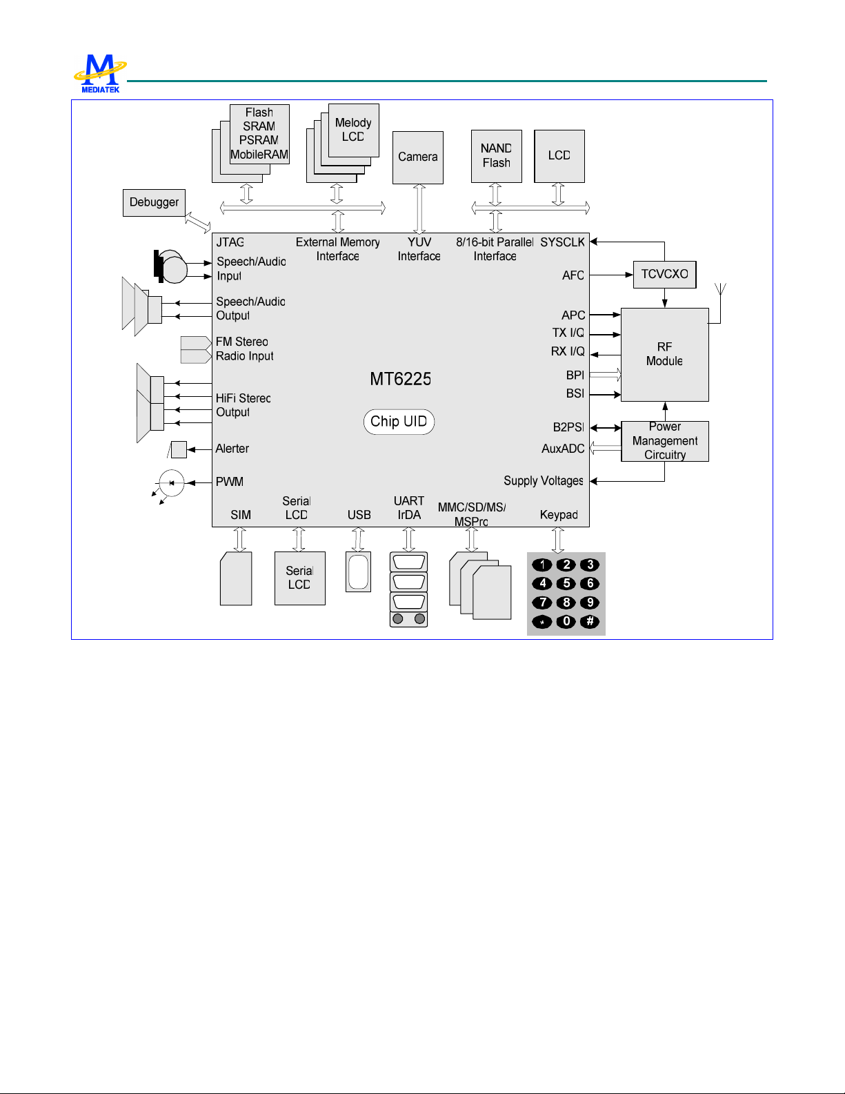
1. System Overview
The MT6225 is a highly integrated single chip soluti
GSM/GPRS phone. Based on 32-bit ARM7EJ-STM RISC
processor, MT6225 features not only high performance
GPRS Class 12 MODEM but is also designed with support
for the wireless multi-media applications, such as
advanced display engine, synthesis audio with 64-tone
polyphony, digital audio playback, Java acceleration,
MMS and etc. Additionally, MT6225 provides varieties of
advanced interfaces for functionality extensions, like
3-port external memory interface, 3-port 8/16-bit parallel
interface, NAND Flash, IrDA, USB and MMC/SD/MS/MS
Pro. The typical application can be shown as Figure 1.
Platform
MT6225 is capable of running the ARM7EJ-STM RISC
processor at up to 104 MHz, thus providing fast data
processing capabilities. In addition to the high clock
frequency, a separate CODE cache is also added to further
improve the overall system efficiency.
For large amounts of data transfer, high performance DMA
(Direct Memory Access) with hardware flow control is
implemented, which greatly enhances the data movement
speed while reducing MCU processing load.
External Memory Interface
To provide the greatest capacity for expansion and
maximum bandwidth for data intensive applications such
as multimedia features, MT6225 supports up to 3 external
state-of-the-art devices through its 8/16-bit host interface.
High performance devices such as Mobile RAM and
Cellular RAM are supported for maximum bandwidth.
Traditional devices such as burst/page mode flash, page
mode SRAM, and Pseudo SRAM are also supported. For
greatest compatibility, the memory interface can also be
used to connect to legacy devices such as Color/Parallel
LCD, and multi-media companion chips are all supported
through this interface. To minimize power consumption
and ensure low noise, this interface is designed for flexible
I/O voltage and allows lowering of the supply voltage
down to 1.8V. The driving strength is configurable for
signal integrity adjustment. The data bus also employs
on for
retention technology to prevent the bus from floating
during a turn over.
Multi-media Subsystem
In order to provide more flexibility and bandwidth for
multi-media products, an additional 8/16 bit parallel
interface is incorporated. This interface is designed
specially for support with Camera companion chip as well
as LCD panel. In addition, MT6225 has camera YUV
interface that can connect to CMOS sensor of resolution up
to VGA. Moreover, it can connect NAND flash device to
provide a solution for multi-media data storage. For
running multi-media application faster, MT6225 integrates
also several hardware-based engines. With hardware based
Resizer and advanced display engine, it can display and
combine arbitrary size of images with up to 4 blending
layers.
User Interface
For user interactions, the MT6225 brings together all
necessary peripheral blocks for multi-media GSM/GPRS
phone. It comprises the Keypad Scanner with capability of
multiple key pressing, SIM Controller, Alerter, Real Time
Clock, PWM, Serial LCD Controller and General Purpose
Programmable I/Os. For connectivity and data storage, the
MT6225 consists of UART, IrDA, USB 1.1 Slave, SDIO
and MMC/SD/MS/MS Pro.
Audio Interface
Using a highly integrated mixed-signal Audio Front-End,
the MT6225 architecture allows for easy audio interfacing
with direct connection to the audio transducers. The audio
interface integrates D/A and A/D Converters for Voice
band, as well as high resolution Stereo D/A Converters for
Audio band. In addition, MT6225 also provides Stereo
Input and Analog Mux.
MT6225 supports AMR codec to adaptively optimize
speech and audio quality. Moreover, HE-AAC codec is
implemented to deliver CD-quality audio at low bit rates.
Overall, MT6225’s audio features provide a rich platform
for multi-media applications.
6/377 MediaTek Inc. Confidential
Page 7

MT6225 GSM/GPRS Baseband Processor Data Sheet Revision 1.00
Radio Interface
MT6225 integrates a mixed-signal Baseband front-end in
order to provide a well-organized radio interface with
flexibility for efficient customization. It contains gain and
offset calibration mechanisms, and filters with
programmable coefficients for comprehensive
compatibility control on RF modules. This approach also
allows the usage of a high resolution D/A Converter for
controlling VCXO or crystal, thus reducing the need for
expensive TCVCXO. MT6225 achieves great MODEM
performance by utilizing 14-bit high resolution A/D
Converter in the RF downlink path. Furthermore, to reduce
the need for extra external current-driving component, the
driving strength of some BPI outputs is designed to be
configurable.
Debug Function
The JTAG interface enables in-circuit debugging of
software program with the ARM7EJ-S core. With this
standardized debugger interface, the MT6225 provides
developers with a wide set of options for choosing ARM
development kits from supports of thirty parties. For
security reason, JTAG interface can be disabled by
programming internal OTP (one-time programmable) fuse.
Power Management
The MT6225 offers various low-power features to help
reduce system power consumption. These features include
Pause Mode of 32KHz clocking at Standby State, Power
Down Mode for individual peripherals, and Processor
Sleep Mode. In addition, MT6225 is also fabricated in
advanced low leakage CMOS process, hence providing an
overall ultra low leakage solution.
Package
The MT6225 device is offered in a 12mm×12mm, 264-ball,
0.65 mm pitch, TFBGA package.
7/377 MediaTek Inc. Confidential
Page 8
MT6225 GSM/GPRS Baseband Processor Data Sheet Revision 1.00
Figure 1 Typical application of MT6225
8/377 MediaTek Inc. Confidential
Page 9

MT6225 GSM/GPRS Baseband Processor Data Sheet Revision 1.00
1.1 Platform Feature
General
Integrated voice-band, audio-band and base-band
TFBGA 12mm×12mm, 264-ball, 0.65 mm pitch
MCU Subsystem
ARM7EJ-S 32-bit RISC processor
High performance multi-layer AMBA bus
Java hardware acceleration for fast Java-based
ARM7EJ-S Operating frequency: 26/52/104 MHz
Dedicated DMA bus
14 DMA channels
48K Bytes on-chip SRAM
72K Bytes MCU dedicated Tightly Coupled
16K Bytes Code cache
On-chip boot ROM for Factory Flash
Watchdog timer for system crash recovery
2 sets of General Purpose Timer
Circuit Switch Data coprocessor
Division coprocessor
analog front ends
package
g
ames and applets
M
emory
Programming
Industry standard Parallel LCD Interface
Supports multi-media companion chips with 8/16
its data width
b
Flexible I/O voltage of 1.8V ~ 2.8V for memory
interface
Configurable driving strength for memory
interface
User Interfaces
6-row × 7-column keypad controller with
hardware scanner
Supports multiple key presses for gaming
SIM/USIM Controller with hardware T=0/T=1
protocol control
Real Time Clock (RTC) operating with a separate
p
ower supply
General Purpose I/Os (GPIOs)
2 Sets of Pulse Width Modulation (PWM) Output
Alerter Output with Enhanced PWM or PDM
4~10 external interrupt lines
Connectivity
3 UARTs with hardware flow control and speed up
t
o 921600 bps
IrDA modulator/demodulator with hardware
framer supports SIR mode of operation
External Memory Interface
Supports up to 3 external devices
Supports 8-bit or 16-bit memory components with
maximum size of up to 64M Bytes each
Supports Mobile RAM and Cellular RAM
Supports Flash and SRAM with Page Mode or
B
urst Mode
Supports Pseudo SRAM
9/377 MediaTek Inc. Confidential
Full-speed USB 1.1 Device controller
Multi Media Card/Secure Digital Memory
Card/Memory Stick/Memory Stick Pro host
controller
Supports SDIO interface for SDIO peripherals as
w
ell as WIFI connectivity
DAI/PCM and I2S interface for Audio application
Security
Page 10

MT6225 GSM/GPRS Baseband Processor Data Sheet Revision 1.00
Supports security key for code protection
143-bit unique/secret chip ID
Power Management
Power Down Mode for analog and digital circuits
Processor Sleep Mode
Pause Mode of 32KHz clocking at Standby State
7-channel Auxiliary 10-bit A/D Converter for
charger and battery monitoring and photo sensing
Test and Debug
Built-in digital and analog loop back modes for
both Audio and Baseband Front-End
DAI port complying with GSM Rec.11.10
JTAG port for debugging embedded MCU
10/377 MediaTek Inc. Confidential
Page 11

MT6225 GSM/GPRS Baseband Processor Data Sheet Revision 1.00
1.2 MODEM Features
Radio Interface and Baseband Front End
GMSK modulator with analog I and Q channel
outputs
10-bit D/A Converter for uplink baseband I and Q
signals
14-bit high resolution A/D Converter for downlink
baseband I and Q signals
Calibration mechanism of offset and gain
m
ismatch for baseband A/D Converter and D/A
Converter
10-bit D/A Converter for Automatic Power
Control
13-bit high resolution D/A Converter for
Automatic Frequency Control
Programmable Radio RX filter
2 Channels bi-directional Baseband Serial
I
nterface (BSI) with 3-wire or 4-wire control
GSM channel coding, equalization and A5/1, A5/2
nd A5/3 ciphering
a
GPRS GEA1, GEA2 and GEA3 ciphering
Programmable GSM/GPRS Modem
Packet Switched Data with CS1/CS2/CS3/CS4
coding schemes
GSM Circuit Switch Data
GPRS Class 12
Voice Interface and Voice Front End
Two microphone inputs sharing one low noise
amplifier with programmable gain and automatic
gain control (AGC) mechanism
Voice power amplifier with programmable gain
2nd
D/A Converter for voice downlink path
order Sigma-Delta A/D Converter for voice
uplink path
10-Pin Baseband Parallel Interface (BPI) with
programmable driving strength
Multi-band support
Voice and Modem CODEC
Dial tone generation
Voice Memo
Noise Reduction
Echo Suppression / Echo Cancellation
Advanced Sidetone Oscillation Reduction
Digital sidetone generator with programmable
g
ain
Two programmable acoustic compensation filters
GSM/GPRS quad vocoders for adaptive multirate
(
AMR), enhanced full rate (EFR), full rate (FR)
and half rate (HR)
FR error concealment
Supports half-duplex hands-free operation
Compliant with GSM 03.50
11/377 MediaTek Inc. Confidential
Page 12

MT6225 GSM/GPRS Baseband Processor Data Sheet Revision 1.00
1.3 Multi-Media Features
LCD/NAND Flash Interface
18-bit Parallel Interface supports 8/16 bit NAND
flash and 8/9/16/18 bit Parallel LCD
8/16 bit NAND Flash Controller with 1-bit ECC
correction for mass storages
2 Chip selects available for high-density NAND
flash device
Serial LCD Interface with 8/9 bit format support
LCD Controller
Hardware accelerated display
Supports simultaneous connection to up to 2
parallel LCD and 1 serial LCD modules
Supports format: RGB332, RGB444, RGB565,
RGB666, RGB888
Supports LCD panel maximum resolution up to
8
00x600 at 16bpp
HE-AAC decode support
Audio Interface and Audio Front End
Supports I2S interface
High resolution D/A Converters for Stereo Audio
playback
Stereo analog input for stereo audio source
Analog multiplexer for Stereo Audio
Stereo to Mono Conversion
FM radio recording
Supports hardware display rotation
Capable of combining display memories with up to
4 blending layers
Accelerated Gamma correction with
programmable gamma table.
Image Signal Processor
8 bit YUV format image input
Capable of processing image of size up to VGA
Flexible I/O voltage of 1.8V ~ 2.8V
Audio CODEC
Wavetable synthesis with up to 64 tones
Advanced stereo wavetable synthesizer
Wavetable including GM full set of 128
i
nstruments and 47 sets of percussions
PCM Playback and Record
Digital Audio Playback
12/377 MediaTek Inc. Confidential
Page 13

MT6225 GSM/GPRS Baseband Processor Data Sheet Revision 1.00
1.4 General Description
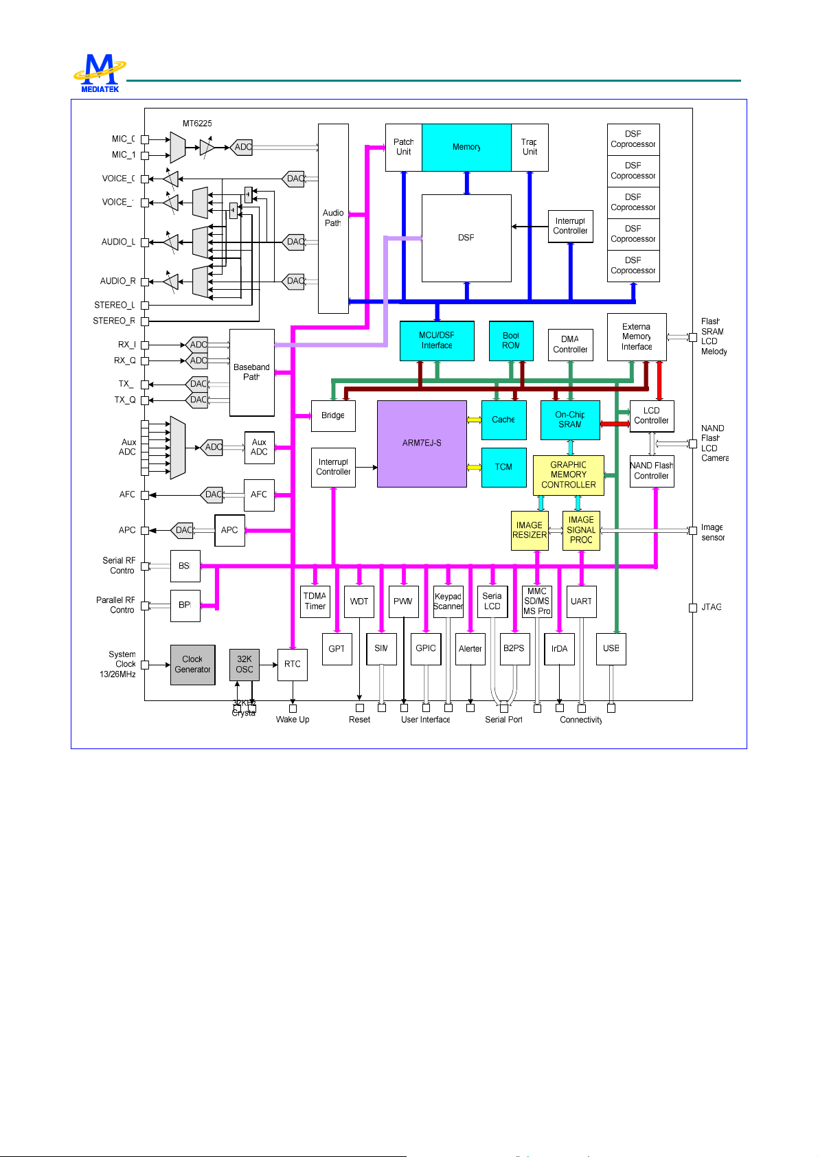
Figure 2
details the block diagram of MT6225. Based on dual-processor architecture, the major processor of MT6225
is ARM7EJ-S, which mainly runs high-level GSM/GPRS protocol software as well as multi-media applications. With
the other one is a digital signal processor corresponding for handling the low-level MODEM as well as advanced audio
functions. Except for some mixed-signal circuitries, the other building blocks in MT6225 are connected to either the
microcontroller or the digital signal processor. Specifically, MT6225 consists of the following subsystems:
Microcontroller Unit (MCU) Subsystem, including an ARM7EJ-S RISC processor and its accompanying
memory management and interrupt handling logics.
Digital Signal Processor (DSP) Subsystem, including a DSP and its accompanying memory, memory
controller, and interrupt controller.
MCU/DSP Interface, where the MCU and the DSP exchang
Microcontroller Peripherals, which include all user interface modules and RF control interface modules.
Microcontroller Coprocessors, which intend to run computing-intensive processes in place of Microcontroller.
DSP Peripherals, which are hardware accelerators for GSM/GPRS channel codec.
Multi-media Subsystem, which integrate several advanced accelerators to support multi-media applications.
Voice Front End, the data path of conveying analog s
Audio Front End, also the data path of conveying stereo audio from stereo audio source
Baseband Front End, the data path of conveying digital signal from and to analog signal of RF modules.
e hardware and software information.
peech from and to digital speech.
Timing Generator, generating the control signals related to the TDMA frame timing.
Power, Reset and Clock subsystem, managing the power, reset and clock distribution inside MT6225.
Details of the individual subsystems and blocks are described in following Chapters.
13
Page 14
MT6225 GSM/GPRS Baseband Processor Data Sheet Revision 1.00
Figure 2 MT6225 block diagram.
14
Page 15

MT6225 GSM/GPRS Baseband Processor Data Sheet Revision 1.00
2 Product Description
2.1 Pin Outs
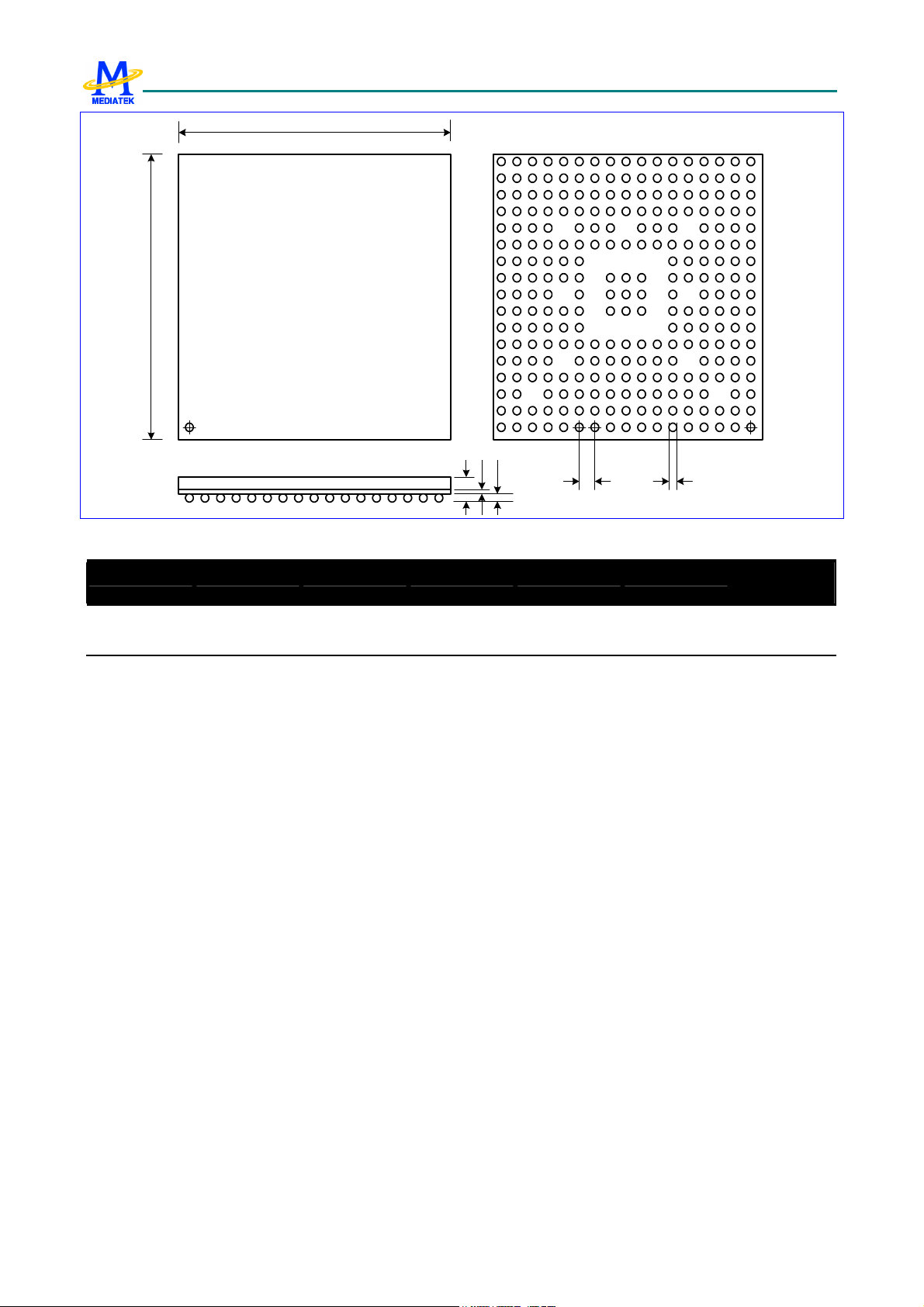
One type of package for this product, TFBGA 12mm*12mm, 264-ball, 0.65 mm pitch Package, is offered.
Pin outs and the top view are illustrated in Figure 3 for this package. Outline and dimension of package is illustrated in
Figure 4, while the definition of package is shown in Table 1.
15
Page 16

MT6225 GSM/GPRS Baseband Processor Data Sheet Revision 1.00
14131211106321 87 954
AVSS_
XOUT
A
XIN
B
RIN
C
AVSS_
D
RTC
JTMS
E
JRTCK
F
BSI_D
G
ATA
BSI_C
H
LK
LSCE0
J
#
K
L
M
SYSCL
PLL
AVDD_
BBWA
RTC
KEUP
JTRST
TESTM
#
JTCK
BPI_B
JTDO
BPI_B
BPI_B
US2
BPI_B
BSI_C
S0
LPCE1
LSCE1
#
LRD#LRST# LPA0
NLD14NLD13NLD12
NLD8
K
ODE
JTDI
US0
US3
US9
#
AFC
AVSS_
RFE
AFC_B
YP
PLL_O
UT
BPI_B
US1
BPI_B
US4
BPI_B
US8
LPCE0
#
LWR#
NLD15
NLD10
APC
AUXA
DIN1
AUXA
DIN3
AUXA
DIN5
BPI_B
US5
BPI_B
US7
VDD33LSDALSCK LSA0
NLD17
NLD16
NLD11NLD9NLD7
AGND
_RFE
AUXA
DIN0
AUXA
DIN2
AUXA
DIN4
AUXA
DIN6
BPI_B
US6
VDDK
VDD33
VDDK
VSS33
VDD33
VDD33
_EMI
BDLA
AU_VI
QP
N1_N
BDLA
AU_VI
QN
N0_P
AGND
BDLAI
_AFE
N
AU_VR
BDLAI
EF_PI
P
AVDD_
AVCC_
GSMR
PLL
FTX
AUX_R
AVDD_
EF
RFE
VSS33
VPP
WATC
HDOG
MT6225 TFBGA
VDD33
VSS33
_EMI
AVDD_
AFE
AU_VI
N0_P
AU_VI
N0_P
AU_VR
EF_NI
AVSS_
AFE
AVSS_
GSMR
FTX
VSS33
_USB
USB_D
P
T
op-View
VSS33
_EMI
AU_O
UT0_N
AU_O
UT0_P
AU_MI
CBIAS
_P
AU_MI
CBIAS
_N
AVDD_
BUF
AVSS_
BUF
VSS33
VSS33
USB_D
M
VSS33
_EMI
AU_M
OUTR
AVSS_
MBUF
AU_F
MINL
AU_F
MINR
AVDD_
MBUF
VDDK
AU_M
OUTL
CMDA
T0
CMDA
T1
CMDA
T2
VDD33
_CAM
VDDKVSSK
VDDK
VDD33
VDD33
VDD33
_USB
VSS33
_EMI
VDD33
_EMI
CMDA
T3
CMDA
T4
CMDA
T5
GPIO6
GPIO5
GPIO4
VDD33
VDD33
_MC
VSS33
_EMI
MCCM
0
CMDA
T6
CMDA
T7
CMHR
EF
GPIO7
KROW
1
KROW
5
KCOL3
UTXD2
SIMDA
TA
SIMRS
T
MCDA
0
ED0
CMVR
EF
CMPD
N
CMRS
T
DAIPC
MOUT
KROW
2
SIMSE
L
MCINS
MCDA
1
ED1
GPIO9
GPIO8
DAISY
NC
DAICL
K
KROW
3
SIMVC
C
MCDA
2
171615
CMPC
LK
CMMC
LK
DAIPC
MIN
KROW
0
KROW
4
KCOL2KCOL1KCOL0
URXD3UTXD3KCOL4
URXD1UTXD1URXD2
SIMCL
K
MCCKMCWP
MCDA
3
ED3ED2
A
B
C
D
E
F
G
H
J
K
L
M
NLD3
N
NRNB
P
NEW# EINT1
R
NREB
T
NCE#
U
SRCL
KENAI
SRCL
KENA
NLD5NLD4
NLD1NLD0 EINT2NLD2
GPIO0
SYSRS
T#
NLD6
NCLENALE
GPIO2
GPIO1
VSS33
VDDK
_EMI
EA23
EA19
EA20 EA16
EA24 ED12EA4
EINT0 EA25
GPIO3 EINT3
EA21 EA17
VDD33
_EMI
EA18
VSS33
_EMI
EA12
EA13
VSS33
_EMI
EA8
EA9
EA2
EA5
EA6
EPDN_
B
ECLKEA3EA7EA11EA15
EWAIT
EA1
ED4
EWR#
EUB#
ERD#ECS0#EADV#
EDCL
ECS2# ECS1#
K
ECKE ED14
ERAS# ECAS#
Figure 3 Top View of MT6225 TFBGA 12mm*12mm, 264-ball, 0.65 mm pitch Package
ED5
14131211106321 87 954 171615
ED6
ED9ED8
ED11
ED15
ELB#EA22 EA10EA14
ED7
ED10
ED13
N
P
R
T
U
16
Page 17
MT6225 GSM/GPRS Baseband Processor Data Sheet Revision 1.00
D
E
MT6225
Top View
(Pins Down)
A C A1
151617
MT6225
Bottem View
e b
Figure 4 Outlines and Dimension of TFBGA 12mm*12mm, 264-ball, 0.65 mm pitch Package
15 4 3 2610 9 8 711121314
A
B
C
D
E
F
G
H
J
K
L
M
N
P
R
T
U
Body Size Ball Count Ball Pitch Ball Dia. Package Thk. Stand Off Substrate
Thk.
D E N e b A (Max.) A1 C
12 12 264 0.65 0.3 1.2 0.21 0.36
Table 1 Definition of TFBGA 12mm*12mm, 264-ball, 0.65 mm pitch Package (Unit: mm)
17
Page 18

MT6225 GSM/GPRS Baseband Processor Data Sheet Revision 1.00
2.2 Top Marking Definition
MT 62 25
DD DD -# # #
LL LL L
S
Figure 5 MT6225A top marking
MT6225: Part No.
DDDD: Date Code
###: Subcontractor Code
LLLLL: Lot No.
S: Special Code
18
Page 19

MT6225 GSM/GPRS Baseband Processor Data Sheet Revision 1.00
2.3 DC Characteristics
2.3.1 Absolute Maximum Ratings
Prolonged exposure to absolute maximum ratings may reduce device reliability. Functional operation at these
maximum ratings is not implied.
Item Symbol Min Max Unit
IO power supply VDD33 -0.3 VDD33+0.3 V
I/O input voltage VDD33I -0.3 VDD33+0.3 V
Operating temperature Topr -20 80 Celsius
Storage temperature Tstg -55 125 Celsius
19
Page 20
MT6225 GSM/GPRS Baseband Processor Data Sheet Revision 1.00
2.4 Pin Description
Ball
12X12
C2
D2
D3
E1
E2
F1
E3
E4
F2
F3
F4
F5
F6 BPI_BUS6 IO RF hard-wire control bus 6
G5 BPI_BUS7 IO RF hard-wire control bus 7
G4 BPI_BUS8 IO RF hard-wire control bus 8
G3 BPI_BUS9 IO RF hard-wire control bus 9
G2
G1
H1
H2 LSCK IO Serial display interface data
H3 LSA0 IO Serial display interface address
H4 LSDA IO Serial display interface clock
J1 LSCE0# IO Serial display interface chip
J2 LSCE1# IO Serial display interface chip
J3 LPCE1# IO Parallel display interface chip
J4
K1
Name Dir Description
JTRST#
JTCK
JTDI
JTMS
JTDO
JRTCK
BPI_BUS0
BPI_BUS1
BPI_BUS2
BPI_BUS3
BPI_BUS4
BPI_BUS5
BSI_CS0
BSI_DATA
BSI_CLK
LPCE0#
LRST#
JTAG Port
I JTAG test port reset input PD Inpu
I JTAG test port clock input PU Inpu
I JTAG test port data input PU Inpu
I JTAG test port mode switch PU Inpu
O JTAG test port data output PU 0
O JTAG test port returned clock
output
RF Parallel Control Unit
O RF hard-wire control bus 0 0
O RF hard-wire control bus 1 0
O RF hard-wire control bus 2 0
O RF hard-wire control bus 3 0
O RF hard-wire control bus 4
O RF hard-wire control bus 5
RF Serial Control Unit
O RF 3-wire interface chip select 0 0
O RF 3-wire interface data output 0
O RF 3-wire interface clock output 0
Serial LCD/PM IC Interface
output
output
output
select 0 output
select 1 output
Parallel LCD/Nand-Flash
Interface
select 1 output
O Parallel display interface chip
select 0 output
O Parallel display interface Reset
Signal
PU
Reset IO
Mode0 Mode1 Mode2 Mode3
PU 0
GPIO25
GPIO26
GPIO27
GPIO28
GPIO29
GPIO30
GPIO31
GPIO32
GPIO33
GPIO34
0
0
BPI_BUS6 PWM1 13MHz PD Inpu
BPI_BUS7 PWM2 32KHz PD Inpu
BPI_BUS8 ALERTER 26MHz PD Inpu
BPI_BUS9 BSI_CS1 PD Inpu
LSCK TDMA_CK DSP_TID0 PU Inpu
LSA0 TDMA_D1 TDTIRQ PU Inpu
LSDA TDMA_D0 TCTIRQ2 PU Inpu
LSCE0# TDMA_FS TCTIRQ1 PU Inpu
LSCE1# LPCE2# TEVTVAL PU Inpu
LPCE1# NCE1# PU Inpu
1
1
/P
D
t
t
t
t
t
t
t
t
t
t
t
t
t
t
power
VDD33
VDD33
VDD33
VDD33
VDD33
20
Page 21

MT6225 GSM/GPRS Baseband Processor Data Sheet Revision 1.00
K2
K3
K4
K5 NLD17 IO Parallel LCD/Nand-Flash Data 17
L5 NLD16 IO Parallel LCD/Nand-Flash Data 16
L4
L3
L2
L1
M5
M4
M3
M2
M1
N4
N3
N2
N1
P4
P3
P2
P1 NRNB IO Nand-Flash Read/Busy Flag
R4 NCLE IO Nand-Flash Command Latch
R2 NALE IO Nand-Flash Address Latch Signal
R1 NWE# IO Nand-Flash Write Strobe
T1 NRE# IO Nand-Flash Read Strobe
U1 NCE# IO Nand-Flash Chip select output
K14
J17
J16
J15 SIMSEL IO SIM card supply power select
LRD#
LPA0
LWR#
NLD15
NLD14
NLD13
NLD12
NLD11
NLD10
NLD9
NLD8
NLD7
NLD6
NLD5
NLD4
NLD3
NLD2
NLD1
NLD0
SIMRST
SIMCLK
SIMVCC
O Parallel display interface Read
Strobe
O Parallel display interface address
output
O Parallel display interface Write
Strobe
IO Parallel LCD/Nand-Flash Data 15
IO Parallel LCD/Nand-Flash Data 14
IO Parallel LCD/Nand-Flash Data 13
IO Parallel LCD/Nand-Flash Data 12
IO Parallel LCD/Nand-Flash Data 11
IO Parallel LCD/Nand-Flash Data 10
IO Parallel LCD/Nand-Flash Data 9
IO Parallel LCD/Nand-Flash Data 8
IO Parallel LCD/Nand-Flash Data 7
IO Parallel LCD/Nand-Flash Data 6
IO Parallel LCD/Nand-Flash Data 5
IO Parallel LCD/Nand-Flash Data 4
IO Parallel LCD/Nand-Flash Data 3
IO Parallel LCD/Nand-Flash Data 2
IO Parallel LCD/Nand-Flash Data 1
IO Parallel LCD/Nand-Flash Data 0
Signal
SIM Card Interface
O SIM card reset output 0
O SIM card clock output 0
O SIM card supply power control 0
GPIO35
GPIO36
GPIO37
GPIO38
GPIO39
GPIO40
GPIO41
GPIO42
GPIO46
1
1
1
NLD17 KCOL5 VPP65 PD Inpu
t
NLD16 KCOL6 PD Inpu
t
PD Inpu
t
PD Inpu
t
PD Inpu
t
PD Inpu
t
PD Inpu
t
PD Inpu
t
PD Inpu
t
PD Inpu
t
PD Inpu
t
PD Inpu
t
PD Inpu
t
PD Inpu
t
PD Inpu
t
PD Inpu
t
PD Inpu
t
PD Inpu
t
NRNB DSP_TID1 PU Inpu
t
NCLE DSP_TID2 PD Inpu
t
NALE DSP_TID3 PD Inpu
t
NWE# DSP_TID4 PU Inpu
t
NRE# DSP_TID5 PU Inpu
t
NCE# DSP_TID6 PU Inpu
t
SIMSEL PD Inpu
VDD33
21
Page 22

MT6225 GSM/GPRS Baseband Processor Data Sheet Revision 1.00
J14
T3
U4
T4
U5
G13
F13
D13
D14
B16
A16
U3
K8
U2
T2 SRCLKENAI IO External TCXO enable input
G15
G14
F17
F16
F15
F14
E17
E16
E15
E14
D17
T5
R5
P5
U6
SIMDATA
GPIO0
GPIO1
GPIO2
GPIO3
GPIO4
GPIO5
GPIO6
GPIO7
GPIO8
GPIO9
SYSRST#
WATCHDOG
SRCLKENA
KCOL4
KCOL3
KCOL2
KCOL1
KCOL0
KROW5
KROW4
KROW3
KROW2
KROW1
KROW0
EINT0
EINT1
EINT2
EINT3
IO SIM card data input/output 0
Dedicated GPIO Interface
IO General purpose input/output 0
IO General purpose input/output 1
IO General purpose input/output 2
IO General purpose input/output 3
IO General purpose input/output 4
IO General purpose input/output 5
IO General purpose input/output 6
IO General purpose input/output 7
IO General purpose input/output 8
IO General purpose input/output 9
Miscellaneous
I System reset input active low Inpu
O Watchdog reset output 1
O External TCXO enable output
active high
Keypad Interface
I Keypad column 4 PU Inpu
I Keypad column 3 PU Inpu
I Keypad column 2 PU Inpu
I Keypad column 1 PU Inpu
I Keypad column 0 PU Inpu
O Keypad row 5 0
O Keypad row 4 0
O Keypad row 3 0
O Keypad row 2 0
O Keypad row 1 0
O Keypad row 0 0
External Interrupt Interface
I External interrupt 0 PU Inpu
I External interrupt 1 PU Inpu
I External interrupt 2 PU Inpu
I External interrupt 3 PU Inpu
External Memory Interface
t
GPIO0
GPIO1
GPIO2
GPIO3
GPIO4
GPIO5
GPIO6
GPIO7
GPIO8
GPIO9
GPO0
GPIO43
22
EINT4 PU Inpu
t
EINT5 PU Inpu
t
UCTS1 EINT6 PU Inpu
t
BSI_RFIN URTS1 EINT7 PU Inpu
t
DAIRST IRDA_PDN DSP_CLK PU Inpu
t
EDICK 26MHz AHB_CLK PD Inpu
t
EDIWS 32KHz ARM_CLK PD Inpu
t
EDIDAT SLOW_C
LK
SCL PU Inpu
SDA PU Inpu
SRCLKE
NA
SRCLKE
NAI
1
PD Inpu
PD Inpu
t
t
t
t
t
t
t
t
t
t
t
t
t
t
VDD33
VDD33
_CAM
VDD33
VDD33
VDD33
Page 23

MT6225 GSM/GPRS Baseband Processor Data Sheet Revision 1.00
M14
M15
M16
M17
N14
N15
N16
N17
P15
P16
P17
R16
R17
T17
U17
T16
R14
P13
R13
T15
T14
U16
P14
N12
R12
T12
P12
U14
U15
U13
T13
U12
N11
P11
R11
ED0
ED1
ED2
ED3
ED4
ED5
ED6
ED7
ED8
ED9
ED10
ED11
ED12
ED13
ED14
ED15
ERD#
EWR#
ECS0#
ECS1#
ECS2#
ELB#
EUB#
EPDN#
EADV#
EWAIT
ECLK
ERAS#
ECAS#
ECKE
EDCLK
EA1
EA2
EA3
EA4
IO External memory data bus 0 Inpu
t
IO External memory data bus 1 Inpu
t
IO External memory data bus 2 Inpu
t
IO External memory data bus 3 Inpu
t
IO External memory data bus 4 Inpu
t
IO External memory data bus 5 Inpu
t
IO External memory data bus 6 Inpu
t
IO External memory data bus 7 Inpu
t
IO External memory data bus 8 Inpu
t
IO External memory data bus 9 Inpu
t
IO External memory data bus 10 Inpu
t
IO External memory data bus 11 Inpu
t
IO External memory data bus 12 Inpu
t
IO External memory data bus 13 Inpu
t
IO External memory data bus 14 Inpu
t
IO External memory data bus 15 Inpu
t
O External memory read strobe 1
O External memory write strobe 1
O External memory chip select 0 1
O External memory chip select 1 1
O External memory chip select 2 1
O External memory lower byte
strobe
O External memory upper byte
strobe
O Power Down Control Signal for
PSRAM
O Address valid for burst mode
flash memory
I External device wait signal Inpu
O Clock for flash memory 0
O Mobile SDRAM row address
strobe
O Mobile SDRAM column address
strobe
O Mobile SDRAM clock enable 0
O Mobile SDRAM clock 0
O External memory address bus 1 0
O External memory address bus 2 0
O External memory address bus 3 0
O External memory address bus 4 0
GPO3
1
1
1
EPDN#
1
1
6.5MHz 26MHz 0*
t
VDD33
_EMI
23
Page 24

MT6225 GSM/GPRS Baseband Processor Data Sheet Revision 1.00
T11
U11
P10
R10
T10
U10
P9
R9
T9
U9
P8
R8
T8
U8
P7
R7
T7
U7
P6
R6
T6
K9
K10
M13
L14
L15
L16
L17
K17
K16 MCWP IO SD Write Protect Input
K15 MCINS IO SD Card Detect Input
H17
H16
H15 URXD2 IO UART 2 receive data
H14 UTXD2 IO UART 2 transmit data
G17 URXD3 IO UART 3 receive data
G16 UTXD3 IO UART 3 transmit data
D16 DAICLK IO DAI clock output
D15 DAIPCMOUT IO DAI pcm data out
C17 DAIPCMIN IO DAI pcm data input
EA5
EA6
EA7
EA8
EA9
EA10
EA11
EA12
EA13
EA14
EA15
EA16
EA17
EA18
EA19
EA20
EA21
EA22
EA23
EA24
EA25
USB_DP
USB_DM
MCCM0
MCDA0
MCDA1
MCDA2
MCDA3
MCCK
URXD1
UTXD1
O External memory address bus 5 0
O External memory address bus 6 0
O External memory address bus 7 0
O External memory address bus 8 0
O External memory address bus 9 0
O External memory address bus 10 0
O External memory address bus 11 0
O External memory address bus 12 0
O External memory address bus 13 0
O External memory address bus 14 0
O External memory address bus 15 0
O External memory address bus 16 0
O External memory address bus 17 0
O External memory address bus 18 0
O External memory address bus 19 0
O External memory address bus 20
O External memory address bus 21
O External memory address bus 22 0
O External memory address bus 23 0
O External memory address bus 24 GPO1
O External memory address bus 25 GPO2
USB Interface
IO USB D+ Input/Output
IO USB D- Input/Output
Memory Card Interface
IO SD Command/MS Bus State
Output
IO SD Serial Data IO 0/MS Serial
Data IO
IO SD Serial Data IO 1
IO SD Serial Data IO 2
IO SD Serial Data IO 3
O SD Serial Clock/MS Serial Clock
Output
UART Interface
I UART 1 receive data
O UART 1 transmit data
Digital Audio Interface
EA24
EA25
GPIO44
GPIO45
GPIO35
GPIO36
GPIO33
GPIO34
GPIO51
GPIO52
GPIO53
MCWP PU
MCINS PU
URXD2 UCTS3 IRDA_R
UTXD2 URTS3 IRDA_T
URXD3 UCTS2 PU Inpu
UTXD3 URTS2 PU Inpu
DAICLK PU Inpu
DAIPCM
OUT
DAIPCMIN PU Inpu
26MHz 32KHz 0
32KHz 26MHz 0
XD
XD
PD Inpu
0
0
PU Inpu
t
1
PU Inpu
t
PU Inpu
t
t
t
t
t
t
VDD33
_USB
VDD33
_MC
VDD33
VDD33
24
Page 25

MT6225 GSM/GPRS Baseband Processor Data Sheet Revision 1.00
sensor power down control
C16 DAISYNC IO DAI frame synchronization signal
output
C15 CMRST IO Image sensor reset signal output
B15 CMPDN IO Image
A15 CMVREF IO Sensor vertical reference signal
C14 CMHREF IO Sensor horizontal reference signal
A17
B17 CMMCLK IO Image sensor master clock output
B14 CMDAT7 IO Image sensor data input 7
A14 CMDAT6 IO Image sensor data input 6
C13 CMDAT5 IO Image sensor data input 5
B13 CMDAT4 IO Image sensor data input 4
A13 CMDAT3 IO Image sensor data input 3
D12 CMDAT2 IO Image sensor data input 2
C12 CMDAT1 IO Image sensor data input 1
B12 CMDAT0 IO Image sensor data input 0
A12
A11
C11
D11
A10
B19
C10
D10
D9
D8
B9
C9
A8
B8
A7
B7
C7
D7
CMPCLK
AU_MOUL
AU_MOUR
AU_FMINL
AU_FMINR
AU_OUT0_N
AU_OUT0_P
AU_MICBIAS
_P
AU_MICBIAS
_N
AU_VREF_N
AU_VREF_P
AU_VIN0_P
AU_VIN0_N
AU_VIN1_N
AU_VIN1_P
BDLAQP/BU
PAQP
BDLAQN/BU
PAQN
BDLAIN/BUP
AIN
BDLAIP/BUP
Image Sensor Interface
input
input
I Image sensor pixel clock input
Analog Interface
Audio analog output left channel
Audio analog output right
channel
FM radio analog input left
channel
FM radio analog input right
channel
Earphone 0 amplifier output (-)
Earphone 0 amplifier output (+)
Microphone bias supply (+)
Microphone bias supply (-)
Audio reference voltage (-)
Audio reference voltage (+)
Microphone 0 amplifier input (+)
Microphone 0 amplifier input (-)
Microphone 1 amplifier input (-)
Microphone 1 amplifier input (+)
Quadrature input (Q+) baseband
codec downlink/uplink
Quadrature input (Q-) baseband
codec downlink/uplink
In-phase input (I+) baseband
codec downlink/uplink
In-phase input (I-) baseband
GPIO54
GPIO10
GPIO11
GPIO12
GPIO13
GPIO14
GPIO15
GPIO16
GPIO17
GPIO18
GPIO19
GPIO20
GPIO21
GPIO22
DAISYNC PU Inpu
t
CMRST PD Inpu
t
CMPDN PD Inpu
t
MIRQ PU/
MFIQ PU/
Inpu
CMMCLK 26MHz 6.5MHz Outp
CMDAT7 MCDA7 Inpu
CMDAT6 MCDA6 DICK Inpu
CMDAT5 MCDA5 DID Inpu
CMDAT4 MCDA4 DIMS Inpu
CMDAT3 DSP_GPO3 TBTXEN Inpu
CMDAT2 DSP_GPO2 TBTXFS Inpu
CMDAT1 DSP_GPO1 TBRXEN PD Inpu
CMDAT0 DSP_GPO0 TBRXFS PD Inpu
PD
PD
Inpu
t
Inpu
t
t
ut
t
t
t
t
t
t
t
t
VDD33
_CAM
25
Page 26

MT6225 GSM/GPRS Baseband Processor Data Sheet Revision 1.00
AIP
A5
B6
B5
C6
C5
D6
D5
E6
F7
A4
C4
A3
D4
A1
B1
C1
B3
C3
F12
G6
J6
G12
N6
M11
M6
M8
N8
M12
N7
M9
N9
M10
N10
L12
L13
APC
AUXADIN0
AUXADIN1
AUXADIN2
AUXADIN3
AUXADIN4
AUXADIN5
AUXADIN6
AUX_REF
AFC
AFC_BYP
SYSCLK
PLL_OUT
XOUT
XIN
RIN
BBWAKEUP
TESTMODE
VDDK
VDDK
VDDK
VDDK
VDDK
VDDK
VDD33_EMI
VDD33_EMI
VDD33_EMI
VDD33_EMI
VSS33_EMI
VSS33_EMI
VSS33_EMI
VSS33_EMI
VSS33_EMI
VSS33_EMI
VSS33_EMI
codec downlink/uplink
Automatic power control DAC
output
Auxiliary ADC input 0
Auxiliary ADC input 1
Auxiliary ADC input 2
Auxiliary ADC input 3
Auxiliary ADC input 4
Auxiliary ADC input 5
Auxiliary ADC input 6
Auxiliary ADC reference voltage
input
Automatic frequency control
DAC output
Automatic frequency control
DAC bypass capacitance
VCXO Interface
13MHz or 26MHz system clock
input
PLL test pin
RTC Interface
32.768 KHz crystal output
32.768 KHz crystal input
32.768 KHz crystal gain control
resistor
O Baseband power on/off control 1
I TESTMODE enable input
Supply Voltages
Supply voltage of internal logic
Supply voltage of internal logic
Supply voltage of internal logic
Supply voltage of internal logic
Supply voltage of internal logic
Supply voltage of internal logic
Supply voltage of memory
interface driver
Supply voltage of memory
interface driver
Supply voltage of memory
interface driver
Supply voltage of memory
interface driver
Ground of memory interface
driver
Ground of memory interface
driver
Ground of memory interface
driver
Ground of memory interface
driver
Ground of memory interface
driver
Ground of memory interface
driver
Ground of memory interface
driver
PD Inpu
t
AVCC_
PLL
AVDD_
RTC
Typ.
1.8V
Typ.
1.8~2.8V
26
Page 27

MT6225 GSM/GPRS Baseband Processor Data Sheet Revision 1.00
K12
K13
J9
E12
H5
H6
L6
J12
H13
H12
H8
K6
M7
J10
H10
F11
J8
B2
D1
E7
A2
E11
B11
E10
F10
A9
C8
F9
A6
H9
E8
B4
F8
VDD33_USB
VDD33_MC
VSS33_USB/
MC
VDD33_CAM
VDD33
VDD33
VDD33
VDD33
VDD33
VDD33
VSS33
VSS33
VSS33
VSS33
VSS33
VSSK
VPP
AVDD_RTC
AVSS_RTC
AVCC_PLL
AVSS_PLL
AVDD_MBUF
AVSS_MBUF
AVDD_BUF
AVSS_BUF
AVDD_AFE
AGND_AFE
AVSS_AFE
AGND_RFE
AVSS_GSMR
FTX
AVDD_GSMR
FTX
AVSS_RFE
AVDD_RFE
Supply voltage of USB
transceiver
Supply voltage of memory card
interface drivers
Ground of USB/memory card
interface
Supply voltage of image sensor
interface drivers
Supply voltage for pad
Supply voltage for pad
Supply voltage for pad
Supply voltage for pad
Supply voltage for pad
Supply voltage for pad
Ground
Ground
Ground
Ground
Ground
Ground
Supply voltage for OTP
programming
Supply voltage for Real Time
Clock
Ground for Real Time Clock
Analog Supplies
Supply voltage for PLL Typ.
Ground for PLL supply
Supply Voltage for Audio band
section
GND for Audio band section
Supply voltage for voice band
transmit section
GND for voice band transmit
section
Supply voltage for voice band
receive section
GND reference voltage for voice
band section
GND for voice band receive
section
GND reference voltage for
baseband section, APC, AFC and
AUXADC
GND for baseband transmit
section
Supply voltage for baseband
transmit section
GND for baseband receive
section, APC, AFC and
AUXADC
Supply voltage for baseband
receive section, APC, AFC and
AUXADC
Typ.
3.3V
Typ.
2.8V
Typ.
Typ.
Typ.
Typ.
Typ.
Typ.
Typ.
1.8~2.8
V
Typ.
2.8V
1.8~6.5V
1.5V
1.8V
2.8V
2.8V
2.8V
2.8V
Typ.
2.8V
Table 2 Pin Descriptions (Bolded types are functions at reset)
27
Page 28

MT6225 GSM/GPRS Baseband Processor Data Sheet Revision 1.00
*Note: The state of EPDN# during the system reset is low, and it changes to high after the system reset is released.
28
Page 29

MT6225 GSM/GPRS Baseband Processor Data Sheet Revision 1.00
2.5 Ordering information
2.5.1 MT6225A
Part number Package Operational temperature range
MT6225A/ACS 12x12x1.2 mm 264-TFBGA -20~80°C
MT6225A/ACS-L 12x12x1.2 mm 264-TFBGA (Pb free) -20~80°C
Table 3 MT6225A ordering information
29
Page 30

MT6225 GSM/GPRS Baseband Processor Data Sheet Revision 1.00
3 Micro-Controller Unit Subsystem
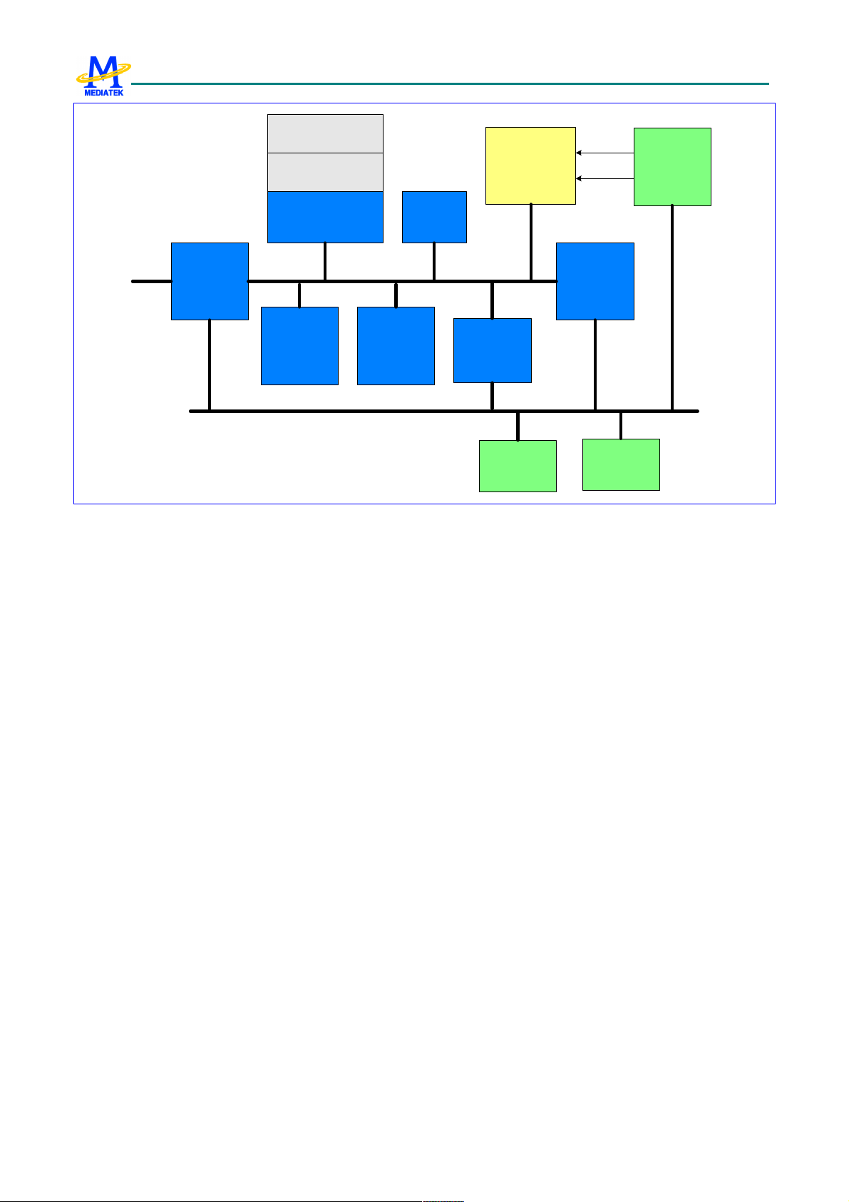
Figure 6 illustrates the block diagram of the Micro-Controller Unit Subsystem in MT6225. The subsystem utilizes a
main 32-bit ARM7EJ-S RISC processor, which plays the role of the main bus master controlling the whole subsystem.
All processor transactions go to code cache first. The code cache controller accesses TCM (72KB memory dedicated
to ARM7EJS core), cache memory, or bus according to the processor’s request address. If the requested content is
found in TCM or in cache, no bus transaction is required. If the code cache hit rate is high enough, bus traffic can be
effectively reduced and processor core performance maximized. In addition to the benefits of reuse of memory
contents, code cache also has a MPU (Memory Protection Unit), which allows cacheable and protection settings of
predefined regions. The contents of code cache are only accessible to MCU, and only MCU instructions are kept in
the cache memory (thus the name “code” cache).
The bus comprises of two-level system buses: Advanced High-Performance Bus (AHB) and Advanced Peripheral Bus
(APB). All bus transactions originate from bus masters, while slaves can only respond to requests from bus masters.
Before data transfer can be established, the bus master must ask for bus ownership, accomplished by request-grant
handshaking protocol between masters and arbiters.
Two levels of bus hierarchy are designed to provide optimum usage for different performance requirements.
Specifically, AHB Bus, the main system bus, is tailored toward high-speed requirements and provides 32-bit data path
with multiplex scheme for bus interconnections. The APB Bus, on the other hand, is designed to reduce interface
complexity for lower data transfer rate, and so it is isolated from high bandwidth AHB Bus by APB Bridge. APB Bus
supports 16-bit addressing and both 16-bit and 32-bit data paths. APB Bus is also optimized for minimal power
consumption by turning off the clock when there is no APB bus activity.
During operation, if the target slave is located on AHB Bus, the transaction is conducted directly on AHB Bus.
However, if the target slave is a peripheral and is attached to the APB bus, then the transaction is conducted between
AHB and APB bus through the use of APB Bridge.
The MT6225 MCU subsystem supports only memory addressing method. Therefore all components are mapped onto
the MCU 32-bit address space. A Memory Management Unit is employed to allow for a central decode scheme.
The MMU generates appropriate selection signals for each memory-addressed module on the AHB Bus.
In order to off-load the processor core, a DMA Controller is designated to act as a master and share the bus resources
on AHB Bus to do fast data movement between modules. This controller comprises thirteen DMA channels.
The Interrupt Controller provides a software interface to manipulate interrupt events. It can handle up to 32 interrupt
sources asserted at the same time. In general, it generates 2 levels of interrupt requests, FIQ and IRQ, to the processor.
A 128K Byte SRAM is provided for acting as system memory for high-speed data access. For factory programming
purpose, a Boot ROM module is used. These two modules use the same Internal Memory Controller to connect to AHB
Bus.
External Memory Interface supports both 8-bit and 16-bit devices. Since AHB Bus is 32-bit wide, all the data transfer
will be converted into several 8-bit or 16-bit cycles depending on the data width of target device. Note that, this
interface is specific to both synchronous and asynchronous components, like Flash, SRAM and parallel LCD. This
interface supports also page and burst mode type of Flash.
30
Page 31
MT6225 GSM/GPRS Baseband Processor Data Sheet Revision 1.00
System ROM
ARM7EJ-S
DMA
Controller
Peripheral
Ext
Bus
External
Memory
Interface
System RAM
Internal Memory
Controller
MCU-DSP
Interface
Arbiter
AHB Bus
USB
Figure 6 Block Diagram of the Micro-Controller Unit Subsystem in MT6225
Interrupt
Controller
APB
Bridge
APB Bus
Peripheral
3.1 Processor Core
3
.1.1 General Description
The Micro-Controller Unit Subsystem in MT6225 is built up with a 32-bit RISC core, ARM7EJ-S that is based on Von
Neumann architecture with a single 32-bit data bus carrying both instructions and data. The memory interface of
ARM7EJ-S is totally compliant to AMBA based bus system. Basically, it can be connected to AHB Bus directly.
3.2 Memory Management
3.2.1 General Description
The processor core of MT6225, ARM7EJ-S, supports onl
access. It manages a 32-bit address space that has addressing capability up to 4GB. System RAM, System ROM,
Registers, MCU Peripherals and external components are all mapped onto such 32-bit address space, as depicted in
Figure 7.
y memory addressing method for instruction fetch and data
31
Page 32
MT6225 GSM/GPRS Baseband Processor Data Sheet Revision 1.00
MCU 32-bit
Addressing
Space
AFFF_FFFh
|
A000_0000h
9FFF_FFFh
|
9000_0000h
8FFF_FFFFh
|
8000_0000h
7FFF_FFFFh
|
7000_0000h
6FFF_FFFFh
|
5000_0000h
9800_0000h
9000_0000h LCD
7800_0000h
7000_0000h USB
Reserved
TCM
Reserved
APB Peripherals
Virtual FIFO
MCU-DSP Interface
4FFF_FFFFh
|
4000_0000h
3FFF_FFFFh
|
0000_0000h
Internal Memory
External Memroy
EA[25:0]
Addressing
Space
Figure 7 The Memory Layout of MT6225
The address space is organized as basis of blocks with size of 256M Bytes for each. Memory blocks MB0-MB9 are
determined and currently dedicated to specific functions, as shown in Table 4, while the others are reserved for future
usage. Essentially, the block number is uniquely selected by address line A31-A28 of internal system bus.
Memory
Block
MB0 0h
Block Address
A31-A28
Address Range Description
00000000h-07FFFFFFh Boot Code, EXT SRAM or EXT Flash/MISC
08000000h-0FFFFFFFh EXT SRAM or EXT Flash/MISC
MB1 1h
10000000h-17FFFFFFh EXT SRAM or EXT Flash/MISC
18000000h-1FFFFFFFh Reserved
MB2 2h
20000000h-27FFFFFFh Reserved
28000000h-2FFFFFFFh Reserved
MB3 3h
30000000h-37FFFFFFh Reserved
38000000h-3FFFFFFFh Reserved
MB4 4h
40000000h-47FFFFFFh System RAM
48000000h-4FFFFFFFh System ROM
MB5 5h 50000000h-5FFFFFFFh MCU-DSP Interface
32
Page 33

MT6225 GSM/GPRS Baseband Processor Data Sheet Revision 1.00
MB6 6h 60000000h-6FFFFFFFh
MB7 7h
70000000h-77FFFFFFh USB
78000000h-7FFFFFFFh Virtual FIFO
MB8 8h 80000000h-8FFFFFFFh APB Slaves
MB9 9h
90000000h-97FFFFFFh LCD
98000000h-9FFFFFFFh Reserved
MB10 Ah A0000000h-AFFFFFFFh TCM
Table 4 Definitions of Memory Blocks in MT6225
3.2.1.1 External Access
To have external access, the MT6225 outputs 25 bits (A25-A1) of address lines along with 3 selection signals that
correspond to associated memory blocks. That is, MT6225 can support at most 3 MCU addressable external
components. The data width of internal system bus is fixed as 32-bit wide, while the data width of the external
components is fixed as 16 bit.
Since devices are usually available with variety operating grades, adaptive configurations for different applications are
needed. MT6225 provides software programmable registers to configure to adapt operating conditions in terms of
different wait-states.
3.2.1.2 Memory Re-mapping Mechanism
To permit system being configured with more flexible
software program to swap BANK0 (ECS0#) and BANK1 (ECS1#) dynamically. Whenever the bit value of RM0 in
register EMI_REMAP is changed, these two banks will be swapped accordingly. Besides, it also permits system being
boot in different sequence as detailed in 3.2.1.3 Boot Sequence.
, a memory re-mapping mechanism is provided. It allows
3.2.1.3 Boot Sequence
Since the ARM7EJ-S core always starts to fetch instr
system has been reset, the system is designed to have a dynamic mapping architecture capable of associating Boot Code,
external Flash or external SRAM with the memory block 0000_0000h – 07ff_ffffh.
By default, the Boot Code is mapped onto 0000_0000h – 07ff_ffffh after a system reset. In this special boot mode,
External Memory Controller does not access external memory; instead, the EMI Controller send predefined Boot Code
back to the ARM7EJS-S core, which instructs the processor to execute the program in System ROM. This
configuration can be changed by programming bit value of RM1 in register EMI_REMAP directly.
MT6225 system provides one boot up scheme:
Start up system of running codes from Boot Code for
3.2.1.3.1 Boot Code
The Boot Code is placed together with Memory Re-Mapping Mechanism in External Memory Controller, and
comprises of just two words of instructions as shown below. A jump instruction leads the processor to run the code
starting at address 48000000h where the System ROM is placed.
uctions from the lowest memory address at 00000000h after
factory programming or NAND flash boot.
ADDRESS BINARY CODE ASSEMBLY
00000000h E51FF004h LDR PC, 0x4
00000004h 48000000h (DATA)
33
Page 34

MT6225 GSM/GPRS Baseband Processor Data Sheet Revision 1.00
3.2.1.3.2 Factory Programming
The configuration for factory programming is shown in Figure 8. Usually the Factory Programming Host connects
with MT6225 by way of UART interface. To have it works properly, the system should boot up from Boot Code. That
is the IBOOT should be tied to GND. The down load speed can be up to 921K bps while MCU is running at 26MHz.
After system being reset, the Boot Code will guide the processor to run the Factory Programming software placed in
System ROM. Then, MT6225 will start and continue to poll the UART1 port until valid information is detected. The
first information received on the UART1 will be used to configure the chip for factory programming. The Flash down
loader program is then transferred into System RAM or external SRAM.
Further information will be detailed in MT6225 Softw
BaseBand Processor
FLASH
are Programming Specification.
UART
External
Memory
Interface
Factory
Programming
Host
Figure 8 System configuration required for factory programming
3.2.1.3.3 NAND Flash Booting
If MT6225 cannot receive data from UART1 for a certain amount of time, the program in System ROM checks if any
valid boot loader exists in NAND flash. If found, the boot loader code is copied from NAND flash to RAM (internal
or external) and executed to start the real application software. If no valid boot loader can be found in NAND flash,
MT6225 starts executing code in EMI bank0 memory. The whole boot sequence is shown in the following figure.
34
Page 35

MT6225 GSM/GPRS Baseband Processor Data Sheet Revision 1.00
Boot from
Boot from
System ROM
System ROM
Check UART
Check UART
input
input
Factory
Factory
programming
programming
Y
Y
Receive
Receive
from UART
from UART
N
N
Valid loader
Valid loader
on NAND
on NAND
Y
Y
Copy loader from
Copy loader from
NAND to RAM
NAND to RAM
Boot from
Boot from
loader in RAM
loader in RAM
N
N
Boot from
Boot from
EMI bank 0
EMI bank 0
Figure 9 Boot sequence
3.2.1.4 Little Endian Mode
The MT6225 system always treats 32-bit words of memory in Little Endian format. In Little Endian mode, the lowest
numbered byte in a word is stored in the least significant byte, and the highest numbered byte in the most significant
position. Byte 0 of the memory system is therefore connected to data lines 7 through 0.
3.3 Bus System
3
.3.1 General Description
Two levels of bus hierarchy are employed in constructing the Micro-Controller Unit Subsystem of MT6225. As
depicted in Figure 6, AHB Bus and APB Bus serve for system backbone and peripheral buses, while an APB bridge
connects these two buses. Both AHB and APB Buses operate at the same clock rate as processor core.
The APB Bridge is the only bus master resided on the APB bus. All APB slaves are mapped onto memory block MB8
in MCU 32-bit addressing space. A central address decoder is implemented inside the bridge to generate those select
signals for individual peripheral. In addition, since the base address of each APB slave has been associated with select
signals, the address bus on APB will contains only the value of offset address.
The maximum address space that can be allocated to a single APB slave is 64KB, i.e. 16-bit address lines. The width of
data bus is mainly constrained to 16-bit to minimize the design complexity and power consumption while some of them
uses 32-bit data bus to accommodate more bandwidth. In the case where an APB slave needs large amount of transfers,
the device driver can also request a DMA resource or channel to conduct a burst of data transfer. The base address and
data width of each peripheral are listed in Table 5.
Base Address Description Data Width
8000_0000h
Configuration Registers
(Clock, Power Down, Version and Reset)
16 CONFG Base
Software Base ID
8001_0000h External Memory Interface 32 EMI Base
35
Page 36

MT6225 GSM/GPRS Baseband Processor Data Sheet Revision 1.00
8002_0000h Interrupt Controller 32 CIRQ Base
8003_0000h DMA Controller 32 DMA Base
8004_0000h Reset Generation Unit 16 RGU Base
8005_0000h Reserved
8006_0000h GPRS Cipher Unit 32 GCU Base
8007_0000h I2C 16 I2C Base
8008_0000h Reserved
8009_0000h NAND Flash Interface 32 NFI base
8010_0000h General Purpose Timer 16 GPT Base
8011_0000h Keypad Scanner 16 KP Base
8012_0000h General Purpose Inputs/Outputs 16 GPIO Base
8013_0000h UART 1 16 UART1 Base
8014_0000h SIM Interface 16 SIM Base
8015_0000h Pulse-Width Modulation Outputs 16 PWM Base
8016_0000h Alerter Interface 16 ALTER Base
8017_0000h Security Engine for JTAG protection 32 SEJ Base
8018_0000h UART 2 16 UART2 Base
8019_0000h Reserved
801a_0000h IrDA 16 IRDA Base
801b_0000h UART 3 16 UART3 Base
801c_0000h Base-Band to PMIC Serial Interface 16 B2PSI Base
8020_0000h TDMA Timer 32 TDMA Base
8021_0000h Real Time Clock 16 RTC Base
8022_0000h Base-Band Serial Interface 32 BSI Base
8023_0000h Base-Band Parallel Interface 16 BPI Base
8024_0000h Automatic Frequency Control Unit 16 AFC Base
8025_0000h Automatic Power Control Unit 32 APC Base
8026_0000h Frame Check Sequence 16 FCS Base
8027_0000h Auxiliary ADC Unit 16 AUXADC Base
8028_0000h Divider/Modulus Coprocessor 32 DIVIDER Base
8029_0000h CSD Format Conversion Coprocessor 32 CSD_ACC Base
802a_0000h MS/SD Controller 32 MSDC Base
8030_0000h MCU-DSP Shared Register 16 SHARE Base
8031_0000h DSP Patch Unit 16 PATCH Base
8032_0000h IRDBG 16 IRDBG Base
8040_0000h Audio Front End 16 AFE Base
8041_0000h Base-Band Front End 16 BFE Base
8043_0000h DigitalRF interface 32 DIGRF Base
8050_0000h Analog Chip Interface Controller 16 MIXED Base
8060_0000h Reserved
8061_0000h Resizer 32 RESZ Base
8062_0000h Camera 32 CAM Base
Table 5 Register Base Addresses for MCU Peripherals
36
Page 37

MT6225 GSM/GPRS Baseband Processor Data Sheet Revision 1.00
REGISTER ADDRESS REGISTER NAME SYNONYM
CONFG + 0000h Hardware Version Register HW_VER
CONFG + 0004h Software Version Register SW_VER
CONFG + 0008h Hardware Code Register HW_CODE
CONFG + 0404h APB Bus Control Register APB_CON
Table 6 APB Bridge Register Map
3.3.2 Register Definitions
CONFG+0000
Hardware Version Register HW_VERSION
h
Bit 15 14 13 12 11 10 9 8 7 6 5 4 3 2 1 0
Name
Type
Reset
EXTP MAJREV MINREV
RO RO RO RO
8 A 0 0
This register is used by software to determine the hardware version of the chip. The register contains a new value
whenever each metal fix or major step is performed. All values are incremented by a step of 1.
MINREV Minor Revision of the chip
MAJREV Major Revision of the chip
EXTP This field shows the existence of Hardware Code Register that presents the Hardware ID while the value is
other than zero.
CONFG+0004
h
Bit 15 14 13 12 11 10 9 8 7 6 5 4 3 2 1 0
Name
Type
Reset
This register is used by software to determine the software version used with this chip. All values are incremented by
a step of 1.
Software Version Register SW_VERSION
EXTP MAJREV MINREV
RO RO RO RO
8 A 0 0
MINREV Minor Revision of the software
MAJREV Major Revision of the software
EXTP This field shows the existence of Hardware Code Reg
ister that presents the Hardware ID when the value is
other than zero.
CONFG+0008
h
Bit 15 14 13 12 11 10 9 8 7 6 5 4 3 2 1 0
Name
Type
Reset
This register presents the Hardware ID.
CODE This version of chip is coded as 6225h.
Hardware Code Register HW_CODE
CODE3 CODE2 CODE1 CODE0
RO RO RO RO
6 2 2 5
37
Page 38

MT6225 GSM/GPRS Baseband Processor Data Sheet Revision 1.00
CONFG+0404
h
Bit 15 14 13 12 11 10 9 8 7 6 5 4 3 2 1 0
Name
Type R/W R/W R/W R/W R/W R/W R/W
Reset 0 0 0 0 0 0 1 1 1 1 1 1
This register is used to control the timing of Read Cycle and Write Cycle on APB Bus. Note that APB Bridge 5 is
different from other bridges. The access time is varied, and access is not completed until acknowledge signal from APB
slave is asserted.
APBR0-APBR6 Read Access Time on APB Bus
0 1-Cycle Access
1 2-Cycle Access
APBW0-APBW6 Write Access Time on APB Bus
0 1-Cycle Access
1 2-Cycle Access
APB Bus Control Register APB_CON
APB
W6
APB
APB
APB
APB
W4
W3
W2
W1
APB
W0
APBR
6
APBR4 APBR3 APBR2 APBR1 APBR
R/W R/W R/W R/W R/W
0
3.4 Direct Memory Access
3
.4.1 General Description
A generic DMA Controller is placed on Layer 2 AHB Bus to support fast data transfers and to off-load the processor.
With this controller, specific devices on AHB or APB buses can benefit greatly from quick completion of data
movement from or to memory modules such as Internal System RAM or External SRAM. Such Generic DMA
Controller can also be used to connect any two devices other than memory module as long as they can be addressed in
memory space.
Figure 10 Variety Data Paths of DMA Transfers
Up to fourteen channels of simultaneous data transfers are supported. Each channel has a similar set of registers to be
configured to different scheme as desired. If more than fourteen devices are requesting the DMA resources at the
same time, software based arbitration should be employed. Once the service candidate is decided, the responsible
device driver should configure the Generic DMA Controller properly in order to conduct DMA transfers. Both
Interrupt and Polling based schemes in handling the completion event are supported. The block diagram of such
generic DMA Controller is illustrated in Figure 11.
38
Page 39
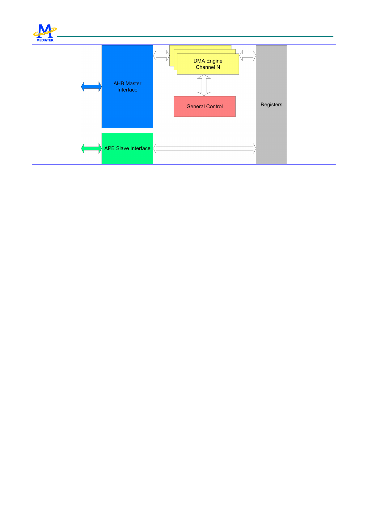
MT6225 GSM/GPRS Baseband Processor Data Sheet Revision 1.00
Figure 12 Block Diagram of Direct memory Access Module
3.4.1.1 Full-Size & Half-Size DMA Channels
There are three types of DMA channels in the DMA controller. The first one is called a full-size DMA channel, the
second one is called a half-size DMA channel, and the last is Virtual FIFO DMA. Channels 1 through 3 are full-size
DMA channels; channels 4 through 10 are half-size ones; and channels 11 through 14 are Virtual FIFO DMAs. The
difference between the first two types of DMA channels is that both source and destination address are programmable
in full-size DMA channels, but only the address of one side can be programmed in half-size DMA channel. In
half-size channels, only either the source or destination address can be programmed, while the addresses of the other
side is preset. Which preset address is used depends on the setting of MAS in DMA Channel Control Register.
Refer to the Register Definition section for more detail.
3.4.1.2 Ring Buffer & Double Buffer Memory Data Move
DMA channels 1 through 10 support ring-buffer and double-buffer memory data movement. This can be achieved by
programming DMA_WPPT and DMA_WPTO, as well as setting WPEN in DMA_CON register to enable. Figure 13
illustrates how this function works. Once the transfer counter reaches the value of WPPT, the next address jumps to
the WPTO address after completing the WPPT data transfer. Note that only one side can be configured as ring-buffer
or double-buffer memory, and this is controlled by WPSD in DMA_CON register.
ment
39
Page 40

MT6225 GSM/GPRS Baseband Processor Data Sheet Revision 1.00
Figure 14 Ring Buffer and Double Buffer Memory Data Movement
3.4.1.3 Unaligned Word Access
The address of word access on AHB bus must be aligned to word boundary, or the 2 LSB is truncated to 00b. If
programmers do not notice this, it may cause an incorrect data fetch. In the case where data is to be moved from
unaligned addresses to aligned addresses, the word is usually first split into four bytes and then moved byte by byte.
This results in four read and four write transfers on the bus.
To improve bus efficiency, unaligned-word access is provided in DMA4~10. While this function is enabled, DMAs
move data from unaligned address to aligned address by executing four continuous byte-read access and one
word-write access, reducing the number of transfers on the bus by three.
Figure 15 Unaligned Word Accesses
3.4.1.4 Virtual FIFO DMA
Virtual FIFO DMA is used to ease UART control. The difference between the Virtual FIFO DMAs and the ordinary
DMAs is that Virtual FIFO DMA contains additional FIFO controller. The read and write pointers are kept in the
Virtual FIFO DMA. During a read from the FIFO, the read pointer points to the address of the next data. During a
write to the FIFO, the write pointer moves to the next address. If the FIFO is empty, a FIFO read is not allowed.
Similarly, data is not written into the FIFO if the FIFO is full. Due to UART flow control requirements, an alert
40
Page 41
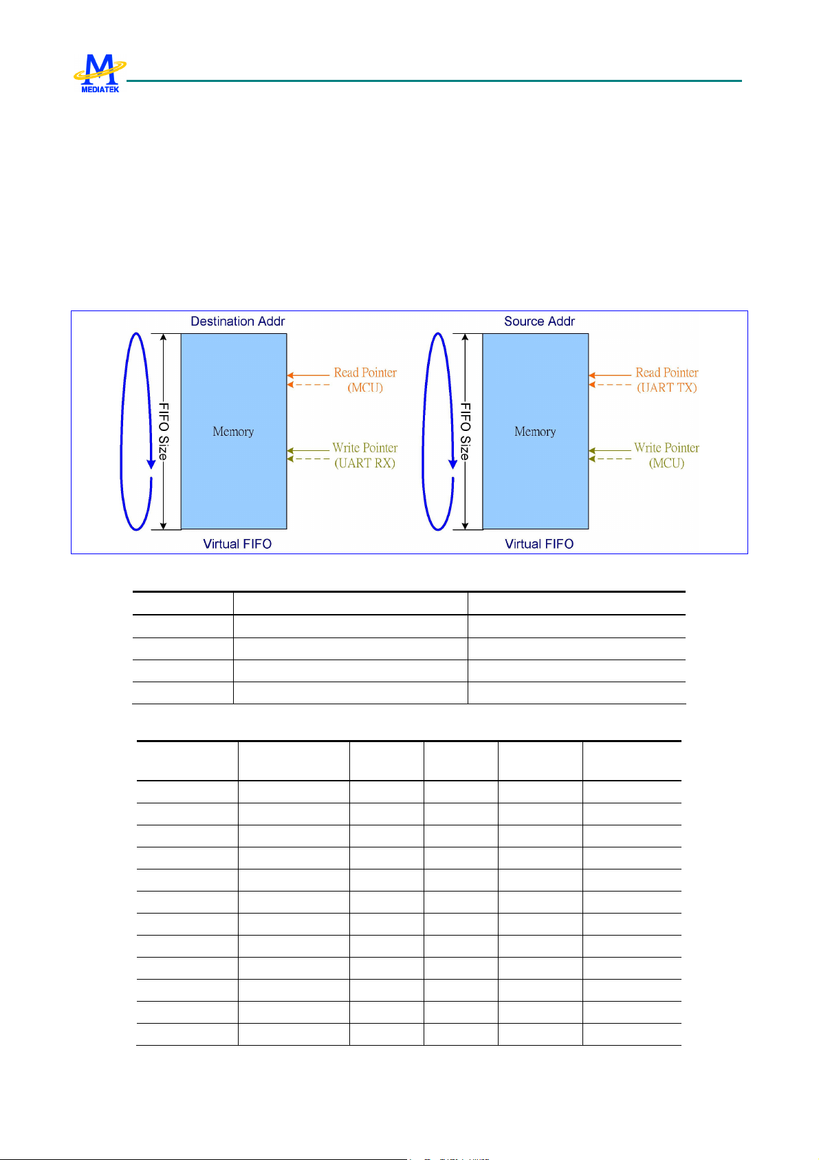
MT6225 GSM/GPRS Baseband Processor Data Sheet Revision 1.00
length is programmed. Once the FIFO Space is less than this value, an alert signal is issued to enable UART flow
control. The type of flow control performed depends on the setting in UART.
Each Virtual FIFO DMA can be programmed as RX or TX FIFO. This depends on the setting of DIR in DMA_CON
register. If DIR is “0”(READ), it means TX FIFO. On the other hand, if DIR is “1”(WRITE), the Virtual FIFO
DMA is specified as a RX FIFO.
Virtual FIFO DMA provides an interrupt to MCU. This interrupt informs MCU that there is data in the FIFO, and the
amount of data is over or under the value defined in DMA_COUNT register. With this, MCU does not need to poll
DMA to know when data must be removed from or put into the FIFO.
Note that Virtual FIFO DMAs cannot be used as generic DMAs, i.e. DMA1~10.
Figure 16 Virtual FIFO DMA
DMA number
DMA11 7800_0000h UART1 RX / ALL UART TX
DMA12 7800_0100h UART2 RX / ALL UART TX
DMA13 7800_0200h UART3 RX / ALL UART TX
DMA14 7800_0300h ALL UART TX
DMA number
DMA1 Full Size ● ● ●
DMA2 Full Size ● ● ●
DMA3 Full Size ● ● ●
DMA4 Half Size ● ● ● ●
DMA5 Half Size ● ● ● ●
DMA6 Half Size ● ● ● ●
DMA7 Half Size ● ● ● ●
DMA8 Half Size ● ● ● ●
DMA9 Half Size ● ● ● ●
DMA10 Half Size ● ● ● ●
DMA11 Virtual FIFO ●
DMA12 Virtual FIFO ●
Address of Virtual FIFO Access Port Associated UART
Table 7 Virtual FIFO Access Port
Type Ring Buffer Two Buffer Burst Mode
Unaligned Word
Access
41
Page 42

MT6225 GSM/GPRS Baseband Processor Data Sheet Revision 1.00
DMA13 Virtual FIFO ●
DMA14 Virtual FIFO ●
Table 8 Function List of DMA channels
REGISTER ADDRESS REGISTER NAME SYNONYM
DMA + 0000h DMA Global Status Register DMA_GLBSTA
DMA + 0028h DMA Global Bandwidth Limiter Register DMA_GLBLIMITER
DMA + 0100h DMA Channel 1 Source Address Register DMA1_SRC
DMA + 0104h DMA Channel 1 Destination Address Register DMA1_DST
DMA + 0108h DMA Channel 1 Wrap Point Address Register DMA1_WPPT
DMA + 010Ch DMA Channel 1 Wrap To Address Register DMA1_WPTO
DMA + 0110h DMA Channel 1 Transfer Count Register DMA1_COUNT
DMA + 0114h DMA Channel 1 Control Register DMA1_CON
DMA + 0118h DMA Channel 1 Start Register DMA1_START
DMA + 011Ch DMA Channel 1 Interrupt Status Register DMA1_INTSTA
DMA + 0120h DMA Channel 1 Interrupt Acknowledge Register DMA1_ACKINT
DMA + 0124h DMA Channel 1 Remaining Length of Current Transfer DMA1_RLCT
DMA + 0128h DMA Channel 1 Bandwidth Limiter Register DMA1_LIMITER
DMA + 0200h DMA Channel 2 Source Address Register DMA2_SRC
DMA + 0204h DMA Channel 2 Destination Address Register DMA2_DST
DMA + 0208h DMA Channel 2 Wrap Point Address Register DMA2_WPPT
DMA + 020Ch DMA Channel 2 Wrap To Address Register DMA2_WPTO
DMA + 0210h DMA Channel 2 Transfer Count Register DMA2_COUNT
DMA + 0214h DMA Channel 2 Control Register DMA2_CON
DMA + 0218h DMA Channel 2 Start Register DMA2_START
DMA + 021Ch DMA Channel 2 Interrupt Status Register DMA2_INTSTA
DMA + 0220h DMA Channel 2 Interrupt Acknowledge Register DMA2_ACKINT
DMA + 0224h DMA Channel 2 Remaining Length of Current Transfer DMA2_RLCT
DMA + 0228h DMA Channel 2 Bandwidth Limiter Register DMA2_LIMITER
DMA + 0300h DMA Channel 3 Source Address Register DMA3_SRC
DMA + 0304h DMA Channel 3 Destination Address Register DMA3_DST
DMA + 0308h DMA Channel 3 Wrap Point Address Register DMA3_WPPT
DMA + 030Ch DMA Channel 3 Wrap To Address Register DMA3_WPTO
DMA + 0310h DMA Channel 3 Transfer Count Register DMA3_COUNT
DMA + 0314h DMA Channel 3 Control Register DMA3_CON
DMA + 0318h DMA Channel 3 Start Register DMA3_START
DMA + 031Ch DMA Channel 3 Interrupt Status Register DMA3_INTSTA
DMA + 0320h DMA Channel 3 Interrupt Acknowledge Register DMA3_ACKINT
DMA + 0324h DMA Channel 3 Remaining Length of Current Transfer DMA3_RLCT
DMA + 0328h DMA Channel 3 Bandwidth Limiter Register DMA3_LIMITER
DMA + 0408h DMA Channel 4 Wrap Point Address Register DMA4_WPPT
DMA + 040Ch DMA Channel 4 Wrap To Address Register DMA4_WPTO
DMA + 0410h DMA Channel 4 Transfer Count Register DMA4_COUNT
42
Page 43

MT6225 GSM/GPRS Baseband Processor Data Sheet Revision 1.00
DMA + 0414h DMA Channel 4 Control Register DMA4_CON
DMA + 0418h DMA Channel 4 Start Register DMA4_START
DMA + 041Ch DMA Channel 4 Interrupt Status Register DMA4_INTSTA
DMA + 0420h DMA Channel 4 Interrupt Acknowledge Register DMA4_ACKINT
DMA + 0424h DMA Channel 4 Remaining Length of Current Transfer DMA4_RLCT
DMA + 0428h DMA Channel 4 Bandwidth Limiter Register DMA4_LIMITER
DMA + 042Ch DMA Channel 4 Programmable Address Register DMA4_PGMADDR
DMA + 0508h DMA Channel 5 Wrap Point Address Register DMA5_WPPT
DMA + 050Ch DMA Channel 5 Wrap To Address Register DMA5_WPTO
DMA + 0510h DMA Channel 5 Transfer Count Register DMA5_COUNT
DMA + 0514h DMA Channel 5 Control Register DMA5_CON
DMA + 0518h DMA Channel 5 Start Register DMA5_START
DMA + 051Ch DMA Channel 5 Interrupt Status Register DMA5_INTSTA
DMA + 0520h DMA Channel 5 Interrupt Acknowledge Register DMA5_ACKINT
DMA + 0524h DMA Channel 5 Remaining Length of Current Transfer DMA5_RLCT
DMA + 0528h DMA Channel 5 Bandwidth Limiter Register DMA5_LIMITER
DMA + 052Ch DMA Channel 5 Programmable Address Register DMA5_PGMADDR
DMA + 0608h DMA Channel 6 Wrap Point Address Register DMA6_WPPT
DMA + 060Ch DMA Channel 6 Wrap To Address Register DMA6_WPTO
DMA + 0610h DMA Channel 6 Transfer Count Register DMA6_COUNT
DMA + 0614h DMA Channel 6 Control Register DMA6_CON
DMA + 0618h DMA Channel 6 Start Register DMA6_START
DMA + 061Ch DMA Channel 6 Interrupt Status Register DMA6_INTSTA
DMA + 0620h DMA Channel 6 Interrupt Acknowledge Register DMA6_ACKINT
DMA + 0624h DMA Channel 6 Remaining Length of Current Transfer DMA6_RLCT
DMA + 0628h DMA Channel 6 Bandwidth Limiter Register DMA6_LIMITER
DMA + 062Ch DMA Channel 6 Programmable Address Register DMA6_PGMADDR
DMA + 0708h DMA Channel 7 Wrap Point Address Register DMA7_WPPT
DMA + 070Ch DMA Channel 7 Wrap To Address Register DMA7_WPTO
DMA + 0710h DMA Channel 7 Transfer Count Register DMA7_COUNT
DMA + 0714h DMA Channel 7 Control Register DMA7_CON
DMA + 0718h DMA Channel 7 Start Register DMA7_START
DMA + 071Ch DMA Channel 7 Interrupt Status Register DMA7_INTSTA
DMA + 0720h DMA Channel 7 Interrupt Acknowledge Register DMA7_ACKINT
DMA + 0724h DMA Channel 7 Remaining Length of Current Transfer DMA7_RLCT
DMA + 0728h DMA Channel 7 Bandwidth Limiter Register DMA7_LIMITER
DMA + 072Ch DMA Channel 7 Programmable Address Register DMA7_PGMADDR
DMA + 0808h DMA Channel 8 Wrap Point Address Register DMA8_WPPT
DMA + 080Ch DMA Channel 8 Wrap To Address Register DMA8_WPTO
DMA + 0810h DMA Channel 8 Transfer Count Register DMA8_COUNT
DMA + 0814h DMA Channel 8 Control Register DMA8_CON
DMA + 0818h DMA Channel 8 Start Register DMA8_START
DMA + 081Ch DMA Channel 8 Interrupt Status Register DMA8_INTSTA
43
Page 44

MT6225 GSM/GPRS Baseband Processor Data Sheet Revision 1.00
DMA + 0820h DMA Channel 8 Interrupt Acknowledge Register DMA8_ACKINT
DMA + 0824h DMA Channel 8 Remaining Length of Current Transfer DMA8_RLCT
DMA + 0828h DMA Channel 8 Bandwidth Limiter Register DMA8_LIMITER
DMA + 082Ch DMA Channel 8 Programmable Address Register DMA8_PGMADDR
DMA + 0908h DMA Channel 9 Wrap Point Address Register DMA9_WPPT
DMA + 090Ch DMA Channel 9 Wrap To Address Register DMA9_WPTO
DMA + 0910h DMA Channel 9 Transfer Count Register DMA9_COUNT
DMA + 0914h DMA Channel 9 Control Register DMA9_CON
DMA + 0918h DMA Channel 9 Start Register DMA9_START
DMA + 091Ch DMA Channel 9 Interrupt Status Register DMA9_INTSTA
DMA + 0920h DMA Channel 9 Interrupt Acknowledge Register DMA9_ACKINT
DMA + 0924h DMA Channel 9 Remaining Length of Current Transfer DMA9_RLCT
DMA + 0928h DMA Channel 9 Bandwidth Limiter Register DMA9_LIMITER
DMA + 092Ch DMA Channel 9 Programmable Address Register DMA9_PGMADDR
DMA + 0A08h DMA Channel 10 Wrap Point Address Register DMA10_WPPT
DMA + 0A0Ch DMA Channel 10 Wrap To Address Register DMA10_WPTO
DMA + 0A10h DMA Channel 10 Transfer Count Register DMA10_COUNT
DMA + 0A14h DMA Channel 10 Control Register DMA10_CON
DMA + 0A18h DMA Channel 10 Start Register DMA10_START
DMA + 0A1Ch DMA Channel 10 Interrupt Status Register DMA10_INTSTA
DMA + 0A20h DMA Channel 10 Interrupt Acknowledge Register DMA10_ACKINT
DMA + 0A24h
DMA Channel 10 Remaining Length of Current
Transfer
DMA10_RLCT
DMA + 0A28h DMA Channel 10 Bandwidth Limiter Register DMA10_LIMITER
DMA + 0A2Ch DMA Channel 10 Programmable Address Register DMA10_PGMADDR
DMA + 0B10h DMA Channel 11 Transfer Count Register DMA11_COUNT
DMA + 0B14h DMA Channel 11 Control Register DMA11_CON
DMA + 0B18h DMA Channel 11 Start Register DMA11_START
DMA + 0B1Ch DMA Channel 11 Interrupt Status Register DMA11_INTSTA
DMA + 0B20h DMA Channel 11 Interrupt Acknowledge Register DMA11_ACKINT
DMA + 0B28h DMA Channel 11 Bandwidth Limiter Register DMA11_LIMITER
DMA + 0B2Ch DMA Channel 11 Programmable Address Register DMA11_PGMADDR
DMA + 0B30h DMA Channel 11 Write Pointer DMA11_WRPTR
DMA + 0B34h DMA Channel 11 Read Pointer DMA11_RDPTR
DMA + 0B38h DMA Channel 11 FIFO Count DMA11_FFCNT
DMA + 0B3Ch DMA Channel 11 FIFO Status DMA11_FFSTA
DMA + 0B40h DMA Channel 11 Alert Length DMA11_ALTLEN
DMA + 0B44h DMA Channel 11 FIFO Size DMA11_FFSIZE
DMA + 0C10h DMA Channel 12 Transfer Count Register DMA12_COUNT
DMA + 0C14h DMA Channel 12 Control Register DMA12_CON
DMA + 0C18h DMA Channel 12 Start Register DMA12_START
DMA + 0C1Ch DMA Channel 12 Interrupt Status Register DMA12_INTSTA
DMA + 0C20h DMA Channel 12 Interrupt Acknowledge Register DMA12_ACKINT
44
Page 45

MT6225 GSM/GPRS Baseband Processor Data Sheet Revision 1.00
DMA + 0C28h DMA Channel 12 Bandwidth Limiter Register DMA12_LIMITER
DMA + 0C2Ch DMA Channel 12 Programmable Address Register DMA12_PGMADDR
DMA + 0C30h DMA Channel 12 Write Pointer DMA12_WRPTR
DMA + 0C34h DMA Channel 12 Read Pointer DMA12_RDPTR
DMA + 0C38h DMA Channel 12 FIFO Count DMA12_FFCNT
DMA + 0C3Ch DMA Channel 12 FIFO Status DMA12_FFSTA
DMA + 0C40h DMA Channel 12 Alert Length DMA12_ALTLEN
DMA + 0C44h DMA Channel 12 FIFO Size DMA12_FFSIZE
DMA + 0D10h DMA Channel 13 Transfer Count Register DMA13_COUNT
DMA + 0D14h DMA Channel 13 Control Register DMA13_CON
DMA + 0D18h DMA Channel 13 Start Register DMA13_START
DMA + 0D1Ch DMA Channel 13 Interrupt Status Register DMA13_INTSTA
DMA + 0D20h DMA Channel 13 Interrupt Acknowledge Register DMA13_ACKINT
DMA + 0D28h DMA Channel 13 Bandwidth Limiter Register DMA13_LIMITER
DMA + 0D2Ch DMA Channel 13 Programmable Address Register DMA13_PGMADDR
DMA + 0D30h DMA Channel 13 Write Pointer DMA13_WRPTR
DMA + 0D34h DMA Channel 13 Read Pointer DMA13_RDPTR
DMA + 0D38h DMA Channel 13 FIFO Count DMA13_FFCNT
DMA + 0D3Ch DMA Channel 13 FIFO Status DMA13_FFSTA
DMA + 0D40h DMA Channel 13 Alert Length DMA13_ALTLEN
DMA + 0D44h DMA Channel 13 FIFO Size DMA13_FFSIZE
DMA + 0E10h DMA Channel 14 Transfer Count Register DMA14_COUNT
DMA + 0E14h DMA Channel 14 Control Register DMA14_CON
DMA + 0E18h DMA Channel 14 Start Register DMA14_START
DMA + 0E1Ch DMA Channel 14 Interrupt Status Register DMA14_INTSTA
DMA + 0E20h DMA Channel 14 Interrupt Acknowledge Register DMA14_ACKINT
DMA + 0E28h DMA Channel 14 Bandwidth Limiter Register DMA14_LIMITER
DMA + 0E2Ch DMA Channel 14 Programmable Address Register DMA14_PGMADDR
DMA + 0E30h DMA Channel 14 Write Pointer DMA14_WRPTR
DMA + 0E34h DMA Channel 14 Read Pointer DMA14_RDPTR
DMA + 0E38h DMA Channel 14 FIFO Count DMA14_FFCNT
DMA + 0E3Ch DMA Channel 14 FIFO Status DMA14_FFSTA
DMA + 0E40h DMA Channel 14 Alert Length DMA14_ALTLEN
DMA + 0E44h DMA Channel 14 FIFO Size DMA14_FFSIZE
Table 9 DMA Controller Register Map
3.4.2 Register Definitions
Register programming tips:
Start registers shall be cleared, when associated ch
PGMADDR, i.e. programmable address, only exists in half-size DMA channels. If DIR in Control Register
is high, PGMADDR represents Destination Address. Conversely, If DIR in Control Register is low,
PGMADDR represents Source Address.
annels are being programmed.
45
Page 46

MT6225 GSM/GPRS Baseband Processor Data Sheet Revision 1.00
Functions of ring-buffer and double-buffer memory data movement can be activated on either source side or
destination side by programming DMA_WPPT & and DMA_WPTO, as well as setting WPEN in DMA_CON
register high. WPSD in DMA_CON register determines the activated side.
DMA+0000h DMA Global Status Register DMA_GLBSTA
Bit 31 30 29 28 27 26 25 24 23 22 21 20 19 18 17 16
Name IT14
Type RO RO RO RO RO RO RO RO RO RO RO RO
Reset 0 0 0 0 0 0 0 0 0 0 0 0
Bit 15 14 13 12 11 10 9 8 7 6 5 4 3 2 1 0
Name IT8 RUN8 IT7 RUN7 IT6 RUN6 IT5 RUN5 IT4 RUN4 IT3 RUN3 IT2 RUN2 IT1 RUN1
Type RO RO RO RO RO RO RO RO RO RO RO RO RO RO RO RO
Reset 0 0 0 0 0 0 0 0 0 0 0 0 0 0 0 0
RUN1
4
This register helps software program keep track of the global status of DMA channels.
RUNN DMA channel n status
0 Channel n is stopped or has completed the transfer
1 Channel n is currently running.
ITN Interrupt status for channel n
0 No interrupt is generated.
1 An interrupt is pending and waiting for service.
IT13
RUN1
3
RUN1
IT12
already.
2
1
RUN1
IT11
IT10
RUN1
0
IT9 RUN9
DMA+0028h DMA Global Bandwidth limiter Register
DMA_GLBLIMIT
ER
Bit 31 30 29 28 27 26 25 24 23 22 21 20 19 18 17 16
Name
Type
Reset
Bit 15 14 13 12 11 10 9 8 7 6 5 4 3 2 1 0
Name GLBLIMITER
Type WO
Reset 0
Please refer to the expression in DMAn_LIMITER for detailed note. The value of DMA_GLBLIMITER is set to all
DMA channels, from 1 to 14.
DMA+0n00h DMA Channel n Source Address Register DMAn
Bit 31 30 29 28 27 26 25 24 23 22 21 20 19 18 17 16
Name
Type
Reset
Bit 15 14 13 12 11 10 9 8 7 6 5 4 3 2 1 0
Name
Type
Reset
The above registers contain the base or current source address that the DMA channel is currently operating on.
Writing to this register specifies the base address of transfer source for a DMA channel. Before programming these
registers, the software program should make sure that STR in DMAn_START is set to 0; that is, the DMA channel is
stopped and disabled completely. Otherwise, the DMA channel may run out of order. Reading this register returns
the address value from which the DMA is reading.
SRC[31:16]
R/W
0
SRC[15:0]
R/W
0
_SRC
Note that n is from 1 to 3.
SRC S
RC[31:0] specifies the base or current address of transfer source for a DMA channel, i.e. channel 1, 2 or 3.
46
Page 47

MT6225 GSM/GPRS Baseband Processor Data Sheet Revision 1.00
WRITE Base address of transfer source
READ Address from which DMA is reading
DMA+0n04h DMA Channel n Destination Address Register DMAn_DST
Bit 31 30 29 28 27 26 25 24 23 22 21 20 19 18 17 16
Name
Type
Reset
Bit 15 14 13 12 11 10 9 8 7 6 5 4 3 2 1 0
Name
Type
Reset
The above registers contain the base or current destination address that the DMA channel is currently operating on..
Writing to this register specifies the base address of the transfer destination for a DMA channel. Before programming
these registers, the software should make sure that STR in DMAn_START is set to ‘0’; that is, the DMA channel is
stopped and disabled completely. Otherwise, the DMA channel may run out of order. Reading this register returns
the address value to which the DMA is writing.
Note that n is from 1 to 3.
DST[31:16]
R/W
0
DST[15:0]
R/W
0
DST D
ST[31:0] specifies the base or current address of transfer destination for a DMA channel, i.e. channel 1, 2 or
3.
WRITE Base address of transfer destination.
READ Address to which DMA is writing.
DMA+0n08h DMA Channel n Wrap Point Count Register DMAn_WPPT
Bit 31 30 29 28 27 26 25 24 23 22 21 20 19 18 17 16
Name
Type
Reset
Bit 15 14 13 12 11 10 9 8 7 6 5 4 3 2 1 0
Name
Type
Reset
The above registers are to specify the transfer count required to perform before the jump point. This can be used to
support ring buffer or double buffer style memory accesses. To enable this function, two control bits, WPEN and
WPSD, in DMA control register must be programmed. See the following register description for more details. If the
transfercounter in the DMA engine matches this value, an address jump occurs, and the next address is the address
specified in DMAn_WPTO. Before programming these registers, the software should make sure that STR in
DMAn_START is set to ‘0’, that is the DMA channel is stopped and disabled completely. Otherwise, the DMA
channel may run out of order. To enable this function, WPEN in DMA_CON is set.
Note that n is from 1 to 10.
WPPT[15:0]
R/W
0
WPPT WP
PT[15:0] specifies the amount of the transfer count from start to jumping point for a DMA channel, i.e.
channel 1 – 10.
WRITE Address of the jump point.
R
EAD Value set by the programmer.
DMA+0n0Ch DMA Channel n Wrap To Address Register DMAn_WPTO
Bit 31 30 29 28 27 26 25 24 23 22 21 20 19 18 17 16
Name
Type
Reset
WPTO[31:16]
R/W
0
47
Page 48
MT6225 GSM/GPRS Baseband Processor Data Sheet Revision 1.00
Bit 15 14 13 12 11 10 9 8 7 6 5 4 3 2 1 0
Name
Type
Reset
WPTO[15:0]
R/W
0
The above registers specify the address of the jump destination of a given DMA transfer to support ring buffer or
double buffer style memory accesses. To enable this function, set the two control bits, WPEN and WPSD, in the
DMA control register . See the following register description for more details. Before programming these registers,
the software should make sure that STR in DMAn_START is set to ‘0’, that is the DMA channel is stopped and
disabled completely. Otherwise, the DMA channel may run out of order. To enable this function, WPEN in
DMA_CON should be set.
Note that n is from 1 to 10.
WPTO WP
TO[31:0] specifies the address of the jump point for a DMA channel, i.e. channel 1 – 10.
WRITE Address of the jump destination.
READ Value set by the programmer.
DMA+0n10h DMA Channel n Transfer Count Register DMAn
Bit 31 30 29 28 27 26 25 24 23 22 21 20 19 18 17 16
Name
Type
Reset
Bit 15 14 13 12 11 10 9 8 7 6 5 4 3 2 1 0
Name
Type
Reset
LEN
R/W
0
_COUNT
This register specifies the amount of total transfer count that the DMA channel is required to perform. Upon
completion, the DMA channel generates an interrupt request to the processor while ITEN in DMAn_CON is set as ‘1’.
Note that the total size of data being transferred by a DMA channel is determined by LEN together with the SIZE in
DMAn_CON, i.e. LEN x SIZE.
For virtual FIFO DMA, this register is used to configure the RX threshold and TX threshold. Interrupt is triggered
while FIFO count >= RX threshold in RX path or FIFO count =< TX threshold in TX path. Note that ITEN bit in
DMA_CON register shall be set, or no interrupt is issued.
Note that n is from 1 to 14.
LEN The amount of total transfer count
DMA+0n14h DMA Channel n Control Register DMAn_CON
Bit 31 30 29 28 27 26 25 24 23 22 21 20 19 18 17 16
Name MAS DIR WPEN
Type R/W R/W R/W R/W
Reset 0 0 0 0
Bit 15 14 13 12 11 10 9 8 7 6 5 4 3 2 1 0
Name ITEN BURST B2W DRQ DINC SINC
Type R/W
Reset 0 0 0 0 0 0 0
R/W R/W R/W R/W R/W
This register contains all the available control schemes for a DMA channel that is ready for software programmer to
configure. Note that all these fields cannot be changed while DMA transfer is in progress or an unexpected situation
may occur.
Note that n is from 1 to 14.
SIZE Data size within the confine of a bus cycle per tra
nsfer.
48
WPS
D
SIZE
R/W
Page 49

MT6225 GSM/GPRS Baseband Processor Data Sheet Revision 1.00
These bits confines the data transfer size between source and destination to the specified value for individual
bus cycle. The size is in terms of byte and has maximum value of 4 bytes. It is mainly decided by the data
width of a DMA master.
00 Byte transfer/1 byte
01 Half-word transfer/2 bytes
10 Word transfer/4 bytes
11 Reserved
SINC Incremental source address. Source addresses incre
ase every transfer. If the setting of SIZE is Byte, Source
addresses increase by 1 every single transfer. If Half-Word, increase by 2; and if Word, increase by 4.
0 Disable
1 Enable
DINC Incremental destination address. Destination addresses increase every transfer. If the setting of SIZE is
Byte, Destination addresses increase by 1 every single transfer. If Half-Word, increase by 2; and Iif Word,
increase by 4.
0 Disable
1 Enable
DREQ Throttle and handshake control for DMA transfer
0 No throttle control during DMA transfer or transfer
s occurred only between memories
1 Hardware handshake management
The DMA master is able to throttle down the transfer rate by way of request-grant handshake.
B2W Word to Byte or Byte to Word transfer for the applications of transferring non-word-aligned-address data to
word-aligned-address data. Note that BURST is set to 4-beat burst while enabling this function, and the
SIZE is set to Byte.
N
O effect on channel 1 – 3 & 11 - 14.
0 Disable
1 Enable
BURST Transfer Type. Burst-type transfers have better bus efficiency. Mass data movement is recommended to use
this kind of transfer. However, note that burst-type transfer does not stop until all of the beats in a burst are
completed or transfer length is reached. FIFO threshold of peripherals must be configured carefully while
being used to move data from/to the peripherals.
What transfer type can be used is restricted by the SIZE. If SIZE is 00b, i.e. byte transfer, all of the four
transfer types can be used. If SIZE is 01b, i.e. half-word transfer, 16-beat incrementing burst cannot be used.
If SIZE is 10b, i.e. word transfer, only single and 4-beat incrementing burst
can be used.
NO effect on channel 11 - 14.
000 Single
001 Reserved
010 4-beat incrementing burst
011 Reserved
100 8-beat incrementing burst
101 Reserved
110 16-beat incrementing burst
111 Reserved
ITEN DMA transfer completion interrupt enable.
0 Disable
1 Enable
WPSD The side using address-wrapping function. Only one
side of a DMA channel can activate address-wrapping
function at a time.
N
O effect on channel 11 - 14.
49
Page 50

MT6225 GSM/GPRS Baseband Processor Data Sheet Revision 1.00
0 Address-wrapping on source .
1 Address-wrapping on destination.
WPEN Address-wrapping for ring buffer. The next address of DMA jumps to WRAP TO address when the current
address matches WRAP POINT count.
NO effect on channel 11 - 14.
0 Disable
1 Enable
DIR Directions of DMA transfer for half-size and Virtual
FIFO DMA channels, i.e. channels 4~14. The direction
is from the perspective of the DMA masters. WRITE means read from master and then write to the address
specified in DMA_PGMADDR, and vice versa.
NO effect on channel 1 - 3.
0 Read
1 Write
MAS Master selection. Specifies which master occupies this DMA channel. Once assigned to certain master, the
corresponding DREQ and DACK are connected. For half-size and Virtual FIFO DMA channels, i.e.
channels 4 ~ 14, a predefined address is assigned as well.
00000 SIM
00001 MSDC
00010 IrDA TX
00011 IrDA RX
00100 USB1 Write
00101 USB1 Read
00110 USB2 Write
00111 USB2 Read
01000 UART1 TX
01001 UART1 RX
01010 UART2 TX
01011 UART2 RX
01100 UART3 TX
01101 UART3 RX
01110 DSP-DMA
01111 NFI TX
10000 NFI RX
10001
I2C TX
10010 I2C RX
OTHERS Reserved
DMA+0n18h DMA Channel n Start Register DMAn_START
Bit 31 30 29 28 27 26 25 24 23 22 21 20 19 18 17 16
Name
Type
Reset
Bit 15 14 13 12 11 10 9 8 7 6 5 4 3 2 1 0
Name STR
Type R/W
Reset 0
This register controls the activity of a DMA channel. Note that prior to setting STR to “1”, all the configurations
should be done by giving proper value to the registers. Note also that once the STR is set to “1”, the hardware does
not clear it automatically no matter if the DMA channel accomplishes the DMA transfer or not. In other works, the
50
Page 51

MT6225 GSM/GPRS Baseband Processor Data Sheet Revision 1.00
value of STR stays “1” regardless of the completion of DMA transfer. Therefore, the software program should be
sure to clear STR to “0” before restarting another DMA transfer.
Note that n is from 1 to 14.
STR Start control for a DMA channel.
0 The DMA channel is stopped.
1 The DMA channel is started and running.
DMA+0n1Ch DMA Channel n Interrupt Status Register DM
Bit 31 30 29 28 27 26 25 24 23 22 21 20 19 18 17 16
Name
Type
Reset
Bit 15 14 13 12 11 10 9 8 7 6 5 4 3 2 1 0
Name INT
Type RO
Reset 0
An_INTSTA
This register shows the interrupt status of a DMA channel. It has the same value as DMA_GLBSTA.
Note that n is from 1 to 14.
INT Interrupt Status for DMA Channel
0 No interrupt request is generated.
1 One interrupt request is pending and waiting for service.
DMA+0n20h DMA Channel n Interrupt Acknowledge Register DMAn_ACKINT
Bit 31 30 29 28 27 26 25 24 23 22 21 20 19 18 17 16
Name
Type
Reset
Bit 15 14 13 12 11 10 9 8 7 6 5 4 3 2 1 0
Name ACK
Type WO
Reset 0
This register is used to acknowledge the current interrupt request associated with the completion event of a DMA
channel by software program. Note that this is a write-only register, and any read to it returns a value of “0”.
Note that n is from 1 to 14.
ACK Interrupt acknowledge for the DMA channel
0 No effect
1 Interrupt request is acknowledged and should be rel
inquished.
DMA Channel n Remaining Length of Current
DMA+0n24h
DMAn_RLCT
Transfer
Bit 31 30 29 28 27 26 25 24 23 22 21 20 19 18 17 16
Name
Type
Reset
Bit 15 14 13 12 11 10 9 8 7 6 5 4 3 2 1 0
Name
Type
Reset
This register is to reflect the left amount of the transfer.
Note that n is from 1 to 10.
RLCT
RO
0
51
Page 52

MT6225 GSM/GPRS Baseband Processor Data Sheet Revision 1.00
DMA+0n28h DMA Bandwidth limiter Register DMAn_LIMITER
Bit 31 30 29 28 27 26 25 24 23 22 21 20 19 18 17 16
Name
Type
Reset
Bit 15 14 13 12 11 10 9 8 7 6 5 4 3 2 1 0
Name LIMITER
Type R/W
Reset 0
This register is to suppress the Bus utilization of the DMA channel. The value is from 0 to 255. 0 means no
limitation, and 255 means totally banned. The value between 0 and 255 means certain DMA can have permission to
use AHB every (4 X n) AHB clock cycles.
Note that it is not recommended to limit the Bus utilization of the DMA channels because this increases the latency of
response to the masters, and the transfer rate decreases as well. Before using it, programmer must make sure that the
bus masters have some protective mechanism to avoid entering the wrong states.
Note that n is from 1 to 14.
LIMITER from 0 to 255. 0 means no limitation, 255 means tot
ally banned, and others mean Bus access permission
every (4 X n) AHB clock.
DMAn_PGMAD
DMA+0n2Ch DMA Channel n Programmable Address Register
DR
Bit 31 30 29 28 27 26 25 24 23 22 21 20 19 18 17 16
Name
Type
Reset
Bit 15 14 13 12 11 10 9 8 7 6 5 4 3 2 1 0
Name
Type
Reset
The above registers specify the address for a half-size DMA channel. This address represents a source address if DIR
in DMA_CON is set to 0, and represents a destination address if DIR in DMA_CON is set to 1. Before being able to
program these register, the software should make sure that STR in DMAn_START is set to ‘0’, that is the DMA channel
is stopped and disabled completely. Otherwise, the DMA channel may run out of order.
Note that n is from 4 to 14.
PGMADDR P
GMADDR[31:0] specifies the addresses for a half-size or a Virtual FIFO DMA channel, i.e. channel 4 –
14.
WRITE Address of the jump destination.
READ Current address of the transfer.
PGMADDR[31:16]
R/W
0
PGMADDR[15:0]
R/W
0
DMA+0n30h DMA Channel n Virtual FIFO Write Pointer Register DMAn_WRPTR
Bit 31 30 29 28 27 26 25 24 23 22 21 20 19 18 17 16
Name
Type
Bit 15 14 13 12 11 10 9 8 7 6 5 4 3 2 1 0
Name
Type
Note that n is from 11 to 14.
WRPTR Virtual FIFO Write Pointer.
WRPTR[31:16]
RO
WRPTR[15:0]
RO
52
Page 53

MT6225 GSM/GPRS Baseband Processor Data Sheet Revision 1.00
DMA+0n34h DMA Channel n Virtual FIFO Read Pointer Register DMAn_RDPTR
Bit 31 30 29 28 27 26 25 24 23 22 21 20 19 18 17 16
Name
Type
Bit 15 14 13 12 11 10 9 8 7 6 5 4 3 2 1 0
Name
Type
RDPTR[31:16]
RO
RDPTR[15:0]
RO
Note that n is from 11 to 14.
RDPTR Virtual FIFO Read Pointer.
DMA+0n38h DMA Channel n Virtual FIFO Data Count Register DMAn_FFCNT
Bit 31 30 29 28 27 26 25 24 23 22 21 20 19 18 17 16
Name
Type
Bit 15 14 13 12 11 10 9 8 7 6 5 4 3 2 1 0
Name
Type
Note that n is from 11 to 14.
FFCNT To display the number of data stored in FIFO. 0 means FIFO empty, and FIFO is full if FFCNT is equal to
FFSIZE.
FFCNT
RO
DMA+0n3Ch DMA Channel n Virtual FIFO Status Register DMAn_FFSTA
Bit 31 30 29 28 27 26 25 24 23 22 21 20 19 18 17 16
Name
Type
Reset
Bit 15 14 13 12 11 10 9 8 7 6 5 4 3 2 1 0
Name ALT
Type RO RO RO
Reset 0 1 0
Note that n is from 11 to 14.
FULL To indicate FIFO is full.
0 Not Full
1 Full
EMPTY To indicate FIFO is empty.
0 Not Empty
1 Empty
ALT To indicate FIFO Count is larger than ALTLEN. DMA i
ssues an alert signal to UART to enable UART flow
control.
0 Not reach alert region.
1 Reach alert region.
EMPT
Y
FULL
DMA+0n40h DMA Channel n Virtual FIFO Alert Length Re
Bit 31 30 29 28 27 26 25 24 23 22 21 20 19 18 17 16
Name
Type
Reset
Bit 15 14 13 12 11 10 9 8 7 6 5 4 3 2 1 0
Name ALTLEN
Type R/W
53
gister DMAn_ALTLEN
Page 54

MT6225 GSM/GPRS Baseband Processor Data Sheet Revision 1.00
Reset 0
Note that n is from 11 to 14.
ALTLEN Specifies the Alert Length of Virtual FIFO DMA. Once the remaining FIFO space is less than ALTLEN,
an alert signal is issued to UART to enable flow control. Normally, ALTLEN shall be larger than 16 for
UART application.
DMA+0n44h DMA Channel n Virtual FIFO Size Register DM
Bit 31 30 29 28 27 26 25 24 23 22 21 20 19 18 17 16
Name
Type
Reset
Bit 15 14 13 12 11 10 9 8 7 6 5 4 3 2 1 0
Name
Type
Reset
FFSIZE
R/W
0
An_FFSIZE
Note that n is from 11 to 14.
FFSIZE Specifies the FIFO Size of Virtual FIFO DMA.
3.5 Interrupt Controller
3.5.1 General Description
Figure 17 outlines the major functionality of the MCU Interrupt Controller. The interrupt controller processes all
interrupt sources coming from external lines and internal MCU peripherals. Since ARM7EJ-S core supports two
levels of interrupt latency, this controller generates two request signals: FIQ for fast, low latency interrupt request and
IRQ for more general interrupts with lower priority.
EINT FIQ
TDMA
GPT
SIM
UART1
KP
RTC
UART2
DSP2MCU
APB Bus
Interrupt
Input
Multiplex
Figure 18 Block Diagram of the Interrupt Controller
IRQ0
IRQ1
IRQ2
IRQn
IRQ31
SoftIRQ
Registers
FIQ
Controller
IRQ
Controller
IRQ
54
Page 55

MT6225 GSM/GPRS Baseband Processor Data Sheet Revision 1.00
One and only one of the interrupt sources can be assigned to FIQ Controller and have the highest priority in requesting
timing critical service. All the others share the same IRQ signal by connecting them to IRQ Controller. The IRQ
Controller manages up 32 interrupt lines of IRQ0 to IRQ31 with fixed priority in descending order.
The Interrupt Controller provides a simple software interface by mean of registers to manipulate the interrupt request
shared system. IRQ Selection Registers and FIQ Selection Register determine the source priority and connecting
relation among sources and interrupt lines. IRQ Source Status Register allows software program to identify the source
of interrupt that generates the interrupt request. IRQ Mask Register provides software to mask out undesired sources
some time. End of Interrupt Register permits software program to indicate to the controller that a certain interrupt
service routine has been finished.
Binary coded version of IRQ Source Status Register is also made available for software program to helpfully identify
the interrupt source. Note that while taking advantage of this, it should also take the binary coded version of End of
Interrupt Register coincidently.
One and only one of the interrupt sources can be assigned to FIQ Controller and have the highest priority in requesting
timing critical service. All the others should share the same IRQ signal by connecting them to IRQ Controller. The IRQ
Controller manages up 32 interrupt lines of IRQ0 to IRQ31 with fixed priority in descending order.
The Interrupt Controller provides a simple software interface by mean of registers to manipulate the interrupt request
shared system. IRQ Selection Registers and FIQ Selection Register determine the source priority and connecting
relation among sources and interrupt lines. IRQ Source Status Register allows software program to identify the source
of interrupt that generates the interrupt request. IRQ Mask Register provides software to mask out undesired sources
some time. End of Interrupt Register permits software program to indicate the controller that a certain interrupt service
routine has been finished.
Binary coded version of IRQ Source Status Register is also made available for software program to helpfully identify
the interrupt source. Note that while using this register, the controller also needs to use the corresponding binary coded
version of End of Interrupt Register for response.
The essential Interrupt Table of ARM7EJ-S core is shown as Table 10.
Address Description
00000000h System Reset
00000018h IRQ
0000001Ch FIQ
Table 11 Interrupt Table of ARM7EJ-S
3.5.1.1 Interrupt Source Masking
Interrupt controller provides the function of Interrupt Source Masking by the way of programming MASK register.
Any of them can be masked individually.
However, because of the bus latency, the masking takes effect no earlier than 3 clock cycles later. In this time, the
to-be-masked interrupts could come in and generate an IRQ pulse to MCU, and then disappear immediately. This
IRQ forces MCU going to Interrupt Service Routine and polling Status Register (IRQ_STA or IRQ_STA2), but the
register shows there is no interrupt. This might cause MCU malfunction.
There are two ways for programmer to protect their software.
1. Return from ISR (Interrupt Service Routine) immediately while the Status register shows no interrupt.
2. Set I bit of MCU before doing Interrupt Masking, and then clear it after Interrupt Masking done.
Both avoid the problem, but the first item recommended to have in the ISR.
55
Page 56

MT6225 GSM/GPRS Baseband Processor Data Sheet Revision 1.00
Interrupt controller provides the function of Interrupt Source Masking by the way of programming MASK register. Any
of them can be masked individually.
However, because of the bus latency, the masking takes effect a minimal of 3 clock cycles later. In this time, the
to-be-masked interrupts could come in and generate an IRQ pulse to MCU, and then disappear immediately. This IRQ
forces MCU to go into Interrupt Service Routine and poll the Status Register (IRQ_STA or IRQ_STA2), but the register
will show there is no interrupt. This may cause MCU malfunction.
There are two ways for programmers to protect their software.
1. Return from ISR (Interrupt Service Routine) immediately while the Status register shows no interrupt.
2. Set I bit of MCU before performing Interrupt Masking, and then clear it after Interrupt Masking done.
Both can avoid the problem, but it is always recommended to use the first method list above.
3.5.1.2 External Interrupt
This interrupt controller also integrates an Externa
coming from external sources, the EINT0~3, and 4 WakeUp interrupt requests, i.e. EINT4~7, coming from peripherals
used to inform system to resume the system clock.
The four external interrupts can be used for different kind of applications, mainly for event detections: detection of
hand free connection, detection of hood opening, detection of battery charger connection.
Since the external event may be unstable in a certain period, a de-bounce mechanism is introduced to ensure the
functionality. The circuitry is mainly used to verify that the input signal remains stable for a programmable number of
periods of the clock. When this condition is satisfied, for the appearance or the disappearance of the input, the output
of the de-bounce logic changes to the desired state. Note that, because it uses the 32 KHz slow clock for performing
the de-bounce process, the parameter of de-bounce period and de-bounce enable takes effect no sooner than one
32 KHz clock cycle (~31.25us) after the software program sets them. However, the polarities of EINTs are clocked
with the system clock. Any changes to them take effect immediately.
l Interrupt Controller that can support up to 4 interrupt requests
56
Page 57

MT6225 GSM/GPRS Baseband Processor Data Sheet Revision 1.00
Figure 19 Block diagram of External Interrupt Controller
REGISTER ADDRESS
REGISTER NAME SYNONYM
CIRQ + 0000h IRQ Selection 0 Register IRQ_SEL0
CIRQ + 0004h IRQ Selection 1 Register IRQ_SEL1
CIRQ + 0008h IRQ Selection 2 Register IRQ_SEL2
CIRQ + 000Ch IRQ Selection 3 Register IRQ_SEL3
CIRQ + 0010h IRQ Selection 4 Register IRQ_SEL4
CIRQ + 0014h IRQ Selection 5 Register IRQ_SEL5
CIRQ + 0018h FIQ Selection Register FIQ_SEL
CIRQ + 001Ch IRQ Mask Register IRQ_MASK
CIRQ + 0020h IRQ Mask Disable Register IRQ_MASK_DIS
CIRQ + 0024h IRQ Mask Enable Register IRQ_MASK_EN
CIRQ + 0028h IRQ Status Register IRQ_STA
CIRQ + 002Ch IRQ End of Interrupt Register IRQ_EOI
CIRQ + 0030h IRQ Sensitive Register IRQ_SENS
CIRQ + 0034h IRQ Software Interrupt Register IRQ_SOFT
CIRQ + 0038h FIQ Control Register FIQ_CON
CIRQ + 003Ch FIQ End of Interrupt Register FIQ_EOI
CIRQ + 0040h Binary Coded Value of IRQ_STATUS IRQ_STA2
CIRQ + 0044h Binary Coded Value of IRQ_EOI IRQ_EOI2
CIRQ + 0100h EINT Status Register EINT_STA
CIRQ + 0104h EINT Mask Register EINT_MASK
CIRQ + 0108h EINT Mask Disable Register EINT_MASK_DIS
57
Page 58

MT6225 GSM/GPRS Baseband Processor Data Sheet Revision 1.00
CIRQ + 010Ch EINT Mask Enable Register EINT_MASK_EN
CIRQ + 0110h EINT Interrupt Acknowledge Register EINT_INTACK
CIRQ + 0114h EINT Sensitive Register EINT_SENS
CIRQ + 0120h EINT0 De-bounce Control Register EINT0_CON
CIRQ + 0130h EINT1 De-bounce Control Register EINT1_CON
CIRQ + 0140h EINT2 De-bounce Control Register EINT2_CON
CIRQ + 0150h EINT3 De-bounce Control Register EINT3_CON
CIRQ + 0160h EINT4 De-bounce Control Register EINT4_CON
CIRQ + 0170h EINT5 De-bounce Control Register EINT5_CON
CIRQ + 0180h EINT6 De-bounce Control Register EINT6_CON
CIRQ + 0190h EINT7 De-bounce Control Register EINT7_CON
Table 12 Interrupt Controller Register Map
3.5.2 Register Definitions
C
IRQ+0000h IRQ Selection 0 Register IRQ_SEL0
Bit 31 30 29 28 27 26 25 24 23 22 21 20 19 18 17 16
Name IRQ5 IRQ4 IRQ3
Type R/W R/W R/W
Reset 5 4 3
Bit 15 14 13 12 11 10 9 8 7 6 5 4 3 2 1 0
Name IRQ2 IRQ1 IRQ0
Type R/W R/W R/W
Reset 2 1 0
CIRQ+0004h IRQ Selection 1 Register IRQ_SEL1
Bit 31 30 29 28 27 26 25 24 23 22 21 20 19 18 17 16
Name IRQB IRQA IRQ9
Type R/W R/W R/W
Reset B A 9
Bit 15 14 13 12 11 10 9 8 7 6 5 4 3 2 1 0
Name IRQ8 IRQ7 IRQ6
Type R/W R/W R/W
Reset 8 7 6
CIRQ+0008h IRQ Selection 2 Register IRQ_SEL2
Bit 31 30 29 28 27 26 25 24 23 22 21 20 19 18 17 16
Name IRQ11 IRQ10 IRQF
Type R/W R/W R/W
Reset 11 10 F
Bit 15 14 13 12 11 10 9 8 7 6 5 4 3 2 1 0
Name IRQE IRQD IRQC
Type R/W R/W R/W
Reset E D C
CIRQ+000Ch IRQ Selection 3 Register IRQ_SEL3
Bit 31 30 29 28 27 26 25 24 23 22 21 20 19 18 17 16
Name IRQ17 IRQ16 IRQ15
Type R/W R/W R/W
Reset 17 16 15
Bit 15 14 13 12 11 10 9 8 7 6 5 4 3 2 1 0
Name IRQ14 IRQ13 IRQ12
58
Page 59

MT6225 GSM/GPRS Baseband Processor Data Sheet Revision 1.00
Type R/W R/W R/W
Reset 14 13 12
CIRQ+0010h IRQ Selection 4 Register IRQ_SEL4
Bit 31 30 29 28 27 26 25 24 23 22 21 20 19 18 17 16
Name IRQ1D IRQ1C IRQ1B
Type R/W R/W R/W
Reset 1D 1C 1B
Bit 15 14 13 12 11 10 9 8 7 6 5 4 3 2 1 0
Name IRQ1A IRQ19 IRQ18
Type R/W R/W R/W
Reset 1A 19 18
CIRQ+0014h IRQ Selection 5 Register IRQ_SEL5
Bit 31 30 29 28 27 26 25 24 23 22 21 20 19 18 17 16
Name
Type
Reset
Bit 15 14 13 12 11 10 9 8 7 6 5 4 3 2 1 0
Name IRQ1F IRQ1E
Type R/W R/W
Reset 1F 1E
CIRQ+0018h FIQ Selection Register FIQ_SEL
Bit 31 30 29 28 27 26 25 24 23 22 21 20 19 18 17 16
Name
Type
Reset
Bit 15 14 13 12 11 10 9 8 7 6 5 4 3 2 1 0
Name FIQ
Type R/W
Reset 0
The IRQ/FIQ Selection Registers provide system designers with a flexible routing scheme to make various mappings of
priority among interrupt sources possible. It allows the interrupt sources to be mapped onto interrupt requests of either
FIQ or IRQ. While only one interrupt source can be assigned to FIQ, the other ones should share IRQ by mapping them
onto IRQ0 to IRQ1F, which are connected to IRQ controller. The priority of IRQ0-IRQ1F is fixed, i.e. IRQ0 > IRQ1 >
IRQ2 > … > IRQ1E > IRQ1F. During the software configuration process, the Interrupt Source Code of desired
interrupt source should be written into source field of the corresponding IRQ_SEL0-IRQ_SEL4/FIQ_SEL. 5-bit
Interrupt Source Codes for all interrupt sources are fixed and defined in Table 13. The IRQ/FIQ Selection Registers
provide system designers with a flexible routing scheme to make various mappings of priority among interrupt sources
possible. The registers allow the interrupt sources to be mapped onto interrupt requests of either FIQ or IRQ. While
only one interrupt source can be assigned to FIQ, the other ones share IRQs by mapping them onto IRQ0 to IRQ1F
connected to IRQ controller. The priority sequence of IRQ0~IRQ1F is fixed, i.e. IRQ0 > IRQ1 > IRQ2 > … > IRQ1E
> IRQ1F. During the software configuration process, the Interrupt Source Code of desired interrupt source should be
written into source field of the corresponding IRQ_SEL0-IRQ_SEL4/FIQ_SEL. Five-bit Interrupt Source Codes for
all interrupt sources are fixed and defined.
Interrupt Source STA2 (Hex)
STA
MFIQ 0 00000001
TDMA_CTIRQ1
TDMA_CTIRQ2
1 00000002
2 00000004
DSP2CPU 3 00000008
59
Page 60

MT6225 GSM/GPRS Baseband Processor Data Sheet Revision 1.00
SIM 4 00000010
DMA 5 00000020
TDMA 6 00000040
UART1 7 00000080
KeyPad 8 00000100
UART2 9 00000200
GPTimer A 00000400
EINT B 00000800
USB C 00001000
MSDC D 00002000
RTC E 00004000
IrDA F 00008000
LCD 10 00010000
UART3 11 00020000
MIRQ 12 00040000
WDT 13 00080000
NOT USED 14
Resizer 15 00200000
NFI 16 00400000
B2PSI 17 00800000
IRDBG 18 01000000
MSDC card detect
19 02000000
I2C 1a 04000000
NOT USED 1b
NOT USED 1c
NOT USED 1d
CAM 1e 40000000
Table 14 Interrupt Source Code for Interrupt Sources
FIQ, IRQ0-1F The 5-bit content of this field would be the Interr
upt Source Code shown in Table 15 indicating that
the certain interrupt source uses the associated interrupt line to generate fast interrupt requests. The 5-bit
content of this field corresponds to an Interrupt Source Code shown above.
CIRQ+001Ch IRQ Mask Register IRQ_MASK
Bit 31 30 29 28 27 26 25 24 23 22 21 20 19 18 17 16
Name IRQ1F IRQ1E
Type R/W R/W R/W R/W R/W R/W R/W R/W R/W R/W R/W R/W R/W R/W R/W R/W
Reset 1 1 1 1 1 1 1 1 1 1 1 1 1 1 1 1
Bit 15 14 13 12 11 10 9 8 7 6 5 4 3 2 1 0
Name IRQF IRQE IRQD IRQC IRQB IRQA IRQ9 IRQ8 IRQ7 IRQ6 IRQ5 IRQ4 IRQ3 IRQ2 IRQ1 IRQ0
Type R/W R/W R/W R/W R/W R/W R/W R/W R/W R/W R/W R/W R/W R/W R/W R/W
Reset 1 1 1 1 1 1 1 1 1 1 1 1 1 1 1 1
This register contains a mask bit for each interrupt line in IRQ Controller. The register allows each interrupt source
IRQ0 to IRQ1F to be disabled or masked separately under software control. After a system reset, all bit values are set
to 1 to indicate that interrupt requests are prohibited.
IRQ1D IRQ1C IRQ1B IRQ1
A
IRQ19 IRQ18 IRQ17 IRQ16 IRQ15 IRQ14 IRQ13 IRQ12 IRQ11 IRQ10
60
Page 61

MT6225 GSM/GPRS Baseband Processor Data Sheet Revision 1.00
This register contains mask bit for each interrupt line in IRQ Controller. It allows each interrupt source of IRQ0 to
IRQ1F to be disabled or masked out separately under software control. After System Reset, all bit values will be set to
‘1’ to indicate that interrupt requests are prohibited.
IRQ0-1F Mask control for the associated interrupt source in the IRQ controllerMask Control for the Associated
Interrupt Source in IRQ Controller
0 Interrupt is enabled
1 Interrupt is disabled
I
RQ_MASK_CL
CIRQ+0020h IRQ Mask Clear Register
Bit 31 30 29 28 27 26 25 24 23 22 21 20 19 18 17 16
Name IRQ1F IRQ1E
Type W1C W1C W1C W1C W1C W1C W1C W1C W1C W1C W1C W1C W1C W1C W1C W1C
Bit 15 14 13 12 11 10 9 8 7 6 5 4 3 2 1 0
Name IRQF IRQE IRQD IRQC IRQB IRQA IRQ9 IRQ8 IRQ7 IRQ6 IRQ5 IRQ4 IRQ3 IRQ2 IRQ1 IRQ0
Type W1C W1C W1C W1C W1C W1C W1C W1C W1C W1C W1C W1C W1C W1C W1C W1C
This register is used to clear bits in IRQ Mask Register. When writing to this register, the data bits that are HIGH
cause the corresponding bits in IRQ Mask Register to be cleared. Data bits that are LOW have no effect on the
corresponding bits in IRQ Mask Register.
IRQ1D IRQ1C IRQ1B IRQ1
A
IRQ19 IRQ18 IRQ17 IRQ16 IRQ15 IRQ14 IRQ13 IRQ12 IRQ11 IRQ10
R
This register is used to clear bits in the IRQ Mask Register. When writing to this register, the data bits that are high will
cause the corresponding bits in the IRQ Mask Register to be cleared. Data bits that are low have no effect on the
corresponding bits in the IRQ Mask Register
IRQ0-1F Clear corresponding bits in IRQ Mask Register.
0 nNo effect
1 Disable the corresponding MASK bit
I
RQ_MASK_SE
CIRQ+0024h IRQ Mask SET Register
Bit 31 30 29 28 27 26 25 24 23 22 21 20 19 18 17 16
Name IRQ1F IRQ1E
Type W1S W1S W1S W1S W1S W1S W1S W1S W1S W1S W1S W1S W1S W1S W1S W1S
Bit 15 14 13 12 11 10 9 8 7 6 5 4 3 2 1 0
Name IRQF IRQE IRQD IRQC IRQB IRQA IRQ9 IRQ8 IRQ7 IRQ6 IRQ5 IRQ4 IRQ3 IRQ2 IRQ1 IRQ0
Type W1S W1S W1S W1S W1S W1S W1S W1S W1S W1S W1S W1S W1S W1S W1S W1S
This register is used to set bits in the IRQ Mask Register. When writing to this register, the data bits that are HIGH
cause the corresponding bits in IRQ Mask Register to be set. Data bits that are LOW have no effect on the
corresponding bits in IRQ Mask Register.
This register is used to set bits in the IRQ Mask Register. When writing to this register, the data bits that are high will
cause the corresponding bits in the IRQ Mask Register to be set. Data bits that are low have no effect on the
corresponding bits in the IRQ Mask Register
IRQ1D IRQ1C IRQ1B IRQ1
A
IRQ19 IRQ18 IRQ17 IRQ16 IRQ15 IRQ14 IRQ13 IRQ12 IRQ11 IRQ10
T
IRQ0-1F Set corresponding bits in IRQ Mask Register.
0 nNo effect
1 Enable corresponding MASK bit
CIRQ+0028h IRQ Source Status Register IRQ_STA
Bit 31 30 29 28 27 26 25 24 23 22 21 20 19 18 17 16
61
Page 62
MT6225 GSM/GPRS Baseband Processor Data Sheet Revision 1.00
Name IRQ1F IRQ1E
Type RO RO RO RO RO RO RO RO RO RO RO RO RO RO RO RO
Reset 0 0 0 0 0 0 0 0 0 0 0 0 0 0 0 0
Bit 15 14 13 12 11 10 9 8 7 6 5 4 3 2 1 0
Name IRQF IRQE IRQD IRQC IRQB IRQA IRQ9 IRQ8 IRQ7 IRQ6 IRQ5 IRQ4 IRQ3 IRQ2 IRQ1 IRQ0
Type RO RO RO RO RO RO RO RO RO RO RO RO RO RO RO RO
Reset 0 0 0 0 0 0 0 0 0 0 0 0 0 0 0 0
IRQ1D IRQ1C IRQ1B IRQ1
A
IRQ19 IRQ18 IRQ17 IRQ16 IRQ15 IRQ14 IRQ13 IRQ12 IRQ11 IRQ10
This Register allows software to poll which interrupt line has generated an IRQ interrupt request. A bit set to 1
indicates a corresponding active interrupt line. Only one flag is active at a time. The IRQ_STA is type of read-clear;
write access has no effect on the content.
This Register allows software to poll which interrupt line generates the IRQ interrupt request. A bit set to ‘1’ indicates a
corresponding active interrupt line. Only one flag is active at a time. The IRQ_STA is type of READ-Clear, write
access will have no effect to the content.
IRQ0-1F Interrupt indicator for the associated interrupt source.Interrupt Indication for the Associated Interrupt
Source
0 The associated interrupt source is non-active.
1 The associated interrupt source is asserted.
CIRQ+002Ch IRQ End of Interrupt Register IRQ_EOI
Bit 31 30 29 28 27 26 25 24 23 22 21 20 19 18 17 16
Name IRQ1F IRQ1E
Type WO WO WO WO WO WO WO WO WO WO WO WO WO WO WO WO
Reset 0 0 0 0 0 0 0 0 0 0 0 0 0 0 0 0
Bit 15 14 13 12 11 10 9 8 7 6 5 4 3 2 1 0
Name IRQF IRQE IRQD IRQC IRQB IRQA IRQ9 IRQ8 IRQ7 IRQ6 IRQ5 IRQ4 IRQ3 IRQ2 IRQ1 IRQ0
Type WO WO WO WO WO WO WO WO WO WO WO WO WO WO WO WO
Reset 0 0 0 0 0 0 0 0 0 0 0 0 0 0 0 0
IRQ1D IRQ1C IRQ1B IRQ1
A
IRQ19 IRQ18 IRQ17 IRQ16 IRQ15 IRQ14 IRQ13 IRQ12 IRQ11 IRQ10
This register provides a mean for software to relinquish and to refresh the interrupt controller. Writing a 1 to a
specific bit position results in an End of Interrupt command issued internally to the corresponding interrupt line.
This register provides a mean for software to relinquish and refresh the Interrupt Controller. Writing a ‘1’ to the specific
bit position will result in an End of Interrupt Command internally to the corresponding interrupt line.
IRQ0-1F End of Interrupt command for the associated interru
pt line.End of Interrupt Command for the Associated
Interrupt Line
0 No service is currently in progress or pending
1 Interrupt request is in-service
CIRQ+0030h IRQ Sensitive Register IRQ_SENS
Bit 31 30 29 28 27 26 25 24 23 22 21 20 19 18 17 16
Name IRQ1F IRQ1E
Type R/W R/W R/W R/W R/W R/W R/W R/W R/W R/W R/W R/W R/W R/W R/W R/W
Reset 0 0 0 0 0 0 0 0 0 0 0 0 0 0 0 0
Bit 15 14 13 12 11 10 9 8 7 6 5 4 3 2 1 0
Name IRQF IRQE IRQD IRQC IRQB IRQA IRQ9 IRQ8 IRQ7 IRQ6 IRQ5 IRQ4 IRQ3 IRQ2 IRQ1 IRQ0
Type R/W R/W R/W R/W R/W R/W R/W R/W R/W R/W R/W R/W R/W R/W R/W R/W
Reset 0 0 0 0 0 0 0 0 0 0 0 0 0 0 0 0
All interrupt lines of IRQ Controller, IRQ0~IRQ1F can be programmed as either edge or level sensitive. By default,
all the interrupt lines are edge sensitive and should be active LOW. Once a interrupt line is programmed as edge
sensitive, an interrupt request is triggered only at the falling edge of interrupt line, and the next interrupt is not accepted
IRQ1D IRQ1C IRQ1B IRQ1
A
IRQ19 IRQ18 IRQ17 IRQ16 IRQ15 IRQ14 IRQ13 IRQ12 IRQ11 IRQ10
62
Page 63

MT6225 GSM/GPRS Baseband Processor Data Sheet Revision 1.00
until the EOI command is given. However, level sensitive interrupts trigger is according to the signal level of the
interrupt line. Once the interrupt line become from HIGH to LOW, an interrupt request is triggered, and another
interrupt request is triggered if the signal level remain LOW after an EOI command. Note that in edge sensitive mode,
even if the signal level remains LOW after EOI command, another interrupt request is not triggered. That is because
edge sensitive interrupt is only triggered at the falling edge.
All interrupt lines of IRQ Controller, IRQ0-IRQ1F can be programmed as either edge or level sensitive. By default, all
the interrupt lines are edge sensitive and should be active LOW. Once a interrupt line is programmed as edge sensitive,
an interrupt request is triggered only at the falling edge of interrupt line, and the next interrupt will not be taken until
the EOI command is given. However, level sensitive interrupt triggering is according to the signal level of the interrupt
line. Once the interrupt line become from High to Low, an interrupt request is triggered, and another interrupt request
will be triggered if the signal level remain Low after EOI command. Please note that in edge sensitive mode, even if the
signal level remains Low after EOI command, another interrupt request will not be triggered. This is because edge
sensitive interrupt is only triggered at the falling edge.
IRQ0-1F Sensitivity type of the associated Interrupt Source
Sensitive Type of the Associated Interrupt Source
0 Edge sensitivity with active LOW
1 Level sensitivity with active LOW
CIRQ+0034h IRQ Software Interrupt Register IRQ_SOFT
Bit 31 30 29 28 27 26 25 24 23 22 21 20 19 18 17 16
Name IRQ1F IRQ1E
Type R/W R/W R/W R/W R/W R/W R/W R/W R/W R/W R/W R/W R/W R/W R/W R/W
Reset 0 0 0 0 0 0 0 0 0 0 0 0 0 0 0 0
Bit 15 14 13 12 11 10 9 8 7 6 5 4 3 2 1 0
Name IRQF IRQE IRQD IRQC IRQB IRQA IRQ9 IRQ8 IRQ7 IRQ6 IRQ5 IRQ4 IRQ3 IRQ2 IRQ1 IRQ0
Type R/W R/W R/W R/W R/W R/W R/W R/W R/W R/W R/W R/W R/W R/W R/W R/W
Reset 0 0 0 0 0 0 0 0 0 0 0 0 0 0 0 0
IRQ1D IRQ1C IRQ1B IRQ1
A
IRQ19 IRQ18 IRQ17 IRQ16 IRQ15 IRQ14 IRQ13 IRQ12 IRQ11 IRQ10
Setting “1” to the specific bit position generates a software interrupt for corresponding iInterrupt Lline before mask.
This register is used for debug purpose.
IRQ0-IRQ1F Software Interrupt
CIRQ+0038h FIQ Control Register FIQ_CON
Bit 31 30 29 28 27 26 25 24 23 22 21 20 19 18 17 16
Name
Type
Reset
Bit 15 14 13 12 11 10 9 8 7 6 5 4 3 2 1 0
Name SENS
Type R/W R/W
Reset 0 1
MAS
K
This register provides a means for software program to control the FIQ cController.
MASK Mask cControl for the FIQ Interrupt Source
0 Interrupt is enabled
1 Interrupt is disabled
SENS Sensitivitye Ttype of the FIQ Interrupt Source
0 Edge sensitivity with active LOW
1 Level sensitivity with active LOW
63
Page 64

MT6225 GSM/GPRS Baseband Processor Data Sheet Revision 1.00
CIRQ+003Ch FIQ End of Interrupt Register FIQ_EOI
Bit 31 30 29 28 27 26 25 24 23 22 21 20 19 18 17 16
Name
Type
Reset
Bit 15 14 13 12 11 10 9 8 7 6 5 4 3 2 1 0
Name EOI
Type WO
Reset 0
This register provides a means for software to relinquish and to refresh the FIQ controller. Writing a ‘1’ to the specific
bit position results in an End of Interrupt command issued internally to the corresponding interrupt line.
This register provides a mean for software to relinquish and refresh the FIQ Controller. Writing a ‘1’ to the specific bit
position will result in an End of Interrupt Command internally to the corresponding interrupt line.
EOI End of Interrupt Ccommand
CIRQ+0040h Binary Coded Value of IRQ_STATUS IRQ_STA2
Bit 31 30 29 28 27 26 25 24 23 22 21 20 19 18 17 16
Name
Type
Reset
Bit 15 14 13 12 11 10 9 8 7 6 5 4 3 2 1 0
Name
Type RO
Reset 0 0
NOIR
Q
STAS
RO
This Register is a binary coded version of IRQ_STA. It is used by the software program to poll which interrupt line
has generated the IRQ interrupt request in a much easier way. Any read to it has the same result as reading IRQ_STA.
The IRQ_STA2 is also read-only; write access has no effect on the content. Note that IRQ_STA2 should be coupled
with IRQ_EOI2 while using it.
This Register is a binary coded version of IRQ_STA. It is used for software program to poll and see which interrupt
line generated the IRQ interrupt request in a much easier way. Any read to it has the same result as reading IRQ_STA.
The IRQ_STA2 is also READ-ONLY, write access has no effect to the content. Note that, IRQ_STA2 should be
coupled with IRQ_EOI2 while using it.
STSA Binary cCoded Vvalue of IRQ_STA
NOIRQ Indicating if there is an IRQ or not. If there is no
IRQ, this bit will beis highHIGH, and the value of STSA
should beis 0_0000b.
CIRQ+0044h Binary Coded Value of IRQ_EOI IRQ_EOI2
Bit 31 30 29 28 27 26 25 24 23 22 21 20 19 18 17 16
Name
Type
Reset
Bit 15 14 13 12 11 10 9 8 7 6 5 4 3 2 1 0
Name EOI
Type WO
Reset 0
This register is a binary coded version of IRQ_EOI. It provides an easier way for software program to relinquish and
to refresh the interrupt controller. Writing a specific code results in an End of Interrupt command issued internally to
the corresponding interrupt line. Note that IRQ_EOI2 should be coupled with IRQ_STA2 while using it.
64
Page 65

MT6225 GSM/GPRS Baseband Processor Data Sheet Revision 1.00
This register is a binary coded version of IRQ_EOI. It provides an easier way for software program to relinquish and
refresh the Interrupt Controller. Writing a specific code will result in an End of Interrupt Command internally to the
corresponding interrupt line. Note that, IRQ_EOI2 should be coupled with IRQ_STA2 while using it.
EOI Binary Ccoded Vvalue of IRQ_EOI
CIRQ+0100h EINT Interrupt Status Register EINT_STA
Bit 31 30 29 28 27 26 25 24 23 22 21 20 19 18 17 16
Name
Type
Reset
Bit 15 14 13 12 11 10 9 8 7 6 5 4 3 2 1 0
Name EINT7 EINT6 EINT5 EINT4 EINT3 EINT2 EINT1 EINT0
Type RO RO RO RO RO RO RO RO
Reset 0 0 0 0 0 0 0 0
This register keeps up with current status of which EINT Source generated the interrupt request. If EINT sources are
set to edge sensitive, EINT_IRQ will beis de-asserted while this register is read.
EINT0-EINT7 Interrupt Status
0 No Iinterrupt Rrequest is generated
1 Interrupt Rrequest is pending
CIRQ+0104h EINT Interrupt Mask Register EINT_MASK
Bit 31 30 29 28 27 26 25 24 23 22 21 20 19 18 17 16
Name
Type
Reset
Bit 15 14 13 12 11 10 9 8 7 6 5 4 3 2 1 0
Name EINT7 EINT6 EINT5 EINT4 EINT3 EINT2 EINT1 EINT0
Type R/W R/W R/W R/W R/W R/W R/W R/W
Reset 1 1 1 1 1 1 1 1
This register controls whether or not EINT Source is allowed to generate an interrupt request. Setting a “1”
to the specific bit position prohibits the external interrupt line from becoming active.
This register controls whether if EINT Source is allowed to generate interrupt request. Setting a “1” to the
specific bit position prohibits the External Interrupt Line to active accordingly.
EINT0-EINT7 Interrupt Mask
0 Interrupt rRequest is enabled.
1 Interrupt Rrequest is disabled.
E
INT_MASK_C
CIRQ+0108h EINT Interrupt Mask Clear Register
LR
Bit 31 30 29 28 27 26 25 24 23 22 21 20 19 18 17 16
Name
Type
Bit 15 14 13 12 11 10 9 8 7 6 5 4 3 2 1 0
Name EINT7 EINT6 EINT5 EINT4 EINT3 EINT2 EINT1 EINT0
Type W1C W1C W1C W1C W1C W1C W1C W1C
This register is used to clear individual mask bits. Only the bits set to 1 are in effect, and interrupt masks for which
the mask bit is set are cleared (set to 0). Otherwise the interrupt mask bit retains its original value.
This register is used to individually clear mask bit. Only the bits set to 1 are in effect, and these mask bits will set to 0.
Otherwise mask bits keep original value.
65
Page 66
MT6225 GSM/GPRS Baseband Processor Data Sheet Revision 1.00
EINT0-EINT7 Disable Mask mask for the aAssociated eExternal Iinterrupt sSource
0 Nno effect.
1 Disable the corresponding MASK bit.
CIRQ+010Ch EINT Interrupt Mask Set Register
EINT_MASK_S
ET
Bit 31 30 29 28 27 26 25 24 23 22 21 20 19 18 17 16
Name
Type
Bit 15 14 13 12 11 10 9 8 7 6 5 4 3 2 1 0
Name EINT7 EINT6 EINT5 EINT4 EINT3 EINT2 EINT1 EINT0
Type W1S W1S W1S W1S W1S W1S W1S W1S
This register is used to set individual mask bits. Only the bits set to 1 are in effect, and interrupt masks for which the
mask bit is set are set to 1. Otherwise the interrupt mask bit retains its original value.
This register is used to individually set mask bit. Only the bits set to 1 are in effect, and these mask bits will set to 1.
Otherwise mask bits keep original value.
EINT0-EINT7 Disable Mmask for the Aassociated Eexternal Iinterr
upt Ssource.
0 Nno effect.
1 Enable corresponding MASK bit.
CIRQ+0110h EINT Interrupt Acknowledge Register EINT_INTACK
Bit 31 30 29 28 27 26 25 24 23 22 21 20 19 18 17 16
Name
Type
Reset
Bit 15 14 13 12 11 10 9 8 7 6 5 4 3 2 1 0
Name EINT7 EINT6 EINT5 EINT4 EINT3 EINT2 EINT1 EINT0
Type WO WO WO WO WO WO WO WO
Reset 0 0 0 0 0 0 0 0
Writing “1” to the specific bit position acknowledge the interrupt request correspondingly to the external interrupt line
source.
Writing “1” to the specific bit position means to acknowledge the interrupt request correspondingly to the External
Interrupt Line source.
EINT0-EINT7 Interrupt aAcknowledgement
0 No effect.
1 Interrupt Request is acknowledged.
CIRQ+0114h EINT Sensitive Register EINT_SENS
Bit 31 30 29 28 27 26 25 24 23 22 21 20 19 18 17 16
Name
Type
Reset
Bit 15 14 13 12 11 10 9 8 7 6 5 4 3 2 1 0
Name EINT7 EINT6 EINT5 EINT4 EINT3 EINT2 EINT1 EINT0
Type R/W R/W R/W R/W R/W R/W R/W R/W
Reset 1 1 1 1 1 1 1 1
Sensitivity type of external interrupt source.
EINT0-7 Sensitive tType of the Aassociated Eexternal Iinterrupt sSource
0 Edge sensitivity.
1 Level sensitivity.
66
Page 67
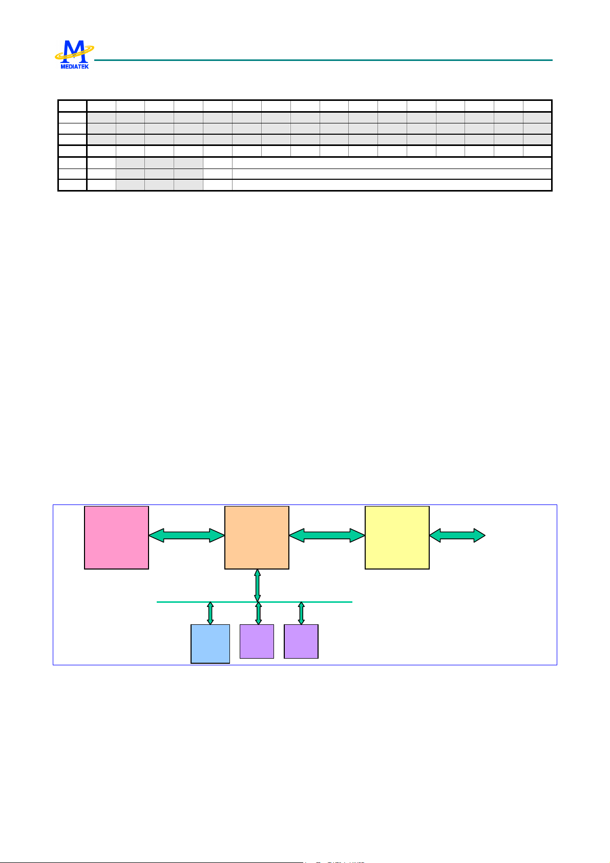
MT6225 GSM/GPRS Baseband Processor Data Sheet Revision 1.00
CIRQ+01m0h EINTn De-bounce Control Register EINTn_CON
Bit 31 30 29 28 27 26 25 24 23 22 21 20 19 18 17 16
Name
Type
Reset
Bit 15 14 13 12 11 10 9 8 7 6 5 4 3 2 1 0
Name EN
Type R/W
Reset 0 0 0
These registers control the de-bounce logic for external interrupt sources in order to minimize the possibility of false
activations.
These registers control the de-bounce logic for external interrupt sources in order to minimize the possibility of false
activations. EINT4 – 7 have no de-bounce mechanism. Therefore only bit POL is used.
Note that n is from 0 to 7, and m is n plus+ 2.
POL
R/W
CNT
R/W
CNT De-bounce Dduration in terms of numbers of 32KHz cl
POL Activation tType of the EINT sSource
0 Negative polarity
1 Positive polarity
EN De-bounce cControl Ccircuit
0 Disable
1 Enable
ock cycles
3.6 Code Cache controller
3
.6.1 General Description
A new subsystem consisting of cache and TCM (tightly coupled memory) will be implemented in MT6225. This
subsystem is placed between MCU core and AHB bus interface, as shown in Figure 20.
ARM7EJ
core
Cache
Controller
& MPU
AHB
bus
interface
AHB
TCM
Figure 20 Cache and TCM subsystem
TCM is a high-speed (zero wait state) dedicated memory accessed by MCU exclusively. Because MCU can run at
104MHz and on-chip bus runs at maximum 52MHz, there will be latency penalty when MCU accesses memory or
peripherals through on-chip bus. By moving timing critical code and data into TCM, MCU performance can be
increased and the response to particular events can be guaranteed.
Another method to increase MCU performance is the introduction of cache. Cache is a small memory, keeping the copy
of external memory. If MCU reads a cacheable data, the data will be copied to cache. Once MCU needs the same data
cache
way 0
cache
way 1
67
Page 68

MT6225 GSM/GPRS Baseband Processor Data Sheet Revision 1.00
72
KB
TCM
8 KB 8 KB
cache cache
72
KB
TCM
8 KB 8 KB
TCM cache
72
KB
TCM
8 KB 8 KB
TCM TCM
later, it can get it directly from cache (called cache hit) instead of from external memory, which takes long time
compared to high-speed (zero wait state) cache memory.
Since a large external memory maps to a small cache, cache can hold only a small portion of external memory. If MCU
accesses a data not found in cache (called cache miss), some contents of cache must be dropped (flushed) and the
required data is transferred from external memory (called cache line fill) and stored to cache. On the other hand, TCM
is not the copy of anything else. The best way to use TCM is to put critical code/data in TCM in the memory usage plan.
After power on reset, the boot loader copies TCM contents from external storage (such like flash) to internal TCM. If
necessary, MCU can replace a portion of TCM content with other data on external storage in the runtime to implement
a mechanism such like “overlay”. TCM is also an ideal place to put stack data.
The sizes of TCM and cache can be set to one of 3 configurations:
1 - way cache
Figure 21 Configurations of TCM and cache
72KB TCM, 16KB cache
2 - way cache
no cache
80KB TCM, 8KB cache
88KB TCM, 0KB cache
These configurations provide flexibility for software to adjust for optimum system performance.
The address mapping of these memories is like the following:
68
Page 69

MT6225 GSM/GPRS Baseband Processor Data Sheet Revision 1.00
No memory
cache
cache
cache
cache
TCM
TCM
8 K
8 K
8 K
8 K
72 K
K
cache
cache
cache
cache
TCM TCM
TCM TCM
adjacent
address.
holes.
cache
cache
TCM
TCM
TCM
TCM
TCM
TCM
TCM
TCM
Figure 22 Memory mapping of TCM and cache
In Figure 22, MCU could only access TCM explicitly. Cache is transparent to MCU.
3.6.2 Organization of Cache
The cache system has the following features:
Write through (no write allocation)
Configurable 1/2 way set associative (8K/16K)
Each way has 256 cache lines with 8 word line size (
19-bit tag address and 1 valid bit for each cache line.
One way of cache comprises of two memory: tag memory and data memory. Tag memory stores each line’s valid bit,
dirty bit and tag (upper part of address). Data memory stores line data. When MCU accesses memory, the address is
compared to the contents of tag memory. First the line index (address bit [12:5]) is used to locate a line, and then the tag
of the line is compared to upper part of address (bit [31:13]). If two parts match and valid bit is 1, it is said a cache hit
and data from that particular way is sent back to MCU. This process is illustrated in the following figure:
256*8*4=8KB)
69
Page 70
MT6225 GSM/GPRS Baseband Processor Data Sheet Revision 1.00
V T a g Da t
r
Da t
1 3 3 1 0
D
A dd r ess
512
4
Inde x
0
1
2
2 5 3
2 5 4
2 5 5
V T a g
D
D at a
1 9
8
a
2-t o-1 mult i p l ex o
H it
a
Figure 23 Tag comparison of 2-way cache
If most memory accesses are cache hit, MCU could get data immediately without wait states and the overall system
performance is higher. There are several factors that may affect cache hit rate:
Cache size and the organization
The larger the cache size is, the higher the hit rate is. But the hit rate starts to saturate when cache size is larger
than a threshold size. Normally the size of 16KB and above and two or four way can achieve a good hit rate.
Program behavior
I
f the system has several numbers of tasks that switch fast, it may cause cache contents to flush frequently.
Because each time a new task is run, the cache will hold its data after some time. If next task uses data in the
memory that occupy the same cache entries as previous task, it will cause cache contents to be flushed to store
data of the new task. Interrupts also cause program flow to change dynamically. The interrupt handler code
itself and the data it processes may cause cache to flush some data used by current task. Thus after exiting
interrupt handler and returning to current task, the flushed data may need to be filled to cache again, resulting
performance degradation.
To help software engineer tune system performance, the cache controller in MT6225 records the numbers of cache hit
count and cacheable memory accesses. Cache hit rate can be obtained from these two numbers.
The cache sub system also has a module called MPU (memory protection unit). MPU can prevent illegal memory
accesses and specify which memory region is cacheable or non-cacheable. Two fields in CACHE_CON register control
70
Page 71

MT6225 GSM/GPRS Baseband Processor Data Sheet Revision 1.00
the enable of MPU functions. MPU has its own registers to define memory region and associated regions. These
settings only take effect after the enable bits in CACHE_CON are set to 1. For more details on the settings, please refer
to MPU part of the specification.
3.6.3 Cache Operations
Upon power on, cache memory contains random numbers
and can’t be used by MCU. Therefore MCU must have some
means to “clean” cache memory before enabling them. Both above cases need a mechanism for MCU to perform
operations on cache. The cache controller provides a register which, when written, could do operations on cache
memory. These are called cache operations, including
Invalidate one cache line
The user must give a memory address. If it is found within cache, that particular line is invalidated (clear valid
bit to 0). Alternatively, the user can specify which set/way of cache to be invalidated.
Invalidate all cache lines
The user needs not to specify an address. The cache controller hardware automatically clears valid bits in each
tag memory.
3.6.4 Cache Controller Register Definition
CACHE base address is assumed 0x80700000 (subject to
CACHE+00h Cache General Control Register CACHE_CON
Bit 15 14 13 12 11 10 9 8 7 6 5 4 3 2 1 0
Name CACHESIZE
Type RW RW RW R/W R/W
Reset 00 0 0 0 0
change).
CNTE
N1
CNTE
N0
MPEN
MCE
N
This register determines the cache size, cache hit counter and the enable of MPU.
CACHESIZE Cache Size Select
00 no cache (88KB TCM)
01 8KB, 1-way cache (80KB TCM)
10 16KB, 2-way cache (72KB TCM)
C
NTEN1 Enable cache hit counter 1
If enabled, cache controller will increase a 48-bit counter each time a cache hit occurs. This number can
provide a reference of performance measurement for tuning of application programs. This counter increments
only when the cacheable information is from MPU cacheable region 4~7.
0 disable
1 enable
CNTEN0 Enable cache hit counter 0
If enabled, cache controller will increase a 48-bit counter each time a cache hit occurs. This number can
provide a reference of performance measurement for tuning of application programs. This counter increments
only when the cacheable information is from MPU cacheable region 0~3.
0 disable
1 enable
M
PEN Enable MPU comparison of read/write permission setting
If disabled, MCU could access any memory without any restriction. If enabled, MPU would compare the
address of MCU to its setting. If an address falls into a restricted region, MPU would stop this memory access
and send “ABORT” signal to MCU. Please refer to MPU part of the specification for more details.
71
Page 72

MT6225 GSM/GPRS Baseband Processor Data Sheet Revision 1.00
0 disable
1 enable
MCEN Enable MPU comparison of cacheable/non-cacheable setting
If disabled, MCU memory accesses are all non-cacheable, i.e., they will go through AHB bus (except for
TCM). If enabled, the setting in MPU will take effect. If MCU accesses a cacheable memory region, the cache
controller will return the data in cache if it’s found in cache, and will get the data through AHB bus only if a
cache miss occurs. Please refer to MPU part of the specification for more details.
0 disable
1 enable
CACHE+04h Cache Operation C
Bit 31 30 29 28 27 26 25 24 23 22 21 20 19 18 17 16
Name
Type
Reset
Bit 15 14 13 12 11 10 9 8 7 6 5 4 3 2 1 0
Name
Type
Reset
TADDR[15:5] OP[3:0] EN
R/W W W1
0 0 0
TADDR[31:16]
R/W
0
ACHE_OP
This register defines the address and/or which kinds of cache operations to be taken. When MCU writes this register,
the pipeline of MCU will be stopped for the cache controller to complete the operation. Bit 0 of the register must be
written 1 to enable the command.
TADDR[31:5] Target Address
This field contains the address of invalidation operation. If OP[3:0]=0010, TADDR[31:5] is the address[31:5]
of a memory whose line will be invalidated if it exists in the cache. If OP[3:0]=0100, TADDR[12:5] indicates
the set, while TADDR[19:16] indicates which way to clear:
0001 way #0
0
010 way #1
0100 way #2
1000 way #3
OP[3:0] Operation
This field determines which cache operations will be performed.
0001 invalidate all cache lines
0010 invalidate one cache line using address
0100 invalidate one cache line using set/way
EN Enable command
T
his enable bit must be written 1 to enable the command.
1 enable
0 not enable
CACHE+08h Cache Hit Count 0 Lower Part
Bit 31 30 29 28 27 26 25 24 23 22 21 20 19 18 17 16
Name
Type
Reset
Bit 15 14 13 12 11 10 9 8 7 6 5 4 3 2 1 0
Name
Type
Reset
CHIT_CNT0[31:16]
R/W
0
CHIT_CNT0[15:0]
R/W
0
72
L
CACHE_HCNT0
Page 73

MT6225 GSM/GPRS Baseband Processor Data Sheet Revision 1.00
CACHE+0Ch Cache Hit Count 0 Upper Part
Bit 31 30 29 28 27 26 25 24 23 22 21 20 19 18 17 16
Name
Type
Reset
Bit 15 14 13 12 11 10 9 8 7 6 5 4 3 2 1 0
Name
Type
Reset
When CNTEN0 bit in CACHE_CON register is set to 1 (enabled), this register starts to record cache hit count until it is
disabled. If the value increases to over maximum value (0xffffffffffff), it will be rolled over to 0 and continue counting.
The 48 bit counter can provide a recording time of 31 days even if MCU runs at 104MHz and every cycle is a cache hit.
Note that before enabling the counter, it is recommended to write the initial value of zero to the counter.
CHIT_CNT0[47:0] Cache Hit Count 0
WRITE writing any value to CACHE_HCNT0L or CACHE_HCNT0U cl
READ current counter value
RESERVED
CHIT_CNT0[47:32]
R/W
0
ears CHIT_CNT0 to all zeros
U
CACHE_CCNT0
CACHE_HCNT0
CACHE+10h Cacheable Access Count 0 Lower Part
Bit 31 30 29 28 27 26 25 24 23 22 21 20 19 18 17 16
Name
Type
Reset
Bit 15 14 13 12 11 10 9 8 7 6 5 4 3 2 1 0
Name
Type
Reset
CACC_CNT0[31:16]
R/W
0
CACC_CNT0[15:0]
R/W
0
L
CACHE+14h Cacheable Access Count 0 Upper Part
Bit 31 30 29 28 27 26 25 24 23 22 21 20 19 18 17 16
Name
Type
Reset
Bit 15 14 13 12 11 10 9 8 7 6 5 4 3 2 1 0
Name
Type
Reset
When CNTEN0 bit in CACHE_CON register is set to 1 (enabled), this register is incremented at each cacheable
memory access (no matter it’s a cache miss or a cache hit). If the value increases to over maximum value (0xffffffffffff),
it will be rolled over to 0 and continue counting. For 104MHz MCU speed, if all memory accesses are cacheable and
cache hit, this counter will overflow after (2^48) * 9.6ns = 31 days. This is the shortest time for the counter to overflow.
In a more realistic case, the system will have cache misses, non-cacheable accesses, idle mode that makes the counter
overflow at later time.
CACC_CNT0[47:0] Cache Access Count 0
WRITE writing any value to CACHE_CCNT0L or CACHE_CCNT0U cl
READ current counter value
RESERVED
CACC_CNT0[47:32]
R/W
0
ears CACC_CNT0 to all zeros
U
CACHE_CCNT0
73
Page 74
MT6225 GSM/GPRS Baseband Processor Data Sheet Revision 1.00
The best way to use CACHE_HCNT0 and CACHE_CCNT0 is to set zero as initial value in both registers, enable both
counters (set CNTEN0 to 1), run a portion of program to be benchmarked, stop the counters and get their values.
Therefore during this period
_
ratehitCache .
HCNTCACHE
_
CCNTCACHE
%100
×=
The cache hit rate value may help tune the performance of application program.
Note that CHIT_CNT0 and CACC_CNT0 only increment if the cacheable attribute is defined in MPU cacheable region
0~3.
C
CACHE+18h Cache Hit Count 1 Lower Part
Bit 31 30 29 28 27 26 25 24 23 22 21 20 19 18 17 16
Name
Type
Reset
Bit 15 14 13 12 11 10 9 8 7 6 5 4 3 2 1 0
Name
Type
Reset
CHIT_CNT1[31:16]
R/W
0
CHIT_CNT1[15:0]
R/W
0
ACHE_HCNT1
L
CACHE+1Ch Cache Hit Count 1 Upper Part
Bit 31 30 29 28 27 26 25 24 23 22 21 20 19 18 17 16
Name
Type
Reset
Bit 15 14 13 12 11 10 9 8 7 6 5 4 3 2 1 0
Name
Type
Reset
When CNTEN1 bit in CACHE_CON register is set to 1 (enabled), this register starts to record cache hit count until it is
disabled. If the value increases to over maximum value (0xffffffffffff), it will be rolled over to 0 and continue counting.
The 48 bit counter can provide a recording time of 31 days even if MCU runs at 104MHz and every cycle is a cache hit.
Note that before enabling the counter, it is recommended to write the initial value of zero to the counter.
CHIT_CNT1[47:0] Cache Hit Count
WRITE writing any value to CACHE_HCNT1L or CACHE_HCNT1U cl
READ current counter value
RESERVED
CHIT_CNT1[47:32]
R/W
0
ears CHIT_CNT1 to all zeros
U
CACHE_CCNT1
CACHE_HCNT1
CACHE+20h Cacheable Access Count 1 Lower Part
Bit 31 30 29 28 27 26 25 24 23 22 21 20 19 18 17 16
Name
Type
Reset
Bit 15 14 13 12 11 10 9 8 7 6 5 4 3 2 1 0
Name
Type
Reset
CACC_CNT1[31:16]
R/W
0
CACC_CNT1[15:0]
R/W
0
L
74
Page 75

MT6225 GSM/GPRS Baseband Processor Data Sheet Revision 1.00
CACHE+24h Cacheable Access Count 1 Upper Part
Bit 31 30 29 28 27 26 25 24 23 22 21 20 19 18 17 16
Name
Type
Reset
Bit 15 14 13 12 11 10 9 8 7 6 5 4 3 2 1 0
Name
Type
Reset
When CNTEN1 bit in CACHE_CON register is set to 1 (enabled), this register is incremented at each cacheable
memory access (no matter it’s a cache miss or a cache hit). If the value increases to over maximum value (0xffffffffffff),
it will be rolled over to 0 and continue counting. For 104MHz MCU speed, if all memory accesses are cacheable and
cache hit, this counter will overflow after (2^48) * 9.6ns = 31 days. This is the shortest time for the counter to overflow.
In a more realistic case, the system will have cache misses, non-cacheable accesses, idle mode that makes the counter
overflow at later time.
CACC_CNT1[47:0] Cache Access Count 1
WRITE writing any value to CACHE_CCNT1L or CACHE_CCNT1U cl
READ current counter value
The best way to use CACHE_HCNT1 and CACHE_CCNT1 is to set zero as initial value in both registers, enable both
counters (set CNTEN1 to 1), run a portion of program to be benchmarked, stop the counters and get their values.
Therefore during this period
RESERVED
CACC_CNT1[47:32]
R/W
0
ears CACC_CNT1 to all zeros
U
CACHE_CCNT1
_
ratehitCache .
The cache hit rate value may help tune the performance of application program.
Note that CHIT_CNT1 and CACC_CNT1 only increment if the cacheable attribute is defined in MPU cacheable region
4~7.
HCNTCACHE
_
CCNTCACHE
%100
×=
3.7 MPU
3.7.1 General Description
The purpose of MPU is to provide protection mechanis
MPU include
8-entry protection settings.
Determine if MCU can read/write a memory region. If the setting doesn’t allow MCU’s particular access to
a memory address, MPU will stop the memory access and issue “ABORT” signal to MCU, making it
entering into “abort” mode. The exception handler must then process the situation.
8-entry cacheable settings.
Determine a memory region is cacheable or not. If cacheable, MCU will keep a small copy in its cache after
read accesses. If MCU requires the same data later, it can get it from the high-speed local copy, instead of from
low-speed external memory.
m and cacheable indication of memory. The planned features of
Normally the protection and cacheable attributes are combined together for the same address range, as in the example
of ARM946E. For greater flexibility, the MPU in MT6225 provides independent protection and cacheable settings. That
75
Page 76
MT6225 GSM/GPRS Baseband Processor Data Sheet Revision 1.00
is to say, the memory regions defined for memory protection and for cacheable are different and independent of each
other.
The 4GB memory space is divided to 16 memory blocks of 256MB size, i.e., MB0~MB15. EMI takes MB0~MB3,
SYSRAM takes MB4, IDMA uses MB5, peripherals and other hardware take MB6~MB9, TCM (tightly-coupled
memory used by MCU exclusively) uses MB10. The characteristics of these memory blocks are listed below:
Read/write protection setting
MB5 and above (except MB10) are always readable/writeable.
MB0~MB4 and MB10 are determined by MPU.
Cacheable setting
MB4 and above are always non-cacheable.
MB0~MB3 are determined by MPU.
3.7.2 Protection Settings
MB10
MB9
~
MB6
MB5
MB4
MB3
~
MB0
TCM
Peripheral
IDMA
SYSRAM
EMI
Region 4
Region 4 base address
Region 3
Region 3 base address
Region 2
Region 2 base address
Region 1
Region 1 base address
Region 0
Region 0 base address
readable/writeable
non-readable/writeable
readable/non-writeable
non-readable/non-writeable
Figure 24 Protection setting
76
Page 77

MT6225 GSM/GPRS Baseband Processor Data Sheet Revision 1.00
1
Figure 24 shows the protection setting in each memory block. Five regions are defined in the figure. Note that each
region can be continuous or non-continuous to each other, and those address ranges not covered by any region are set to
be readable/writeable automatically. One restriction exists: different regions must not overlap.
The user can define maximum 8 regions in MB0~MB4 and MB10. Each region has its own setting defined in a 32-bit
register:
31 0
10
7 6
5
base address
Region base address (22 bits)
Region size (5 bits)
Region protection attribute (2 bits)
Enable bit (1 bit)
MPU will abort MCU if it accesses MB11~MB15 regions.
prot
00
size EN
3.7.2.1 Region base address
Region base address defines the start of the memory region. The user needs only to specify several upper address bits.
The number of valid address bits depends on the region size. The user must align the base address to a region-size
boundary. For example, if a region size is 8KB, its base address must be a multiple of 8KB.
3.7.2.2 Region size
The bit encoding of region size and its relationship
Region size Bit encoding Base address
1KB 00000 Bit [31:10] of region start address
2KB 00001 Bit [31:11] of region start address
4KB 00010 Bit [31:12] of region start address
8KB 00011 Bit [31:13] of region start address
16KB 00100 Bit [31:14] of region start address
32KB 00101 Bit [31:15] of region start address
64KB 00110 Bit [31:16] of region start address
128KB 00111 Bit [31:17] of region start address
256KB 01000 Bit [31:18] of region start address
512KB 01001 Bit [31:19] of region start address
1MB 01010 Bit [31:20] of region start address
2MB 01011 Bit [31:21] of region start address
4MB 01100 Bit [31:22] of region start address
8MB 01101 Bit [31:23] of region start address
16MB 01110 Bit [31:24] of region start address
with base address are listed as follows.
Table 16 Region size and bit encoding
3.7.2.3 Region protection attribute
This attribute has two bits. The MSB determines read access permission, and the LSB for write access permission.
Bit encoding Permission
77
Page 78
MT6225 GSM/GPRS Baseband Processor Data Sheet Revision 1.00
1
00 non-readable / non-writeable
10 readable / non-writeable
01 non-readable / writeable
11 readable / writeable
Table 17 Region protection attribute bit encoding
Note that bit encoding “11” allows full read/write permission, which is the case when no region is specified. So it is
recommended to only specify regions with protection attribute “00”, “10” or “01”.
3.7.3 Cacheable Settings
MB10
TCM
MB9
~
MB6
MB5
MB4
MB3
~
MB0
Figure 25 Cacheable setting
Peripheral
IDMA
SYSRAM
EMI
Region 2
Region 1
Region 0
uncacheable
c
acheable
Region 2 base address
Region 1 base address
Region 0 base address
Figure 25 shows the cacheable setting in each memory block. Three regions are defined in the figure. Note that each
region can be continuous or non-continuous to each other, and those address ranges not covered by any region are set to
be uncacheable automatically. One restriction exists: different regions must not overlap.
The user can define maximum 8 regions in MB0~MB3. Each region has its own setting defined in a 32-bit register:
31 0
base address
Region base address (22 bits)
Region size (5 bits)
Region cacheable attribute (1 bit)
78
10
000
C
5
6
size EN
Page 79

MT6225 GSM/GPRS Baseband Processor Data Sheet Revision 1.00
Enable bit (1 bit)
The region base address and region size bit encoding are the same as those of protection setting. The user must also
align the base address to a region-size boundary. The cacheable attribute has the following meaning.
Bit encoding Attribute
0 uncacheable
1 cacheable
Table 18 Region cacheable attribute bit encoding
3.7.4 MPU Register Definition
MPU base address is assumed 0x80701000 (subject to change).
MPU+0000h Protection setting for region 0 MPU_PROT0
Bit 31 30 29 28 27 26 25 24 23 22 21 20 19 18 17 16
Name
Type
Reset
Bit 15 14 13 12 11 10 9 8 7 6 5 4 3 2 1 0
Name
Type
Reset
BASEADDR[15:10] ATTR[1:0]
R W R W R W R W
11 00000 0
BASEADDR[31:16]
R W
SIZE[4:0] EN
This register sets protection attributes for region 0.
BASEADDR Base address of this region
ATTR Protection attribute
00 non-readable / non-writeable
01 n
on-readable / writeable
10 readable / non-writeable
11 readable / writeable
SIZE size of this region
00000 1KB
00001 2KB
00010 4KB
00011 8KB
00100 16KB
00101 32KB
00110 64KB
00111 128KB
01000 256KB
01001 512KB
01010 1MB
01011 2MB
01100 4MB
01101 8MB
01110 16MB
EN enable this region
0 Disable
1 Enable
79
Page 80

MT6225 GSM/GPRS Baseband Processor Data Sheet Revision 1.00
MPU+0004h Protection setting for region 1 MPU_PROT1
Bit 31 30 29 28 27 26 25 24 23 22 21 20 19 18 17 16
Name
Type
Reset
Bit 15 14 13 12 11 10 9 8 7 6 5 4 3 2 1 0
Name
Type
Reset
BASEADDR[15:10] ATTR[1:0]
R W R W R W R W
11 00000 0
BASEADDR[31:16]
R W
SIZE[4:0] EN
This register sets protection attributes for region 1.
MPU+0008h Protection setting for region 2 MPU_PROT2
Bit 31 30 29 28 27 26 25 24 23 22 21 20 19 18 17 16
Name
Type
Reset
Bit 15 14 13 12 11 10 9 8 7 6 5 4 3 2 1 0
Name
Type
Reset
BASEADDR[15:10] ATTR[1:0]
R W R W R W R W
11 00000 0
BASEADDR[31:16]
R W
SIZE[4:0] EN
This register sets protection attributes for region 2.
MPU+000Ch Protection setting for region 3 MPU_PROT3
Bit 31 30 29 28 27 26 25 24 23 22 21 20 19 18 17 16
Name
Type
Reset
Bit 15 14 13 12 11 10 9 8 7 6 5 4 3 2 1 0
Name
Type
Reset
BASEADDR[15:10] ATTR[1:0]
R W R W R W R W
11 00000 0
BASEADDR[31:16]
R W
SIZE[4:0] EN
This register sets protection attributes for region 3.
MPU+0010h Protection setting for region 4 MPU_PROT4
Bit 31 30 29 28 27 26 25 24 23 22 21 20 19 18 17 16
Name
Type
Reset
Bit 15 14 13 12 11 10 9 8 7 6 5 4 3 2 1 0
Name
Type
Reset
BASEADDR[15:10] ATTR[1:0]
R W R W R W R W
11 00000 0
This register sets protection attributes for region 4.
BASEADDR[31:16]
R W
SIZE[4:0] EN
MPU+0014h Protection setting for region 5 MPU_PROT5
Bit 31 30 29 28 27 26 25 24 23 22 21 20 19 18 17 16
Name
Type
Reset
Bit 15 14 13 12 11 10 9 8 7 6 5 4 3 2 1 0
Name
Type
Reset
BASEADDR[15:10] ATTR[1:0]
R W R W R W R W
11 00000 0
BASEADDR[31:16]
R W
SIZE[4:0] EN
80
Page 81

MT6225 GSM/GPRS Baseband Processor Data Sheet Revision 1.00
This register sets protection attributes for region 5.
MPU+0018h Protection setting for region 6 MPU_PROT6
Bit 31 30 29 28 27 26 25 24 23 22 21 20 19 18 17 16
Name
Type
Reset
Bit 15 14 13 12 11 10 9 8 7 6 5 4 3 2 1 0
Name
Type
Reset
BASEADDR[15:10] ATTR[1:0]
R W R W R W R W
11 00000 0
BASEADDR[31:16]
R W
SIZE[4:0] EN
This register sets protection attributes for region 6.
MPU+001Ch Protection setting for region 7 MPU_PROT7
Bit 31 30 29 28 27 26 25 24 23 22 21 20 19 18 17 16
Name
Type
Reset
Bit 15 14 13 12 11 10 9 8 7 6 5 4 3 2 1 0
Name
Type
Reset
BASEADDR[15:10] ATTR[1:0]
R W R W R W R W
11 00000 0
BASEADDR[31:16]
R W
SIZE[4:0] EN
This register sets protection attributes for region 7.
MPU+0040h Cacheable setting for region 0 MPU_CACHE0
Bit 31 30 29 28 27 26 25 24 23 22 21 20 19 18 17 16
Name
Type
Reset
Bit 15 14 13 12 11 10 9 8 7 6 5 4 3 2 1 0
Name
Type
Reset
BASEADDR[15:10] C SIZE[4:0] EN
R W R W
0 00000 0
This register sets cacheable attributes for region 0.
BASEADDR Base address of this region
C Cacheable attribute
0 u
ncacheable
1 cacheable
SIZE size of this region
00000 1KB
00001 2KB
00010 4KB
00011 8KB
00100 16KB
00101 32KB
00110 64KB
00111 128KB
01000 256KB
01001 512KB
01010 1MB
BASEADDR[31:16]
R W
R W R W
81
Page 82

MT6225 GSM/GPRS Baseband Processor Data Sheet Revision 1.00
01011 2MB
01100 4MB
01101 8MB
01110 16MB
EN enable this region
0 Disable
1 Enable
MPU+0044h Cacheable setting for region 1 MPU_CACHE1
Bit 31 30 29 28 27 26 25 24 23 22 21 20 19 18 17 16
Name
Type
Reset
Bit 15 14 13 12 11 10 9 8 7 6 5 4 3 2 1 0
Name
Type
Reset
BASEADDR[15:10] C SIZE[4:0] EN
R W R W
0 00000 0
BASEADDR[31:16]
R W
R W R W
This register sets cacheable attributes for region 1.
MPU+0048h Cacheable setting for region 2 MPU_CACHE2
Bit 31 30 29 28 27 26 25 24 23 22 21 20 19 18 17 16
Name
Type
Reset
Bit 15 14 13 12 11 10 9 8 7 6 5 4 3 2 1 0
Name
Type
Reset
BASEADDR[15:10] C SIZE[4:0] EN
R W R W
0 00000 0
BASEADDR[31:16]
R W
R W R W
This register sets cacheable attributes for region 2.
MPU+004Ch Cacheable setting for region 3 MPU_CACHE3
Bit 31 30 29 28 27 26 25 24 23 22 21 20 19 18 17 16
Name
Type
Reset
Bit 15 14 13 12 11 10 9 8 7 6 5 4 3 2 1 0
Name
Type
Reset
BASEADDR[15:10] C SIZE[4:0] EN
R W R W
0 00000 0
BASEADDR[31:16]
R W
R W R W
This register sets cacheable attributes for region 3.
MPU+0050h Cacheable setting for region 4 MPU_CACHE4
Bit 31 30 29 28 27 26 25 24 23 22 21 20 19 18 17 16
Name
Type
Reset
Bit 15 14 13 12 11 10 9 8 7 6 5 4 3 2 1 0
Name
Type
Reset
BASEADDR[15:10] C SIZE[4:0] EN
R W R W
0 00000 0
This register sets cacheable attributes for region 4.
BASEADDR[31:16]
R W
R W R W
82
Page 83

MT6225 GSM/GPRS Baseband Processor Data Sheet Revision 1.00
MPU+0054h Cacheable setting for region 5 MPU_CACHE5
Bit 31 30 29 28 27 26 25 24 23 22 21 20 19 18 17 16
Name
Type
Reset
Bit 15 14 13 12 11 10 9 8 7 6 5 4 3 2 1 0
Name
Type
Reset
BASEADDR[15:10] C SIZE[4:0] EN
R W R W
0 00000 0
BASEADDR[31:16]
R W
R W R W
This register sets cacheable attributes for region 5.
MPU+0058h Cacheable setting for region 6 MPU_CACHE6
Bit 31 30 29 28 27 26 25 24 23 22 21 20 19 18 17 16
Name
Type
Reset
Bit 15 14 13 12 11 10 9 8 7 6 5 4 3 2 1 0
Name
Type
Reset
BASEADDR[15:10] C SIZE[4:0] EN
R W R W
0 00000 0
BASEADDR[31:16]
R W
R W R W
This register sets cacheable attributes for region 6.
MPU+005Ch Cacheable setting for region 7 MPU_CACHE7
Bit 31 30 29 28 27 26 25 24 23 22 21 20 19 18 17 16
Name
Type
Reset
Bit 15 14 13 12 11 10 9 8 7 6 5 4 3 2 1 0
Name
Type
Reset
BASEADDR[15:10] C SIZE[4:0] EN
R W R W
0 00000 0
BASEADDR[31:16]
R W
R W R W
This register sets cacheable attributes for region 7.
3.8 Internal Memory Interface
3
.8.1 System RAM
MT6225 provides one 72K Bytes size of on-chip memory modules acting as System RAM for data access with low
latency. Such a module is composed of one high speed synchronous SRAM with AHB Slave Interface connected to the
system backbone AHB Bus, as shown in Figure 26. The synchronous SRAM operates on the same clock as the AHB
Bus and is organized as 32 bits wide with 4 byte-write signals capable for byte operations. The SRAM macro has
limited repair capability. The yield of SRAM is improved if the defects inside it can be repaired during testing.
3.8.2 System ROM
The 15K Bytes System ROM is primarily used to store
routines. This module is composed of high-speed ROM with an AHB Slave Interface connected to a system backbone
AHB, shown in Figure 26. The module operates on the same clock as the AHB and has a 32-bit wide organization.
software program for Factory Programming and security-related
83
Page 84

MT6225 GSM/GPRS Baseband Processor Data Sheet Revision 1.00
Graphsys
AHB Bus 0
Graphsys
AHB Bus 0
MCU AHB Bus
MCU AHB Bus
DMA AHB Bus
LCD AHB Bus
Figure 26: Block Diagram of the Internal Memory Controller
3.9 External Memory Interface
3
.9.1 General Description
Bank0 SRAM
Bank0 SRAM
ROM
ROM
MT6225 incorporates a powerful and flexible memory controller, External Memory Interface, to connect with a variety
of memory components. This controller provides one generic access scheme for Flash Memory, SRAM, PSRAM and
CellularRAM and another access scheme for MobileRAM. Up to 3 memory banks can be supported simultaneously,
BANK0-BANK2, with a maximum size of 64MB each.
Since most of the Flash Memory, SRAM, PSRAM and CellularRAM have similar AC requirements, a generic
configuration scheme to interface them is desired. This way, the software program can treat different components by
simply specifying certain predefined parameters. All these parameters are based on the cycle time of system clock.
The interface definition based on such a scheme is listed in Table 19. Note that, this interface always works with data
in Little Endian format for all types of access.
Signal Name Type Description
EA[25:0] O Address Bus
ED[15:0] I/O Data Bus
EWR# O Write Enable Strobe/MobileRAM Command Input
ERD# O Read Enable Strobe
ELB# O Lower Byte Strobe/MobileRAM Data Input & Output Mask
EUB# O Upper Byte Strobe/MobileRAM Data Input & Output Mask
ECS[3:0]# O BANK0~BANK3 Selection Signal
EPDN O PSRAM Power Down Control Signal
ECLK O Flash, SRAM, PSRAM and CellularRAM Clock Signal
EADV# O Flash, SRAM, PSRAM and CellularRAM Address Valid Signal
EWAIT I Flash, SRAM, PSRAM and CellularRAM Wait Signal Input
EDCLK O MobileRAM Clock Signal
ECKE O MobileRAM Clock Enable Signal
ERAS# O MobileRAM Row Address Signal
ECAS# O MobileRAM Column Address Signal
Table 19 External Memory Interface Signal of MT6225
84
Page 85

MT6225 GSM/GPRS Baseband Processor Data Sheet Revision 1.00
REGISTER ADDRESS REGISTER NAME SYNONYM
EMI + 0000h EMI Control Register for BANK0 EMI_CONA
EMI + 0008h EMI Control Register for BANK1 EMI_CONB
EMI + 0010h EMI Control Register for BANK2 EMI_CONC
EMI + 0040h EMI Control Register 0 for MobileRAM EMI_CONI
EMI + 0048h EMI Control Register 1 for MobileRAM EMI_CONJ
EMI + 0050h EMI Control Register 2 for MobileRAM EMI_CONK
EMI + 0058h EMI Control Register 3 for MobileRAM EMI_CONL
EMI + 0060h EMI Remap Control Register EMI_REMAP
EMI + 0068h EMI General Control Register 0 EMI_GENA
EMI + 0070h EMI General Control Register 1 EMI_GENB
Table 20 External Memory Interface Register Map
3.9.2 Register Definitions
EMI+0000h EMI Control Register for BANK 0 EMI_CONA
Bit 31 30 29 28 27 26 25 24 23 22 21 20 19 18 17 16
Name
Type
Reset
Bit 15 14 13 12 11 10 9 8 7 6 5 4 3 2 1 0
Name DW RBLN BW
Type R/W R/W R/W
Reset 0 1 0 0 0 0 7
C2WS C2WH C2RS PRLT
R/W R/W R/W R/W R/W R/W
0 0 0 0 0 0
WST WAIT PSIZE RLT
R/W R/W R/W R/W
CLKEN PMO
DE
EMI+0008h EMI Control Register for BANK 1 EMI_CONB
Bit 31 30 29 28 27 26 25 24 23 22 21 20 19 18 17 16
Name
Type
Reset
Bit 15 14 13 12 11 10 9 8 7 6 5 4 3 2 1 0
Name DW RBLN BW
Type R/W R/W R/W
Reset 0 1 0 0 0 0 7
C2WS C2WH C2RS PRLT
R/W R/W R/W R/W R/W R/W
0 0 0 0 0 0
WST WAIT PSIZE RLT
R/W R/W R/W R/W
CLKEN PMO
DE
EMI+0010h EMI Control Register for BANK 2 EMI_CONC
Bit 31 30 29 28 27 26 25 24 23 22 21 20 19 18 17 16
Name
Type
Reset
Bit 15 14 13 12 11 10 9 8 7 6 5 4 3 2 1 0
Name DW RBLN BW
Type R/W R/W R/W
Reset 0 1 0 0 0 0 7
C2WS C2WH C2RS PRLT
R/W R/W R/W R/W R/W R/W
0 0 0 0 0 0
WST WAIT PSIZE RLT
R/W R/W R/W R/W
CLKEN PMO
DE
For each bank (BANK0-BANK2), a dedicated control register is associated with the bank controller. These registers
have timing parameters that help the controller to convert memory access into proper timing waveform. Note that,
85
Page 86

MT6225 GSM/GPRS Baseband Processor Data Sheet Revision 1.00
ECLK
RLT+1
EA
ECS#
C2RS
ERD#
ED
ELB#/EUB#
EADV#
RLT=4, C2RS=1
ECLK
RLT+1
EA
ECS#
C2RS
ERD#
ED
ELB#/EUB#
EADV#
EWAIT
RLT=1, C2RS=1, WAIT=1
except for parameters CLKEN, PMODE, DW, RBLN, BW, WAIT and PSIZE, all the other parameters specified
explicitly are based on system clock speed in terms of cycle count.
RLT Read Latency Time
Specifies the number of wait-states to insert in the bus transfer to the requesting agent. Such a parameter
must be chosen carefully to meet the timing specification requirements for common parameter tACC(address
access time) for asynchronous-read device and tCWT(chip select low to wait valid time) for synchronous-read
device. An example is shown below.
Figure 27 Read Wait State Timing Diagram for Asynchronous-Read Memory (CLKEN=0)
Access Time Read Latency Time in 104 MHz unit
65 ns ~ 70 ns 7
85 ns ~ 90 ns 9
110 ns ~ 120 ns 12
Table 21 Reference value of Read Latency Time for Asynchronous-Read memory Devices
Figure 28 Read Wait State Timing Diagram for Synchronous-Read Memory (CLKEN=1)
ECS# Low to EWAIT Valid Read Latency Time in 104 MHz unit
0 ns ~ 10 ns 1
10 ns ~ 20 ns 2
Table 22 Reference value of Read Latency Time for Synchronous-Read Devices
86
Page 87

MT6225 GSM/GPRS Baseband Processor Data Sheet Revision 1.00
ECLK
WST+C2WH+2
EA
ECS#
C2WS
C2WH+1
EWR#
ED
ELB#/EUB#
EADV#
WST=3, C2WS=1, C2WH=0
ECLK
WST+1
EA
ECS#
EWR#
ED
ELB#/EUB#
EADV#
EWAIT
WST=1, C2WS=0, WAIT=1
PSIZE This bit position describes the page size behavior of that the Page Mode enabled device.
0 8 byte, EA[22:3] remains the same
1 16 byte, EA[22:4] remains the same
WAIT Data-valid feedback operation control for Flash memory, PSRAM and CellularRAM.
0 Disable data-valid feedback operation control
1 Enable data-valid feedback operation control
WST Write Wait State
Specifies the parameters to extend adequate setup and hold time for target component in write operation.
Such parameter must be chosen carefully to meet the timing specification requirements for common parameter
tWC(write cycle time) for asynchronous-write device and tCWT(chip select low to wait valid time) for
synchronous-write device. An example is shown in Figure 29 and Table 23.
Figure 29 Write Wait State Timing Diagram for Asynchronous-Write Memory (BW=0)
Write Pulse Width
(Write Data Setup Time)
Write Wait State in 104 MHz unit
65 ns ~ 70 ns 7
85 ns ~ 90 ns 9
110 ns ~ 120 ns 12
Table 23 Reference value of Write Wait State for Asynchronous-Write Devices
Figure 30 Write Wait State Timing Diagram for Synchronous-Write Memory (CLKEN=1 and BW=1)
ECS# Low to EWAIT Valid Write Wait State in 104 MHz unit
0 ns ~ 10 ns 1
87
Page 88

MT6225 GSM/GPRS Baseband Processor Data Sheet Revision 1.00
10 ns ~ 20 ns 2
Table 24 Reference value of Write Wait State for Synchronous-Write Devices
BW Burst Mode Write Control
0 Disable burst write operation
1 Enable burst write operation
RBLN Read Byte Lane Enable
DW Data Width
0 16 Bit
1 8 Bit
PMODE Page Mode Control
If the target device supports page mode operations, the Page Mode Control can be enabled. Read in Page
Mode is determined by the set of parameters: PRLT and PSIZE.
0 disable page mode operation
1 e
nable page mode operation
PRLT Read Latency Time within the Same Page
Since page mode operation only helps to eliminate read latency in subsequent access within the same page, the
initial latency does not matter. Thus, the memory controller must still adopt the RLT parameter for the initial
read or reads between different pages, even if PMODE is set to 1.
CLKEN Clock Enable Control
C2RS Chip Select to Read Strobe Setup Time
C2WH Chip Select to Write Strobe Hold Time
C2WS Chip Select to Write Strobe Setup Time
EMI+0040h EMI Control Register 0 for MobileRAM EMI_C
Bit 31 30 29 28 27 26 25 24 23 22 21 20 19 18 17 16
E_EN
PING
PONG
_EN
DRAM_MOD
E
R/W R/W R/W
DRAM_SIZE
DRAM
_EN
DRAM_CS
R/W
Name
Type R/W R/W
Reset 0 0 2d 0 0 0
Bit 15 14 13 12 11 10 9 8 7 6 5 4 3 2 1 0
Name BA1 BA0 A12 A11 A10 A9 A8 A7 A6 A5 A4 A3 A2 A1 A0
Type R/W R/W R/W R/W R/W R/W R/W R/W R/W R/W R/W R/W R/W R/W R/W
Reset 0 0 0 0 0 0 0 0 0 0 0 0 0 0 0
PAUS
ONI
A12-A0 Mode Register Configuration
BA1-B0 Mode Register Configuration
DRAM_CS MobileRAM Controller Chip Select Signal Control
00 Chip Select 0 is used for MobileRAM
01 Chip Select 1 is used for MobileRAM
10 Chip Select 2 is used for MobileRAM
DRAM_EN MobileRAM Controller Control
0 MobileRAM controller is disabled
1 MobileRAM controller is enabled
DRAM_SIZE MobileRAM Chip Size
00 64Mbit
01 128Mbit
10 256Mbit
11 512Mbit
DRAM_MODE MobileRAM Scrambling Table Control
88
Page 89

MT6225 GSM/GPRS Baseband Processor Data Sheet Revision 1.00
00 Mode 1
01 Mode 2
10 Mode 3 (PASR is not allowed)
11 Mode 4 (PASR is not allowed)
PINGPONG_EN Ping-pong Operation Control
PAUSE_EN Self-Refresh Mode Control when Baseband is in Pause Mode Operation
EMI+0048h EMI Control Register 1 for MobileRAM EMI_C
Bit 31 30 29 28 27 26 25 24 23 22 21 20 19 18 17 16
Name PDNS SRFS
Type R R
Reset 0 0
Bit 15 14 13 12 11 10 9 8 7 6 5 4 3 2 1 0
Name PDN SRF SETM AREF PCA
Type R/W R/W
Reset 0 0 0 0 0
R/W R/W R/W
ONJ
PCA Pre-Charge All Command
AREF Auto-Refresh Command
SETM Set Mode Register Command
SRF Self-Refresh Mode Command
PDN Power-Down Mode Command
SRFS Self-Refresh Mode Status
PDNS Power Down Mode Status
EMI+0050h EMI Control Register 2 for MobileRAM EMI_CONK
Bit 31 30 29 28 27 26 25 24 23 22 21 20 19 18 17 16
Name
Type
Reset
Bit 15 14 13 12 11 10 9 8 7 6 5 4 3 2 1 0
Name
Type
Reset
WR RAS_MAX
R/W R/W
0 0
RAS_MIN RRD RC RP RCD CAS
R/W R/W R/W R/W R/W R/W
0 0 0 0 0 0
CAS CAS Latency Control
0 CAS Latency = 2
1 CAS Latency = 3
RCD Active to Read or Write Delay
RP Pre-charge Command Period
RC Active Bank A to Active Bank A Period
RRD Active Bank A to Active Bank B Delay
RAS_MIN Minimum Active to Pre-charge Command Delay
RAS_MAX Maximum Active to Pre-charge Command Delay
WR Write Recovery Time
EMI+0058h EMI Control Register 3 for MobileRAM EMI_C
Bit 31 30 29 28 27 26 25 24 23 22 21 20 19 18 17 16
ARFE
Name
Type R/W
Reset 0 0 0 0
Bit 15 14 13 12 11 10 9 8 7 6 5 4 3 2 1 0
Name
Type
N
ISR MRD XSR RFC
R/W R/W R/W R/W
HYE REFCNT DIV
R/W R/W R/W
89
ONL
Page 90
MT6225 GSM/GPRS Baseband Processor Data Sheet Revision 1.00
Reset
0 0 0 0
RFC Auto Refresh Period
XSR Exit Self Refresh to Active Command Delay
MRD Load Mode Register Command Period
ISR Minimum Period for Self-Refresh Mode
DIV MobileRAM Refresh Period Pre-Divider in units of 32
KHz; this field defines the MobileRAM Refresh
Period.
00 Divide by 1 (32KHz)
01 Divide by 2 (32KHz/2)
10 Divide by 3 (32KHz/3)
11 Divide by 4 (32KHz/4)
REFCNT Number of Auto-Refresh-Command to issue per MobileRAM Refresh Period.
HYE Reserved
ARFEN Auto Refresh Control
EMI+0060h EMI Re-map Control Register EMI_REMAP
Bit 15 14 13 12 11 10 9 8 7 6 5 4 3 2 1 0
Name RM1 RM0
Type R/W R/W
Reset 0 0
This register accomplishes the Memory Re-mapping Mechanism. The register provides the kernel software program
or system designer with the capability to change memory configuration dynamically. Three kinds of configuration are
permitted.
RM[1:0] Re-mapping control for Boot Code, BANK0 and BANK1,
refer to Table 25.
RM[1:0] Address 0000_0000h – 07ff_ffffh Address 0800_0000h – 0fff_ffffh
00 Boot Code BANK1
01 BANK1 BANK0
10 BANK0 BANK1
11 BANk1 BANK0
Table 25 Memory Map Configuration
EMI+0068h EMI General Control Register 0 EMI_GENA
Bit 31 30 29 28 27 26 25 24 23 22 21 20 19 18 17 16
Name CKE EXT_GUARD
Type R/W
Reset 0 0 0 0 0 0 0 0
Bit 15 14 13 12 11 10 9 8 7 6 5 4 3 2 1 0
Name EDA PDNE WPOL
Type R/W R/W R/W R/W R/W R/W R/W R/W R/W
Reset 1 0 0 0 0 0 0 0 0
R/W R/W R/W R/W R/W R/W R/W
SCKDLY FLASH, SRAM, PSRAM and CellularRAM Clock Delay Control
SCKE FLASH, SRAM, PSRAM and CellularRAM Clock Enable Control
SCKEn FLASH, SRAM, PSRAM and CellularRAM Clock Pad Driving Control (n=2, 4, 8, 16)
SCKSR FLASH, SRAM, PSRAM and CellularRAM Pad Slew-Rate Control
WPOL FLASH, SRAM, PSRAM and CellularRAM Wait Signal Inve
PDNE PSRAM Power Down Control
DCKSR DCKE2 DCKE4 DCKE
8
SCKSR SCKE2 SCKE4 SCKE
4
DCKE DCKDLY
SCKE SCKDLY
rsion Control
90
Page 91

MT6225 GSM/GPRS Baseband Processor Data Sheet Revision 1.00
SR
EDA Data Bus Active Drive Control
DCKDLY MobileRAM Clock Delay Control
DCKE MobileRAM Clock Enable Control
DCKEn MobileRAM Clock Pad Driving Control (n=2, 4, 8)
DCKSR MobileRAM Clock Pad Slew-Rate Control
EXT_GUARD Extra IDLE Time for FLASH, SRAM, PSRAM and CellularRAM
CKE Dynamic MobileRAM Clock Enable Control
Figure 31 Clock Delay Control
EMI+0070h EMI General Control Register 1 EMI_GENB
Bit 31 30 29 28 27 26 25 24 23 22 21 20 19 18 17 16
ECSS
Name EA
Type R/W R/W R/W R/W
Reset 1 1 0 0 1 1 0 0 1 1 0 0
Bit 15 14 13 12 11 10 9 8 7 6 5 4 3 2 1 0
Name
Type R/W R/W R/W R/W
Reset 1 1 0 0 1 1 0 0 1 1 0 0
EAE2 EAE4 EAE8 EDSR EDE2 EDE4 EDE8
R/W R/W R/W R/W R/W R/W R/W R/W
ERWS
ERWE2 ERWE4 ERWE
R
8
EADV
EADV
SR
R/W R/W R/W R/W R/W R/W R/W R/W
EADV
E2
E4
EADV
E8
ERCEn RAS and CAS Pad Driving Control (n=2, 4, 8)
ERCSR RAS and CAS Pad Slew-Rate Control
E
ADVEn EADV Pad Driving Control (n=2, 4, 8)
EADVSR EADV Pad Slew-Rate Control
ERWEn ERD, EWR, EUB and ELB Pad Driving Control (n=2, 4, 8)
ERWSR ERD, EWR, EUB and ELB Pad Slew-Rate Control
ECSEn ECS[3:0] Pad Driving Control (n=2, 4, 8)
ECSSR ECS[3:0] Pad Slew-Rate Control
EDEn ED[15:0] Pad Driving Control (n=2, 4, 8)
EDSR ED[15:0] Pad Slew-Rate Control
E
AEn EA[25:0] Pad Driving Control (n=2, 4, 8)
EASR EA[25:0] Pad Slew-Rate Control
ECSE2 ECSE4 ECSE
R
ERCS
ERCE2 ERCE4 ERCE
R
8
8
EMI+0078h EMI A/D Mux Control Register EMI_ADMUX
Bit 31 30 29 28 27 26 25 24 23 22 21 20 19 18 17 16
Name
Type
Reset
91
Page 92

MT6225 GSM/GPRS Baseband Processor Data Sheet Revision 1.00
Bit 15 14 13 12 11 10 9 8 7 6 5 4 3 2 1 0
Name A2ADVH
Type R/W R/W
Reset 1
MOD
XAD
MUX
MODE A/D Mux memory I/F selection signal. The default value depends on the value of pin GPIO4 at reset.
0 Non-A/D Mux Mode
1 A/D Mux Mode
A2ADVH Address Valid to Address Hold Time
E
92
Page 93

MT6225 GSM/GPRS Baseband Processor Data Sheet Revision 1.00
4 Microcontroller Peripherals
Microcontroller (MCU) Peripherals are devices that are under direct control of the Microcontroller. Most of the
devices are attached to the Advanced Peripheral Bus (APB) of the MCU subsystem, and serve as APB slaves. Each
MCU peripheral must be accessed as a memory-mapped I/O device; that is, the MCU or the DMA bus master reads
from or writes to the specific peripheral by issuing memory-addressed transactions.
4.1 Security Engine
4
.1.1 General Description
The Secure Engine module is responsible for security functions in the MT6227. SE realizes an efficient scheme to
protect the program in non-volatile memory. Applying the flows in the IC with Chip-ID can: a) encrypted codes to
protect the codes to be cracked (Confidentiality); b) guarantee the integrity; c) Copyright protection.
To protect the program in the novo memory, SE references 1: Chip UID; 2: custom seed; 3: Internal reproducible noise
to enlarge the entropy space of ciphering. After proper configuration in BCON and BSEED, users can encrypt
program plaintext into cipher-texts and store them onto NoVo memory. Due to the program are stored in ciphered
mode, it’s not easy to be disassembled. Further, the encryption process has referred to Chip UID, which may be
different between two different chips, the cipher-text encrypted referred to Chip UIDA is very likely decrypted to
wrong one referred to other IDs.
4.1.2 Register Definitions
Figure 32: SE Registers
R
egister Address Register Function Acronym
SE + 00c0h SE Secure Booting control
SE + 00c4h SE Secure Booting source data
SE + 00c8h SE Secure Booting seed data
SE + 00cch SE Secure Booting encrypted data
SE + 00d0h SE Secure Booting decrypted data
SE+00c0h SE Secure Booting control SE_BCON
Bit 15 14 13 12 11 10 9 8 7 6 5 4 3 2 1 0
Name PAR3 PAR2 PAR1 DIS
Type R/W R/W R/W R/W
Reset 0 0 0 0
DIS Disable Secure Booting function. When DIS is asserted, the data read from SE_BENC and SE_BDEC is the
same as SE_BSRC.
PAR1 Use inner information parameter 1 (SK) to strengthen security.
PAR2 Use inner information parameter 2 (RS) to strengthen security.
PAR3 Use inner information parameter 3 (MR) to strengthen security.
SE_BCON
SE_BSRC
SE_BSEED
SE_BENC
SE_BDEC
SE+00c4h SE Secure Booting source data SE_BSRC
Bit 31 30 29 28 27 26 25 24 23 22 21 20 19 18 17 16
Name
Type
Reset
Bit 15 14 13 12 11 10 9 8 7 6 5 4 3 2 1 0
Name
BSRC[31:16]
WO
0
BSRC[15:0]
93
Page 94
MT6225 GSM/GPRS Baseband Processor Data Sheet Revision 1.00
Type
Reset
WO
0
BSRC Source data for Secure Booting to be encrypted (obtained from SE_BENC) or decrypted (obtained from
SE_BDEC).
SE+00c8h SE Secure Booting seed value SE_BSEED
Bit 31 30 29 28 27 26 25 24 23 22 21 20 19 18 17 16
Name
Type
Reset
Bit 15 14 13 12 11 10 9 8 7 6 5 4 3 2 1 0
Name
Type
Reset
BSEED[31:16]
WO
0
BSEED[15:0]
WO
0
BSEED Seed data needed to increase security of the Boot Secure function. Set the seed value before performing
Boot Secure the first time.
SE+00cch SE Secure Booting encrypted data SE_BENC
Bit 31 30 29 28 27 26 25 24 23 22 21 20 19 18 17 16
Name
Type
Reset
Bit 15 14 13 12 11 10 9 8 7 6 5 4 3 2 1 0
Name
Type
Reset
BENC Encrypted data from SE_BSRC.
BENC[31:16]
RO
0
BENC[15:0]
RO
0
SE+00d0h SE Secure Booting decrypted data SE_BDEC
Bit 31 30 29 28 27 26 25 24 23 22 21 20 19 18 17 16
Name
Type
Reset
Bit 15 14 13 12 11 10 9 8 7 6 5 4 3 2 1 0
Name
Type
Reset
BDEC[31:16]
RO
0
BDEC[15:0]
RO
0
BDEC Decrypted data from SE_BSRC.
4.1.3 Secure Booting Procedure
Secure Booting is the major feature of SE that prote
or hard copy. With a secure process and a unique chip ID (UID), SE can encrypt or decrypt a segment of instruction
data in order.
Encryption procedure:
1. Activate the eFuse module.
2. Write the seed value into BSEED. The seed value can be any 32-bit value. The same seed value is
necessary in the decryption procedure.
3. Write the control value into BCON.
cts the program contents on flash memory from modification, skip
4. Write source data (instruction) into BSRC and read the cipher text from BENC.
5. Repeat step 4 until all instructions are encrypted.
Decryption procedure:
94
Page 95

MT6225 GSM/GPRS Baseband Processor Data Sheet Revision 1.00
VDD
1.8V
VPP
1.8V
POR
PDOB
Data out
1. Activate the eFuse module.
2. Write the seed value into BSEED. The seed value must be the same one used in the encryption procedure.
3. Write the control value into BCON. The control value must be the same one used in the encryption
procedure.
4. Write the source data (instruction) into BSRC and read the plain text from BDEC.
5. Repeat step 4 until all instructions are decrypted.
Notes:
1. A bit length equal or less than 32 bits is acceptable for Secure Boot. E.g.: a 16-bit data 0x1234 is treated as
0x12340000 32-bit data and decrypted in the same manner.
2. For security reasons, access times to be encrypted or decrypted should not be the multiples of 4.
3. The internal states of Secure Booting function change under the following conditions, such that redundant
register access is forbidden.
• Write data into BSRC
• Write data into BSEED
• Read data from BENC or BDEC
As an example of the encryption and decryption of 16-bit data, consider the value 0xabcd:
Encryption:
1. The data is padded with zeros to obtain a 32-bit value: 0xabcd0000.
2. The encryption operation produces a value 0x12345678.
Decryption:
1. Only the most significant 16 bits 0x1234000 are considered and decrypted as 0xabcd7893.
2. The first 16 bits 0xabcd are retained, and 0x00007893 is ignored.
4.2 OTP Controller (OTPC)
4
.2.1 General Description
There is 192-bit non-volatile memories consisted of OTPs in MT6225. OTP is one-time-programming
non-volatile memory in CMOS. Some regions of these memories can be programmed by customers.
Figure 33 OTP initialization procedure
95
Page 96

MT6225 GSM/GPRS Baseband Processor Data Sheet Revision 1.00
Figure 34 Programmable OTPs organization.
4.2.2 Register Definitions
C
ONFG+f000h OTP control 1 OTP_CON1
Bit 15 14 13 12 11 10 9 8 7 6 5 4 3 2 1 0
Name SPD OTPSEL PGM WR RES BUSY VLD
Type R/W R/W R/W WO WO RO RO
Reset 00 00 0 0 0 0 0
VLD Indicate if OTP_DATx is valid or not. OTPC will generate a POR to initialize OTPs. After the initialization
finished, this bit will change to 1 from initial 0. In other case, if you initialize OTPs by RD manually, the VLD
will go to low. After RD process done, VLD will go to high again.
0 OTP_DATx content is unknown.
1 OTP_DATx content is valid.
BUSY OTP controller is busy. You should program OTPC only
RES Reserved bit. Always write this bit 0 when you program OTP_CON1.
WR Write strobe to program OTPs based on PA and PDIN when PGM is high.
PGM OTP Programming mode.
OTPSEL OTP selection.
00 No OTP is selected.
01 OTP_DAT2 and OTP_DAT1 is selected
10 OTP_DAT4 and OTP_DAT3 is selected
11 OTP_DAT6 and OTP_DAT5 is selected
SPD OTPC speed selection. Change this field depends on t
00 OTPC operates at system bus frequency equal to 13MHz
01 OTPC operates at system bus frequency equal to 26MHz
10 OTPC operates at system bus frequency equal to 39MHz
11 OTPC operates at system bus frequency equal to 52MHz
when BUSY is low.
he system bus speed.
Figure 35 OTP programming waveform
96
Page 97

MT6225 GSM/GPRS Baseband Processor Data Sheet Revision 1.00
About programming mode:
If you’d like to program OTPs with desired data, you should obey the following procedures:
1. Set VPP to 1.8V
2. write PGM=1 to enter programming mode and wait until busy bit low.
3. set VPP to 6.7V. With correct setting (output mode, VPP mode. Please consult the GPIO section for more
information), GPIO35 is indicated for the VPP status. When GPIO35 output from 0 to , VPP should be feed 6.7V
from original 1.8V.
4. set OTPSEL, PA, PDIN properly to assign which OTP parts you want to write. You can refer to figure 2 to get to
OTP organization.
5. write WR to 1 and wait until busy bit low.
6. if you want to program other bits, repeat step 4&5
7. set VPP to 1.8V
8. write PGM=0 to leave programming mode and wait until busy bit low
CONFG+f004h
Bit 15 14 13 12 11 10 9 8 7 6 5 4 3 2 1 0
Name
Type
Reset
OTP control 2 OTP_CON2
PDIN PA
R/W R/W
0 0
PA Program address.
PDIN Program data. The data to be programmed. OTP controller program OTPs 8 bits each time and the initial bits
are all 1. Any bits can be write to 0 and not back to 1.
CONFG+f030h
Bit 15 14 13 12 11 10 9 8 7 6 5 4 3 2 1 0
Name
Type
Reset
OTP DATA1 OTP_DAT1
OTP_DAT1
W*/R
0xffff
CONFG+f034h OTP DATA2 OTP_DAT2
Bit 15 14 13 12 11 10 9 8 7 6 5 4 3 2 1 0
WEN1
Name
Type W*/R
Reset 1 0x7fff
2
OTP_DAT2
W*/R
CONFG+f038h OTP DATA3 OTP_DAT3
Bit 15 14 13 12 11 10 9 8 7 6 5 4 3 2 1 0
Name
Type
Reset
OTP_DAT3
W*/R
0xffff
CONFG+f03ch OTP DATA4 OTP_DAT4
Bit 15 14 13 12 11 10 9 8 7 6 5 4 3 2 1 0
WEN3
Name
Type W*/R
Reset 1 0x7fff
4
OTP_DAT4
W*/R
97
Page 98

MT6225 GSM/GPRS Baseband Processor Data Sheet Revision 1.00
CONFG+f040h OTP DATA5 OTP_DAT5
Bit 15 14 13 12 11 10 9 8 7 6 5 4 3 2 1 0
Name
Type
Reset
OTP_DAT5
W*/R
0xffff
CONFG+f044h OTP DATA6 OTP_DAT6
Bit 15 14 13 12 11 10 9 8 7 6 5 4 3 2 1 0
WEN5
Name
Type W*/R
Reset 1 0x7fff
6
(*)Note: The bit can be write once, from 1 to 0, and from 0 to 1 is forbid.
WEN12 Write enable of OTP_DAT1 and OTP_DAT2. When this bit is 1, OTP_DAT1 and OTP_DAT2 are
programmable. Otherwise, they are read only.
WEN34 Write enable of OTP_DAT3 and OTP_DAT4. When this bit
programmable. Otherwise, they are read only.
WEN56 Write enable of OTP_DAT5 and OTP_DAT6. When this bit is 1, OTP_DAT5 and OTP_DAT6 are
programmable. Otherwise, they are read only.
OTP_DAT6
W*/R
is 1, OTP_DAT3 and OTP_DAT4 are
4.3 Pulse-Width Modulation Outputs
4.3.1 General Description
Two generic pulse-width modulators are implemented t
duty cycle for LCD backlight or charging purpose. The duration of the PWM output signal is Low as long as the
internal counter value is greater than or equal to the threshold value. The waveform is shown in Figure 36.
Internal counter
Threshold
PWM Signal
Figure 36 PWM waveform
The frequency and volume of PWM output signal are determined by these registers: PWM_COUNT, PWM_THRES,
PWM_CON. POWERDOWN (pdn_pwm) signal is applied to power-down the PWM module. When PWM is
deactivated (POWERDOWN=1), the output will be in Low state.
The output PWM frequency is determined
by:
CLK
)1_(_
COUNTPWMDIVCLOCK
+×
o generate pulse sequences with programmable frequency and
132000,0CLKSEL when 13000000CLK
whenCLKSELCLK
====
CLOCK_DIV = 1, when CLK[1:0] = 00b
CLOCK_DIV = 2, when CLK[1:0] = 01b
CLOCK_DIV = 4, when CLK[1:0] = 10b
CLOCK_DIV = 8, when CLK[1:0] = 11b
98
Page 99

MT6225 GSM/GPRS Baseband Processor Data Sheet Revision 1.00
_
The output PWM duty cycle is determined by:
THRESPWM
1_
+COUNTPWM
Note that PWM_THRES should be less than the PWM_COUNT. If this condition is not satisfied, the output pulse of
the PWM will always be in High state.
4.3.2 Register Definitions
P
WM+0000h PWM1 Control register PWM1_CON
Bit 15 14 13 12 11 10 9 8 7 6 5 4 3 2 1 0
Name
Type R/W
Reset 0 0
CLK Select PWM1 clock prescaler scale
00 CLK Hz
01 CLK/2 Hz
10 CLK/4 Hz
11 CLK/8 Hz
N
ote: When PWM1 module is disabled, its output should be kept in LOW state.
CLKS
EL
CLK [1:0]
R/W
CLKSEL Select PWM1 clock
0 CLK=13M Hz
1 CLK=32K Hz
PWM+0004h PWM1 max counter value register PWM1_COUNT
Bit 15 14 13 12 11 10 9 8 7 6 5 4 3 2 1 0
Name PWM1_COUNT [12:0]
Type R/W
Reset 1FFFh
PWM1_COUNT PWM1 max counter value. It will be the initial value for the internal counter. If PWM1_COUNT is
written when the internal counter is counting backwards, no matter which mode it is, there is no
effect until the internal counter counts down to zero, i.e. a complete period.
PWM+0008h PWM1 Threshold Value register PWM1_THRES
Bit 15 14 13 12 11 10 9 8 7 6 5 4 3 2 1 0
Name PWM1_THRES [12:0]
Type R/W
Reset 0
PWM1_THRES Threshold value. When the internal counter value is greater than or equals to PWM1_THRES, the
PWM1 output signal will be “0”; when the internal counter is less than PWM1_THRES, the PWM1
output signal will be “1”.
PWM+000Ch PWM2 Control register PWM2_CON
Bit 15 14 13 12 11 10 9 8 7 6 5 4 3 2 1 0
Name
Type R/W
Reset 0 0
CLK Select PWM2 clock prescaler scale
00 CLK Hz
01 CLK/2 Hz
99
CLKS
EL
CLK [1:0]
R/W
Page 100

MT6225 GSM/GPRS Baseband Processor Data Sheet Revision 1.00
10 CLK/4 Hz
11 CLK/8 Hz
Note: When PWM2 module is disabled, its output should be keep in LOW state.
CLKSEL Select PWM2 clock
0 CLK=13M Hz
1 CLK=32K Hz
PWM+0010h PWM2 max counter value register PWM2_COUNT
Bit 15 14 13 12 11 10 9 8 7 6 5 4 3 2 1 0
Name PWM2_COUNT [12:0]
Type R/W
Reset 1FFFh
PWM2_COUNT PWM2 max counter value. It will be the initial value for the internal counter. If PWM2_COUNT is
written when the internal counter is counting backwards, no matter which mode it is, there is no
effect until the internal counter counts down to zero, i.e. a complete period.
PWM+0014h PWM2 Threshold Value register PWM2_THRES
Bit 15 14 13 12 11 10 9 8 7 6 5 4 3 2 1 0
Name PWM2_THRES [12:0]
Type R/W
Reset 0
PWM2_THRES Threshold value. When the internal counter value is greater than or equals to PWM2_THRES, the
PWM1 output signal will be “0”; when the internal counter is less than PWM2_THRES, the PWM2
output signal will be “1”.
Figure 37 shows the PWM waveform with register value present.
13MHz
PWM_COUNT = 5
P
WM_THRES = 1
PWM_CON = 0b
Figure 37 PWM waveform with register value present
4.4 Alerter
4
.4.1 General Description
The output of Alerter has two sources: one is the enhanced pwm output signal, which is implemented embedded in
Alerter module; the other is PDM signal from DSP domain directly. The enhanced pwm with three operation modes is
implemented to generate a signal with programmable frequency and tone volume. The frequency and volume are
determined by four registers: ALERTER_CNT1, ALERTER_THRES, ALERTER_CNT2 and ALERTER_CON.
ALERTER_CNT1 and ALERTER_CNT2 are the initial counting values of internal counter1 and internal counter2
respectively. POWERDOWN signal is applied to power-down the Alerter module. When Alerter is deactivated
(POWERDOWN=1), the output will be in low state.
With ALERTER_CON, the output source can be chosen from enhanced pwm or PDM. The waveform of the alerter
from enhanced pwm source in different modes can be shown in Figure 38. In mode 1, the polarity of alerter output
signal according to the relationship between internal counter1 and the programmed threshold will be inverted each time
internal counter2 reaches zero. In mode2, each time the internal counter2 count backwards to zero the alerter output
100
 Loading...