

Page 1

MT6223 GSM/GPRS
Baseband Pr ocessor
Data Sheet
Revision 2.01
Oct 05, 2007
Page 2

Revision History
Revision Date Comments
1.00 Oct 26, 2006 First Release
1.01 Nov 6, 2006 Modify Pin-out, LCD interface, GPIO and analog control
1.02 Nov 17, 2006 1. Modify LCD interface
2. Modify EMI descriptions
3. Modify GPIO
4. Modify Analog front end and audio front end
1.03 Dec 1, 2006 1. Modify micro-controller subsystem descriptions.
2. Add PMU descriptions into analog front end part.
1.06 Mar 19, 2007 1. Update Baseband Front End descriptions
2. Update General Purpose IO descriptions
3. Add Efuse Controller segment
4. Update analog front end and PMU part descriptions
5. Update Auxiliary ADC segment
6. Update Automatic Frequency Control segment
7. Update Timing Generator descriptions
8. Update Software power down control
1.07 Apr 3, 2007 1. Remove NAND and memory card interface descriptions
2. Remove NiMH battry charger support in product summary section
1.08 Apr 13, 2007 1. Modify naming of external memory interface pin out
1.09 May 29,2007 1. Modify system overview descriptions
1.10 Jun 6
1.11 Jun 13
th
, 2007 1. Update information for MT6223P, including feature and part number
2. Hardware change for MT6223P’s new feature, including LCD interface change and GPIO
setting
th
, 2007 1. Correct the typo in row number of TFBGA dimension
2. BPI_BUS2 should be placed in ball number R3, and number U2 have no ball out
1.12 Jun 14th, 2007 1. Modified TFBGA diagram figure
1.13 Jun 21th, 2007 Limit the card type
1.14 Jun 26th, 2007 Reverse Aux Func. 0 and Aux Func. 1
1.15 Jun 27th, 2007 Remove serial LCD interface and EINT7 in 2.3 Pin description, MFIQ should reside at GPIO
Page 3

mode 1 of GPIO52
1.16 Jul 5th, 2007 Add driving strength to BPI_BUS3 and slow-down control for wavetable, corresponding to E5
1.17 Jul 21th, 2007 Modify the BGA diagram
1.18 Aug 02th,
2007
1.19 Aug 22th,
2007
1.20 Aug 24th,
2007
2.00 Aug 30th,
2007
2.01 Oct 4th, 2007 Correct GPIO50 definition and new electrical characteristics
Remove incorrect description about USB and other project name. Change the VRTC LDO
spec.
Remove GPIO52 mode 0 from ECS3_B. Add digital pin electrical characteristics section
Replace MIRQ at EINT2 (GPIO42)
Revised CC mode spec.
Page 4

TABLE OF CONTENTS
Revision History......................................................................................................................................................................2
1. System Overview..............................................................................................................................................................6
1.1 Platform Features .....................................................................................................................................................10
1.2 MODEM Features .................................................................................................................................................... 11
1.3 Multi-Media Features ...............................................................................................................................................12
1.4 General Description.................................................................................................................................................. 13
2 Prod uct Descr i ptions.....................................................................................................................................................15
2.1 Pin Outs....................................................................................................................................................................15
2.2 Top Marking Definition............................................................................................................................................ 17
2.3 Pin Description.........................................................................................................................................................20
2.4 Digital Pin Electrical Characteristics........................................................................................................................ 31
3 Micro-Controller Unit Subsystem ................................................................................................................................31
3.1 Processor Core..........................................................................................................................................................36
3.2 Memory Management .............................................................................................................................................. 36
3.3 Bus System...............................................................................................................................................................39
3.4 Direct Memory Access .............................................................................................................................................43
3.5 Interrupt Controller...................................................................................................................................................62
3.6 External Memory Interface.......................................................................................................................................79
3.7 Internal Memory Interface........................................................................................................................................91
3.8 Alerter.......................................................................................................................................................................91
3.9 SIM Interface............................................................................................................................................................ 94
3.10 Keypad Scanner...................................................................................................................................................... 104
3.11 LCD Interface......................................................................................................................................................... 107
3.12 UART .....................................................................................................................................................................120
3.13 Auxiliary ADC Unit ............................................................................................................................................... 138
3.14 General Purpose Inputs/Outputs.............................................................................................................................141
3.15 General Purpose Timer........................................................................................................................................... 159
3.16 GPRS Cipher Unit..................................................................................................................................................163
3.17 Security Engine ......................................................................................................................................................168
3.18 Real Time Clock.....................................................................................................................................................171
3.19 Divider.................................................................................................................................................................... 179
3.20 CSD Accelerator.....................................................................................................................................................184
3.21 FCS Codec.............................................................................................................................................................. 198
3.22 EFUSE Controller (efusec).....................................................................................................................................202
4 Radio Interface Control..............................................................................................................................................203
4.1 Baseband Serial Interface....................................................................................................................................... 203
4.2 Baseband Parallel Interface .................................................................................................................................... 212
4.3 Automatic Power Control (APC) Unit ................................................................................................................... 217
4.4 Automatic Frequency Control (AFC) Unit............................................................................................................. 224
5 Baseband Front End....................................................................................................................................................228
5.1 Baseband Serial Ports............................................................................................................................................. 229
5.2 Downlink Path (RX Path)....................................................................................................................................... 232
5.3 Uplink Path (TX Path)............................................................................................................................................ 242
6 Audio Front-End..........................................................................................................................................................247
6.1 General Description................................................................................................................................................ 247
6.2 Register Definitions................................................................................................................................................ 250
6.3 DSP Register Definitions........................................................................................................................................ 256
6.4 Programming Guide ............................................................................................................................................... 260
7 Timing Generator........................................................................................................................................................261
7.1 TDMA timer........................................................................................................................................................... 261
7.2 Slow Clocking Unit................................................................................................................................................ 272
8 Power and Cl ocks........................................................................................................................................................276
8.1 Software Power Down Control...............................................................................................................................276
Page 5

9 Analog Front-end & Analog Blocks...........................................................................................................................282
9.1 General Description................................................................................................................................................ 282
9.2 MCU Register Definitions......................................................................................................................................294
9.3 Programming Guide ............................................................................................................................................... 333
Page 6

1. System Overview
MT6223 is an entry level chipset solution with class 12
GPRS/GSM modem. It integrates only only analog
baseband but also power management blocks into one chip
and can greatly reduce the component count and make
smaller PCB size. Besides, MT6223 is capable of SAIC
(Single Antenna Interference Cancellation) and AMR
speech. Based on 32 bit ARM7EJ-S
MT6223 provides an unprecedented platform for high
quality modem performance.
Typical application diagram is shown in Figure 1.
Platform
MT6223 runs the ARM7EJ-S
TM
52Mhz, thus providing best trade-off between system
performance and power consumption.
For large amount of data transfer, high performance DMA
(Direct Memory Access) with hardware flow control is
implemented, which greatly enhances the data movement
speed while reducing MCU processing load.
Targeted as a modem-centric platform for mobile
applications, MT6223 also provides hardware security
digital rights management for copyright protection. For
further safeguarding, and to protect manufacturer’s
development investment, hardware flash content protection
is also provided to prevent unauthorized porting of software
load.
TM
RISC processor,
RISC processor at up to
and audio synthesis technology to provide superior audio
features., e.g. MP3 ring tone. For MT6223P, MP3 player is
also supported.
Connectivity, and Storage
MT6223 supports UART as well as Bluetooth interface.
Also, necessary peripheral blocks are embedded for a voice
centric phone: Keypad Scanner with the capability to detect
multiple key presses, SIM Controller, Alerter, Real Time
Clock, PWM, Serial LCD Controller, and General Purpose
Programmable I/Os.
Furthermore, to provide more configuration and bandwidth
for display, an additional 9-bit parallel interface is
incorporated.
For MT6223P, memory card control is provided through
LCD interface, including SD and mini SD, etc. Therefore
high quality MP3 playback of 48kHz sampling with
320kbps format can be supported
Audio
Using a highly integrated mixed-signal Audio Front-End,
architecture of MT6223 allows for easy audio interfacing
with direct connection to the audio transducers. The audio
interface integrates D/A and A/D Converters for Voice band,
as well as high resolution Stereo D/A Converters for Audio
band. In addition, MT6223 also provides Stereo Input and
Analog Mux. MT6223 also supports AMR codec to
adaptively optimize speech and audio quality.
Radio
Memory
MT6223 integrates a mixed-signal Baseband front-end in
order to provide a well-organized radio interface with
MT6223 supports up to 4 external state-of-the-art devices
through its 8/16-bit host interface. Devices such as
burst/page mode Flash, page mode SRAM, and Pseudo
SRAM are supported including ADMUX type devices. For
greatest compatibility, the memory interface can also be
used to connect to legacy devices such as Color/Parallel
LCD, and multi-media companion chip are all supported
through this interface. To minimize power consumption and
ensure low noise, this interface is designed for flexible I/O
voltage and allows lowering of supply voltage down to 1.8V.
The driving strength is configurable for signal integrity
flexibility for efficient customization. It contains gain and
offset calibration mechanisms, and filters with
programmable coefficients for comprehensive compatibility
control on RF modules. This approach also allows the usage
of a high resolution D/A Converter for controlling VCXO
or crystal, thus reducing the need for expensive TCVCXO.
MT6223 achieve great MODEM performance by utilizing
14-bit high resolution A/D Converter in the RF downlink
path. Furthermore, to reduce the need for extra external
current-driving component, the driving strength of some
BPI outputs is designed to be configurable.
adjustment. The data bus also employs retention technology
to prevent the bus from floating during turn over.
Multi-media
Debug Function
The JTAG interface enables in-circuit debugging of
software program with the ARM7EJ-S core. With this
MT6223 utilize high resolution audio DAC, digital audio,
6/344 MediaTek Inc. Confidential
Page 7

standardized debugging interface, MT6223 provides
developers with a wide set of options in choosing ARM
development kits from different third party vendors.
Low Power Features
MT6223 offers various low-power features to help reduce
system power consumption. These features include Pause
Mode of 32KHz clocking at Standby State, Power Down
Mode for individual peripherals, and Processor Sleep Mode.
In addition, MT6223 are also fabricated in advanced low
leakage CMOS process, hence providing an overall ultra
low leakage solution.
Power Management
MT6223 integrates all regulators that a voice-centric phone
needs. Seven LDOs optimized for Specific GSM/GPRS
baseband sub-systems are included, and a RF transceiver
needed LDO is also built-in. Besides Li-Ion battery charge
function, SIM card level shifter interface, two open-drain
output switches to control the LED and vibrator are
equipped. Other power management schemes such as
thermal overload protection, Under Voltage Lock-out
Protection (UVLO), over voltage protection and oower-on
reset and start-up timer are also MT6223 features. Besides,
3 NMOS switches controlling the RGB LEDs are also
embedded to reduce BOM coount.
Package
The MT6223 device is offered in 9mm×9mm, 224-ball, 0.5
mm pitch, TFBGA package.
7/344 MediaTek Inc. Confidential
Page 8

8/344 MediaTek Inc. Confidential
Page 9
Figure 1 Typical application of MT6223.
9/344 MediaTek Inc. Confidential
Page 10

1.1 Platform Features
General
z Integrated voice-band, audio-band and base-band
analog front ends
z TFBGA 9mm×9mm, 224-ball, 0.5 mm pitch
package
MCU Subsystem
z ARM7EJ-S 32-bit RISC processor
z High performance multi-layer AMBA bus
z Java hardware acceleration for fast Java-based
games and applets
z Supports multiple key presses for gaming
z SIM/USIM Controller with hardware T=0/T=1
protocol control
z Real Time Clock (RTC) operating with a separate
power supply
z General Purpose I/Os (GPIOs)
z 2 Sets of Pulse Width Modulation (PWM) Output
z Alerter Output with Enhanced PWM or PDM
z 6 external interrupt lines
Security
z Supports security key and 59 bit chip unique ID
z Operating frequency: 26/52 MHz
z Dedicated DMA bus
z 7 DMA channels
z 320K bits on-chip SRAM
z On-chip boot ROM for Factory Flash Programming
z Watchdog timer for system crash recovery
z 3 sets of General Purpose Timer
z Circuit Switch Data coprocessor
z Division coprocessor
External Memory Interface
z Supports up to 4 external devices
z Supports 8-bit or 16-bit memory components with
maximum size of up to 32M Bytes each
z Supports Flash and SRAM/PSRAM with Page
Mode or Burst Mode
z Supports ADMUX
z Industry standard 9-bit Parallel LCD Interface
z Supports multi-media companion chips with 8/16
bits data width
z Flexible I/O voltage of 1.8V ~ 2.8V for memory
interface
z Configurable driving strength for memory interface
User Interfaces
z 5-row × 7-column keypad controller with hardware
scanner
Connectivity
z 3 UARTs with hardware flow control and speed up
to 921600 bps
z DAI/PCM and I2S interface for Audio application
z Memory card interface is provided for MT6223P.
SD and MMC cards are supported
Low Power Schemes
z Power Down Mode for analog and digital circuits
z Processor Sleep Mode
z Pause Mode of 32KHz clocking at Standby State
z 3-channel Auxiliary 10-bit A/D Converter for
application usage other than battery monitoring
Power and Supply Management
z 2.8V to 5.5V Input Range
z Charger Input up to 8V
z Seven LDOs Optimized for Specific GSM
Sub-systems
z One LDO for RF transceiver
z High Operation Efficiency and Low Stand-by
Current
z Li-Ion Battery Charge function
z SIM Card Interface
z Two Open-Drain Output Switches to Control the
LED and Vibrator
z Three NMOS switches to control RGB LEDs
10/344 MediaTek Inc. Confidential
Page 11

z Thermal Overload Protection
z Under Voltage Lock-out Protection
z Over Voltage Protection
z Power-on Reset and Start-up Timer
1.2 MODEM Features
Radio Interface and Baseband Front End
z GMSK modulator with analog I and Q channel
outputs
Test and Debug
z Built-in digital and analog loop back modes for
both Audio and Baseband Front-End
z DAI port complying with GSM Rec.11.10
z JTAG port for debugging embedded MCU
z 10-bit D/A Converter for uplink baseband I and Q
signals
z 14-bit high resolution A/D Converter for downlink
baseband I and Q signals
z Calibration mechanism of offset and gain mismatch
for baseband A/D Converter and D/A Converter
z 10-bit D/A Converter for Automatic Power Control
z 13-bit high resolution D/A Converter for Automatic
Frequency Control
z Programmable Radio RX filter with adaptive
bandwidth control
z Dedicated Rx filter for FB acquisition
z 2 Channels Baseband Serial Interface (BSI) with
3-wire control
z Bi-directional BSI interface. RF chip register read
access with 3-wire or 4-wire interface.
z 10-Pin Baseband Parallel Interface (BPI) with
programmable driving strength
z Multi-band support
Voice and Modem CODEC
z Dial tone generation
z Voice Memo
z Noise Reduction
z Echo Suppression
z Advanced Sidetone Oscillation Reduction
z Digital sidetone generator with programmable gain
z Two programmable acoustic compensation filters
z GSM/GPRS quad vocoders for adaptive multirate
(AMR), enhanced full rate (EFR), full rate (FR) and
half rate (HR)
z GSM channel coding, equalization and A5/1, A5/2
and A5/3 ciphering
z GPRS GEA1, GEA2 and GEA3 ciphering
11/344 MediaTek Inc. Confidential
Page 12

z Programmable GSM/GPRS Modem
z GSM Circuit Switch Data
z GPRS Class 12
Voice Interface and Voice Front End
z Two microphone inputs sharing one low noise
amplifier with programmable gain and automatic
gain control (AGC) mechanism
z Voice power amplifier with programmable gain
nd
z 2
order Sigma-Delta A/D Converter for voice
uplink path
z D/A Converter for voice downlink path
z Supports half-duplex hands-free operation
z Compliant with GSM 03.50
1.3 Multi-Media Features
LCD Interface
z Dedicated Parallel Interface supports 2 external
8/9 bit Parallel Interface, and Serial interface for
LCM
z For MT6223P, memory card interface is shared
with LCD interface. And the memory card control
is available for MP3 playback
LCD Controller
z Supports simultaneous connection to up to 3
parallel LCD or 2 serial LCD modules
z Supports LCM format: RGB332, RGB444,
RGB565, RGB666, RGB888
z Supports LCD module with maximum resolution
up to 176x220 at 24bpp
z 2 layer blending
z Supports hardware display rotation for each layer
Audio CODEC
z Wavetable synthesis with up to 64 tones
z Advanced wavetable synthesizer capable of
generating simulated stereo
z Wavetable including GM full set of 128
instruments and 47 sets of percussions
z PCM Playback and Record
z Digital Audio Playback
Audio Interface and Audio Front End
z Supports I2S interface
z High resolution D/A Converters for Stereo Audio
playback
z Stereo analog input for stereo audio source
z Analog multiplexer for Stereo Audio
z FM Radio Recording
z Stereo to Mono Conversion
12/344 MediaTek Inc. Confidential
Page 13

1.4 General Description
Figure 2 details the block diagram of MT6223. Based on a dual-processor architecture, MT6223 integrate both an
ARM7EJ-S core and 2 digital signal processor cores. ARM7EJ-S is the main processor that is responsible for running 2G and
2.5G protocol software. Digital signal processors handle the MODEM algorithms as well as advanced audio functions.
Except for some mixed-signal circuitries, the other building blocks in MT6223 are connected to either the microcontroller or
one of the digital signal processor.
Specifically, both MT6223 consist of the following subsystems:
z Microcontroller Unit (MCU) Subsystem - includes an ARM7EJ-S RISC processor and its accompanying memory
management and interrupt handling logics.
z Digital Signal Processor (DSP) Subsystem - includes 2 DSP cores and their accompanying memory, memory
controller, and interrupt controller.
z MCU/DSP Interface - where the MCU and the DSPs exchange hardware and software information.
z Microcontroller Peripherals - includes all user interface modules and RF control interface modules.
z Microcontroller Coprocessors - runs computing-intensive processes in place of Microcontroller.
z DSP Peripherals - hardware accelerators for GSM/GPRS/EGDE channel codec.
z Voice Front End - the data path for converting analog speech from and to digital speech.
z Audio Front End - the data path for converting stereo audio from stereo audio source
z Baseband Front End - the data path for converting digital signal from and to analog signal of RF modules.
z Timing Generator - generates the control signals related to the TDMA frame timing.
z Power, Reset and Clock subsystem - manages the power, reset, and clock distribution inside MT6223
z LDOs, Power-on sequences, swicthes and SIM level shifters.
Details of the individual subsystems and blocks are described in following Chapters.
13/344 MediaTek Inc. Confidential
Page 14

VOICE_0
VOICE_1
AUDIO_L
AUDIO_R
STEREO_L
STEREO_R
TRX_Q
6 LDOs
Power
Menagement
Charger
Switches
MIC_0
MIC_1
TRX_I
Aux
ADC
AFC
APC
ADC
ADC
DAC
DAC
BB LDOs
BB LDOs
BB LDOs
RF LDO
Charger
RGB
DAC APC
ADC
+
+
Baseband
Path
32K
OSC
Aux
ADC
ADC
DAC AFC
PwrUp
Seq
DAC
DAC
DAC
RTC
Bridge
Interrupt
Controller
BPI
Audio
Path
TDMA
Timer
BSI
GPT
Patch
Unit
WDT
ARM7EJ-S
Trap
Memory
Unit
Master DSP
Boot
ROM
PWM
SIM GPIO
Share RAM
Interrupt
Controller
Coprocessors
Coprocessors
Coprocessors
MCU/DSP
Interface
MPU
SECURITY
ENGINE
Keypad
Scanner
Alerter
MT6223 : BB + PMIC SOC
Patch
DMA
UART
Unit
Trap
Unit
Interrupt
Controller
Coprocessors
Coprocessors
Coprocessors
External
Memory
Interface
Controller
Generator
Serial
LCD
Memory
On-Chip
SRAM
B2PSI
Slave DSP
Controller
LCD
Clock
Flash
SRAM
Melody
LCD
Camera BE
(MT6223P
Card I/F)
JTAG
System
Clock
13/26MHz
Serial RF
32KHz
Crystal
Parallel RF
Control
Control
User InterfaceReset
Serial Port
Connectivity
Figure 2 MT6223 block diagram.
14/344 MediaTek Inc. Confidential
Page 15
2 Product Descriptions
A
2.1 Pin Outs
One type of package for this product, TFBGA 9mm * 9mm, 224-ball, 0.5mm pitch Package is offered.
Pin-outs and the top view are illustrated in Figure 3 for this package. Outline and dimension of package is illustrated in
Figure 4, while the definition of package is shown in Table 1.
1234567891011121314151617
VBAT AVBAT VBAT_RF
A
VREF VBAT VBAT ISENSE SIMIO VM VIO
B
VA RESET GATEDRV BATDET SIMRST URXD1 URXD2 URTS1_B UTXD1 EINT2 KROW0 KROW3 EA22 EA21 EA20
C
AGND RSTCAP PWRKEY LED CHRIN SIMCLK
D
AVDD_AF
E
F
G
H
J
K
L
M
N
P
R
T
U
VCTXO
E
AU_MOUTRAU_MOUT
L
AU_OUT0_NAU_OUT0_PAU_MICBI
AGND_AFEAU_MICBI
AS_N
AU_VIN0_PAU_VIN0_NAVSS_AFEAVDD_GS
AU_VIN1_NAU_VIN1_PAGND_RFEAVDD_RF
BDLAQP BDLAQN BDLAIN BDLAIP
AVSS_GS
AUXADIN0AUXADIN1AVDD_PL
MRFRX
AUXADIN
APC
2
AVSS_RF
AFC_BYP BPI_BUS5 VDD33 VDD33 DAISYNC PWM JTDI VDDK LCD_D6
E
AFC BPI_BUS0 BPI_BUS2 BPI_BUS6 BSI_DATA DAIRST ALERTER JTRST_B JTDO LCD_D7 LCD_D2
VSS_PLL BPI_BUS1 BPI_BUS4 BPI_BUS7 BSI_CS0 DAICLK DAIPCMIN
SYSCLK BPI_BUS3 BPI_BUS8 BPI_BUS9 BSI_CLK
BATSENS
VSIM AGND_RF VCORE VRF UTXD3 XOUT XIN KROW2 KCOL0 KCOL2 KCOL4
E
VRF_SEN
SE
BAT_BAC
UTXD2 VDDK UCTS1_B EINT3 EINT0 VDD33 EA19 EA18 EA17 EA16
KUP
AU_FMIN
VMSEL EA15 EA14 EA13 EA12
R
AVDD_MB
AU_FMINL
UFL
AVSS_MB
AS_P
UFL
AU_VREF
AU_VREF
_NI
_PO
MRFRX
AUX_REF VDDK
E
L
VIBRATO
R
DGND LED_R DGND DGND DGND VDDK EA5 EA4 EA3
VSS33 PGND
VSS33 VSS33
VSS33_LCDVSS33_EMIVSS33_E
SYSRST_
B
DAIPCMO
JRTCK JTCK LCD_D5 LCD_D4 LCD_D1
UT
AVDD_RT
URXD3
LED_G LED_B
VSS33_EMIVSS33_EMIVSS33_E
JTMS LCD_D8 LCD_D3
EINT1 KROW1 KROW4 KCOL1 KCOL3 EA24 EA23
C
TESTMOD
VSS33 EA2 EA1 EA0 EUB_B
E
MI
MI
VDD33_LCDVDD33_E
VDD33_E
MI
VDD33_E
MI
ELB_B ECS3_B ECS2_B ECS1_B
ECS0_B EWR_B ERD_B ED15
VDD33_E
MI
VDD33_E
MI
EA25 ED3 ED8 ED7 ED6
MI
LCD_WR_
B
LCD_RST
B
LCD_CS0
LCD_A0
_B
WATCHD
LCD_D0
OG
LCD_RD_BLCD_CS1
_B
1234567891011121314151617
SRCLKENASRCLKEN
EA11 EA10 EA9
EA8 EA7 EA6
ED14 ED13 ED12
ED11 ED10 ED9
ED4 ED5
EWAIT ED0 ED2
EADV_B ECLK ED1
A
AI
B
C
D
E
F
G
H
J
K
L
M
N
P
R
T
U
Figure 3 Top View of MT6223 TFBGA 9mm*9mm 0.5mm pitch package
15/344 MediaTek Inc. Confidential
Page 16
Figure 4 Outlines and Dimension of TFBGA 9mm*9mm, 224-ball, 0. 5 mm pitch Package
Body Size Ball Count Ball Pitch Ball Dia. Package Thk. Stand Off Substrate Thk.
D E N e b A (Max.) A1 C
9.0 9.0 224 0.5 0.275 1.2 0.21 0.36
Table 1 Definition of TFBGA 9mm*9mm, 224-ball, 0.5 mm pitch Package (Unit: mm)
16/344 MediaTek Inc. Confidential
Page 17
2.2 Top Marking Definition
Security version (MT6223S)
S
Memory card MP3 version (MT6223P)
S
Security, Memory card MP3 version (MT6223SP)
17/344 MediaTek Inc. Confidential
Page 18
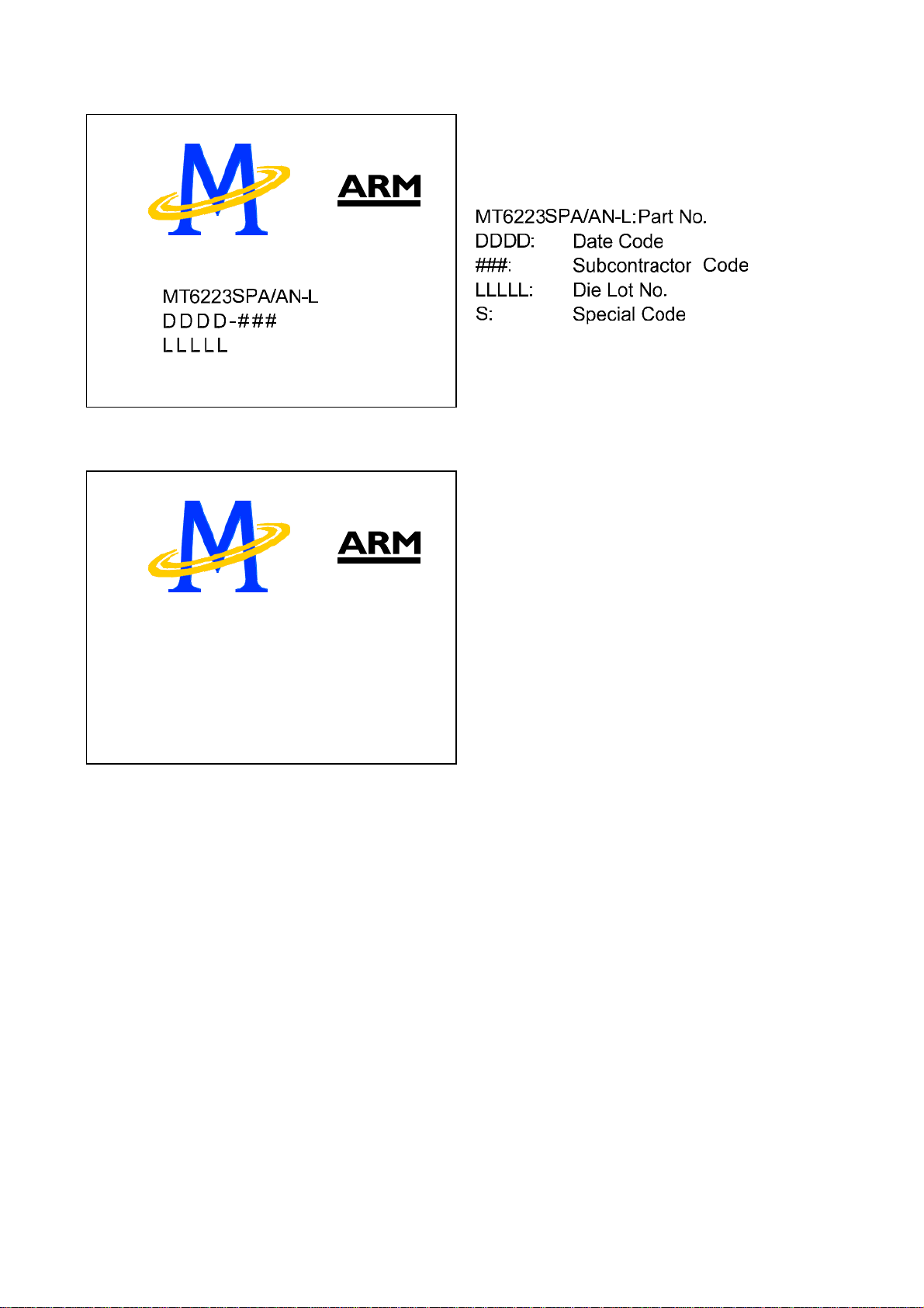
Non-security version (MT6223)
MT6223AA/AN-L
DDDD-###
LLLLL
S
MT6223AA/AN-L: Part No.
DDDD: Date Code
###: Subcontractor Code
LLLLL: Die Lot No.
S: Special Code
S
18/344 MediaTek Inc. Confidential
#
Page 19

DC Characteristics
2.2.1 Absolute Maximum Ratings
Prolonged exposure to absolute maximum ratings may reduce device reliability. Functional operation at these maximum
ratings is not implied.
Item Symbol Min Max Unit
IO power supply VDD33 -0.3 VDD33+0.3 V
I/O input voltage VDD33I -0.3 VDD33+0.3 V
Operating temperature Topr -20 80 Celsius
Storage temperature Tstg -55 125 Celsius
19/344 MediaTek Inc. Confidential
Page 20

2.3 Pin Description
Below pin description is identical for both MT6223.
BGA NAME Dir PIN DESCRIPTION Aux Func.0 Aux Func.1 Aux Func.2 Aux Func.3 PU/PD Reset
Analog Baseband Interface
F2 AU_MOUTL Audio analog output left channel
F1 AU_MOUTR Audio analog output right channel
E3 AU_FMINR FM radio analog input right channel
F3 AU_FMINL FM radio analog input left channel
G1 AU_OUT0_N Earphone 0 amplifier output (-)
G2 AU_OUT0_P Earphone 0 amplifier output (+)
G3 AU_MICBIAS_P Microphone bias supply (+)
H2 AU_MICBIAS_N Microphone bias supply (-)
H4 AU_VREF_PO Audio reference voltage (+)
H3 AU_VREF_NI Audio reference voltage (-)
J1 AU_VIN0_P Microphone 0 amplifier input (+)
J2 AU_VIN0_N Microphone 0 amplifier input (-)
K1 AU_VIN1_N Microphone 1 amplifier input (-)
K2 AU_VIN1_P Microphone 1 amplifier input (+)
L1 BDLAQP Quadrature (Q+) baseband codec
L2 BDLAQN Quadrature (Q-) baseband codec
L3 BDLAIN Quadrature (I-) baseband codec
L4 BDLAIP Quadrature (I+) baseband codec
N1 APC Automatic power control DAC output
M2 AUXADIN0 Auxiliary ADC input 0
M3 AUXADIN1 Auxiliary ADC input 1
N2 AUXADIN2 Auxiliary ADC input 2
N3 AUX_REF Reference voltage of Auxiliary ADC
R1 AFC Automatic frequency control DAC output
P2 AFC_BYP Automatic frequency control DAC bypass capacitance
RF control circuitry
R2 BPI_BUS0 O RF hard-wire control bus bit 0
T2 BPI_BUS1 O RF hard-wire control bus bit 1
R3 BPI_BUS2 O RF hard-wire control bus bit 2
U3 BPI_BUS3 O RF hard-wire control bus bit 3
T3 BPI_BUS4 O RF hard-wire control bus bit 4
P3 BPI_BUS5 O RF hard-wire control bus bit 5
R4 BPI_BUS6 IO RF hard-wire control bus bit 6 GPIO20 BPI_BUS6 XADMUX PD
T4 BPI_BUS7 IO RF hard-wire control bus bit 7 GPIO21 BPI_BUS7 BSI_RFIN clk_out0 PD
U4 BPI_BUS8 IO RF hard-wire control bus bit 8 GPIO22 BPI_BUS8 KCOL5 clk_out1 PU
U5 BPI_BUS9 IO RF hard-wire control bus bit 9 GPIO23 BPI_BUS9 BSI_CS1 clk_out2 PD
T5 BSI_CS0 O RF 3-wire control interface chip select 0
R5 BSI_DATA IO RF 3-wire control interface data output
U6 BSI_CLK O RF 3-wire control interface clock output
Digital Audio Interface (DAI)
T6 DAICLK IO DAI interface clock output
GPIO15
DAICLK EDICK PU
20/344 MediaTek Inc. Confidential
Page 21

U7 DAIPCMOUT IO DAI PCM data output
T7 DAIPCMIN IO DAI PCM data input GPIO17 DAIPCMIN PU
R6 DAIRST IO DAI reset signal input GPIO18 DAIRST PU
P6 DAISYNC IO DAI frame synchronization input GPIO19 DAISYNC EDIWS PU
PWM Interface
R7 ALERTER IO Pulse-width modulated signal for buzzer
P7 PWM IO Pulse-width modulated signal GPIO25 PWM PD
JTAG Interface
U8 JRTCK O JTAG test port returned clock output
R8 JTRST_B I JTAG test port reset input GPIO26 JTRST_B EINT4 PD
U9 JTCK I JTAG test port clock input PU
P8 JTDI I JTAG test port data input GPIO27 JTDI EINT5 PU
T9 JTMS I JTAG test port mode switch GPIO28 JTMS EINT6 PU
R9 JTDO O JTAG test port data output
Parallel LCD Interface
T10 LCD_D8 IO Parallel display interface Data 8
R10 LCD_D7 IO Parallel display interface Data 7 GPIO1 LCD_D7 PD
P10 LCD_D6 IO Parallel display interface Data 6 GPIO2 LCD_D6 PD
U10 LCD_D5 IO Parallel display interface Data 5 GPIO3 LCD_D5 PD
U11 LCD_D4 IO Parallel display interface Data 4 GPIO4 LCD_D4 PD
T11 LCD_D3 IO Parallel display interface Data 3 GPIO5 LCD_D3 PD
R11 LCD_D2 IO Parallel display interface Data 2 GPIO6 LCD_D2 PD
U12 LCD_D1 IO Parallel display interface Data 1 GPIO7 LCD_D1 PD
T12 LCD_RSTB O Parallel display interface Reset Signal GPIO8 LCD_RSTB PU
R12 LCD_WR_B O Parallel display interface Write Strobe GPIO9 LCD_WR_B PU
U13 LCD_RD_B O Parallel display interface Read Strobe GPIO10 LCD_RD_B PU
T13 LCD_D0 IO Parallel display interface Data 0 GPIO11 LCD_D0 PD
R13 LCD_A0 O Parallel display interface address output GPIO12 LCD_A0 PU
R14 LCD_CS0_B O Parallel display interface chip select 0 output GPIO13 LCD_CS0_B PU
U14 LCD_CS1_B O Parallel display interface chip select 1 output GPIO14 LCD_CS1_B EINT7 PU
External Memory Interface
U15 EADV_B O Flash, PSRAM and CellularRAM address valid, active low
T15 EWAIT O Flash, PSRAM and CellularRAM data ready PU
U16 ECLK O Flash, PSRAM and CellularRAM clock
P13 EA25 IO External memory CRE pin
T16 ED0 IO External memory data bus 0
U17 ED1 IO External memory data bus 1
T17 ED2 IO External memory data bus 2
P14 ED3 IO External memory data bus 3
R16 ED4 IO External memory data bus 4
R17 ED5 IO External memory data bus 5
P17 ED6 IO External memory data bus 6
P16 ED7 IO External memory data bus 7
P15 ED8 IO External memory data bus 8
N17 ED9 IO External memory data bus 9
N16 ED10 IO External memory data bus 10
N15 ED11 IO External memory data bus 11
M17 ED12 IO External memory data bus 12
GPIO16
GPIO24
GPIO0
DAIPCMOUT EDIDAT PD
ALERTER PD
PU
LCD_D8 PD
21/344 MediaTek Inc. Confidential
Page 22

M16 ED13 IO External memory data bus 13
M15 ED14 IO External memory data bus 14
L17 ED15 IO External memory data bus 15
L16 ERD_B O External memory read strobe, active low
L15 EWR_B O External memory write strobe, active low
L14 ECS0_B O External memory chip select 0
K17 ECS1_B O External memory chip select 1
K16 ECS2_B O External memory chip select 2
K15 ECS3_B O External memory chip select 3 MFIQ ECS3 PU
K14 ELB_B O External memory lower byte strobe
J17 EUB_B O External memory upper byte strobe
J16 EA0 O External memory address bus 0 GPIO30 EA0 EA25 PD
J15 EA1 O External memory address bus 1
J14 EA2 O External memory address bus 2
H17 EA3 O External memory address bus 3
H16 EA4 O External memory address bus 4
H15 EA5 O External memory address bus 5
G17 EA6 O External memory address bus 6
G16 EA7 O External memory address bus 7
G15 EA8 O External memory address bus 8
F17 EA9 O External memory address bus 9
F16 EA10 O External memory address bus 10
F15 EA11 O External memory address bus 11
E17 EA12 O External memory address bus 12
E16 EA13 O External memory address bus 13
E15 EA14 O External memory address bus 14
E14 EA15 O External memory address bus 15
D17 EA16 O External memory address bus 16
D16 EA17 O External memory address bus 17
D15 EA18 O External memory address bus 18
D14 EA19 O External memory address bus 19
C17 EA20 O External memory address bus 20
C16 EA21 O External memory address bus 21
C14 EA22 O External memory address bus 22
B17 EA23 O External memory address bus 23
B16 EA24 O External memory address bus 24
System Miscellaneous
J10 TESTMODE I Factory test mode enable input
T8 SYSRST_B I System reset input active low PU
T14 WATCHDOG O Watchdog reset output, active low GPIO29 WATCHDOG
A17 SRCLKENAI I External VCTCXO enable input GPIO31 SRCLKENAI PD
A16 SRCLKENA O External VCTCXO enable output active high
Keypad Interface
A15 KCOL4 I Keypad column 4
B15 KCOL3 I Keypad column 3 GPIO33 KCOL3 PU
A14 KCOL2 I Keypad column 2 GPIO34 KCOL2 PU
B14 KCOL1 I Keypad column 1 GPIO35 KCOL1 PU
A13 KCOL0 I Keypad column 0 GPIO36 KCOL0 PU
GPIO32
PD
KCOL4 PU
22/344 MediaTek Inc. Confidential
Page 23

B13 KROW4 O Keypad row 4
C13 KROW3 O Keypad row 3 GPIO38 KROW3
A12 KROW2 O Keypad row 2 GPIO39 KROW2
B12 KROW1 O Keypad row 1 GPIO40 KROW1
C12 KROW0 O Keypad row 0 GPIO41 KROW0
External Interrupt Inputs
D12 EINT0 I External interrupt 0
B11 EINT1 I External interrupt 1 EINT1 PU
C11 EINT2 I External interrupt 2 GPIO42 EINT2 MIRQ BT PU
D11 EINT3 I External interrupt 3 GPIO43 EINT3 BE PU
UART
C10 UTXD1 O UART 1 transmit data
D10 UCTS1_B I UART 1 clear to send, active low GPIO45 UCTS1_B SCL PU
C9 URTS1_B O UART 1 request to send, active low GPIO46 URTS1_B SDA PU
A9 UTXD3 IO UART 3 transmit data GPIO47 UTXD3 UCTS2_B clk_out3 PU
B9 URXD3 IO UART 3 receive data GPIO48 URXD3 URTS2_B clk_out4 PU
C8 URXD2 IO UART2 receive data GPIO49 URXD2 clk_out5 PU
C7 URXD1 I UART 1 receive data GPIO50 URXD1 PU
D8 UTXD2 IO UART2 transmit data GPIO51 UTXD2 PU
Crystal and Clock Inputs
U1 SYSCLK 13MHz or 26MHz system clock input
A11 XIN 32.768 KHz crystal input
A10 XOUT 32.768 KHz crystal output
SIM Card Interface
B5 SIMIO IO SIM Data Input / Outputs
C6 SIMRST SIM card reset output
D6 SIMCLK SIM card clock output
Charger and LED Driving Interface
D5 CHRIN Charger input
C4 GATEDRV
G10 LED_B
G9 LED_G
H8 LED_R
D4 LED
G8 VIBRATOR Vibrator driving output
LDO Outputs
A5 VSIM LDO output to SIM card
A8 VRF RF LDO output
B8 VRF_SENSE RF LDO output sensing input
A7 VCORE Digital core voltage LDO output
B7 VIO Digital I/O voltage LDO output
B6 VM External memory LDO output
C1 VA Analog LDO output
E2 VCTXO Crystal or VCTCXO LDO output
PMIC Miscellaneous
A3 VBAT_RF RF used battery voltage input
B3 VBAT Battery voltage input
B2 VBAT Battery voltage input
GPIO37
GPIO44
KROW4
EINT0 PU
UTXD1 PU
23/344 MediaTek Inc. Confidential
Page 24

A1 VBAT Battery voltage input
A2 AVBAT Battery voltage input
D7 BAT_BACKUP
C5 BATDET Battery detection input
A4 BATSENSE Battery sense input
B4 ISENSE Current sense input
C2 RESET Powr on reset
D2 RSTCAP Reset capacitor connection point
B1 VREF Reference voltage for PMIC
E4 VMSEL Memory supply voltage level select input
D3 PWRKEY Power key press input
Digital Power and Grounds
J8 PGND PMIC ground
H7 DGND PMIC ground
H11 DGND PMIC ground
H10 DGND PMIC ground
H9 DGND PMIC ground
K7 VSS33 Groud of chip digital part I/O circuitry
L8 VSS33 Groud of chip digital part I/O circuitry
K8 VSS33 Groud of chip digital part I/O circuitry
J11 VSS33 Groud of chip digital part I/O circuitry
J7 VSS33 Groud of chip digital part I/O circuitry
L9 VSS33_EMI Groud of external memory interface
K9 VSS33_EMI Groud of external memory interface
L10 VSS33_EMI Groud of external memory interface
K10 VSS33_EMI Groud of external memory interface
K11 VSS33_EMI Groud of external memory interface
N4 VDDK Supply voltage of digital core circuitry
P9 VDDK Supply voltage of digital core circuitry
D9 VDDK Supply voltage of digital core circuitry
H14 VDDK Supply voltage of digital core circuitry
D13 VDD33 Supply voltage of digital part I/O circuitry
P4 VDD33 Supply voltage of digital part I/O circuitry
P5 VDD33 Supply voltage of digital part I/O circuitry
P11 VDD33_LCD Supply voltage of display interface I/O circuitry
P12 VDD33_EMI Supply voltage of external memory interface
N14 VDD33_EMI Supply voltage of external memory interface
M14 VDD33_EMI Supply voltage of external memory interface
G14 VDD33_EMI Supply voltage of external memory interface
F14 VDD33_EMI Supply voltage of external memory interface
Analog Power and Grounds
K4 AVDD_RFE
F4 AVDD_MBUFL
J4 AVDD_GSMRFRX
M4 AVDD_PLL
E1 AVDD_AFE
G4 AVSS_MBUFL
T1 AVSS_PLL
24/344 MediaTek Inc. Confidential
Page 25

M1 AVSS_GSMRFRX
P1 AVSS_RFE
J3 AVSS_AFE
D1 AGND
A6 AGND_RF
H1 AGND_AFE
K3 AGND_RFE
B10 AVDD_RTC Supply voltage of real time clock circuitry
Table 2 Pin Descriptions (Bolded types are functions at reset)
25/344 MediaTek Inc. Confidential
Page 26

Power Description
NAME IO Supply IO GND Core Supply Core GND Remark
AU_MOUTL
AU_MOUTR
AU_FMINR
AU_FMINL
AU_OUT0_N
AU_OUT0_P
AU_MICBIAS_P
AU_MICBIAS_N
AU_VREF_PO
AU_VREF_NI
AU_VIN0_P
AU_VIN0_N
AU_VIN1_N
AU_VIN1_P
BDLAQP
BDLAQN
BDLAIN
BDLAIP
APC
AUXADIN0
AUXADIN1
AUXADIN2
AUX_REF
AFC
AFC_BYP
BPI_BUS0 VDD33 VSS33 VDDK VSSK
BPI_BUS1 VDD33 VSS33 VDDK VSSK
BPI_BUS2 VDD33 VSS33 VDDK VSSK
BPI_BUS3 VDD33 VSS33 VDDK VSSK
BPI_BUS4 VDD33 VSS33 VDDK VSSK
BPI_BUS5 VDD33 VSS33 VDDK VSSK
BPI_BUS6 VDD33 VSS33 VDDK VSSK
BPI_BUS7 VDD33 VSS33 VDDK VSSK
BPI_BUS8 VDD33 VSS33 VDDK VSSK
BPI_BUS9 VDD33 VSS33 VDDK VSSK
BSI_CS0 VDD33 VSS33 VDDK VSSK
BSI_DATA VDD33 VSS33 VDDK VSSK
BSI_CLK VDD33 VSS33 VDDK VSSK
DAICLK VDD33 VSS33 VDDK VSSK
DAIPCMOUT VDD33 VSS33 VDDK VSSK
DAIPCMIN VDD33 VSS33 VDDK VSSK
DAIRST VDD33 VSS33 VDDK VSSK
DAISYNC VDD33 VSS33 VDDK VSSK
26/344 MediaTek Inc. Confidential
Page 27

ALERTER VDD33 VSS33 VDDK VSSK
PWM VDD33 VSS33 VDDK VSSK
JRTCK VDD33 VSS33 VDDK VSSK
JTRST_B VDD33 VSS33 VDDK VSSK
JTCK VDD33 VSS33 VDDK VSSK
JTDI VDD33 VSS33 VDDK VSSK
JTMS VDD33 VSS33 VDDK VSSK
JTDO VDD33 VSS33 VDDK VSSK
LCD_D8 VDD33_LCD VSS33 VDDK VSSK
LCD_D7 VDD33_LCD VSS33 VDDK VSSK
LCD_D6 VDD33_LCD VSS33 VDDK VSSK
LCD_D5 VDD33_LCD VSS33 VDDK VSSK
LCD_D4 VDD33_LCD VSS33 VDDK VSSK
LCD_D3 VDD33_LCD VSS33 VDDK VSSK
LCD_D2 VDD33_LCD VSS33 VDDK VSSK
LCD_D1 VDD33_LCD VSS33 VDDK VSSK
LCD_RSTB VDD33_LCD VSS33 VDDK VSSK
LCD_WR_B VDD33_LCD VSS33 VDDK VSSK
LCD_RD_B VDD33_LCD VSS33 VDDK VSSK
LCD_D0 VDD33_LCD VSS33 VDDK VSSK
LCD_A0 VDD33_LCD VSS33 VDDK VSSK
LCD_CS0_B VDD33_LCD VSS33 VDDK VSSK
LCD_CS1_B VDD33_LCD VSS33 VDDK VSSK
EADV_B VDD33_EMI VSS33 VDDK VSSK
EWAIT VDD33_EMI VSS33 VDDK VSSK
ECLK VDD33_EMI VSS33 VDDK VSSK
EA25 VDD33_EMI VSS33 VDDK VSSK
ED0 VDD33_EMI VSS33 VDDK VSSK
ED1 VDD33_EMI VSS33 VDDK VSSK
ED2 VDD33_EMI VSS33 VDDK VSSK
ED3 VDD33_EMI VSS33 VDDK VSSK
ED4 VDD33_EMI VSS33 VDDK VSSK
ED5 VDD33_EMI VSS33 VDDK VSSK
ED6 VDD33_EMI VSS33 VDDK VSSK
ED7 VDD33_EMI VSS33 VDDK VSSK
ED8 VDD33_EMI VSS33 VDDK VSSK
ED9 VDD33_EMI VSS33 VDDK VSSK
ED10 VDD33_EMI VSS33 VDDK VSSK
ED11 VDD33_EMI VSS33 VDDK VSSK
ED12 VDD33_EMI VSS33 VDDK VSSK
ED13 VDD33_EMI VSS33 VDDK VSSK
ED14 VDD33_EMI VSS33 VDDK VSSK
ED15 VDD33_EMI VSS33 VDDK VSSK
ERD_B VDD33_EMI VSS33 VDDK VSSK
27/344 MediaTek Inc. Confidential
Page 28

EWR_B VDD33_EMI VSS33 VDDK VSSK
ECS0_B VDD33_EMI VSS33 VDDK VSSK
ECS1_B VDD33_EMI VSS33 VDDK VSSK
ECS2_B VDD33_EMI VSS33 VDDK VSSK
ECS3_B VDD33_EMI VSS33 VDDK VSSK
ELB_B VDD33_EMI VSS33 VDDK VSSK
EUB_B VDD33_EMI VSS33 VDDK VSSK
EA0 VDD33_EMI VSS33 VDDK VSSK
EA1 VDD33_EMI VSS33 VDDK VSSK
EA2 VDD33_EMI VSS33 VDDK VSSK
EA3 VDD33_EMI VSS33 VDDK VSSK
EA4 VDD33_EMI VSS33 VDDK VSSK
EA5 VDD33_EMI VSS33 VDDK VSSK
EA6 VDD33_EMI VSS33 VDDK VSSK
EA7 VDD33_EMI VSS33 VDDK VSSK
EA8 VDD33_EMI VSS33 VDDK VSSK
EA9 VDD33_EMI VSS33 VDDK VSSK
EA10 VDD33_EMI VSS33 VDDK VSSK
EA11 VDD33_EMI VSS33 VDDK VSSK
EA12 VDD33_EMI VSS33 VDDK VSSK
EA13 VDD33_EMI VSS33 VDDK VSSK
EA14 VDD33_EMI VSS33 VDDK VSSK
EA15 VDD33_EMI VSS33 VDDK VSSK
EA16 VDD33_EMI VSS33 VDDK VSSK
EA17 VDD33_EMI VSS33 VDDK VSSK
EA18 VDD33_EMI VSS33 VDDK VSSK
EA19 VDD33_EMI VSS33 VDDK VSSK
EA20 VDD33_EMI VSS33 VDDK VSSK
EA21 VDD33_EMI VSS33 VDDK VSSK
EA22 VDD33_EMI VSS33 VDDK VSSK
EA23 VDD33_EMI VSS33 VDDK VSSK
EA24 VDD33_EMI VSS33 VDDK VSSK
TESTMODE VDD33 VSS33 VDDK VSSK
SYSRST_B VDD33 VSS33 VDDK VSSK
WATCHDOG VDD33_EMI VSS33 VDDK VSSK
SRCLKENAI VDD33 VSS33 VDDK VSSK
SRCLKENA VDD33 VSS33 VDDK VSSK
KCOL4 VDD33 VSS33 VDDK VSSK
KCOL3 VDD33 VSS33 VDDK VSSK
KCOL2 VDD33 VSS33 VDDK VSSK
KCOL1 VDD33 VSS33 VDDK VSSK
KCOL0 VDD33 VSS33 VDDK VSSK
KROW4 VDD33 VSS33 VDDK VSSK
KROW3 VDD33 VSS33 VDDK VSSK
KROW2 VDD33 VSS33 VDDK VSSK
KROW1 VDD33 VSS33 VDDK VSSK
28/344 MediaTek Inc. Confidential
Page 29

KROW0 VDD33 VSS33 VDDK VSSK
EINT0 VDD33 VSS33 VDDK VSSK
EINT1 VDD33 VSS33 VDDK VSSK
EINT2 VDD33 VSS33 VDDK VSSK
EINT3 VDD33 VSS33 VDDK VSSK
UTXD1 VDD33 VSS33 VDDK VSSK
UCTS1_B VDD33 VSS33 VDDK VSSK
URTS1_B VDD33 VSS33 VDDK VSSK
UTXD3 VDD33 VSS33 VDDK VSSK
URXD3 VDD33 VSS33 VDDK VSSK
URXD2 VDD33 VSS33 VDDK VSSK
URXD1 VDD33 VSS33 VDDK VSSK
UTXD2 VDD33 VSS33 VDDK VSSK
SYSCLK AVDD_PLL AVSS_PLL AVDD_PLL AVSS_PLL
XIN AVDD_RTC AVSS_RTC AVDD_RTC AVSS_RTC
XOUT AVDD_RTC AVSS_RTC AVDD_RTC AVSS_RTC
SIMIO VSIM
SIMRST VSIM
SIMCLK VSIM
CHRIN
GATEDRV
LED_B
LED_G
LED_R
LED
VIBRATOR
VSIM 3.3/1.8V
VRF 2.8V
VRF_SENSE
VCORE 1.8/1.5V
VIO 2.8V
VM 2.8/1.8V
VA 2.8V
VCTXO 2.8V
VBAT_RF
VBAT
VBAT
VBAT
AVBAT
BAT_BACKUP
BATDET
29/344 MediaTek Inc. Confidential
Page 30

BATSENSE
ISENSE
RESET
RSTCAP
VREF
VMSEL
PWRKEY
PGND
DGND
DGND
DGND
DGND
VSS33
VSS33
VSS33
VSS33
VSS33
VSS33_EMI
VSS33_EMI
VSS33_EMI
VSS33_EMI
VSS33_EMI
VDDK TYP 1.8V
VDDK TYP 1.8V
VDDK TYP 1.8V
VDDK TYP 1.8V
VDD33 TYP 2.8V
VDD33 TYP 2.8V
VDD33 TYP 2.8V
VDD33_LCD 2.8V/1.8V
VDD33_EMI 2.8V/1.8V
VDD33_EMI 2.8V/1.8V
VDD33_EMI 2.8V/1.8V
VDD33_EMI 2.8V/1.8V
VDD33_EMI 2.8V/1.8V
AVDD_RFE
AVDD_MBUFL
AVDD_GSMRFRX
AVDD_PLL
AVDD_AFE
AVSS_MBUFL
AVSS_PLL
AVSS_GSMRFRX
AVSS_RFE
AVSS_AFE
AGND
30/344 MediaTek Inc. Confidential
Page 31

AGND_RF
AGND_AFE
AGND_RFE
AVDD_RTC
Table 3 Power Descriptions
2.4 Digital Pin Electrical Characteristics
Based on I/O power supply (VDD33) = 3.3 V
Vil (max) = 0.8 V
Vih (min) = 2.0 V
PU/PD
Resistor(K ohm)
Voh at max.
Ball GPIO Driving(mA) Pull Vol at max. Iol
Ioh
BPI
BPI_BUS0 min 2, max 8 0.4 2.4
BPI_BUS1 min 2, max 8 0.4 2.4
BPI_BUS2 min 2, max 8 0.4 2.4
BPI_BUS3 min 2, max 8 0.4 2.4
BPI_BUS4 2 0.4 2.4
BPI_BUS5 2 0.4 2.4
BPI_BUS6 GPIO20 2 PD 0.4 2.4 5.2
BPI_BUS7 GPIO21 2 PD 0.4 2.4 40, 75, 190 5.2
BPI_BUS8 GPIO22 2 PU 0.4 2.4 5.2
BPI_BUS9 GPIO23 2 PD 0.4 2.4 5.2
BSI
BSI_CS0 2 0.4 2.4
BSI_DATA 2 0.4 2.4
BSI_CLK 2 0.4 2.4
DAI
DAICLK GPIO15 6 PU 0.4 2.4 40, 75, 190 5.2
DAIPCMOUT GPIO16 6 PD 0.4 2.4 40, 75, 190 5.2
DAIPCMIN GPIO17 6 PU 0.4 2.4 40, 75, 190 5.2
DAIRST GPIO18 6 PU 0.4 2.4 40, 75, 190 5.2
DAISYNC GPIO19 6 PU 0.4 2.4 40, 75, 190 5.2
ALERTER GPIO24 4 PD 0.4 2.4 40, 75, 190 5.2
PWM GPIO25 4 PD 0.4 2.4 40, 75, 190 5.2
JTAG
JRTCK 6 PU 0.4 2.4 40, 75, 190 5.2
JTRST_B GPIO26 2 PD 0.4 2.4 40, 75, 190 5.2
JTCK input only PU 40, 75, 190 5.2
(min, typical,
max)
Cin(pF)
31/344 MediaTek Inc. Confidential
Page 32

JTDI GPIO27 2 PU 0.4 2.4 40, 75, 190 5.2
JTMS GPIO28 2 PU 0.4 2.4 40, 75, 190 5.2
JTDO 6 PU 0.4 2.4 40, 75, 190 5.2
SYSRST_B input only PU 40, 75, 190 5.2
LCD
LCD_D8 GPIO0 max 16, min 2 PD 0.4 2.4 40, 75, 190 5.2
LCD_D7 GPIO1 max 16, min 2 PD 0.4 2.4 40, 75, 190 5.2
LCD_D6 GPIO2 max 16, min 2 PD 0.4 2.4 40, 75, 190 5.2
LCD_D5 GPIO3 max 16, min 2 PD 0.4 2.4 40, 75, 190 5.2
LCD_D4 GPIO4 max 16, min 2 PD 0.4 2.4 40, 75, 190 5.2
LCD_D3 GPIO5 max 16, min 2 PD 0.4 2.4 40, 75, 190 5.2
LCD_D2 GPIO6 max 16, min 2 PD 0.4 2.4 40, 75, 190 5.2
LCD_D1 GPIO7 max 16, min 2 PD 0.4 2.4 40, 75, 190 5.2
LCD_RSTB GPIO8 max 16, min 2 PU 0.4 2.4 40, 75, 190 5.2
LCD_WR_B GPIO9 max 16, min 2 PU 0.4 2.4 40, 75, 190 5.2
LCD_RD_B GPIO10 max 16, min 2 PU 0.4 2.4 40, 75, 190 5.2
LCD_D0 GPIO11 max 16, min 2 PD 0.4 2.4 40, 75, 190 5.2
LCD_A0 GPIO12 max 16, min 2 PU 0.4 2.4 40, 75, 190 5.2
LCD_CS0_B GPIO13 max 16, min 2 PU 0.4 2.4 40, 75, 190 5.2
LCD_CS1_B GPIO14 max 16, min 2 PU 0.4 2.4 40, 75, 190 5.2
WATCHDOG GPIO29 4 0.4 2.4 5.2
EMI
EADV_B max 16, min 2 0.4 2.4
EWAIT max 16, min 2 PU 0.4 2.4 40, 75, 190
ECLK max 16, min 2 0.4 2.4
ECRE max 16, min 2 0.4 2.4
ED0 max 16, min 2 0.4 2.4 5.2
ED1 max 16, min 2 0.4 2.4 5.2
ED2 max 16, min 2 0.4 2.4 5.2
ED3 max 16, min 2 0.4 2.4 5.2
ED4 max 16, min 2 0.4 2.4 5.2
ED5 max 16, min 2 0.4 2.4 5.2
ED6 max 16, min 2 0.4 2.4 5.2
ED7 max 16, min 2 0.4 2.4 5.2
ED8 max 16, min 2 0.4 2.4 5.2
ED9 max 16, min 2 0.4 2.4 5.2
ED10 max 16, min 2 0.4 2.4 5.2
ED11 max 16, min 2 0.4 2.4 5.2
ED12 max 16, min 2 0.4 2.4 5.2
ED13 max 16, min 2 0.4 2.4 5.2
ED14 max 16, min 2 0.4 2.4 5.2
ED15 max 16, min 2 0.4 2.4 5.2
ERD_B max 16, min 2 0.4 2.4
32/344 MediaTek Inc. Confidential
Page 33

EWR_B max 16, min 2 0.4 2.4
ECS0_B max 16, min 2 0.4 2.4
ECS1_B max 16, min 2 0.4 2.4
ECS2_B max 16, min 2 0.4 2.4
ECS3_B max 16, min 2 PU 0.4 2.4 40, 75, 190
ELB_B max 16, min 2 0.4 2.4
EUB_B max 16, min 2 0.4 2.4
EA0 GPIO30 max 16, min 2 PD 0.4 2.4 40, 75, 190
EA1 max 16, min 2 0.4 2.4
EA2 max 16, min 2 0.4 2.4
EA3 max 16, min 2 0.4 2.4
EA4 max 16, min 2 0.4 2.4
EA5 max 16, min 2 0.4 2.4
EA6 max 16, min 2 0.4 2.4
EA7 max 16, min 2 0.4 2.4
EA8 max 16, min 2 0.4 2.4
EA9 max 16, min 2 0.4 2.4
EA10 max 16, min 2 0.4 2.4
EA11 max 16, min 2 0.4 2.4
EA12 max 16, min 2 0.4 2.4
EA13 max 16, min 2 0.4 2.4
EA14 max 16, min 2 0.4 2.4
EA15 max 16, min 2 0.4 2.4
EA16 max 16, min 2 0.4 2.4
EA17 max 16, min 2 0.4 2.4
EA18 max 16, min 2 0.4 2.4
EA19 max 16, min 2 0.4 2.4
EA20 max 16, min 2 0.4 2.4
EA21 max 16, min 2 0.4 2.4
EA22 max 16, min 2 0.4 2.4
EA23 max 16, min 2 0.4 2.4
EA24 max 16, min 2 0.4 2.4
SRCLKENAI GPIO31 2 PD 0.4 2.4 40, 75, 190 5.2
SRCLKENA 2 0.4 2.4
Key pad
KCOL4 GPIO32 6 PU 0.4 2.4 40, 75, 190 5.2
KCOL3 GPIO33 6 PU 0.4 2.4 40, 75, 190 5.2
KCOL2 GPIO34 6 PU 0.4 2.4 40, 75, 190 5.2
KCOL1 GPIO35 6 PU 0.4 2.4 40, 75, 190 5.2
KCOL0 GPIO36 6 PU 0.4 2.4 40, 75, 190 5.2
KROW4 GPIO37 6 0.4 2.4 5.2
KROW3 GPIO38 6 0.4 2.4 5.2
KROW2 GPIO39 6 0.4 2.4 5.2
33/344 MediaTek Inc. Confidential
Page 34

KROW1 GPIO40 2 0.4 2.4 5.2
KROW0 GPIO41 2 0.4 2.4 5.2
EINT
EINT0 input only PU 40, 75, 190 5.2
EINT1 input only PU 40, 75, 190 5.2
EINT2 GPIO42 2 PU 0.4 2.4 40, 75, 190 5.2
EINT3 GPIO43 2 PU 0.4 2.4 40, 75, 190 5.2
UART
UTXD1 GPIO44 2 PU 0.4 2.4 40, 75, 190 5.2
UCTS1_B GPIO45 2 PU 0.4 2.4 40, 75, 190 5.2
URTS1_B GPIO46 2 PU 0.4 2.4 40, 75, 190 5.2
UTXD3 GPIO47 2 PU 0.4 2.4 40, 75, 190 5.2
URXD3 GPIO48 2 PU 0.4 2.4 40, 75, 190 5.2
URXD2 GPIO49 2 PU 0.4 2.4 40, 75, 190 5.2
URXD1 GPIO50 2 PU 0.4 2.4 40, 75, 190 5.2
UTXD2 GPIO51 2 PU 0.4 2.4 40, 75, 190 5.2
34/344 MediaTek Inc. Confidential
Page 35

3 Micro-Controller Unit Subsystem
Figure 5 illustrates the block diagram of the Micro-Controller Unit Subsystem in MT6223. The subsystem utilizes a main
32-bit ARM7EJ-S RISC processor, which plays the role of the main bus master controlling the whole subsystem. The
processor communicates with all the other on-chip modules via the two-level system buses: AHB Bus and APB Bus. All bus
transactions originate from bus masters, while slaves can only respond to requests from bus masters. Before data transfer can
be established, bus master must ask for bus ownership. This is accomplished by request-grant handshaking protocol between
masters and arbiters.
The bus comprises of two-level system buses: Advanced High-Performance Bus (AHB) and Advanced Peripheral Bus (APB).
All bus transactions originate from bus masters, while slaves can only respond to requests from bus masters. Before data
transfer can be established, the bus master must ask for bus ownership, accomplished by request-grant handshaking protocol
between masters and arbiters.
Two levels of bus hierarchy are designed to provide optimum usage for different performance requirements. Specifically,
AHB Bus, the main system bus, is tailored toward high-speed requirements and provides 32-bit data path with multiplex
scheme for bus interconnections. The APB Bus, on the other hand, is designed to reduce interface complexity for lower
data transfer rate, and so it is isolated from high bandwidth AHB Bus by APB Bridge. APB Bus supports 16-bit addressing
and both 16-bit and 32-bit data paths. APB Bus is also optimized for minimal power consumption by turning off the clock
when there is no APB bus activity.
During operation, if the target slave is located on AHB Bus, the transaction is conducted directly on AHB Bus. However, if
the target slave is a peripheral and is attached to the APB bus, then the transaction is conducted between AHB and APB bus
through the use of APB Bridge.
The MT6223 MCU subsystem supports only memory addressing method. Therefore all components are mapped onto the
MCU 32-bit address space. A Memory Management Unit is employed to allow for a central decode scheme. The MMU
generates appropriate selection signals for each memory-addressed module on the AHB Bus.
In order to off-load the processor core, a DMA Controller is designated to act as a master and share the bus resources on AHB
Bus to do fast data movement between modules. This controller comprises thirteen DMA channels.
The Interrupt Controller provides a software interface to manipulate interrupt events. It can handle up to 32 interrupt sources
asserted at the same time. In general, it generates 2 levels of interrupt requests, FIQ and IRQ, to the processor.
A 40K Byte SRAM is provided as system memory for high-speed data access. For factory programming purposes, a Boot
ROM module is also integrated. These two modules use the same Internal Memory Controller to connect to AHB Bus.
External Memory Interface supports both 8-bit and 16-bit devices. Since AHB Bus is 32-bit wide, all the data transfer will be
converted into several 8-bit or 16-bit cycles depending on the data width of target device. Note that, this interface is specific
to both synchronous and asynchronous components, like Flash, SRAM and parallel LCD. This interface supports also page
and burst mode type of Flash.
35/344 MediaTek Inc. Confidential
Page 36

System ROM
ARM7EJ-S
DMA
Controller
Peripheral
Ext
Bus
External
Memory
Interface
System RAM
Internal Memory
Controller
MCU-DSP
Interface
Arbiter
AHB Bus
Figure 5 Block Diagram of the Micro-Controller Unit Subsystem in MT6223
3.1 Processor Core
Interrupt
Controller
APB
Bridge
APB Bus
Peripheral
3.1.1 General Description
The Micro-Controller Unit Subsystem in MT6223 is built up with a 32-bit RISC core, ARM7EJ-S that is based on Von
Neumann architecture with a single 32-bit data bus carrying both instructions and data. The memory interface of ARM7EJ-S
is totally compliant to AMBA based bus system. Basically, it can be connected to AHB Bus directly.
3.2 Memory Management
3.2.1 General Description
The processor core of MT6223, ARM7EJ-S, supports only memory addressing method for instruction fetch and data access.
It manages a 32-bit address space that has addressing capability up to 4GB. System RAM, System ROM, Registers, MCU
Peripherals and external components are all mapped onto such 32-bit address space, as depicted in Figure 6.
36/344 MediaTek Inc. Confidential
Page 37

MCU 32-bit
Addressing
Space
9FFF_FFFh
|
9000_0000h
8FFF_FFFFh
|
8000_0000h
7FFF_FFFFh
|
7000_0000h
6FFF_FFFFh
|
5000_0000h
4FFF_FFFFh
|
4000_0000h
Reserved
9800_0000h
9000_0000h LCD
APB Peripherals
7800_0000h
7000_0000h Reserved
MCU-DSP Interface
Reserved
Virtual FIFO
Internal Memory
3FFF_FFFFh
|
0000_0000h
External Memroy
EA[25:0]
Addressing
Space
Figure 6 The Memory Layout of MT6223
The address space is organized as basis of blocks with size of 256M Bytes for each. Memory blocks MB0-MB9 are
determined and currently dedicated to specific functions, as shown in Ta ble 4 , while the others are reserved for future usage.
Essentially, the block number is uniquely selected by address line A31-A28 of internal system bus.
Memory
Block
Block Address
Address Range Description
A31-A28
00000000h-07FFFFFFh Boot Code, EXT SRAM or EXT Flash/MISC
MB0 0h
08000000h-0FFFFFFFh EXT SRAM or EXT Flash/MISC
10000000h-17FFFFFFh EXT SRAM or EXT Flash/MISC
MB1 1h
18000000h-1FFFFFFFh EXT SRAM or EXT Flash/MISC
20000000h-27FFFFFFh Reserved
MB2 2h
28000000h-2FFFFFFFh Reserved
MB3 3h 30000000h-37FFFFFFh Reserved
37/344 MediaTek Inc. Confidential
Page 38

38000000h-3FFFFFFFh Reserved
40000000h-47FFFFFFh System RAM
MB4 4h
48000000h-4FFFFFFFh System ROM
MB5 5h 50000000h-5FFFFFFFh
MCU-DSP Interface
MB6 6h 60000000h-6FFFFFFFh
70000000h-77FFFFFFh Reserved
MB7 7h
78000000h-7FFFFFFFh Virtual FIFO
MB8 8h 80000000h-8FFFFFFFh APB Slaves
90000000h-97FFFFFFh LCD
MB9 9h
98000000h-9FFFFFFFh Reserved
Table 4 Definitions of Memory Blocks in MT6223
3.2.1.1 External Access
To have external access, the MT6223 outputs 26 bits (A25-A0) of address lines along with 4 selection signals that correspond
to associated memory blocks. That is, MT6223 can support at most 4 MCU addressable external components. The data width
of internal system bus is fixed as 32-bit wide, while the data width of the external components is fixed as 16 bit.
Since devices are usually available with variety operating grades, adaptive configurations for different applications are
needed. MT6223 provides software programmable registers to configure to adapt operating conditions in terms of different
wait-states.
3.2.1.2 Memory Re-mapping Mechanism
To permit system being configured with more flexible, a memory re-mapping mechanism is provided. It allows software
program to swap BANK0 (ECS0#) and BANK1 (ECS1#) dynamically. Whenever the bit value of RM0 in register
EMI_REMAP is changed, these two banks will be swapped accordingly. Besides, it also permits system being boot in
different sequence as detailed in
3.2.1.3 Boot Sequence
Since the ARM7EJ-S core always starts to fetch instructions from the lowest memory address at 00000000h after system has
been reset, the system is designed to have a dynamic mapping architecture capable of associating Boot Code, external Flash
or external SRAM with the memory block 0000_0000h – 07ff_ffffh.
By default, the Boot Code is mapped onto 0000_0000h – 07ff_ffffh after a system reset. In this special boot mode, External
Memory Controller does not access external memory; instead, the EMI Controller send predefined Boot Code back to the
ARM7EJS-S core, which instructs the processor to execute the program in System ROM. This configuration can be
changed by programming bit value of RM1 in register EMI_REMAP directly.
MT6223 system provides one boot up scheme:
3.2.1.3 Boot Sequence.
z Start up system of running codes from Boot Code for factory programming.
3.2.1.3.1 Boot Code
The Boot Code is placed together with Memory Re-Mapping Mechanism in External Memory Controller, and comprises of
38/344 MediaTek Inc. Confidential
Page 39

just two words of instructions as shown below. A jump instruction leads the processor to run the code starting at address
48000000h where the System ROM is placed.
ADDRESS BINARY CODE ASSEMBLY
00000000h E51FF004h LDR PC, 0x4
00000004h 48000000h (DATA)
3.2.1.3.2 Factory Programming
The configuration for factory programming is shown in Figure 7. Usually the Factory Programming Host connects with
MT6223 by way of UART interface. To have it works properly, the system should boot up from Boot Code. The down load
speed can be up to 921K bps while MCU is running at 26MHz.
After system being reset, the Boot Code will guide the processor to run the Factory Programming software placed in System
ROM. Then, MT6223 will start and continue to poll the UART1 port until valid information is detected. The first information
received on the UART1 will be used to configure the chip for factory programming. The Flash down loader program is then
transferred into System RAM or external SRAM.
Further information will be detailed in MT6223 Software Programming Specification.
UART
BaseBand Processor
External
Memory
Interface
FLASH
Factory
Programming
Host
Figure 7 System configuration required for factory programming
3.2.1.4 Little Endian Mode
The MT6223 system always treats 32-bit words of memory in Little Endian format. In Little Endian mode, the lowest
numbered byte in a word is stored in the least significant byte, and the highest numbered byte in the most significant position.
Byte 0 of the memory system is therefore connected to data lines 7 through 0.
3.3 Bus System
3.3.1 General Description
Two levels of bus hierarchy are employed in constructing the Micro-Controller Unit Subsystem of MT6223. As depicted in
Figure 5, AHB Bus and APB Bus serve for system backbone and peripheral buses, while an APB bridge connects these two
buses. Both AHB and APB Buses operate at the same clock rate as processor core.
The APB Bridge is the only bus master resided on the APB bus. All APB slaves are mapped onto memory block MB8 in
MCU 32-bit addressing space. A central address decoder is implemented inside the bridge to generate those select signals for
individual peripheral. In addition, since the base address of each APB slave has been associated with select signals, the
address bus on APB will contain only the value of offset address.
39/344 MediaTek Inc. Confidential
Page 40

The maximum address space that can be allocated to a single APB slave is 64KB, i.e. 16-bit address lines. The width of data
bus is mainly constrained to 16-bit to minimize the design complexity and power consumption while some of them uses
32-bit data bus to accommodate more bandwidth. In the case where an APB slave needs large amount of transfers, the device
driver can also request a DMA resource or channel to conduct a burst of data transfer. The base address and data width of
each peripheral are listed in Table 5.
Base Address Description Data Width Software Base ID
Configuration Registers
8000_0000h
16 CONFG Base
(Clock, Power Down, Version and Reset)
8001_0000h External Memory Interface 32 EMI Base
8002_0000h Interrupt Controller 32 CIRQ Base
8003_0000h DMA Controller 32 DMA Base
8004_0000h Reset Generation Unit 16 RGU Base
8005_0000h Reserved
8006_0000h GPRS Cipher Unit 32 GCU Base
8007_0000h I2C 16 I2C Base
8008_0000h Reserved
8009_0000h Software Debug 32 SWDBG base
8010_0000h General Purpose Timer 16 GPT Base
8011_0000h Keypad Scanner 16 KP Base
8012_0000h General Purpose Inputs/Outputs 16 GPIO Base
8013_0000h UART 1 16 UART1 Base
8014_0000h SIM Interface 16 SIM Base
8015_0000h Pulse-Width Modulation Outputs 16 PWM Base
8016_0000h Alerter Interface 16 ALTER Base
8017_0000h Security Engine for JTAG protection 32 SEJ Base
8018_0000h UART 2 16 UART2 Base
8019_0000h Reserved
801a_0000h Reserved
801b_0000h UART 3 16 UART3 Base
801c_0000h Reserved
8020_0000h TDMA Timer 32 TDMA Base
40/344 MediaTek Inc. Confidential
Page 41

8021_0000h Real Time Clock 16 RTC Base
8022_0000h Base-Band Serial Interface 32 BSI Base
8023_0000h Base-Band Parallel Interface 16 BPI Base
8024_0000h Automatic Frequency Control Unit 16 AFC Base
8025_0000h Automatic Power Control Unit 32 APC Base
8026_0000h Frame Check Sequence 16 FCS Base
8027_0000h Auxiliary ADC Unit 16 AUXADC Base
8028_0000h Divider/Modulus Coprocessor 32 DIVIDER Base
8029_0000h CSD Format Conversion Coprocessor 32 CSD_ACC Base
802a_0000h Reserved
8030_0000h MCU-DSP Shared Register 1 16 SHARE1 Base
8031_0000h DSP Patch Unit 1 16 PATCH1 Base
8032_0000h MCU-DSP Shared Register 2 16 SHARE2 Base
8033_0000h DSP Patch Unit 2 16 PATCH2 Base
8040_0000h Audio Front End 16 AFE Base
8041_0000h Base-Band Front End 16 BFE Base
8050_0000h Analog Chip Interface Controller 16 MIXED Base
Table 5 Register Base Addresses for MCU Peripherals
REGISTER ADDRESS REGISTER NAME SYNONYM
CONFG + 0000h Hardware Version Register HW_VER
CONFG + 0004h Software Version Register SW_VER
CONFG + 0008h Hardware Code Register HW_CODE
CONFG + 0404h APB Bus Control Register APB_CON
CONFG + 0500h AHB Bus Control Register AHB_CON
Table 6 APB Bridge Register Map
3.3.2 Register Definitions
CONFG+0000h Hardware Version Register HW_VERSION
Bit 15 14 13 12 11 10 9 8 7 6 5 4 3 2 1 0
41/344 MediaTek Inc. Confidential
Page 42

Name EXTP MAJREV MINREV
Type RO RO RO RO
Reset 8 A 0 0
This register is used by software to determine the hardware version of the chip. The register contains a new value whenever
each metal fix or major step is performed. All values are incremented by a step of 1.
MINREV Minor Revision of the chip
MAJREV Major Revision of the chip
EXTP This field shows the existence of Hardware Code Register that presents the Hardware ID while the value is other
than zero.
CONFG+0004h Software Version Register SW_VERSION
Bit 15 14 13 12 11 10 9 8 7 6 5 4 3 2 1 0
Name EXTP MAJREV MINREV
Type RO RO RO RO
Reset 8 A 0 0
This register is used by software to determine the software version used with this chip. All values are incremented by a step
of 1.
MINREV Minor Revision of the software
MAJREV Major Revision of the software
EXTP This field shows the existence of Hardware Code Register that presents the Hardware ID when the value is other
than zero.
CONFG+0008h Hardware Code Register HW_CODE
Bit 15 14 13 12 11 10 9 8 7 6 5 4 3 2 1 0
Name CODE3 CODE2 CODE1 CODE0
Type RO RO RO RO
Reset 6 2 2 3
This register presents the Hardware ID.
CODE This version of chip is coded as 6223h.
CONFG+0404h APB Bus Control Register APB_CON
Bit 15 14 13 12 11 10 9 8 7 6 5 4 3 2 1 0
Name APBW6 APBW4 APBW3 APBW2 APBW1 APBW0 APBR6 APBR4 APBR3 APBR2 APBR1 APBR0
Type R/W R/W R/W R/W R/W R/W R/W R/W R/W R/W R/W R/W
Reset 0 0 0 0 0 0 1 1 1 1 1 1
42/344 MediaTek Inc. Confidential
Page 43

This register is used to control the timing of Read Cycle and Write Cycle on APB Bus. Note that APB Bridge 5 is different
from other bridges. The access time is varied, and access is not completed until acknowledge signal from APB slave is
asserted.
APBR0-APBR6 Read Access Time on APB Bus
0 1-Cycle Access
1 2-Cycle Access
APBW0-APBW6 Write Access Time on APB Bus
0 1-Cycle Access
1 2-Cycle Access
CONFG+0500h AHB Bus Control Register AHB_CON
Bit 15 14 13 12 11 10 9 8 7 6 5 4 3 2 1 0
Name EMI
Type R/W
Reset 0
EMI Control the AHB-EMI interface
0 latch mode. In order to meet bus timing constraints, Additional stage of registers are inserted between AHB and
EMI. While running at 52MHz, AHB-EMI interface must be set as latch mode..
1 direct couple mode. AHB and EMI are directly coupled. While running at 26MHz, AHB-EMI interface must be
set as direct couple mode for better bus efficiency.
3.4 Direct Memory Access
3.4.1 General Description
A generic DMA Controller is placed on Layer 2 AHB Bus to support fast data transfers and to off-load the processor. With
this controller, specific devices on AHB or APB buses can benefit greatly from quick completion of data movement from or
to memory modules such as Internal System RAM or External SRAM. Such Generic DMA Controller can also be used to
connect any two devices other than memory module as long as they can be addressed in memory space.
Figure 8 Variety Data Paths of DMA Transfers
43/344 MediaTek Inc. Confidential
Page 44

Up to fourteen channels of simultaneous data transfers are supported. Each channel has a similar set of registers to be
configured to different scheme as desired. If more than fourteen devices are requesting the DMA resources at the same time,
software based arbitration should be employed. Once the service candidate is decided, the responsible device driver should
configure the Generic DMA Controller properly in order to conduct DMA transfers. Both Interrupt and Polling based
schemes in handling the completion event are supported. The block diagram of such generic DMA Controller is illustrated
in the following figure.
Figure 9 Block Diagram of Direct memory Access Module
3.4.1.1 Full-Size & Half-Size DMA Chann els
There are three types of DMA channels in the DMA controller. The first one is called a full-size DMA channel, the second
one is called a half-size DMA channel, and the last is Virtual FIFO DMA. Channels 1 is full-size DMA channels; channels
4 through 8 are half-size ones; and channels 11 through 14 are Virtual FIFO DMAs. The difference between the first two
types of DMA channels is that both source and destination address are programmable in full-size DMA channels, but only the
address of one side can be programmed in half-size DMA channel. In half-size channels, only either the source or
destination address can be programmed, while the addresses of the other side is preset. Which preset address is used
depends on the setting of MAS in DMA Channel Control Register. Refer to the Register Definition section for more detail.
3.4.1.2 Ring Buffer & Double Buffer Memory Data Movement
DMA channels 1 and 4 through 6 support ring-buffer and double-buffer memory data movement. This can be achieved by
programming DMA_WPPT and DMA_WPTO, as well as setting WPEN in DMA_CON register to enable. The following
figure shows how the function works. Once the transfer counter reaches the value of WPPT, the next address jumps to the
WPTO address after completing the WPPT data transfer. Note that only one side can be configured as ring-buffer or
double-buffer memory, and this is controlled by WPSD in DMA_CON register.
44/344 MediaTek Inc. Confidential
Page 45

Figure 10 Ring Buffer and Double Buffer Memory Data Movement
3.4.1.3 Unaligned Word Access
The address of word access on AHB bus must be aligned to word boundary, or the 2 LSB is truncated to 00b. If
programmers do not notice this, it may cause an incorrect data fetch. In the case where data is to be moved from unaligned
addresses to aligned addresses, the word is usually first split into four bytes and then moved byte by byte. This results in
four read and four write transfers on the bus.
To improve bus efficiency, unaligned-word access is provided in DMA4~8. While this function is enabled, DMAs move
data from unaligned address to aligned address by executing four continuous byte-read access and one word-write access,
reducing the number of transfers on the bus by three.
Figure 11 Unaligned Word Accesses
3.4.1.4 Virtual FIFO DMA
Virtual FIFO DMA is used to ease UART control. The difference between the Virtual FIFO DMAs and the ordinary DMAs
is that Virtual FIFO DMA contains additional FIFO controller. The read and write pointers are kept in the Virtual FIFO
DMA. During a read from the FIFO, the read pointer points to the address of the next data. During a write to the FIFO,
the write pointer moves to the next address. If the FIFO is empty, a FIFO read is not allowed. Similarly, data is not written
into the FIFO if the FIFO is full. Due to UART flow control requirements, an alert length is programmed. Once the FIFO
45/344 MediaTek Inc. Confidential
Page 46

Space is less than this value, an alert signal is issued to enable UART flow control. The type of flow control performed
depends on the setting in UART.
Each Virtual FIFO DMA can be programmed as RX or TX FIFO. This depends on the setting of DIR in DMA_CON
register. If DIR is “0”(READ), it means TX FIFO. On the other hand, if DIR is “1”(WRITE), the Virtual FIFO DMA is
specified as a RX FIFO.
Virtual FIFO DMA provides an interrupt to MCU. This interrupt informs MCU that there is data in the FIFO, and the
amount of data is over or under the value defined in DMA_COUNT register. With this, MCU does not need to poll DMA to
know when data must be removed from or put into the FIFO.
Note that Virtual FIFO DMAs cannot be used as generic DMAs, i.e. DMA1 and DMA4~8.
Figure 12 Virtual FIFO DMA
DMA number Address of Virtual FIFO Access Port Associated UART
DMA11 7800_0000h UART1 RX / ALL UART TX
DMA12 7800_0100h UART2 RX / ALL UART TX
DMA13 7800_0200h UART3 RX / ALL UART TX
DMA14 7800_0300h ALL UART TX
DMA number Type Ring Buffer Two Buffer Burst Mode
DMA1 Full Size
DMA4 Half Size
DMA5 Half Size
Table 7 Virtual FIFO Access Port
Unaligned Word
Access
DMA6 Half Size
DMA7 Half Size
DMA8 Half Size
46/344 MediaTek Inc. Confidential
Page 47

DMA11 Virtual FIFO
DMA12 Virtual FIFO
DMA13 Virtual FIFO
DMA14 Virtual FIFO
Table 8 Function List of DMA channels
REGISTER ADDRESS REGISTER NAME SYNONYM
DMA + 0000h DMA Global Status Register DMA_GLBSTA
DMA + 0028h DMA Global Bandwidth Limiter Register DMA_GLBLIMITER
DMA + 0100h DMA Channel 1 Source Address Register DMA1_SRC
DMA + 0104h DMA Channel 1 Destination Address Register DMA1_DST
DMA + 0108h DMA Channel 1 Wrap Point Address Register DMA1_WPPT
DMA + 010Ch DMA Channel 1 Wrap To Address Register DMA1_WPTO
DMA + 0110h DMA Channel 1 Transfer Count Register DMA1_COUNT
DMA + 0114h DMA Channel 1 Control Register DMA1_CON
DMA + 0118h DMA Channel 1 Start Register DMA1_START
DMA + 011Ch DMA Channel 1 Interrupt Status Register DMA1_INTSTA
DMA + 0120h DMA Channel 1 Interrupt Acknowledge Register DMA1_ACKINT
DMA + 0124h DMA Channel 1 Remaining Length of Current Transfer DMA1_RLCT
DMA + 0128h DMA Channel 1 Bandwidth Limiter Register DMA1_LIMITER
DMA + 0408h DMA Channel 4 Wrap Point Address Register DMA4_WPPT
DMA + 040Ch DMA Channel 4 Wrap To Address Register DMA4_WPTO
DMA + 0410h DMA Channel 4 Transfer Count Register DMA4_COUNT
DMA + 0414h DMA Channel 4 Control Register DMA4_CON
DMA + 0418h DMA Channel 4 Start Register DMA4_START
DMA + 041Ch DMA Channel 4 Interrupt Status Register DMA4_INTSTA
DMA + 0420h DMA Channel 4 Interrupt Acknowledge Register DMA4_ACKINT
DMA + 0424h DMA Channel 4 Remaining Length of Current Transfer DMA4_RLCT
DMA + 0428h DMA Channel 4 Bandwidth Limiter Register DMA4_LIMITER
DMA + 042Ch DMA Channel 4 Programmable Address Register DMA4_PGMADDR
47/344 MediaTek Inc. Confidential
Page 48

DMA + 0508h DMA Channel 5 Wrap Point Address Register DMA5_WPPT
DMA + 050Ch DMA Channel 5 Wrap To Address Register DMA5_WPTO
DMA + 0510h DMA Channel 5 Transfer Count Register DMA5_COUNT
DMA + 0514h DMA Channel 5 Control Register DMA5_CON
DMA + 0518h DMA Channel 5 Start Register DMA5_START
DMA + 051Ch DMA Channel 5 Interrupt Status Register DMA5_INTSTA
DMA + 0520h DMA Channel 5 Interrupt Acknowledge Register DMA5_ACKINT
DMA + 0524h DMA Channel 5 Remaining Length of Current Transfer DMA5_RLCT
DMA + 0528h DMA Channel 5 Bandwidth Limiter Register DMA5_LIMITER
DMA + 052Ch DMA Channel 5 Programmable Address Register DMA5_PGMADDR
DMA + 0608h DMA Channel 6 Wrap Point Address Register DMA6_WPPT
DMA + 060Ch DMA Channel 6 Wrap To Address Register DMA6_WPTO
DMA + 0610h DMA Channel 6 Transfer Count Register DMA6_COUNT
DMA + 0614h DMA Channel 6 Control Register DMA6_CON
DMA + 0618h DMA Channel 6 Start Register DMA6_START
DMA + 061Ch DMA Channel 6 Interrupt Status Register DMA6_INTSTA
DMA + 0620h DMA Channel 6 Interrupt Acknowledge Register DMA6_ACKINT
DMA + 0624h DMA Channel 6 Remaining Length of Current Transfer DMA6_RLCT
DMA + 0628h DMA Channel 6 Bandwidth Limiter Register DMA6_LIMITER
DMA + 062Ch DMA Channel 6 Programmable Address Register DMA6_PGMADDR
DMA + 0708h DMA Channel 7 Wrap Point Address Register DMA7_WPPT
DMA + 070Ch DMA Channel 7 Wrap To Address Register DMA7_WPTO
DMA + 0710h DMA Channel 7 Transfer Count Register DMA7_COUNT
DMA + 0714h DMA Channel 7 Control Register DMA7_CON
DMA + 0718h DMA Channel 7 Start Register DMA7_START
DMA + 071Ch DMA Channel 7 Interrupt Status Register DMA7_INTSTA
DMA + 0720h DMA Channel 7 Interrupt Acknowledge Register DMA7_ACKINT
DMA + 0724h DMA Channel 7 Remaining Length of Current Transfer DMA7_RLCT
DMA + 0728h DMA Channel 7 Bandwidth Limiter Register DMA7_LIMITER
48/344 MediaTek Inc. Confidential
Page 49

DMA + 072Ch DMA Channel 7 Programmable Address Register DMA7_PGMADDR
DMA + 0808h DMA Channel 8 Wrap Point Address Register DMA8_WPPT
DMA + 080Ch DMA Channel 8 Wrap To Address Register DMA8_WPTO
DMA + 0810h DMA Channel 8 Transfer Count Register DMA8_COUNT
DMA + 0814h DMA Channel 8 Control Register DMA8_CON
DMA + 0818h DMA Channel 8 Start Register DMA8_START
DMA + 081Ch DMA Channel 8 Interrupt Status Register DMA8_INTSTA
DMA + 0820h DMA Channel 8 Interrupt Acknowledge Register DMA8_ACKINT
DMA + 0824h DMA Channel 8 Remaining Length of Current Transfer DMA8_RLCT
DMA + 0828h DMA Channel 8 Bandwidth Limiter Register DMA8_LIMITER
DMA + 082Ch DMA Channel 8 Programmable Address Register DMA8_PGMADDR
DMA + 0B10h DMA Channel 11 Transfer Count Register DMA11_COUNT
DMA + 0B14h DMA Channel 11 Control Register DMA11_CON
DMA + 0B18h DMA Channel 11 Start Register DMA11_START
DMA + 0B1Ch DMA Channel 11 Interrupt Status Register DMA11_INTSTA
DMA + 0B20h DMA Channel 11 Interrupt Acknowledge Register DMA11_ACKINT
DMA + 0B28h DMA Channel 11 Bandwidth Limiter Register DMA11_LIMITER
DMA + 0B2Ch DMA Channel 11 Programmable Address Register DMA11_PGMADDR
DMA + 0B30h DMA Channel 11 Write Pointer DMA11_WRPTR
DMA + 0B34h DMA Channel 11 Read Pointer DMA11_RDPTR
DMA + 0B38h DMA Channel 11 FIFO Count DMA11_FFCNT
DMA + 0B3Ch DMA Channel 11 FIFO Status DMA11_FFSTA
DMA + 0B40h DMA Channel 11 Alert Length DMA11_ALTLEN
DMA + 0B44h DMA Channel 11 FIFO Size DMA11_FFSIZE
DMA + 0C10h DMA Channel 12 Transfer Count Register DMA12_COUNT
DMA + 0C14h DMA Channel 12 Control Register DMA12_CON
DMA + 0C18h DMA Channel 12 Start Register DMA12_START
DMA + 0C1Ch DMA Channel 12 Interrupt Status Register DMA12_INTSTA
DMA + 0C20h DMA Channel 12 Interrupt Acknowledge Register DMA12_ACKINT
49/344 MediaTek Inc. Confidential
Page 50

DMA + 0C28h DMA Channel 12 Bandwidth Limiter Register DMA12_LIMITER
DMA + 0C2Ch DMA Channel 12 Programmable Address Register DMA12_PGMADDR
DMA + 0C30h DMA Channel 12 Write Pointer DMA12_WRPTR
DMA + 0C34h DMA Channel 12 Read Pointer DMA12_RDPTR
DMA + 0C38h DMA Channel 12 FIFO Count DMA12_FFCNT
DMA + 0C3Ch DMA Channel 12 FIFO Status DMA12_FFSTA
DMA + 0C40h DMA Channel 12 Alert Length DMA12_ALTLEN
DMA + 0C44h DMA Channel 12 FIFO Size DMA12_FFSIZE
DMA + 0D10h DMA Channel 13 Transfer Count Register DMA13_COUNT
DMA + 0D14h DMA Channel 13 Control Register DMA13_CON
DMA + 0D18h DMA Channel 13 Start Register DMA13_START
DMA + 0D1Ch DMA Channel 13 Interrupt Status Register DMA13_INTSTA
DMA + 0D20h DMA Channel 13 Interrupt Acknowledge Register DMA13_ACKINT
DMA + 0D28h DMA Channel 13 Bandwidth Limiter Register DMA13_LIMITER
DMA + 0D2Ch DMA Channel 13 Programmable Address Register DMA13_PGMADDR
DMA + 0D30h DMA Channel 13 Write Pointer DMA13_WRPTR
DMA + 0D34h DMA Channel 13 Read Pointer DMA13_RDPTR
DMA + 0D38h DMA Channel 13 FIFO Count DMA13_FFCNT
DMA + 0D3Ch DMA Channel 13 FIFO Status DMA13_FFSTA
DMA + 0D40h DMA Channel 13 Alert Length DMA13_ALTLEN
DMA + 0D44h DMA Channel 13 FIFO Size DMA13_FFSIZE
DMA + 0E10h DMA Channel 14 Transfer Count Register DMA14_COUNT
DMA + 0E14h DMA Channel 14 Control Register DMA14_CON
DMA + 0E18h DMA Channel 14 Start Register DMA14_START
DMA + 0E1Ch DMA Channel 14 Interrupt Status Register DMA14_INTSTA
DMA + 0E20h DMA Channel 14 Interrupt Acknowledge Register DMA14_ACKINT
DMA + 0E28h DMA Channel 14 Bandwidth Limiter Register DMA14_LIMITER
DMA + 0E2Ch DMA Channel 14 Programmable Address Register DMA14_PGMADDR
DMA + 0E30h DMA Channel 14 Write Pointer DMA14_WRPTR
50/344 MediaTek Inc. Confidential
Page 51

DMA + 0E34h DMA Channel 14 Read Pointer DMA14_RDPTR
DMA + 0E38h DMA Channel 14 FIFO Count DMA14_FFCNT
DMA + 0E3Ch DMA Channel 14 FIFO Status DMA14_FFSTA
DMA + 0E40h DMA Channel 14 Alert Length DMA14_ALTLEN
DMA + 0E44h DMA Channel 14 FIFO Size DMA14_FFSIZE
Table 9 DMA Controller Register Map
3.4.2 Register Definitions
Register programming tips:
z Start registers shall be cleared, when associated channels are being programmed.
z PGMADDR, i.e. programmable address, only exists in half-size DMA channels. If DIR in Control Register is high,
PGMADDR represents Destination Address. Conversely, If DIR in Control Register is low, PGMADDR
represents Source Address.
z Functions of ring-buffer and double-buffer memory data movement can be activated on either source side or
destination side by programming DMA_WPPT & and DMA_WPTO, as well as setting WPEN in DMA_CON
register high. WPSD in DMA_CON register determines the activated side.
DMA+0000h DMA Global Status Register DMA_GLBSTA
Bit 31 30 29 28 27 26 25 24 23 22 21 20 19 18 17 16
Name IT14 RUN14 IT13 RUN13 IT12 RUN12 IT11 RUN11
Type RO RO RO RO RO RO RO RO
Reset 0 0 0 0 0 0 0 0
Bit 15 14 13 12 11 10 9 8 7 6 5 4 3 2 1 0
Name IT8 RUN8 IT7 RUN7 IT6 RUN6 IT5 RUN5 IT4 RUN4 IT1 RUN1
Type RO RO RO RO RO RO RO RO RO RO RO RO
Reset 0 0 0 0 0 0 0 0 0 0 0 0
This register helps software program keep track of the global status of DMA channels.
DMA channel n status
RUN
N
0 Channel n is stopped or has completed the transfer already.
1 Channel n is currently running.
Interrupt status for channel n
IT
N
0 No interrupt is generated.
1 An interrupt is pending and waiting for service.
51/344 MediaTek Inc. Confidential
Page 52

DMA+0028h DMA Global Bandwidth limiter Register DMA_GLBLIMITER
Bit 31 30 29 28 27 26 25 24 23 22 21 20 19 18 17 16
Name
Type
Reset
Bit 15 14 13 12 11 10 9 8 7 6 5 4 3 2 1 0
Name GLBLIMITER
Type WO
Reset 0
Please refer to the expression in DMAn_LIMITER for detailed note. The value of DMA_GLBLIMITER is set to all DMA
channels, from 1, 4~8, 11~14.
DMA+0n00h DMA Channel n Source Address Register DMAn_SRC
Bit 31 30 29 28 27 26 25 24 23 22 21 20 19 18 17 16
Name SRC[31:16]
Type R/W
Reset 0
Bit 15 14 13 12 11 10 9 8 7 6 5 4 3 2 1 0
Name SRC[15:0]
Type R/W
Reset 0
The above registers contain the base or current source address that the DMA channel is currently operating on. Writing to
this register specifies the base address of transfer source for a DMA channel. Before programming these registers, the
software program should make sure that STR in DMAn_START is set to 0; that is, the DMA channel is stopped and disabled
completely. Otherwise, the DMA channel may run out of order. Reading this register returns the address value from which
the DMA is reading.
Note that n is 1
SRC SRC[31:0] specifies the base or current address of transfer source for a DMA channel, i.e. channel 1.
WRITE Base address of transfer source
READ Address from which DMA is reading
DMA+0n04h DMA Channel n Destination Address Register DMAn_DST
Bit 31 30 29 28 27 26 25 24 23 22 21 20 19 18 17 16
Name DST[31:16]
Type R/W
52/344 MediaTek Inc. Confidential
Page 53

Reset 0
Bit 15 14 13 12 11 10 9 8 7 6 5 4 3 2 1 0
Name DST[15:0]
Type R/W
Reset 0
The above registers contain the base or current destination address that the DMA channel is currently operating on.. Writing
to this register specifies the base address of the transfer destination for a DMA channel. Before programming these registers,
the software should make sure that STR in DMAn_START is set to ‘0’; that is, the DMA channel is stopped and disabled
completely. Otherwise, the DMA channel may run out of order. Reading this register returns the address value to which
the DMA is writing.
Note that n is 1.
DST DST[31:0] specifies the base or current address of transfer destination for a DMA channel, i.e. channel 1.
WRITE Base address of transfer destination.
READ Address to which DMA is writing.
DMA+0n08h DMA Channel n Wrap Point Count Register DMAn_WPPT
Bit 31 30 29 28 27 26 25 24 23 22 21 20 19 18 17 16
Name
Type
Reset
Bit 15 14 13 12 11 10 9 8 7 6 5 4 3 2 1 0
Name WPPT[15:0]
Type R/W
Reset 0
The above registers are to specify the transfer count required to perform before the jump point. This can be used to support
ring buffer or double buffer style memory accesses. To enable this function, two control bits, WPEN and WPSD, in DMA
control register must be programmed. See the following register description for more details. If the transfercounter in the
DMA engine matches this value, an address jump occurs, and the next address is the address specified in DMAn_WPTO.
Before programming these registers, the software should make sure that STR in DMAn_START is set to ‘0’, that is the DMA
channel is stopped and disabled completely. Otherwise, the DMA channel may run out of order. To enable this function,
WPEN in DMA_CON is set.
Note that n is 1, 4~8.
WPPT WPPT[15:0] specifies the amount of the transfer count from start to jumping point for a DMA channel, i.e.
channel 1, 4~8.
WRITE Address of the jump point.
READ Value set by the programmer.
53/344 MediaTek Inc. Confidential
Page 54

DMA+0n0Ch DMA Channel n Wrap To Address Register DMAn_WPTO
Bit 31 30 29 28 27 26 25 24 23 22 21 20 19 18 17 16
Name WPTO[31:16]
Type R/W
Reset 0
Bit 15 14 13 12 11 10 9 8 7 6 5 4 3 2 1 0
Name WPTO[15:0]
Type R/W
Reset 0
The above registers specify the address of the jump destination of a given DMA transfer to support ring buffer or double
buffer style memory accesses. To enable this function, set the two control bits, WPEN and WPSD, in the DMA control
register . See the following register description for more details. Before programming these registers, the software should
make sure that STR in DMAn_START is set to ‘0’, that is the DMA channel is stopped and disabled completely. Otherwise,
the DMA channel may run out of order. To enable this function, WPEN in DMA_CON should be set.
Note that n is 1, 4~8.
WPTO WPTO[31:0] specifies the address of the jump point for a DMA channel, i.e. channel 1, 4~8.
WRITE Address of the jump destination.
READ Value set by the programmer.
DMA+0n10h DMA Channel n Transfer Count Register DMAn_COUNT
Bit 31 30 29 28 27 26 25 24 23 22 21 20 19 18 17 16
Name
Type
Reset
Bit 15 14 13 12 11 10 9 8 7 6 5 4 3 2 1 0
Name LEN
Type R/W
Reset 0
This register specifies the amount of total transfer count that the DMA channel is required to perform. Upon completion,
the DMA channel generates an interrupt request to the processor while ITEN in DMAn_CON is set as ‘1’. Note that the
total size of data being transferred by a DMA channel is determined by LEN together with the SIZE in DMAn_CON, i.e.
LEN x SIZE.
For virtual FIFO DMA, this register is used to configure the RX threshold and TX threshold. Interrupt is triggered while
FIFO count >= RX threshold in RX path or FIFO count =< TX threshold in TX path. Note that ITEN bit in DMA_CON
register shall be set, or no interrupt is issued.
Note that n is from 1, 4~8, 11~14.
54/344 MediaTek Inc. Confidential
Page 55

LEN The amount of total transfer count
DMA+0n14h DMA Channel n Control Register DMAn_CON
Bit 31 30 29 28 27 26 25 24 23 22 21 20 19 18 17 16
Name MAS DIR WPEN WPSD
Type R/W R/W R/W R/W
Reset 0 0 0 0
Bit 15 14 13 12 11 10 9 8 7 6 5 4 3 2 1 0
Name ITEN BURST B2W DRQ DINC SINC SIZE
Type R/W R/W R/W R/W R/W R/W R/W
Reset 0 0 0 0 0 0 0
This register contains all the available control schemes for a DMA channel that is ready for software programmer to
configure. Note that all these fields cannot be changed while DMA transfer is in progress or an unexpected situation may
occur.
Note that n is from 1, 4~8, 11~14.
SIZE Data size within the confine of a bus cycle per transfer.
These bits confines the data transfer size between source and destination to the specified value for individual bus
cycle. The size is in terms of byte and has maximum value of 4 bytes. It is mainly decided by the data width of a
DMA master.
00 Byte transfer/1 byte
01 Half-word transfer/2 bytes
10 Word transfer/4 bytes
11 Reserved
SINC Incremental source address. Source addresses increase every transfer. If the setting of SIZE is Byte, Source
addresses increase by 1 every single transfer. If Half-Word, increase by 2; and if Word, increase by 4.
0 Disable
1 Enable
DINC Incremental destination address. Destination addresses increase every transfer. If the setting of SIZE is Byte,
Destination addresses increase by 1 every single transfer. If Half-Word, increase by 2; and Iif Word, increase by 4.
0 Disable
1 Enable
DREQ Throttle and handshake control for DMA transfer
0 No throttle control during DMA transfer or transfers occurred only between memories
1 Hardware handshake management
The DMA master is able to throttle down the transfer rate by way of request-grant handshake.
55/344 MediaTek Inc. Confidential
Page 56

B2W Word to Byte or Byte to Word transfer for the applications of transferring non-word-aligned-address data to
word-aligned-address data. Note that BURST is set to 4-beat burst while enabling this function, and the SIZE is set
to Byte.
NO effect on channel 1, 11~14.
0 Disable
1 Enable
BURST Transfer Type. Burst-type transfers have better bus efficiency. Mass data movement is recommended to use this
kind of transfer. However, note that burst-type transfer does not stop until all of the beats in a burst are completed
or transfer length is reached. FIFO threshold of peripherals must be configured carefully while being used to move
data from/to the peripherals.
What transfer type can be used is restricted by the SIZE. If SIZE is 00b, i.e. byte transfer, all of the four transfer
types can be used. If SIZE is 01b, i.e. half-word transfer, 16-beat incrementing burst cannot be used. If SIZE is
10b, i.e. word transfer, only single and 4-beat incrementing burst can be used.
NO effect on channel 11 - 14.
000 Single
001 Reserved
010 4-beat incrementing burst
011 Reserved
100 8-beat incrementing burst
101 Reserved
110 16-beat incrementing burst
111 Reserved
ITEN DMA transfer completion interrupt enable.
0 Disable
1 Enable
WPSD The side using address-wrapping function. Only one side of a DMA channel can activate address-wrapping
function at a time.
NO effect on channel 11 - 14.
0 Address-wrapping on source .
1 Address-wrapping on destination.
WPEN Address-wrapping for ring buffer. The next address of DMA jumps to WRAP TO address when the current address
matches WRAP POINT count.
NO effect on channel 11 - 14.
0 Disable
1 Enable
56/344 MediaTek Inc. Confidential
Page 57

DIR Directions of DMA transfer for half-size and Virtual FIFO DMA channels, i.e. channels 4~14. The direction is
from the perspective of the DMA masters. WRITE means read from master and then write to the address specified
in DMA_PGMADDR, and vice versa.
NO effect on channel 1.
0 Read
1 Write
MAS Master selection. Specifies which master occupies this DMA channel. Once assigned to certain master, the
corresponding DREQ and DACK are connected. For half-size and Virtual FIFO DMA channels, i.e. channels 4~8
and 11~14, a predefined address is assigned as well.
00000 SIM
01000 UART1 TX
01001 UART1 RX
01010 UART2 TX
01011 UART2 RX
01100 UART3 TX
01101 UART3 RX
01110 DSP-DMA
10001 I2C TX
10010 I2C RX
DMA+0n18h DMA Channel n Start Register DMAn_START
Bit 31 30 29 28 27 26 25 24 23 22 21 20 19 18 17 16
Name
Type
Reset
Bit 15 14 13 12 11 10 9 8 7 6 5 4 3 2 1 0
Name STR
Type R/W
Reset 0
This register controls the activity of a DMA channel. Note that prior to setting STR to “1”, all the configurations should be
done by giving proper value to the registers. Note also that once the STR is set to “1”, the hardware does not clear it
automatically no matter if the DMA channel accomplishes the DMA transfer or not. In other works, the value of STR stays
“1” regardless of the completion of DMA transfer. Therefore, the software program should be sure to clear STR to “0”
before restarting another DMA transfer.
Note that n is 1, 4~8, 11~14.
57/344 MediaTek Inc. Confidential
Page 58

STR Start control for a DMA channel.
0 The DMA channel is stopped.
1 The DMA channel is started and running.
DMA+0n1Ch DMA Channel n Interrupt Status Register DMAn_INTSTA
Bit 31 30 29 28 27 26 25 24 23 22 21 20 19 18 17 16
Name
Type
Reset
Bit 15 14 13 12 11 10 9 8 7 6 5 4 3 2 1 0
Name INT
Type RO
Reset 0
This register shows the interrupt status of a DMA channel. It has the same value as DMA_GLBSTA.
Note that n is from 1, 4~8, 11~14.
INT Interrupt Status for DMA Channel
0 No interrupt request is generated.
1 One interrupt request is pending and waiting for service.
DMA+0n20h DMA Channel n Interrupt Acknowledge Register DMAn_ACKINT
Bit 31 30 29 28 27 26 25 24 23 22 21 20 19 18 17 16
Name
Type
Reset
Bit 15 14 13 12 11 10 9 8 7 6 5 4 3 2 1 0
Name ACK
Type WO
Reset 0
This register is used to acknowledge the current interrupt request associated with the completion event of a DMA channel by
software program. Note that this is a write-only register, and any read to it returns a value of “0”.
Note that n is from 1, 4~8, 11~14.
ACK Interrupt acknowledge for the DMA channel
0 No effect
1 Interrupt request is acknowledged and should be relinquished.
58/344 MediaTek Inc. Confidential
Page 59

DMA+0n24h DMA Channel n Remaining Length of Current Transfer DMAn_RLCT
Bit 31 30 29 28 27 26 25 24 23 22 21 20 19 18 17 16
Name
Type
Reset
Bit 15 14 13 12 11 10 9 8 7 6 5 4 3 2 1 0
Name RLCT
Type RO
Reset 0
This register is to reflect the left amount of the transfer.
Note that n is from 1, 4~8.
DMA+0n28h DMA Bandwidth limiter Register DMAn_LIMITER
Bit 31 30 29 28 27 26 25 24 23 22 21 20 19 18 17 16
Name
Type
Reset
Bit 15 14 13 12 11 10 9 8 7 6 5 4 3 2 1 0
Name LIMITER
Type R/W
Reset 0
This register is to suppress the Bus utilization of the DMA channel. The value is from 0 to 255. 0 means no limitation,
and 255 means totally banned. The value between 0 and 255 means certain DMA can have permission to use AHB every (4
X n) AHB clock cycles.
Note that it is not recommended to limit the Bus utilization of the DMA channels because this increases the latency of
response to the masters, and the transfer rate decreases as well. Before using it, programmer must make sure that the bus
masters have some protective mechanism to avoid entering the wrong states.
Note that n is from 1, 4~8, 11~14.
LIMITER from 0 to 255. 0 means no limitation, 255 means totally banned, and others mean Bus access permission every (4
X n) AHB clock.
DMA+0n2Ch DMA Channel n Programmable Address Register DMAn_PGMADDR
Bit 31 30 29 28 27 26 25 24 23 22 21 20 19 18 17 16
Name PGMADDR[31:16]
Type R/W
59/344 MediaTek Inc. Confidential
Page 60

Reset 0
Bit 15 14 13 12 11 10 9 8 7 6 5 4 3 2 1 0
Name PGMADDR[15:0]
Type R/W
Reset 0
The above registers specify the address for a half-size DMA channel. This address represents a source address if DIR in
DMA_CON is set to 0, and represents a destination address if DIR in DMA_CON is set to 1. Before being able to program
these register, the software should make sure that STR in DMAn_START is set to ‘0’, that is the DMA channel is stopped and
disabled completely. Otherwise, the DMA channel may run out of order.
Note that n is from 4~8, 11~14.
PGMADDR PGMADDR[31:0] specifies the addresses for a half-size or a Virtual FIFO DMA channel, i.e. channel 4~8, 11
~14.
WRITE Address of the jump destination.
READ Current address of the transfer.
DMA+0n30h DMA Channel n Virtual FIFO Write Pointer Register DMAn_WRPTR
Bit 31 30 29 28 27 26 25 24 23 22 21 20 19 18 17 16
Name WRPTR[31:16]
Type RO
Bit 15 14 13 12 11 10 9 8 7 6 5 4 3 2 1 0
Name WRPTR[15:0]
Type RO
Note that n is from 11 to 14.
WRPTR Virtual FIFO Write Pointer.
DMA+0n34h DMA Channel n Virtual FIFO Read Pointer Register DMAn_RDPTR
Bit 31 30 29 28 27 26 25 24 23 22 21 20 19 18 17 16
Name RDPTR[31:16]
Type RO
Bit 15 14 13 12 11 10 9 8 7 6 5 4 3 2 1 0
Name RDPTR[15:0]
Type RO
Note that n is from 11 to 14.
RDPTR Virtual FIFO Read Pointer.
60/344 MediaTek Inc. Confidential
Page 61

DMA+0n38h DMA Channel n Virtual FIFO Data Count Register DMAn_FFCNT
Bit 31 30 29 28 27 26 25 24 23 22 21 20 19 18 17 16
Name
Type
Bit 15 14 13 12 11 10 9 8 7 6 5 4 3 2 1 0
Name FFCNT
Type RO
Note that n is from 11 to 14.
FFCNT To display the number of data stored in FIFO. 0 means FIFO empty, and FIFO is full if FFCNT is equal to
FFSIZE.
DMA+0n3Ch DMA Channel n Virtual FIFO Status Register DMAn_FFSTA
Bit 31 30 29 28 27 26 25 24 23 22 21 20 19 18 17 16
Name
Type
Reset
Bit 15 14 13 12 11 10 9 8 7 6 5 4 3 2 1 0
Name ALT EMPTY FULL
Type RO RO RO
Reset 0 1 0
Note that n is from 11 to 14.
FULL To indicate FIFO is full.
0 Not Full
1 Full
EMPTY To indicate FIFO is empty.
0 Not Empty
1 Empty
ALT To indicate FIFO Count is larger than ALTLEN. DMA issues an alert signal to UART to enable UART flow
control.
0 Not reach alert region.
1 Reach alert region.
DMA+0n40h DMA Channel n Virtual FIFO Alert Length Register DMAn_ALTLEN
Bit 31 30 29 28 27 26 25 24 23 22 21 20 19 18 17 16
61/344 MediaTek Inc. Confidential
Page 62

Name
Type
Reset
Bit 15 14 13 12 11 10 9 8 7 6 5 4 3 2 1 0
Name ALTLEN
Type R/W
Reset 0
Note that n is from 11 to 14.
ALTLEN Specifies the Alert Length of Virtual FIFO DMA. Once the remaining FIFO space is less than ALTLEN, an alert
signal is issued to UART to enable flow control. Normally, ALTLEN shall be larger than 16 for UART application.
DMA+0n44h DMA Channel n Virtual FIFO Size Register DMAn_FFSIZE
Bit 31 30 29 28 27 26 25 24 23 22 21 20 19 18 17 16
Name
Type
Reset
Bit 15 14 13 12 11 10 9 8 7 6 5 4 3 2 1 0
Name FFSIZE
Type R/W
Reset 0
Note that n is from 11 to 14.
FFSIZE Specifies the FIFO Size of Virtual FIFO DMA.
3.5 Interrupt Controller
3.5.1 General Description
Figure 13Error! Reference source not found. outlines the major functionality of the MCU Interrupt Controller. The
interrupt controller processes all interrupt sources coming from external lines and internal MCU peripherals. Since
ARM7EJ-S core supports two levels of interrupt latency, this controller generates two request signals: FIQ for fast, low
latency interrupt request and IRQ for more general interrupts with lower priority.
62/344 MediaTek Inc. Confidential
Page 63

EINT FIQ
TDMA
GPT
SIM
UART1
KP
RTC
UART2
DSP2MCU
APB Bus
Interrupt
Input
Multiplex
Figure 14 Block Diagram of the Interrupt Controller
IRQ0
IRQ1
IRQ2
IRQn
IRQ31
SoftIRQ
Registers
FIQ
Controller
IRQ
Controller
IRQ
One and only one of the interrupt sources can be assigned to FIQ Controller and have the highest priority in requesting timing
critical service. All the others share the same IRQ signal by connecting them to IRQ Controller. The IRQ Controller
manages up 32 interrupt lines of IRQ0 to IRQ31 with fixed priority in descending order.
The Interrupt Controller provides a simple software interface by mean of registers to manipulate the interrupt request shared
system. IRQ Selection Registers and FIQ Selection Register determine the source priority and connecting relation among
sources and interrupt lines. IRQ Source Status Register allows software program to identify the source of interrupt that
generates the interrupt request. IRQ Mask Register provides software to mask out undesired sources some time. End of
Interrupt Register permits software program to indicate to the controller that a certain interrupt service routine has been
finished.
Binary coded version of IRQ Source Status Register is also made available for software program to helpfully identify the
interrupt source. Note that while taking advantage of this, it should also take the binary coded version of End of Interrupt
Register coincidently.
One and only one of the interrupt sources can be assigned to FIQ Controller and have the highest priority in requesting timing
critical service. All the others should share the same IRQ signal by connecting them to IRQ Controller. The IRQ Controller
manages up 32 interrupt lines of IRQ0 to IRQ31 with fixed priority in descending order.
The Interrupt Controller provides a simple software interface by mean of registers to manipulate the interrupt request shared
system. IRQ Selection Registers and FIQ Selection Register determine the source priority and connecting relation among
sources and interrupt lines. IRQ Source Status Register allows software program to identify the source of interrupt that
generates the interrupt request. IRQ Mask Register provides software to mask out undesired sources some time. End of
Interrupt Register permits software program to indicate the controller that a certain interrupt service routine has been
finished.
Binary coded version of IRQ Source Status Register is also made available for software program to helpfully identify the
interrupt source. Note that while using this register, the controller also needs to use the corresponding binary coded version of
63/344 MediaTek Inc. Confidential
Page 64

End of Interrupt Register for response.
The essential Interrupt Table of ARM7EJ-S core is shown as Figure 10.
Address Description
00000000h System Reset
00000018h IRQ
0000001Ch FIQ
Table 10 Interrupt Table of ARM7EJ-S
3.5.1.1 Interrupt Source Masking
Interrupt controller provides the function of Interrupt Source Masking by the way of programming MASK register. Any of
them can be masked individually.
However, because of the bus latency, the masking takes effect no earlier than 3 clock cycles later. In this time, the
to-be-masked interrupts could come in and generate an IRQ pulse to MCU, and then disappear immediately. This IRQ
forces MCU going to Interrupt Service Routine and polling Status Register (IRQ_STA or IRQ_STA2), but the register shows
there is no interrupt. This might cause MCU malfunction.
There are two ways for programmer to protect their software.
1. Return from ISR (Interrupt Service Routine) immediately while the Status register shows no interrupt.
2. Set I bit of MCU before doing Interrupt Masking, and then clear it after Interrupt Masking done.
Both avoid the problem, but the first item recommended to have in the ISR.
Interrupt controller provides the function of Interrupt Source Masking by the way of programming MASK register. Any of
them can be masked individually.
However, because of the bus latency, the masking takes effect a minimal of 3 clock cycles later. In this time, the
to-be-masked interrupts could come in and generate an IRQ pulse to MCU, and then disappear immediately. This IRQ forces
MCU to go into Interrupt Service Routine and poll the Status Register (IRQ_STA or IRQ_STA2), but the register will show
there is no interrupt. This may cause MCU malfunction.
There are two ways for programmers to protect their software.
1. Return from ISR (Interrupt Service Routine) immediately while the Status register shows no interrupt.
2. Set I bit of MCU before performing Interrupt Masking, and then clear it after Interrupt Masking done.
Both can avoid the problem, but it is always recommended to use the first method list above.
3.5.1.2 External Interrupt
This interrupt controller also integrates an External Interrupt Controller that can support up to 4 interrupt requests coming
from external sources, the EINT0~3, and 4 WakeUp interrupt requests, i.e. EINT4~7, coming from peripherals used to inform
system to resume the system clock.
The four external interrupts can be used for different kind of applications, mainly for event detections: detection of hand free
connection, detection of hood opening, detection of battery charger connection.
Since the external event may be unstable in a certain period, a de-bounce mechanism is introduced to ensure the functionality.
The circuitry is mainly used to verify that the input signal remains stable for a programmable number of periods of the clock.
When this condition is satisfied, for the appearance or the disappearance of the input, the output of the de-bounce logic
64/344 MediaTek Inc. Confidential
Page 65

changes to the desired state. Note that, because it uses the 32 KHz slow clock for performing the de-bounce process, the
parameter of de-bounce period and de-bounce enable takes effect no sooner than one 32 KHz clock cycle (~31.25us) after the
software program sets them. However, the polarities of EINTs are clocked with the system clock. Any changes to them
take effect immediately.
Figure 15 Block diagram of External Interrupt Controller
3.5.1.3 External Interrupt Input Pins
Edge / Level
EINT
HW Debounce
Edge / Level
EINT0
Yes
Edge / Level
EINT1
Yes
Edge / Level
if(GPIO42_M==1) then EINT2=GPIO42
EINT2
Yes
Edge / Level
if(GPIO43_M==1) then EINT3=GPIO43
else EINT2=1
EINT3
Yes
else EINT3=1
SOURCE PIN SUPPLEMENT
1. GPIOs should be in
EINT0
the input mode and are
effected by GPIO data
EINT1
input inversion
registers.
2. GPIOxx_M is the
GPIO mode control
registers, please refer
to GPIO segment.
EINT4 Edge / Level if(GPIO26_M==2) then EINT4=GPIO26
65/344 MediaTek Inc. Confidential
Page 66

Yes else EINT4=1
EINT5
EINT6
EINT7
Edge / Level
Yes
Edge / Level
Yes
Edge / Level
Yes
if(GPIO27_M==2) then EINT5=GPIO27
else EINT5=1
if(GPIO28_M==2) then EINT6=GPIO28
else EINT6=1
if(GPIO14_M==3) then EINT7=GPIO14
else EINT7=1
REGISTER ADDRESS REGISTER NAME SYNONYM
CIRQ + 0000h IRQ Selection 0 Register IRQ_SEL0
CIRQ + 0004h IRQ Selection 1 Register IRQ_SEL1
CIRQ + 0008h IRQ Selection 2 Register IRQ_SEL2
CIRQ + 000Ch IRQ Selection 3 Register IRQ_SEL3
CIRQ + 0010h IRQ Selection 4 Register IRQ_SEL4
CIRQ + 0014h IRQ Selection 5 Register IRQ_SEL5
CIRQ + 0018h FIQ Selection Register FIQ_SEL
CIRQ + 001Ch IRQ Mask Register IRQ_MASK
CIRQ + 0020h IRQ Mask Disable Register IRQ_MASK_DIS
CIRQ + 0024h IRQ Mask Enable Register IRQ_MASK_EN
CIRQ + 0028h IRQ Status Register IRQ_STA
CIRQ + 002Ch IRQ End of Interrupt Register IRQ_EOI
CIRQ + 0030h IRQ Sensitive Register IRQ_SENS
CIRQ + 0034h IRQ Software Interrupt Register IRQ_SOFT
CIRQ + 0038h FIQ Control Register FIQ_CON
CIRQ + 003Ch FIQ End of Interrupt Register FIQ_EOI
CIRQ + 0040h Binary Coded Value of IRQ_STATUS IRQ_STA2
CIRQ + 0044h Binary Coded Value of IRQ_EOI IRQ_EOI2
CIRQ + 0100h EINT Status Register EINT_STA
CIRQ + 0104h EINT Mask Register EINT_MASK
CIRQ + 0108h EINT Mask Disable Register EINT_MASK_DIS
66/344 MediaTek Inc. Confidential
Page 67

CIRQ + 010Ch EINT Mask Enable Register EINT_MASK_EN
CIRQ + 0110h EINT Interrupt Acknowledge Register EINT_INTACK
CIRQ + 0114h EINT Sensitive Register EINT_SENS
CIRQ + 0120h EINT0 De-bounce Control Register EINT0_CON
CIRQ + 0130h EINT1 De-bounce Control Register EINT1_CON
CIRQ + 0140h EINT2 De-bounce Control Register EINT2_CON
CIRQ + 0150h EINT3 De-bounce Control Register EINT3_CON
CIRQ + 0160h EINT4 De-bounce Control Register EINT4_CON
CIRQ + 0170h EINT5 De-bounce Control Register EINT5_CON
CIRQ + 0180h EINT6 De-bounce Control Register EINT6_CON
CIRQ + 0190h EINT7 De-bounce Control Register EINT7_CON
Table 11 Interrupt Controller Register Map
3.5.2 Register Definitions
CIRQ+0000h IRQ Selection 0 Register IRQ_SEL0
Bit 31 30 29 28 27 26 25 24 23 22 21 20 19 18 17 16
Name IRQ5 IRQ4 IRQ3
Type R/W R/W R/W
Reset 5 4 3
Bit 15 14 13 12 11 10 9 8 7 6 5 4 3 2 1 0
Name IRQ2 IRQ1 IRQ0
Type R/W R/W R/W
Reset 2 1 0
CIRQ+0004h IRQ Selection 1 Register IRQ_SEL1
Bit 31 30 29 28 27 26 25 24 23 22 21 20 19 18 17 16
Name IRQB IRQA IRQ9
Type R/W R/W R/W
Reset B A 9
Bit 15 14 13 12 11 10 9 8 7 6 5 4 3 2 1 0
Name IRQ8 IRQ7 IRQ6
Type R/W R/W R/W
67/344 MediaTek Inc. Confidential
Page 68

Reset 8 7 6
CIRQ+0008h IRQ Selection 2 Register IRQ_SEL2
Bit 31 30 29 28 27 26 25 24 23 22 21 20 19 18 17 16
Name IRQ11 IRQ10 IRQF
Type R/W R/W R/W
Reset 11 10 F
Bit 15 14 13 12 11 10 9 8 7 6 5 4 3 2 1 0
Name IRQE IRQD IRQC
Type R/W R/W R/W
Reset E D C
CIRQ+000Ch IRQ Selection 3 Register IRQ_SEL3
Bit 31 30 29 28 27 26 25 24 23 22 21 20 19 18 17 16
Name IRQ17 IRQ16 IRQ15
Type R/W R/W R/W
Reset 17 16 15
Bit 15 14 13 12 11 10 9 8 7 6 5 4 3 2 1 0
Name IRQ14 IRQ13 IRQ12
Type R/W R/W R/W
Reset 14 13 12
CIRQ+0010h IRQ Selection 4 Register IRQ_SEL4
Bit 31 30 29 28 27 26 25 24 23 22 21 20 19 18 17 16
Name IRQ1D IRQ1C IRQ1B
Type R/W R/W R/W
Reset 1D 1C 1B
Bit 15 14 13 12 11 10 9 8 7 6 5 4 3 2 1 0
Name IRQ1A IRQ19 IRQ18
Type R/W R/W R/W
Reset 1A 19 18
CIRQ+0014h IRQ Selection 5 Register IRQ_SEL5
Bit 31 30 29 28 27 26 25 24 23 22 21 20 19 18 17 16
68/344 MediaTek Inc. Confidential
Page 69

Name
Type
Reset
Bit 15 14 13 12 11 10 9 8 7 6 5 4 3 2 1 0
Name IRQ1F IRQ1E
Type R/W R/W
Reset 1F 1E
CIRQ+0018h FIQ Selection Register FIQ_SEL
Bit 31 30 29 28 27 26 25 24 23 22 21 20 19 18 17 16
Name
Type
Reset
Bit 15 14 13 12 11 10 9 8 7 6 5 4 3 2 1 0
Name FIQ
Type R/W
Reset 0
The IRQ/FIQ Selection Registers provide system designers with a flexible routing scheme to make various mappings of
priority among interrupt sources possible. It allows the interrupt sources to be mapped onto interrupt requests of either FIQ or
IRQ. While only one interrupt source can be assigned to FIQ, the other ones should share IRQ by mapping them onto IRQ0
to IRQ1F, which are connected to IRQ controller. The priority of IRQ0-IRQ1F is fixed, i.e. IRQ0 > IRQ1 > IRQ2 > … >
IRQ1E > IRQ1F. During the software configuration process, the Interrupt Source Code of desired interrupt source should be
written into source field of the corresponding IRQ_SEL0-IRQ_SEL4/FIQ_SEL. 5-bit Interrupt Source Codes for all interrupt
sources are fixed and defined in Table 12. The IRQ/FIQ Selection Registers provide system designers with a flexible routing
scheme to make various mappings of priority among interrupt sources possible. The registers allow the interrupt sources to
be mapped onto interrupt requests of either FIQ or IRQ. While only one interrupt source can be assigned to FIQ, the other
ones share IRQs by mapping them onto IRQ0 to IRQ1F connected to IRQ controller. The priority sequence of
IRQ0~IRQ1F is fixed, i.e. IRQ0 > IRQ1 > IRQ2 > … > IRQ1E > IRQ1F. During the software configuration process, the
Interrupt Source Code of desired interrupt source should be written into source field of the corresponding
IRQ_SEL0-IRQ_SEL4/FIQ_SEL. Five-bit Interrupt Source Codes for all interrupt sources are fixed and defined.
Interrupt Source STA2 (Hex) STA
MFIQ 0 00000001
TDMA_CTIRQ1 1 00000002
TDMA_CTIRQ2 2 00000004
DSP1_to_CPU 3 00000008
SIM 4 00000010
69/344 MediaTek Inc. Confidential
Page 70

DMA 5 00000020
TDMA 6 00000040
UART1 7 00000080
KeyPad 8 00000100
UART2 9 00000200
GPTimer A 00000400
EINT B 00000800
RTC E 00004000
LCD 10 00010000
UART3 11 00020000
MIRQ 12 00040000
WDT 13 00080000
SWDBG 14 00100000
I2C 1b 08000000
DSP2_to_CPU 1f 80000000
Table 12 Interrupt Source Code for Interrupt Sources
FIQ, IRQ0-1F The 5-bit content of this field would be the Interrupt Source Code shown in Table 12 indicating that the certain
interrupt source uses the associated interrupt line to generate fast interrupt requests. The 5-bit content of this
field corresponds to an Interrupt Source Code shown above.
CIRQ+001Ch IRQ Mask Register IRQ_MASK
Bit 31 30 29 28 27 26 25 24 23 22 21 20 19 18 17 16
Name IRQ1F IRQ1E IRQ1D IRQ1C IRQ1B IRQ1A IRQ19 IRQ18 IRQ17 IRQ16 IRQ15 IRQ14 IRQ13 IRQ12 IRQ11 IRQ10
Type R/W R/W R/W R/W R/W R/W R/W R/W R/W R/W R/W R/W R/W R/W R/W R/W
Reset 1 1 1 1 1 1 1 1 1 1 1 1 1 1 1 1
Bit 15 14 13 12 11 10 9 8 7 6 5 4 3 2 1 0
Name IRQF IRQE IRQD IRQC IRQB IRQA IRQ9 IRQ8 IRQ7 IRQ6 IRQ5 IRQ4 IRQ3 IRQ2 IRQ1 IRQ0
Type R/W R/W R/W R/W R/W R/W R/W R/W R/W R/W R/W R/W R/W R/W R/W R/W
Reset 1 1 1 1 1 1 1 1 1 1 1 1 1 1 1 1
This register contains a mask bit for each interrupt line in IRQ Controller. The register allows each interrupt source IRQ0 to
IRQ1F to be disabled or masked separately under software control. After a system reset, all bit values are set to 1 to
indicate that interrupt requests are prohibited.
70/344 MediaTek Inc. Confidential
Page 71

This register contains mask bit for each interrupt line in IRQ Controller. It allows each interrupt source of IRQ0 to IRQ1F to
be disabled or masked out separately under software control. After System Reset, all bit values will be set to ‘1’ to indicate
that interrupt requests are prohibited.
IRQ0-1F Mask control for the associated interrupt source in the IRQ controller Mask Control for the Associated Interrupt
Source in IRQ Controller
0 Interrupt is enabled
1 Interrupt is disabled
CIRQ+0020h IRQ Mask Clear Register IRQ_MASK_CLR
Bit 31 30 29 28 27 26 25 24 23 22 21 20 19 18 17 16
Name IRQ1F IRQ1E IRQ1D IRQ1C IRQ1B IRQ1A IRQ19 IRQ18 IRQ17 IRQ16 IRQ15 IRQ14 IRQ13 IRQ12 IRQ11 IRQ10
Type W1C W1C W1C W1C W1C W1C W1C W1C W1C W1C W1C W1C W1C W1C W1C W1C
Bit 15 14 13 12 11 10 9 8 7 6 5 4 3 2 1 0
Name IRQF IRQE IRQD IRQC IRQB IRQA IRQ9 IRQ8 IRQ7 IRQ6 IRQ5 IRQ4 IRQ3 IRQ2 IRQ1 IRQ0
Type W1C W1C W1C W1C W1C W1C W1C W1C W1C W1C W1C W1C W1C W1C W1C W1C
This register is used to clear bits in IRQ Mask Register. When writing to this register, the data bits that are HIGH cause the
corresponding bits in IRQ Mask Register to be cleared. Data bits that are LOW have no effect on the corresponding bits in
IRQ Mask Register.
This register is used to clear bits in the IRQ Mask Register. When writing to this register, the data bits that are high will cause
the corresponding bits in the IRQ Mask Register to be cleared. Data bits that are low have no effect on the corresponding bits
in the IRQ Mask Register
IRQ0-1F Clear corresponding bits in IRQ Mask Register.
0 No effect
1 Disable the corresponding MASK bit
CIRQ+0024h IRQ Mask SET Register IRQ_MASK_SET
Bit 31 30 29 28 27 26 25 24 23 22 21 20 19 18 17 16
Name IRQ1F IRQ1E IRQ1D IRQ1C IRQ1B IRQ1A IRQ19 IRQ18 IRQ17 IRQ16 IRQ15 IRQ14 IRQ13 IRQ12 IRQ11 IRQ10
Type W1S W1S W1S W1S W1S W1S W1S W1S W1S W1S W1S W1S W1S W1S W1S W1S
Bit 15 14 13 12 11 10 9 8 7 6 5 4 3 2 1 0
Name IRQF IRQE IRQD IRQC IRQB IRQA IRQ9 IRQ8 IRQ7 IRQ6 IRQ5 IRQ4 IRQ3 IRQ2 IRQ1 IRQ0
Type W1S W1S W1S W1S W1S W1S W1S W1S W1S W1S W1S W1S W1S W1S W1S W1S
This register is used to set bits in the IRQ Mask Register. When writing to this register, the data bits that are HIGH cause
the corresponding bits in IRQ Mask Register to be set. Data bits that are LOW have no effect on the corresponding bits in
IRQ Mask Register.
71/344 MediaTek Inc. Confidential
Page 72

This register is used to set bits in the IRQ Mask Register. When writing to this register, the data bits that are high will cause
the corresponding bits in the IRQ Mask Register to be set. Data bits that are low have no effect on the corresponding bits in
the IRQ Mask Register
IRQ0-1F Set corresponding bits in IRQ Mask Register.
0 No effect
1 Enable corresponding MASK bit
CIRQ+0028h IRQ Source Status Register IRQ_STA
Bit 31 30 29 28 27 26 25 24 23 22 21 20 19 18 17 16
Name IRQ1F IRQ1E IRQ1D IRQ1C IRQ1B IRQ1A IRQ19 IRQ18 IRQ17 IRQ16 IRQ15 IRQ14 IRQ13 IRQ12 IRQ11 IRQ10
Type RO RO RO RO RO RO RO RO RO RO RO RO RO RO RO RO
Reset 0 0 0 0 0 0 0 0 0 0 0 0 0 0 0 0
Bit 15 14 13 12 11 10 9 8 7 6 5 4 3 2 1 0
Name IRQF IRQE IRQD IRQC IRQB IRQA IRQ9 IRQ8 IRQ7 IRQ6 IRQ5 IRQ4 IRQ3 IRQ2 IRQ1 IRQ0
Type RO RO RO RO RO RO RO RO RO RO RO RO RO RO RO RO
Reset 0 0 0 0 0 0 0 0 0 0 0 0 0 0 0 0
This Register allows software to poll which interrupt line has generated an IRQ interrupt request. A bit set to 1 indicates a
corresponding active interrupt line. Only one flag is active at a time. The IRQ_STA is type of read-clear; write access has
no effect on the content.
This Register allows software to poll which interrupt line generates the IRQ interrupt request. A bit set to ‘1’ indicates a
corresponding active interrupt line. Only one flag is active at a time. The IRQ_STA is type of READ-Clear, write access will
have no effect to the content.
IRQ0-1F Interrupt indicator for the associated interrupt source. Interrupt Indication for the Associated Interrupt Source
0 The associated interrupt source is non-active.
1 The associated interrupt source is asserted.
CIRQ+002Ch IRQ End of Interrupt Register IRQ_EOI
Bit 31 30 29 28 27 26 25 24 23 22 21 20 19 18 17 16
Name IRQ1F IRQ1E IRQ1D IRQ1C IRQ1B IRQ1A IRQ19 IRQ18 IRQ17 IRQ16 IRQ15 IRQ14 IRQ13 IRQ12 IRQ11 IRQ10
Type WO WO WO WO WO WO WO WO WO WO WO WO WO WO WO WO
Reset 0 0 0 0 0 0 0 0 0 0 0 0 0 0 0 0
Bit 15 14 13 12 11 10 9 8 7 6 5 4 3 2 1 0
Name IRQF IRQE IRQD IRQC IRQB IRQA IRQ9 IRQ8 IRQ7 IRQ6 IRQ5 IRQ4 IRQ3 IRQ2 IRQ1 IRQ0
Type WO WO WO WO WO WO WO WO WO WO WO WO WO WO WO WO
Reset 0 0 0 0 0 0 0 0 0 0 0 0 0 0 0 0
72/344 MediaTek Inc. Confidential
Page 73

This register provides a mean for software to relinquish and to refresh the interrupt controller. Writing a 1 to a specific bit
position results in an End of Interrupt command issued internally to the corresponding interrupt line.
This register provides a mean for software to relinquish and refresh the Interrupt Controller. Writing a ‘1’ to the specific bit
position will result in an End of Interrupt Command internally to the corresponding interrupt line.
IRQ0-1F End of Interrupt command for the associated interrupt line. End of Interrupt Command for the Associated Interrupt
Line
0 No service is currently in progress or pending
1 Interrupt request is in-service
CIRQ+0030h IRQ Sensitive Register IRQ_SENS
Bit 31 30 29 28 27 26 25 24 23 22 21 20 19 18 17 16
Name IRQ1F IRQ1E IRQ1D IRQ1C IRQ1B IRQ1A IRQ19 IRQ18 IRQ17 IRQ16 IRQ15 IRQ14 IRQ13 IRQ12 IRQ11 IRQ10
Type R/W R/W R/W R/W R/W R/W R/W R/W R/W R/W R/W R/W R/W R/W R/W R/W
Reset 0 0 0 0 0 0 0 0 0 0 0 0 0 0 0 0
Bit 15 14 13 12 11 10 9 8 7 6 5 4 3 2 1 0
Name IRQF IRQE IRQD IRQC IRQB IRQA IRQ9 IRQ8 IRQ7 IRQ6 IRQ5 IRQ4 IRQ3 IRQ2 IRQ1 IRQ0
Type R/W R/W R/W R/W R/W R/W R/W R/W R/W R/W R/W R/W R/W R/W R/W R/W
Reset 0 0 0 0 0 0 0 0 0 0 0 0 0 0 0 0
All interrupt lines of IRQ Controller, IRQ0~IRQ1F can be programmed as either edge or level sensitive. By default, all the
interrupt lines are edge sensitive and should be active LOW. Once a interrupt line is programmed as edge sensitive, an
interrupt request is triggered only at the falling edge of interrupt line, and the next interrupt is not accepted until the EOI
command is given. However, level sensitive interrupts trigger is according to the signal level of the interrupt line. Once
the interrupt line become from HIGH to LOW, an interrupt request is triggered, and another interrupt request is triggered if
the signal level remains LOW after an EOI command. Note that in edge sensitive mode, even if the signal level remains
LOW after EOI command, another interrupt request is not triggered. That is because edge sensitive interrupt is only
triggered at the falling edge.
All interrupt lines of IRQ Controller, IRQ0-IRQ1F can be programmed as either edge or level sensitive. By default, all the
interrupt lines are edge sensitive and should be active LOW. Once a interrupt line is programmed as edge sensitive, an
interrupt request is triggered only at the falling edge of interrupt line, and the next interrupt will not be taken until the EOI
command is given. However, level sensitive interrupt triggering is according to the signal level of the interrupt line. Once the
interrupt line become from High to Low, an interrupt request is triggered, and another interrupt request will be triggered if the
signal level remain Low after EOI command. Please note that in edge sensitive mode, even if the signal level remains Low
after EOI command, another interrupt request will not be triggered. This is because edge sensitive interrupt is only triggered
at the falling edge.
IRQ0-1F Sensitivity type of the associated Interrupt Source Sensitive Type of the Associated Interrupt Source
0 Edge sensitivity with active LOW
1 Level sensitivity with active LOW
73/344 MediaTek Inc. Confidential
Page 74

CIRQ+0034h IRQ Software Interrupt Register IRQ_SOFT
Bit 31 30 29 28 27 26 25 24 23 22 21 20 19 18 17 16
Name IRQ1F IRQ1E IRQ1D IRQ1C IRQ1B IRQ1A IRQ19 IRQ18 IRQ17 IRQ16 IRQ15 IRQ14 IRQ13 IRQ12 IRQ11 IRQ10
Type R/W R/W R/W R/W R/W R/W R/W R/W R/W R/W R/W R/W R/W R/W R/W R/W
Reset 0 0 0 0 0 0 0 0 0 0 0 0 0 0 0 0
Bit 15 14 13 12 11 10 9 8 7 6 5 4 3 2 1 0
Name IRQF IRQE IRQD IRQC IRQB IRQA IRQ9 IRQ8 IRQ7 IRQ6 IRQ5 IRQ4 IRQ3 IRQ2 IRQ1 IRQ0
Type R/W R/W R/W R/W R/W R/W R/W R/W R/W R/W R/W R/W R/W R/W R/W R/W
Reset 0 0 0 0 0 0 0 0 0 0 0 0 0 0 0 0
Setting “1” to the specific bit position generates a software interrupt for corresponding interrupt line before mask. This
register is used for debug purpose.
IRQ0-IRQ1F Software Interrupt
CIRQ+0038h FIQ Control Register FIQ_CON
Bit 31 30 29 28 27 26 25 24 23 22 21 20 19 18 17 16
Name
Type
Reset
Bit 15 14 13 12 11 10 9 8 7 6 5 4 3 2 1 0
Name SENS MASK
Type R/W R/W
Reset 0 1
This register provides a means for software program to control the FIQ cController.
MASK Mask control for the FIQ Interrupt Source
0 Interrupt is enabled
1 Interrupt is disabled
SENS Sensitivity type of the FIQ Interrupt Source
0 Edge sensitivity with active LOW
1 Level sensitivity with active LOW
CIRQ+003Ch FIQ End of Interrupt Register FIQ_EOI
Bit 31 30 29 28 27 26 25 24 23 22 21 20 19 18 17 16
Name
Type
74/344 MediaTek Inc. Confidential
Page 75

Reset
Bit 15 14 13 12 11 10 9 8 7 6 5 4 3 2 1 0
Name EOI
Type WO
Reset 0
This register provides a means for software to relinquish and to refresh the FIQ controller. Writing a ‘1’ to the specific bit
position results in an End of Interrupt command issued internally to the corresponding interrupt line.
This register provides a mean for software to relinquish and refresh the FIQ Controller. Writing a ‘1’ to the specific bit
position will result in an End of Interrupt Command internally to the corresponding interrupt line.
EOI End of Interrupt command
CIRQ+0040h Binary Coded Value of IRQ_STATUS IRQ_STA2
Bit 31 30 29 28 27 26 25 24 23 22 21 20 19 18 17 16
Name
Type
Reset
Bit 15 14 13 12 11 10 9 8 7 6 5 4 3 2 1 0
Name NOIRQ STAS
Type RO RO
Reset 0 0
This Register is a binary coded version of IRQ_STA. It is used by the software program to poll which interrupt line has
generated the IRQ interrupt request in a much easier way. Any read to it has the same result as reading IRQ_STA. The
IRQ_STA2 is also read-only; write access has no effect on the content. Note that IRQ_STA2 should be coupled with
IRQ_EOI2 while using it.
This Register is a binary coded version of IRQ_STA. It is used for software program to poll and see which interrupt line
generated the IRQ interrupt request in a much easier way. Any read to it has the same result as reading IRQ_STA. The
IRQ_STA2 is also READ-ONLY, write access has no effect to the content. Note that, IRQ_STA2 should be coupled with
IRQ_EOI2 while using it.
STSA Binary coded value of IRQ_STA
NOIRQ Indicating if there is an IRQ or not. If there is no IRQ, this bit will be HIGH, and the value of STSA should be
0_0000b.
CIRQ+0044h Binary Coded Value of IRQ_EOI IRQ_EOI2
Bit 31 30 29 28 27 26 25 24 23 22 21 20 19 18 17 16
Name
Type
75/344 MediaTek Inc. Confidential
Page 76

Reset
Bit 15 14 13 12 11 10 9 8 7 6 5 4 3 2 1 0
Name EOI
Type WO
Reset 0
This register is a binary coded version of IRQ_EOI. It provides an easier way for software program to relinquish and to
refresh the interrupt controller. Writing a specific code results in an End of Interrupt command issued internally to the
corresponding interrupt line. Note that IRQ_EOI2 should be coupled with IRQ_STA2 while using it.
This register is a binary coded version of IRQ_EOI. It provides an easier way for software program to relinquish and refresh
the Interrupt Controller. Writing a specific code will result in an End of Interrupt Command internally to the corresponding
interrupt line. Note that, IRQ_EOI2 should be coupled with IRQ_STA2 while using it.
EOI Binary coded value of IRQ_EOI
CIRQ+0100h EINT Interrupt Status Register EINT_STA
Bit 31 30 29 28 27 26 25 24 23 22 21 20 19 18 17 16
Name
Type
Reset
Bit 15 14 13 12 11 10 9 8 7 6 5 4 3 2 1 0
Name EINT7 EINT6 EINT5 EINT4 EINT3 EINT2 EINT1 EINT0
Type RO RO RO RO RO RO RO RO
Reset 0 0 0 0 0 0 0 0
This register keeps up with current status of which EINT Source generated the interrupt request. If EINT sources are set to
edge sensitive, EINT_IRQ will be de-asserted while this register is read.
EINT0-EINT7 Interrupt Status
0 No Interrupt request is generated
1 Interrupt request is pending
CIRQ+0104h EINT Interrupt Mask Register EINT_MASK
Bit 31 30 29 28 27 26 25 24 23 22 21 20 19 18 17 16
Name
Type
Reset
Bit 15 14 13 12 11 10 9 8 7 6 5 4 3 2 1 0
Name EINT7 EINT6 EINT5 EINT4 EINT3 EINT2 EINT1 EINT0
76/344 MediaTek Inc. Confidential
Page 77

Type R/W R/W R/W R/W R/W R/W R/W R/W
Reset 1 1 1 1 1 1 1 1
This register controls whether or not EINT Source is allowed to generate an interrupt request. Setting a “1” to the specific bit position
prohibits the external interrupt line from becoming active.
This register controls whether if EINT Source is allowed to generate interrupt request. Setting a “1” to the specific bit position
prohibits the External Interrupt Line to active accordingly.
EINT0-EINT7 Interrupt Mask
0 Interrupt request is enabled.
1 Interrupt request is disabled.
CIRQ+0108h EINT Interrupt Mask Clear Register EINT_MASK_CLR
Bit 31 30 29 28 27 26 25 24 23 22 21 20 19 18 17 16
Name
Type
Bit 15 14 13 12 11 10 9 8 7 6 5 4 3 2 1 0
Name EINT7 EINT6 EINT5 EINT4 EINT3 EINT2 EINT1 EINT0
Type W1C W1C W1C W1C W1C W1C W1C W1C
This register is used to clear individual mask bits. Only the bits set to 1 are in effect, and interrupt masks for which the
mask bit is set are cleared (set to 0). Otherwise the interrupt mask bit retains its original value.
This register is used to individually clear mask bit. Only the bits set to 1 are in effect, and these mask bits will set to 0.
Otherwise mask bits keep original value.
EINT0-EINT7 Disable Mask mask for the associated external interrupt source
0 No effect.
1 Disable the corresponding MASK bit.
CIRQ+010Ch EINT Interrupt Mask Set Register EINT_MASK_SET
Bit 31 30 29 28 27 26 25 24 23 22 21 20 19 18 17 16
Name
Type
Bit 15 14 13 12 11 10 9 8 7 6 5 4 3 2 1 0
Name EINT7 EINT6 EINT5 EINT4 EINT3 EINT2 EINT1 EINT0
Type W1S W1S W1S W1S W1S W1S W1S W1S
This register is used to set individual mask bits. Only the bits set to 1 are in effect, and interrupt masks for which the mask
bit is set are set to 1. Otherwise the interrupt mask bit retains its original value.
77/344 MediaTek Inc. Confidential
Page 78

This register is used to individually set mask bit. Only the bits set to 1 are in effect, and these mask bits will set to 1.
Otherwise mask bits keep original value.
EINT0-EINT7 Disable mask for the associated external interrupt source.
0 No effect.
1 Enable corresponding MASK bit.
CIRQ+0110h EINT Interrupt Acknowledge Register EINT_INTACK
Bit 31 30 29 28 27 26 25 24 23 22 21 20 19 18 17 16
Name
Type
Reset
Bit 15 14 13 12 11 10 9 8 7 6 5 4 3 2 1 0
Name EINT7 EINT6 EINT5 EINT4 EINT3 EINT2 EINT1 EINT0
Type WO WO WO WO WO WO WO WO
Reset 0 0 0 0 0 0 0 0
Writing “1” to the specific bit position acknowledge the interrupt request correspondingly to the external interrupt line
source.
Writing “1” to the specific bit position means to acknowledge the interrupt request correspondingly to the External Interrupt
Line source.
EINT0-EINT7 Interrupt acknowledgement
0 No effect.
1 Interrupt Request is acknowledged.
CIRQ+0114h EINT Sensitive Register EINT_SENS
Bit 31 30 29 28 27 26 25 24 23 22 21 20 19 18 17 16
Name
Type
Reset
Bit 15 14 13 12 11 10 9 8 7 6 5 4 3 2 1 0
Name EINT7 EINT6 EINT5 EINT4 EINT3 EINT2 EINT1 EINT0
Type R/W R/W R/W R/W R/W R/W R/W R/W
Reset 1 1 1 1 1 1 1 1
Sensitivity type of external interrupt source.
EINT0-7 Sensitive Type of the associated external interrupt source
0 Edge sensitivity.
78/344 MediaTek Inc. Confidential
Page 79

1 Level sensitivity.
CIRQ+01m0h EINTn De-bounce Control Register EINTn_CON
Bit 31 30 29 28 27 26 25 24 23 22 21 20 19 18 17 16
Name
Type
Reset
Bit 15 14 13 12 11 10 9 8 7 6 5 4 3 2 1 0
Name EN POL CNT
Type R/W R/W R/W
Reset 0 0 0
These registers control the de-bounce logic for external interrupt sources in order to minimize the possibility of false
activations.
These registers control the de-bounce logic for external interrupt sources in order to minimize the possibility of false
activations. Note that n is from 0 to 7, and m is n plus+ 2.
CNT De-bounce duration in terms of numbers of 32KHz clock cycles
POL Activation type of the EINT source
0 Negative polarity
1 Positive polarity
EN De-bounce control circuit
0 Disable
1 Enable
3.6 External Memory Interface
3.6.1 General Description
MT6227 incorporates a powerful and flexible memory controller, External Memory Interface, to connect with a variety of
memory components. This controller provides one generic access scheme for FLASH Memory, SRAM and PSRAM. Up to 8
memory banks can be supported simultaneously, BANK0-BANK7, with a maximum size of 64MB each
Since most of the FLASH Memory, SRAM and PSRAM have similar AC requirements, a generic configuration scheme to
interface them is desired. This way, the software program can treat different components by simply specifying certain
predefined parameters. All these parameters are based on cycle time of system clock.
The interface definition based on such scheme is listed in Ta b l e 1 3 . Note that, this interface always operates data in Little
Endian format for all types of accesses.
Signal Name Type Description
EA[25:0] O Address Bus
79/344 MediaTek Inc. Confidential
Page 80

ED[15:0] I/O Data Bus
EWR# O Write Enable Strobe
ERD# O Read Enable Strobe
ELB# O Lower Byte Strobe
EUB# O Upper Byte Strobe
ECS# [7:0] O BANK0~BANK7 Selection Signal
EPDN O PSRAM Power Down Control Signal
ECLK O Burst Mode FLASH Memory Clock Signal
EADV# O Burst Mode FLASH Memory Address Latch Signal
EWAIT I Wait Signal Input
Table 13 External Memory Interface of MT6227 for Asynchr onous/Synchr onous Type Components
This controller can also handle parallel type of LCD. By connecting with them, 8080 type of control method is supported.
The interface definition is detailed in Table 14.
Bus T ype ECS7# EA25 ERD# EWR# ED[15:0]
8080 series CS# A0 RD# WR# D[15:0]
Table 14 Configuration for LCD Parallel Interface
REGISTER ADDRESS REGISTER NAME SYNONYM
EMI + 0000h EMI Control Register for BANK0 EMI_CONA
EMI + 0008h EMI Control Register for BANK1 EMI_CONB
EMI + 0010h EMI Control Register for BANK2 EMI_CONC
EMI + 0018h EMI Control Register for BANK3 EMI_COND
EMI + 0020h EMI Control Register for BANK4 EMI_CONE
EMI + 0028h EMI Control Register for BANK5 EMI_CONF
EMI + 0030h EMI Control Register for BANK6 EMI_CONG
EMI + 0038h EMI Control Register for BANK7 EMI_CONH
EMI + 0040h EMI Remap Control Register EMI_REMAP
EMI + 0044h EMI General Control Register EMI_GEN
EMI + 0050h Code Cache and Code Prefetch Control Register PREFETCH_CON
EMI + 0078h EMI A/D Mux Control Register EMI_ADMUX
80/344 MediaTek Inc. Confidential
Page 81

Table 15 External Memory Interface Register Map
3.6.2 Register Definitions
EMI+0000h EMI Control Register for BANK0 EMI_CONA
Bit 31 30 29 28 27 26 25 24 23 22 21 20 19 18 17 16
Name C2WS C2WH C2RS ADVW ADVR PRLT BMODE
Type R/W R/W R/W R/W R/W R/W R/W R/W
Reset 0 0 0 1 1 0 0 0
Bit 15 14 13 12 11 10 9 8 7 6 5 4 3 2 1 0
Name DW RBLN HPI WST BW WAIT PSIZE RLT
Type R/W R/W R/W R/W R/W R/W R/W R/W
Reset 0 1 0 0 0 0 0 7
PMOD
E
EMI+0008h EMI Control Register for BANK1 EMI_CONB
Bit 31 30 29 28 27 26 25 24 23 22 21 20 19 18 17 16
Name C2WS C2WH C2RS ADVW ADVR PRLT BMODE
Type R/W R/W R/W R/W R/W R/W R/W R/W
Reset 0 0 0 1 1 0 0 0
Bit 15 14 13 12 11 10 9 8 7 6 5 4 3 2 1 0
PMOD
E
Name DW RBLN HPI WST BW WAIT PSIZE RLT
Type R/W R/W R/W R/W R/W R/W R/W R/W
Reset 0 1 0 0 0 0 0 7
EMI+0010h EMI Control Register for BANK2 EMI_CONC
Bit 31 30 29 28 27 26 25 24 23 22 21 20 19 18 17 16
Name C2WS C2WH C2RS ADVW ADVR PRLT BMODE
Type R/W R/W R/W R/W R/W R/W R/W R/W
Reset 0 0 0 1 1 0 0 0
Bit 15 14 13 12 11 10 9 8 7 6 5 4 3 2 1 0
Name DW RBLN HPI WST BW WAIT PSIZE RLT
Type R/W R/W R/W R/W R/W R/W R/W R/W
81/344 MediaTek Inc. Confidential
PMOD
E
Page 82

Reset 0 1 0 0 0 0 0 7
EMI+0018h EMI Control Register for BANK3 EMI_COND
Bit 31 30 29 28 27 26 25 24 23 22 21 20 19 18 17 16
Name C2WS C2WH C2RS ADVW ADVR PRLT BMODE
Type R/W R/W R/W R/W R/W R/W R/W R/W
Reset 0 0 0 1 1 0 0 0
Bit 15 14 13 12 11 10 9 8 7 6 5 4 3 2 1 0
Name DW RBLN HPI WST BW WAIT PSIZE RLT
Type R/W R/W R/W R/W R/W R/W R/W R/W
Reset 0 1 0 0 0 0 0 7
PMOD
E
EMI+0020h EMI Control Register for BANK4 EMI_CONE
Bit 31 30 29 28 27 26 25 24 23 22 21 20 19 18 17 16
Name C2WS C2WH C2RS ADVW ADVR PRLT BMODE
Type R/W R/W R/W R/W R/W R/W R/W R/W
Reset 0 0 0 1 1 0 0 0
Bit 15 14 13 12 11 10 9 8 7 6 5 4 3 2 1 0
PMOD
E
Name DW RBLN HPI WST BW WAIT PSIZE RLT
Type R/W R/W R/W R/W R/W R/W R/W R/W
Reset 0 1 0 0 0 0 0 7
EMI+0028h EMI Control Register for BANK5 EMI_CONF
Bit 31 30 29 28 27 26 25 24 23 22 21 20 19 18 17 16
Name C2WS C2WH C2RS ADVW ADVR PRLT BMODE
Type R/W R/W R/W R/W R/W R/W R/W R/W
Reset 0 0 0 1 1 0 0 0
Bit 15 14 13 12 11 10 9 8 7 6 5 4 3 2 1 0
Name DW RBLN HPI WST BW WAIT PSIZE RLT
Type R/W R/W R/W R/W R/W R/W R/W R/W
Reset 0 1 0 0 0 0 0 7
PMOD
E
82/344 MediaTek Inc. Confidential
Page 83

EMI+0030h EMI Control Register for BANK6 EMI_CONG
Bit 31 30 29 28 27 26 25 24 23 22 21 20 19 18 17 16
Name C2WS C2WH C2RS ADVW ADVR PRLT BMODE
Type R/W R/W R/W R/W R/W R/W R/W R/W
Reset 0 0 0 1 1 0 0 0
Bit 15 14 13 12 11 10 9 8 7 6 5 4 3 2 1 0
Name DW RBLN HPI WST BW WAIT PSIZE RLT
Type R/W R/W R/W R/W R/W R/W R/W R/W
Reset 0 1 0 0 0 0 0 7
PMOD
E
EMI+0038h EMI Control Register for BANK7 EMI_CONH
Bit 31 30 29 28 27 26 25 24 23 22 21 20 19 18 17 16
Name C2WS C2WH C2RS ADVW ADVR PRLT BMODE
Type R/W R/W R/W R/W R/W R/W R/W R/W
Reset 0 0 0 1 1 0 0 0
Bit 15 14 13 12 11 10 9 8 7 6 5 4 3 2 1 0
PMOD
E
Name DW RBLN HPI WST BW WAIT PSIZE RLT
Type R/W R/W R/W R/W R/W R/W R/W R/W
Reset 0 1 0 0 0 0 0 7
For each bank (BANK0-BANK7), a dedicated control register is associated with the bank controller. These registers have the
timing parameters that help the controller to convey memory access into proper timing waveform. Note that, except for
parameter ADVW, ADVR, BMODE, PMODE, DW, RBLN, HPI and PSIZE, all the other parameters specified explicitly are
based on system clock speed in terms of cycle count.
RLT Read Latency Time
Specifying the parameter RLT turns effectively to insert wait-states in bus transfer to requesting agent. Such
parameter should be chosen carefully to meet the common parameter tACC (access time) for device in read
operation. Example is shown below.
83/344 MediaTek Inc. Confidential
Page 84

ECLK
RLT+1
EA
ECS#
C2RS
ERD#EDELB#/EUB#
EADV#
RLT=4, C2RS=1
Figure 16 Read Wait State Timing Diagram (ADVR=1)
RLT+1
C2RS
RLT=1, C2RS=1
Access Time
60ns 0 1 3
90ns 1 2 4
120ns 1 3 6
Table 16 Reference value of Read Latency Time for variant memory devices
Read Latency Time
13MHz 26MHz 52MHz
Figure 17 Read Wait State Timing Diagram (ADVR=0)
PMODE Page Mode Control
If target device supports page mode operations, the Page Mode Control can be enabled. Read in Page Mode is
determined by set of parameters: PRLT and PSIZE.
0 disable page mode operation
1 enable page mode operation
BMODE Burst Mode Control
If target device supports burst mode operations, the Burst Mode Control can be enabled. Read in Burst Mode is
determined by set of parameters: PRLT and PSIZE.
84/344 MediaTek Inc. Confidential
Page 85

0 disable burst mode operation
ECLK
WST+C2WH+2
EA
ECS#
C2WS
C2WH+1
EWR#
ED
ELB#/EUB#
EADV#
WST=3, C2WS=1, C2WH=0
1 enable burst mode operation
PRLT Read Latency within the Same Page or in Burst Mode Operation
Since page/burst mode operation only helps to eliminate read latency in subsequent burst within the same page, it
doesn’t matter with the initial latency at all. Thus, it should still adopt RLT parameter for initial read or burst read
between different pages though PMODE or BMODE is set “1”.
000 zero wait state
001 one wait state
010 two wait state
011 three wait state
100 four wait state
101 five wait state
110 six wait state
111 seven wait state
PSIZE Page/Burst Size for Page/Burst Mode Operation
These bit positions describe the page/burst size that the Page/Burst Mode enabled device will behave.
0 8 byte, EA[25:3] remains the same
1 16 byte, EA[25:4] remains the same
WST Write Wait State
Specifying the parameters to extend adequate setup and hold time for target component in write operation. Those
parameters also effectively insert wait-states in bus transfer to requesting agent. Example is shown in Figure 18 and
Table 17.
Figure 18 Write Wait State Timing Diagram (ADVW=1)
85/344 MediaTek Inc. Confidential
Write Pulse Width
(Write Data Setup Time)
Write Wait State
13MHz 26MHz 52MHz
Page 86

30ns 0 0 1
ECLK
WST+C2WH+2
EA
ECS#
C2WS
C2WH+1
EWR#EDELB#/EUB#
EADV#
WST=3, C2WS=1, C2WH=0
60ns 0 1 3
90ns 1 2 4
Table 17 Reference value of Write Wait State for variant memory devices
Figure 19 Write Wait State Timing Diagram (ADVW=0)
RBLN Read Byte Lane Enable
0 all byte lanes held high during system reads
1 all byte lanes held low during system reads
DW Data Width
Since the data width of internal system bus is fixed as 32-bit wide, any access to external components might be
converted into more than one cycles, depending on transfer size and the parameter DW for the specific component.
In general, this bit position of certain component is cleared to ‘0’ upon system reset and is programmed during the
system initialization process prior to begin access to it. Note that, dynamic changing this parameter will cause
unexpected result.
0 16-bit device
1 8-bit device
HPI HPI Mode Control
ADVR Read Address Valid
0 EADV# will be toggled to latch the valid address in read operation
1 EADV# will be held low for entire read operation
ADVW Write Address Valid
0 EADV# will be toggled to latch the valid address in write operation
C2RS Chip Select to Read Strobe Setup Time
C2WH Chip Select to Write Strobe Hold Time
86/344 MediaTek Inc. Confidential
1 EADV# will be held low for entire write operation
Page 87

C2WS Chip Select to Write Strobe Setup Time
EMI+0040h EMI Re-map Control Register EMI_REMAP
Bit 15 14 13 12 11 10 9 8 7 6 5 4 3 2 1 0
Name RM1 RM0
Type R/W R/W
Reset BOOT 0
This register accomplishes the Memory Re-mapping Mechanism. Basically, it provides the kernel software program or
system designer a capability of changing memory configuration dynamically. Three kinds of configuration are permitted.
RM[1:0] Re-mapping control for Boot Code, BANK0 and BANK1, refer to Table 18.
RM[1:0] Address 0000_0000h – 0x07ff_ffffh Address 0800_0000h – 0x0fff_ffffh
00 Boot Code BANK1
01 BANK1 BANK0
10 BANK0 BANK1
11 BANK1 BANK0
Table 18 Memory Map Configuration
EMI+0044h EMI General Control Register EMI_GEN
Bit 31 30 29 28 27 26 25 24 23 22 21 20 19 18 17 16
Name CKSR CKE2 CKE4 CKE8 CONSR CONE2 CONE4 CONE8 EASR EAE2 EAE4 EAE8 EDSR EDE2 EDE4 EDE8
Type R/W R/W R/W R/W R/W R/W R/W R/W R/W R/W R/W R/W R/W R/W R/W R/w
Reset 1 1 0 0 1 1 0 0 1 1 0 0 1 1 0 0
Bit 15 14 13 12 11 10 9 8 7 6 5 4 3 2 1 0
Name PRCEN
Type R/W R/W R/W R/W R/W R/W R/W R/W R/W
Reset 0 0 0 1 1 0 0 0 0
This register is general control that can alter the behavior of all bank controllers according to specific features below.
PRCEN Pseudo SRAM Write Protection Control
0 Disable
PRCCNT EXTGUARD EDA FLUSH WPOL PDNE CKE CKDLY
1 Enable
PRCCNT Pseudo SRAM Dummy Cycle Insertion Count
EXTGUARD Extra Guard Cycle Insertion between Contiguous Read/Write Access
EDA ED[15:0] Activity
87/344 MediaTek Inc. Confidential
Page 88

0 Drive ED Bus only on write access
1 Always drive ED Bus except for read access
FLUSH Instruction Cache Write Flush Control
WPOL FLASH, SRAM, PSRAM and CellularRAM Wait Signal Inversion Control
0 Wait if EWAIT = 0.
1 Wait if EWAIT = 1.
PDNE Pseudo SRAM Power Down Mode Control
CKE Burst Mode FLASH Memory Clock Enable Control
CKDLY Burst Mode FLASH Memory Clock Delay Control
CKSR ECLK Pad Slew Rate Control
CKEx ECLK Pad Driving Control
CONSR EADV#, ECS#, EWR#, ERD#, EUB# and ELB# Pad Slew Rate Control
CONEx EADV#, ECS#, EWR#, ERD#, EUB# and ELB# Pad Driving Control
EASR EA[25:0] Pad Slew Rate Control
EAEx EA[25:0] Pad Driving Control
EDSR ED[15:0] Pad Slew Rate Control
EDEx ED[15:0] Pad Driving Control
EMI+0050h Code Cache and Code Prefetch Control Register PREFETCH_CON
Bit 31 30 29 28 27 26 25 24 23 22 21 20 19 18 17 16
Name DB7 DB6 DB5 DB4 DB3 DB2 DB1 DB0 DWRP8 DPREF DCACH
Type R/W R/W R/W R/W R/W R/W R/W R/W R/W RW R/W
Reset 0 0 0 0 0 0 0 0 0 0 0
Bit 15 14 13 12 11 10 9 8 7 6 5 4 3 2 1 0
Name IB7 IB6 IB5 IB4 IB3 IB2 IB1 IB0 IWRP8 IPREF ICACH
Type R/W R/W R/W R/W R/W R/W R/W R/W R/W RW R/W
Reset 0 0 0 0 0 0 0 0 0 0 0
This register is used to control the functions of Code/Data Cache and Code/Data Prefetch. The Code/Data Cache is a low
latency memory that can store up to 16 most recently used instruction codes/data. While an instruction/data fetch hits the one
in the code/data cache, not only the access time could be minimized, but also the singling to off chip ROM or FLASH
Memory could be relieved. In addition, it can also store up to 16 prefetched instruction codes/data while Code/Data Prefetch
function is enabled. The Code/Data Prefetch is a sophisticated controller that can predict and fetch the instruction codes/data
in advance based on previous code/data fetching sequence. As the Code/Data Prefetch always performs the fetch staffs during
the period that the EMI interface is in IDLE state. The bandwidth to off chip memory could be fully utilized. On the other
hand, if the instruction/data fetch hits the one of prefetched codes/data, the access time could be minimized and then enhance
the overall system performance.
88/344 MediaTek Inc. Confidential
Page 89

xWRP8 Prefetch Size
0 8 bytes
1 16 bytes
xBn Prefetchable/Cacheable Area
There bit positions determine the prefetchable and cacheable region in which the instruction/data could be cached or
prefetched.
xPREF Prefetch Enable
xCACH Cache Enable
EMI+0078h EMI A/D Mux Control Register EMI_ADMUX
Bit 31 30 29 28 27 26 25 24 23 22 21 20 19 18 17 16
Name
Type
Reset
Bit 15 14 13 12 11 10 9 8 7 6 5 4 3 2 1 0
Name A2ADVH MODE
Type R/W R/W
Reset 1
XADMU
X
MODE A/D Mux memory I/F selection signal. The default value depends on the value of pin GPIO4 at reset.
0 Non-A/D Mux Mode
1 A/D Mux Mode
A2ADVH Address Valid to Address Hold Time
Special note:
:ÎThe special wire connection between CRE and Addr[25].
The BB-chip address pin for EMI are EA[24:0], but the system need to support the memory type in the table. If memory is
16-bits mode (data-pin), the max size can reach 512Mbit, but if the memory is 8-bits mode , the max size will be 128Mbits
(limited by address pin[24:0]).
Max size support 512Mbit (64Mbyte)
Memory type Addr-pin Data-pin Ad/da-pin(ADMUX-type)
32Mx16 (ADMUX) [24:16] X [15:0]
32Mx16(NonADMUX) [24:0] [15:0] X
89/344 MediaTek Inc. Confidential
Page 90

32Mx8(only NonADMUX) [24:0] [7:0] X
1. 8-bits mode (data-pin) ext-MEM , MT6223 can access 32M address location, and support hardware configure by CRE
pin (from addr[25]).
BB top
Addr[25]
EMI
Addr[24:0]
data [15:0]
2. 16-bits mode (data-pin) ext-MEM :
CRE
EA [24:0]
ED [15:0]
External MEM (32MX8 ~ )
CRE
XA [24:0]
XD [15:0]
(A) If max memory size is 32Mbyte(16MX16)
MT6223 can access 16M address location, and support hardware configure by CRE pin (from addr[25]).
(B) If max memory size is 64Mbyte(32MX16)
MT6223 can access 32M address location, and only support software configure (without hardware configure,
because no extra pin-out for CRE pin).
BB top
External MEM (32MX16)
CRE
Addr[25]
CRE
EMI
Addr[24:0]
EA [24:1]
EA [0]
XA [24]
XA [23:0]
data [15:0]
ED [15:0]
XD [15:0]
90/344 MediaTek Inc. Confidential
Page 91

3.7 Internal Memory Interface
3.7.1 System RAM
MT6223 provides one 40K Bytes size of on-chip memory modules acting as System RAM for data access with low latency.
Such a module is composed of one high speed synchronous SRAM with AHB Slave Interface connected to the system
backbone AHB Bus, as shown in Figure 20. The synchronous SRAM operates on the same clock as the AHB Bus and is
organized as 32 bits wide with 4 byte-write signals capable for byte operations.
3.7.2 System ROM
The 15K Bytes System ROM is primarily used to store software program for Factory Programming and security-related
routines. This module is composed of high-speed ROM with an AHB Slave Interface connected to a system backbone AHB,
shown in Figure 20. The module operates on the same clock as the AHB and has a 32-bit wide organization.
Bank0 SRAM
MCU AHB Bus
MCU AHB Bus
DMA AHB Bus
LCD AHB Bus
Bank0 SRAM
ROM
ROM
Figure 20: Block Diagram of the Internal Memory Controller
3.8 Alerter
3.8.1 General Description
The output of the Alerter has two sources: one is the enhanced PWM output signal, implemented within the Alerter module;
the other is the PDM signal that comes from the DSP domain directly. The output source can be selected via the register
ALERTER_CON.
The enhanced PWM has three modes of operation and can generate a signal with programmable frequency and tone volume.
The frequency and volume are determined by four registers: ALERTER_CNT1, ALERTER_THRES, ALERTER_CNT2, and
ALERTER_CON. ALERTER_CNT1 and ALERTER_CNT2 are the initial counting values for the internal counters
counter1 and counter2, respectively.
POWERDOWN signal is applied to power down the Alerter module. When Alerter is deactivated (POWERDOWN=1), the
output is in a low state. The waveform of Alerter from the enhanced PWM source in different modes is shown in Figure 21.
91/344 MediaTek Inc. Confidential
Page 92

T1
Internal counter1
ALERTER_THRES
Internal counter2
enhance pwm out (mode 1)
enhance pwm out (mode 2)
enhanced pwm out (mode 3)
T1 = ALERTER_CNT1 * 1/13MHz *( ALERTER_CON[1:0]+1)
T2 = T1 *( ALERTER_CNT2+1)
T2
Figure 21 Alerter Waveform
In Mode 1, the polarity of the Alerter output signal, given the relationship between internal counter1 and the programmed
threshold, is inverted each time internal counter2 reaches zero.
In Mode 2, each time the internal counter2 reaches zero, the Alerter output signal toggles between the normal PWM signal
(i.e. the signal is low for an internal counter1 value greater than or equals to ALERTER_THRES; high when the internal
counter1 value is less than ALERTER_THRES) and low state.
In Mode 3, the value of internal counter2 has no effect on output signal. That is, the alerter output signal is low as long as
the internal counter 1 value is above the programmed threshold, and is high when the internal counter1 is less than
ALERTER_THRES, regardless of internal counter2’s value.
The output signal frequency is given by:
⎧
⎪
⎪
⎨
⎪
⎪
⎩
The volume of the output signal is given by:
13000000
13000000
f
)12_()11_()1]0:1[_(2
+×+×+×
CNTALERTERCNTALERTERCONALERTER
×+
CONALERTERCNTALERTER
_
])0:1[_()11_(
THRESALERTER
.
11_
+CNTALERTER
f
2 mode and 1 modeor
.
3 modeor
3.8.2 Register Definitions
ALTER+0000h Alerter counter1 value register
Bit 15 14 13 12 11 10 9 8 7 6 5 4 3 2 1 0
LERTER_CNT1
Name ALERTER_CNT1 [15:0]
Type R/W
Reset FFFFh
92/344 MediaTek Inc. Confidential
Page 93

ALERTER_CNT1 Alerter max counter ’s value. Initial value of internal counter1. In any mode, if ALERTER_CNT1 is written
when the internal counter1 is counting, the new start value does not take effect until the next countdown period; i.e.
after internal counter1 reaches zero.
ALTER+0004h Alerter threshold value register ALERTER_THRES
Bit 15 14 13 12 11 10 9 8 7 6 5 4 3 2 1 0
Name ALERTER_THRES [15:0]
Type R/W
Reset 0
ALERTER_THRES Threshold value. When the internal counter1 value is greater than or equals to ALERTER_THRES, the
Alerter output signal is low; when counter1 is less than ALERTER_THRES, the Alerter output signal is high.
ALTER+0008h Alerter counter2 value register
Bit 15 14 13 12 11 10 9 8 7 6 5 4 3 2 1 0
Name ALERTER_CNT2 [ 5:0]
Type R/W
Reset 111111b
LERTER_CNT2
ALERTER_CNT2 Initial value for internal counter2. The internal counter2 decreases by one each time the internal counter1
counts down to zero; internal counter1 is a nested counter.
ALTER+000Ch Alerter control register ALERTER_CON
Bit 15 14 13 12 11 10 9 8 7 6 5 4 3 2 1 0
Name TYPE MODE CLK [1:0]
Type R/W R/W R/W
Reset 0 0 0
CLK Select the PWM Waveform clock.
00 13 MHz
01 13/2 MHz
10 13/4 MHz
11 13/8 MHz
MODE Select the Alerter mode.
00 Mode 1 selected
01 Mode 2 selected
10 Mode 3 selected
TYPE Select the ALERTER output source from PWM or PDM.
0 Output generated from PWM path.
93/344 MediaTek Inc. Confidential
Page 94

1 Output generated from PDM path.
Note: When the Alerter module is powered down, its output must be kept in low state.
Figure 22 shows the Alerter waveform with the register values.
13MH z
ALERTER_ CNT1 = 5
ALERTER_ CNT2 = 1
ALERTER_ THRESH = 1
A L ER T ER_CO N = 00000b
ALERTER_ CNT1 = 5
ALERTER_ CNT2 = 1
ALERTER_ THRESH = 1
A L ER T ER_CO N = 00100b
ALERTER_ CNT1 = 5
ALERTER_ CNT2 = 1
ALERTER_ THRESH = 1
A L ER T ER_CO N = 01000b
Figure 22 Alerter Output Signal from Enhanced PWM with Register Value Present
3.9 SIM Interface
The MT6223 contains a dedicated smart card interface to allow the MCU access to the SIM card. It can operate via 5
terminals, using SIMVCC, SIMSEL, SIMRST, SIMCLK and SIMDATA.
Figure 23 SIM Interface Block Diagram
The SIMVCC is used to control the external voltage supply to the SIM card and SIMSEL determines the regulated smart card
supply voltage. SIMRST is used as the SIM card reset signal. Besides, SIMDATA and SIMCLK are used for data exchange
purpose.
Basically, the SIM interface acts as a half duplex asynchronous communication port and its data format is composed of ten
consecutive bits: a start bit in state Low, eight information bits, and a tenth bit used for parity checking. The data format can
be divided into two modes as follows:
Direct Mode (ODD=SDIR=SINV=0)
SB D0 D1 D2 D3 D4 D5 D6 D7 PB
SB: Start Bit (in state Low)
Dx: Data Byte (LSB is first and logic level ONE is High)
94/344 MediaTek Inc. Confidential
Page 95

PB: Even Parity Check Bit
Indirect Mode (ODD=SDIR=SINV=1)
SB N7 N6 N5 N4 N3 N2 N1 N0 PB
SB: Start Bit (in state Low)
Nx: Data Byte (MSB is first and logic level ONE is Low)
PB: Odd Parity Check Bit
If the receiver gets a wrong parity bit, it will respond by pulling the SIMDATA Low to inform the transmitter and the
transmitter will retransmit the character.
When the receiver is a SIM Card, the error response starts 0.5 bits after the PB and it may last for 1~2 bit periods.
When the receiver is the SIM interface, the error response starts 0.5 bits after the PB and lasts for 1.5 bit period.
When the SIM interface is the transmitter, it will take totally 14 bits guard period whether the error response appears. If the
receiver shows the error response, the SIM interface will retransmit the previous character again else it will transmit the next
character.
Figure 24 SIM Interface Timing Diagram
3.9.1 Register Definitions
SIM+0000h SIM module control register SIM_CONT
Bit 15 14 13 12 11 10 9 8 7 6 5 4 3 2 1 0
Name WRST CSTOP SIMON
Type W R/W R/W
Reset 0 0 0
95/344 MediaTek Inc. Confidential
Page 96

SIMON SIM card power-up/power-down control
0 Initiate the card deactivation sequence
1 Initiate the card activation sequence
CSTOP Enable clock stop mode. Together with CPOL in SIM_CNF register, it determines the polarity of the SIMCLK in
this mode.
0 Enable the SIMCLK output.
1 Disable the SIMCLK output
WRST SIM card warm reset control
SIM+0004h SIM module configuration register SIM_CONF
Bit 15 14 13 12 11 10 9 8 7 6 5 4 3 2 1 0
Name HFEN T0EN T1EN TOUT SIMSEL ODD SDIR SINV CPOL TXACK RXACK
Type R/W R/W R/W R/W R/W R/W R/W R/W R/W R/W R/W
Reset 0 0 0 0 0 0 0 0 0 0 0
RXACK SIM card reception error handshake control
0 Disable character receipt handshaking
1 Enable character receipt handshaking
TXACK SIM card transmission error handshake control
0 Disable character transmission handshaking
1 Enable character transmission handshaking
CPOL SIMCLK polarity control in clock stop mode
0 Make SIMCLK stop in LOW level
1 Make SIMCLK stop in HIGH level
SINV Data Inverter.
0 Not invert the transmitted and received data
1 Invert the transmitted and received data
SDIR Data Transfer Direction
0 LSB is transmitted and received first
1 MSB is transmitted and received first
ODD Select odd or even parity
0 Even parity
1 Odd parity
SIMSEL SIM card supply voltage select
0 SIMSEL pin is set to LOW level
96/344 MediaTek Inc. Confidential
Page 97

1 SIMSEL pin is set to HIGH level
TOUT SIM work waiting time counter control
0 Disable Time-Out counter
1 Enable Time-Out counter
T1EN T=1 protocol controller control
0 Disable T=1 protocol controller
1 Enable T=1 protocol controller
T0EN T=0 protocol controller control
0 Disable T=0 protocol controller
1 Enable T=0 protocol controller
HFEN Hardware flow control
0 Disable hardware flow control
1 Enable hardware flow control
SIM +0008h SIM Baud Rate Register SIM_BRR
Bit 15 14 13 12 11 10 9 8 7 6 5 4 3 2 1 0
Name ETU[8:0] SIMCLK[1:0]
Type R/W R/W
Reset 372d 01
SIMCLK Set SIMCLK frequency
00 13/2 MHz
01 13/4 MHz
10 13/8 MHz
13/32 MHz
ETU Determines the duration of elementary time unit in unit of SIMCLK
SIM +0010h SIM interrupt enable register SIM_IRQEN
Bit 15 14 13 12 11 10 9 8 7 6 5 4 3 2 1 0
Name
EDCER
T1END RXERR T0END SIMOFF ATRERR TXERR TOUT OVRUN RXTIDE TXTIDE
R
Type R/W R/W R/W R/W R/W R/W R/W R/W R/W R/W R/W
Reset 0 0 0 0 0 0 0 0 0 0 0
For all these bits
0 Interrupt is disabled
97/344 MediaTek Inc. Confidential
Page 98

1 Interrupt is enabled
SIM +0014h SIM module status register SIM_STS
Bit 15 14 13 12 11 10 9 8 7 6 5 4 3 2 1 0
Name
Type R/C R/C R/C R/C R/C R/C R/C R/C R/C R R
Reset
EDCER
T1END RXERR T0END SIMOFF ATRERR TXERR TOUT OVRUN RXTIDE TXTIDE
R
— — — — — — — — — — —
TXTIDE Transmit FIFO tide mark reached interrupt occurred
RXTIDE Receive FIFO tide mark reached interrupt occurred
OVRUN Transmit/Receive FIFO overrun interrupt occurred
TOUT Between character timeout interrupt occurred
TXERR Character transmission error interrupt occurred
ATRERR ATR start time-out interrupt occurred
SIMOFF Card deactivation complete interrupt occurred
T0END Data Transfer handled by T=0 Controller completed interrupt occurred
RXERR Character reception error interrupt occurred
T1END Data Transfer handled by T=1 Controller completed interrupt occurred
EDCERR T=1 Controller CRC error occurred
SIM +0020h SIM retry limit register SIM_RETRY
Bit 15 14 13 12 11 10 9 8 7 6 5 4 3 2 1 0
Name TXRETRY RXRETRY
Type R/W R/W
Reset 3h 3h
RXRETRY Specify the max. numbers of receive retries that are allowed when parity error has occurred.
TXRETRY Specify the max. numbers of transmit retries that are allowed when parity error has occurred.
SIM +0024h SIM FIFO tide mark register SIM_TIDE
Bit 15 14 13 12 11 10 9 8 7 6 5 4 3 2 1 0
Name TXTIDE[3:0] RXTIDE[3:0]
Type R/W R/W
Reset 0h 0h
RXTIDE Trigger point for RXTIDE interrupt
TXTIDE Trigger point for TXTIDE interrupt
98/344 MediaTek Inc. Confidential
Page 99

SIM +0030h Data register used as Tx/Rx Data Register SIM_DATA
Bit 15 14 13 12 11 10 9 8 7 6 5 4 3 2 1 0
Name DATA[7:0]
Type R/W
Reset
—
DATA Eight data digits. These correspond to the character being read or written
SIM +0034h SIM FIFO count register SIM_COUNT
Bit 15 14 13 12 11 10 9 8 7 6 5 4 3 2 1 0
Name COUNT[4:0]
Type R/W
Reset 0h
COUNT The number of characters in the SIM FIFO when read, and flushes when written.
SIM +0040h SIM activation time register SIM_ATIME
Bit 15 14 13 12 11 10 9 8 7 6 5 4 3 2 1 0
Name ATIME[15:0]
Type R/W
Reset AFC7h
ATIME The register defines the duration, in SIM clock cycles, of the time taken for each of the three stages of the card
activation process
SIM +0044h SIM deactivation time register SIM_DTIME
Bit 15 14 13 12 11 10 9 8 7 6 5 4 3 2 1 0
Name DTIME[11:0]
Type R/W
Reset 3E7h
DTIME The register defines the duration, in 13MHz clock cycles, of the time taken for each of the three stages of the card
deactivation sequence
SIM +0048h Character to character waiting time register SIM_WTIME
Bit 15 14 13 12 11 10 9 8 7 6 5 4 3 2 1 0
Name WTIME[15:0]
Type R/W
99/344 MediaTek Inc. Confidential
Page 100

Reset 983h
WTIME Maximum interval between the leading edge of two consecutive characters in 4 ETU unit
SIM +004Ch Block to block guard time register SIM_GTIME
Bit 15 14 13 12 11 10 9 8 7 6 5 4 3 2 1 0
Name GTIME
Type R/W
Reset 10d
GTIME Minimum interval between the leading edge of two consecutive characters sent in opposite directions in ETU unit
SIM +0050h Block to error signal time register SIM_ETIME
Bit 15 14 13 12 11 10 9 8 7 6 5 4 3 2 1 0
Name ETIME
Type R/W
Reset 15d
ETIME The register defines the interval, in 1/16 ETU unit, between the end of transmitted parity bit and time to check parity
error signal sent from SIM card.
SIM +0060h SIM command header register: INS SIM_INS
Bit 15 14 13 12 11 10 9 8 7 6 5 4 3 2 1 0
Name INSD SIMINS[7:0]
Type R/W R/W
Reset 0h 0h
SIMINS This field should be identical to the INS instruction code. When writing to this register, the T=0 controller will be
activated and data transfer will be initiated.
INSD
0 T=0 controller receives data from the SIM card
1 T=0 controller sends data to the SIM card
SIM_P3
SIM +0064h SIM command header register: P3
(ICC_LEN)
Bit 15 14 13 12 11 10 9 8 7 6 5 4 3 2 1 0
Name SIMP3[8:0]
Type R/W
Reset 0h
100/344 MediaTek Inc. Confidential
 Loading...