

Page 1

MT6219 GSM/GPRS Baseband
Processor Data Sheet
Revision 1.01
Feb 11 , 2004
Page 2

MT6219 GSM/GPRS Baseband Processor Data Sheet Revision 1.01
Revision History
Revision Date Comments
1.00 Feb 02, 2004 First Release
1.01 Feb 11, 2004 Analog Front-end Interface>AFE_AAC_CON register definition corrected.
2/ 418 MediaTek Inc. Confidential
Page 3

MT6219 GSM/GPRS Baseband Processor Data Sheet Revision 1.01
TABLE OF CONTENTS
Revision History......................................................................................................................................2
Preface......................................................................................................................................................2
1. System Overview ...............................................................................................................................2
1.1 MODEM Features .............................................................................................................................. 2
1.2 Multi-Media Features ..........................................................................................................................2
1.3 General Description ............................................................................................................................2
2 Product Description ..........................................................................................................................2
2.1 Pin Outs............................................................................................................................................2
2.2 Pin Description................................................................................................................................... 2
2.3 Power Description ..............................................................................................................................2
3 Micro-Controller Unit Subsystem...................................................................................................2
3.1 Processor Core................................................................................................................................... 2
3.2 Memory Management.......................................................................................................................... 2
3.3 Bus System................................................................ ........................................................................2
3.4 Direct Memory Access................................ ......................................................................................... 2
3.5 Interrupt Controller .............................................................................................................................2
3.6 Internal Memory Interface ....................................................................................................................2
3.7 External Memory Interface ...................................................................................................................2
4 Microcontroller Peripherals ............................................................................................................2
4.1 Pulse-Width Modulation Outputs...........................................................................................................2
4.2 Alerter................................ ................................................................................................ ..............2
4.3 SIM Interface .....................................................................................................................................2
4.4 Keypad Scanner .................................................................................................................................2
4.5 General Purpose Inputs/Outputs................................................................ .............................................2
4.6 General Purpose Timer ........................................................................................................................2
4.7 UART ................................ ................................................................................................ ..............2
4.8 IrDA Framer ......................................................................................................................................2
4.9 Real Time Clock................................................................ .................................................................2
4.10 Auxiliary ADC Unit ............................................................................................................................2
4.11 SCCB............................................................................................................................................... 2
5 Microcontroller Coprocessors .........................................................................................................2
5.1 Divider................................................................................................ .............................................2
5.2 CSD Accelerator................................................................ .................................................................2
5.3 FCS Codec ........................................................................................................................................2
6 Multi -Media Subsystem ................................................................................................................... 2
6.1 LCD Interface ....................................................................................................................................2
6.2 JPEG Decoder.................................................................................................................................... 2
6.3 JPEG Encoder.................................................................................................................................... 2
6.4 Image Resizer ....................................................................................................................................2
6.5 NAND FLASH interface................................ ...................................................................................... 2
6.6 USB Device Controller ........................................................................................................................ 2
6.7 Memory Stick and SD Memory Card Controller ................................ .......................................................2
6.8 2D acceleration ................................................................................................ ..................................2
6.9 GIF Decoder ......................................................................................................................................2
6.10 Camera Interface ................................................................................................................................2
6.11 Image DMA ......................................................................................................................................2
6.12 Image Engine................................................................ .....................................................................2
3/ 418 MediaTek Inc. Confidential
Page 4

MT6219 GSM/GPRS Baseband Processor Data Sheet Revision 1.01
6.13 MPEG-4/H.263 Video CODEC................................................................ .............................................2
7 Audio Front-end................................................................................................................................2
7.1 General Description ............................................................................................................................2
7.2 Register Definitions............................................................................................................................ 2
7.3 Programming Guide ............................................................................................................................2
8 Radio Interface Control ...................................................................................................................2
8.1 Base-band Serial Interface .................................................................................................................... 2
8.2 Base-band Parallel Interface.................................................................................................................. 2
8.3 Automatic Power Control (APC) Unit................................ .....................................................................2
8.4 Automatic Frequency Control (AFC) Unit ............................................................................................... 2
9 Baseband Front End.........................................................................................................................2
9.1 Baseband Serial Ports.......................................................................................................................... 2
9.2 Downlink Path (RX Path) .....................................................................................................................2
9.3 Uplink Path (TX Path)................................ ......................................................................................... 2
9.4 Register Definitions Summary............................................................................................................... 2
10 Timing Generator .............................................................................................................................2
10.1 TDMA timer ......................................................................................................................................2
10.2 Slow Clocking Unit................................ ............................................................................................. 2
11 Power, Clocks and Reset...................................................................................................................2
11.1 B2PSI............................................................................................................................................... 2
11.2 Clocks................................ ................................................................................................ ..............2
11.3 Reset Management.............................................................................................................................. 2
11.4 Software Power Down Control ................................................................................................ ..............2
12 Analog Front -end Interface .............................................................................................................2
12.1 General Description ............................................................................................................................2
12.2 Register Definitions............................................................................................................................ 2
4/ 418 MediaTek Inc. Confidential
Page 5

MT6219 GSM/GPRS Baseband Processor Data Sheet Revision 1.01
Preface
Acronym for Register Type
R/W
RO
RC
WO
W1S
W1C
Capable of both read and write access
Read only
Read only. After reading the register bank, each bit which is HIGH(1) will be cleared to LOW(0 )
automatically.
Write only
Write only. When writing data bits to register bank, each bit which is HIGH(1) will cause the
corresponding bit to be set to 1. Data bits which are LOW(0) has no effect on the corresponding bit.
Write only. When writing data bits to register bank, each bit which is HIGH(1) will cause the
corresponding bit to be cleared to 0. Data bits which are LOW(0) has no effect on the corresponding bit.
5/ 418 MediaTek Inc. Confidential
Page 6

MT6219 GSM/GPRS Baseband Processor Data Sheet Revision 1.01
6/ 418 MediaTek Inc. Confidential
Page 7

MT6219 GSM/GPRS Baseband Processor Data Sheet Revision 1.01
1. System Overview
The revolutionary MT6219 is a leading edge single -chip
solution for GSM/GPRS mobile phones targeting the
emerging applications in digital audio and video. Based on
32-bit ARM7EJ-STM RISC processor, MT6219 not only
features high performance GPRS Class 12 MODEM, but
also provides comprehensive and advanced solutions for
handheld multi-media.
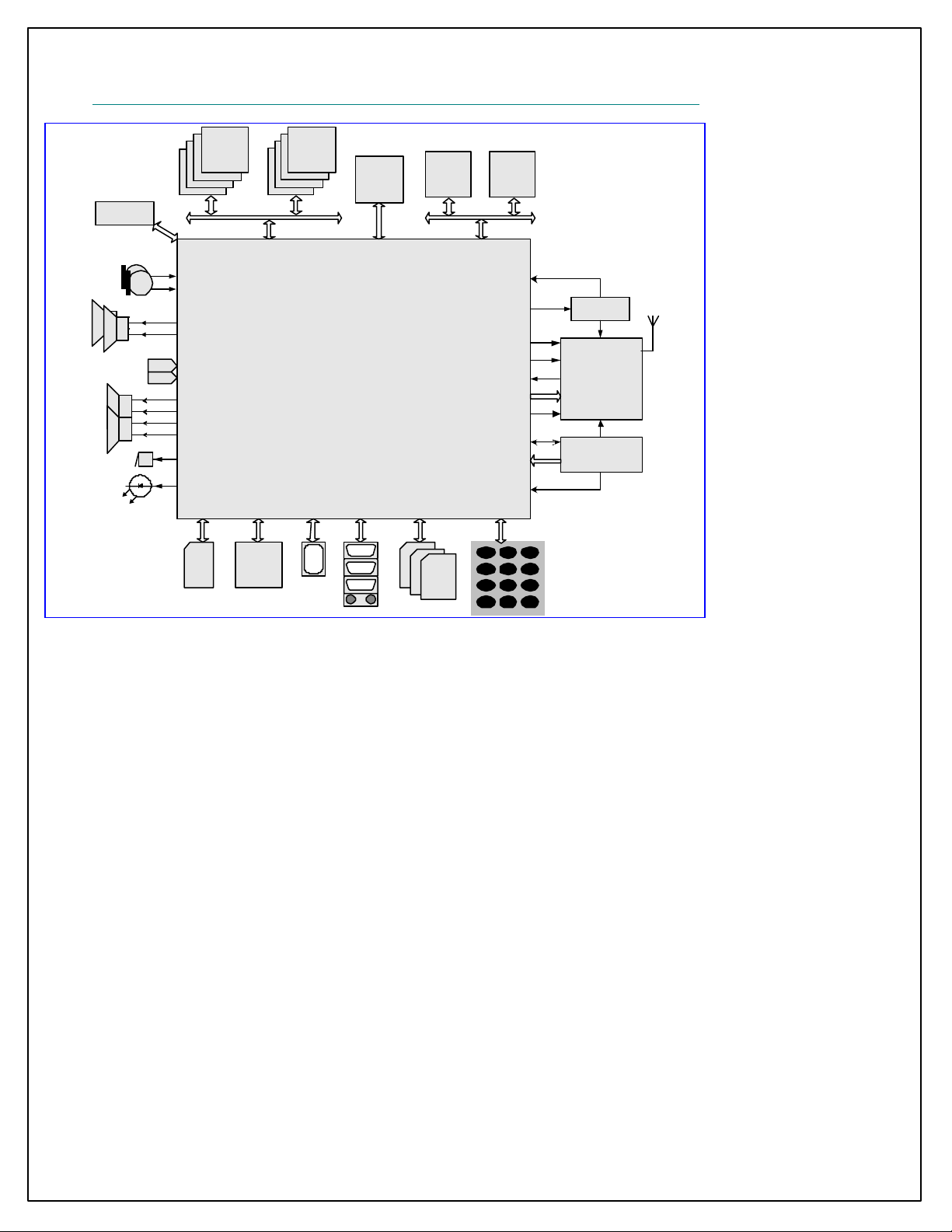
Typical application is shown in Figure 1.
Multi-media Subsystem
The MT6219 multi-media subsystem provides connection
to CMOS image sensor and supports resolution up to 1.3M
pixels. With it s advanced image signal and data processing
technology, MT6219 allows efficient processing of image
and video data. It also has built -in JPEG CODEC and
MPEG-4 CODEC, thus enabling real -time creation and
playback of high -quality images and video. In addition to
advanced image and video features, MT6219 also utilizes
high resolution DAC, digital audio, and audio synthesis
technology to provide superior audio features for all future
multi -media needs.
In order to provide more flexibility and bandwidth for
multi -media products, an additional 8-bit parallel interface
is incorporated. This interface ena bles connection to LCD
panels as well as connection to NAND flash devices to
allow for multi- media data storage capabilities.
External Memory Interface
Providing the greatest capacity for expansion, MT6219
supports up to 8 state-of-the-art devices through its 16-bit
host interface. Devices such as burst/page mode Flash,
page mode SRAM, Pseudo SRAM, Color/Parallel LCD,
and multi-media companion chip are all supported through
this interface. To minimize power consumption and ensure
low noise, this interface is designed for flexible I/O voltage
and allows lowering of supply voltage down to 1.8V. The
driving strength is configurable for signal integrity
adjustment. The data bus also employs retention
technology to prevent the bus from floating during turn
over.
7/ 418 MediaTek Inc. Confidential
User Interface
To provide complete user interface, MT6219 brings
together all the necessary peripheral blocks for
multi-media GSM /GPRS phone. The peripheral blocks
consists of the Keypad Scanner with the capability to
detect multiple key presses, SIM Controller, Alerter, Real
Time Clock, PWM, Serial LCD Controller, and General
Purpose Programmable I/Os. For connectivity and data
storage, the MT6219 supports UART, IrDA, USB 1.1
Slave and MMC/SD/MS/MS Pro. Furthermore, for large
amount of data transfer, high performance DMA (Direct
Memory Access) and hardware flow control are
implemented, which greatly enhances the performance and
reduces MCU processing load.
Audio Interface
Using a highly integrated mixed-signal Audio Front-End,
the MT6219 architecture allows for easy audio interfacing
with direct connection to the audio transducers. The audio
interface integrates D/A and A/D Converters for Voice
band, as well as high resolution Stereo D/A Converters for
Audio band. In addition, MT6219 also provides Stereo
Input and Analog Mux. Overall, MT6219’s audio features
provide a rich platform for multi-media applications.
Radio Interface
MT6219 integrates a mixed-signal Baseband front -end in
order to provide a well-organized radio interface with
flexibility for efficient customization. It contains gain and
offset calibration mechanisms, and filters with
programmable coefficients for comprehensive
compatibility control on RF modules. This approach also
allows the usage of a high resolution D/A Converter for
controlling VCXO or crystal, thus reducing the need for
expensive TCVCXO . MT6219 achieves great MODEM
performance by utilizing 14-bit high resolution A/D
Converter in the RF downlink path. Furthermore, to reduce
the need for extra external current -driving component, the
driving strength of some BPI outputs is designed to be
configurable.
Debug Function
Page 8

MT6219 GSM/GPRS Baseband Processor Data Sheet Revision 1.01
The JTAG interface enables in-circuit debugging of
software program with the ARM7EJ-S core. With this
standardized debugging interface, the MT6219 provides
developers with a wide set of options in choosing ARM
development kits from different third party vendors.
Power Management
The MT6219 offers various low-power features to help
reduce system power consumption. These features include
Pause Mode of 32KHz clocking at Standby State, Power
Down Mode for individual peripherals, and Processor
Sleep Mode. In addition, MT6219 is also fabricated in
advanced low leakage CMOS process, hence providing an
overall ultra low leakage solution.
Package
The MT6219 device is offered in a 13mm×13mm, 293-ball,
0.65 mm pitch, TFBGA package.
8/ 418 MediaTek Inc. Confidential
Page 9
MT6219 GSM/GPRS Baseband Processor Data Sheet Revision 1.01
FLASH
SRAM
PSRAM
DEBUGGER
JTAG
SPEECH/AUDIO
INPUT
SPEECH/AUDIO
OUTPUT
FM STEREO
RADIO INPUT
HIFI STEREO
OUTPUT
ALERTER
PWM
SIM
EXTERNAL MEMORY
INTERFACE
SERIAL
LCD
SERIAL
LCD
Figure 1 Typical application of MT6219
MELODY
LCD
USB
SENSOR
IMAGE INPUT
MT6219
UART
IRDA
CMOS
MMC/SD/MS
MSPRO
NAND
FLASH
8-BIT PARALLEL
INTERFACE
LCD
SYSCLK
AFC
APC
TX I/Q
RX I/Q
BPI
BSI
B2PSI
AUXADC
SUPPLY
VOLTAGES
KEYPAD
1 2 3
4 5 6
7 8 9
0 #
*
TCVCXO
RF
MODULE
POWER
MANAGEMENT
CIRCUITRY
9/ 418 MediaTek Inc. Confidential
Page 10

MT6219 GSM/GPRS Baseband Processor Data Sheet Revision 1.01
1.1 MODEM Features
n General
l Integrated voice-band, audio -band and base-band
analog front ends
l TFBGA 13mm×13mm, 293-ball, 0.65 mm pitch
package
n MCU Subsystem
l ARM7EJ-S 32-bit RISC processor
l High performance multi-layer AMBA bus
l Java hardware acceleration for fast Java- based
games and applets
l Operating frequency: 26/52 MHz
l Dedicated DMA bus
l 14 DMA channels
l 512K Bytes zero-wait-state on-chip SRAM
l On-chip boot ROM for Factory Flash
Programming
l Watchdog timer for system crash recovery
l 2 sets of General Purpose Timer
l Circuit Switch Data coprocessor
l Division coprocessor
n External Memory Interface
l Supports up to 8 external devices
l Supports 8- bit or 16-bit memory components with
maximum size of up to 64M Bytes each
l Supports Flash and SRAM with Page Mode or
Burst Mode
l Supports Pseudo SRAM
l Industry standard Parallel LCD Interface
l Supports multi-media companion chips with 8/16
bits data width
l Flexible I/O voltage of 1.8V ~ 2.8V for memory
interface
10/418 MediaTek Inc. Confidential
l Configurable driving strength for memory
interface
n Audio and Modem CODEC
l Dial tone generation
l Voice Memo
l Noise Reduction
l Echo Suppression
l Advanced Sidetone Oscillation Reduction
l Digital sidetone generator with programmable
gain
l Two programmable acoustic compensation filters
l GSM/GPRS quad vocoders for adaptive multirate
(AMR), enhanced full rate (EFR), full rate (FR)
and half rate (HR)
l GSM channel coding, equalization and A5/1 and
A5/2 ciphering
l GPRS GEA and GEA2 ciphering
l Programmable GSM /GPRS Modem
l Packet Switched Data with CS1/CS2/CS3/CS4
coding schemes
l GSM Circuit Switch Data
l GPRS Class 12
n User Interfaces
l 6-row × 7-column keypad controller with
hardware scanner
l Supports multiple key presses for gaming
l SIM/USIM Controller with hardware T=0/T=1
protocol control
l 3 UART s with hardware flow control and speed up
to 921600 bps
l IrDA modulator/demodulator with hardware
framer
Page 11

MT6219 GSM/GPRS Baseband Processor Data Sheet Revision 1.01
l Real Time Clock (RTC) operating with a separate
power supply
l Serial LCD Interface with 8/9 bit format support
l General Purpose I/Os (GPIOs)
l 2 Sets of Pulse Width Modulation (PWM) Output
l Alerter Output with Enhanced PWM or PDM
l Six external interrupt lines
n Audio Interface and Audio Front End
l Two microphone inputs sharing one low noise
amplifier with programmable gain
l Two Voice power amplifiers with programmable
gain
l 2nd order Sigma-Delta A/D Converter for voice
uplink path
l D/A Converter for voice downlink path
l Supports half- duplex hands-free operation
l Compliant with GSM 03.50
n Radio Interface and Baseband Front End
l GMSK modulator with analog I and Q channel
outputs
l 10-Pin Baseband Parallel Interface (BPI) with
programmable driving strength
l Multi-band support
n Power Management
l Power Down Mode for analog and digital circuits
l Processor Sleep Mode
l Pause Mode of 32KHz clocking at Standby State
l 7-channel Auxiliary 10-bit A/D Converter for
charger and battery monitoring and photo sensing
n Test and Debug
l Built-in digital and analog loop back modes for
both Audio and Baseband Front-End
l DAI port complying with GSM Rec.11.10
l JTAG port for debugging embedded MCU
l 10-bit D/A Converter for uplink baseband I and Q
signals
l 14-bit high resolution A/D Converter for downlink
baseband I and Q signals
l Calibration mechanism of offset and gain
mismatch for baseband A/D Converter and D/A
Converter
l 10-bit D/A Converter for Automatic Power
Control
l 13-bit high resolution D/A Converter for
Automatic Frequency Control
l Programmable Radio RX filter
l 2 Channels Baseband Serial Interface (BSI) with
3-wire control
11/418 MediaTek Inc. Confidential
Page 12

MT6219 GSM/GPRS Baseband Processor Data Sheet Revision 1.01
1.2 Multi-Media Features
n LCD/NAND Flash Interface
l Dedicated 8-bit Parallel Interface, supports up to 3
external devices
l Hardware accelerated LCD Controller for display
l Dedicated LCD bus
l NAND Flash Controller for mass storages
n LCD Controller
l Supports simultaneous connection to up to 2
parallel LCD and 1 serial LCD panels
l Supports format: RGB332, RGB444, RGB565,
RGB666, RGB888
l Supports LCD panel maximum resolution up to
800x600 at 16bpp
l Supports hardware display rotation
l Capable of combining display memories with up to
4 blending layers
n Image Signal Processor
l 8/10 bit Bayer format image input
l Capable of processing image of size up to 1.3M
pixels
l Color Correction Matrix
l Gamma Correction
l Automatic Exposure Control
l Automatic White Balance Control
l Programmable AE/AWB windows
l Edge Enhancement Support
l Histogram Equalization Logic
l Horizontal and Vertical Sync Information on
Separate Pin
n JPEG Decoder
l ISO/IEC 10918-1 JPEG Baseline and Progressive
modes
12/418 MediaTek Inc. Confidential
l Supports all possible YUV formats, including
grayscale format
l Supports all DC/AC Huffman table parsing
l Supports all quantization table parsing
l Supports restart interval
l Supports SOS, DHT, DQT and DRI marker
parsing
l IEEE Std 1180 -1990 IDCT Standard Compliant
l Supports progressive image processing to
minimize storage space requirement
l Supports reload-able DMA for VLD stream
n JPEG Encoder
l ISO/IEC 10918 -1 JPEG baseline mode
l ISO/IEC 10918 -2 Compliance
l Supports YUV422 and grayscale formats
l Standard DC and AC Huffman tables
l Provides 4 levels of encode quality
n Image Data Processing
l High throughput hardware Resizer capable of
tailoring image to arbitrary size
l Horizontal scaling in averaging method
l Vertical scaling in bilinear method
l Simultaneous scaling for MPEG- 4 encode and
LCD display
l YUV and RGB color space conversion
l Pixel format transform
l Boundary padding
l Pixel processing: hue/saturation/intensity/color
adjustment, Gamma correction and
grayscale/invert/sepia-tone effects
l Programmable Spatial Filtering: Linear filter,
Non-linear filter and Multi-pass artistic effects
Page 13

MT6219 GSM/GPRS Baseband Processor Data Sheet Revision 1.01
l Hardware accelerated im age editing
n MPEG -4/H.263 CODEC
l Hardware Video CODEC
l ISO/IEC 14496-2 simple profile:
decode @ level 0/1/2/3
encode @ level 0
l Supported visual tools for decoder: I-VOP, P -VOP,
AC/DC prediction, 4-MV, Unrestricted MV, Error
Resilience, Short Header
l Error Resilience for decoder: Slice
Resynchronization, Data Partitioning, Reversible
VLC
l Supported visual tools for encoder: I-VOP, P -VOP,
Half-pel, DC prediction, Unrestricted MV,
Reversible VLC, Short Header
l Supports encoding motion vector of range up
to –64/+63.5 pixels
l ITU-T H.263 profile 0 @ level 10
l AAC/AMR/WB-AMR audio decode support
l AMR/WB-AMR audio encode support
n 2D Accelerator
l Rectangle fill
l BitBlt: multi-BitBlt without transform, 7 rotate,
mirror (transparent) BitBlt
l Alpha blending
l Line drawing: normal lin e, dotted line
l Font caching: normal font, Italic font
l Supports 16-bpp RGB565 and 8-bpp index color
modes
l Command queue with 32 levels
n Audio CODEC
l Wavetable synthesis with up to 64 tones
l Advanced wavetable synthesizer capable of
generating simulated stereo
l Wavetable including GM full set of 128
instruments and 47 sets of percussions
l PCM Playback and Record
l Digital Audio Playback
l High resolution D/A Converters for Stereo Audio
playback
l Stereo analog input for stereo audio source
l Analog mixers for Stereo Audio
l Stereo to Mono Conversion
n Connectivity
l Full-speed USB 1.1 Device
l Multi Media Card/Secure Digital Memory
Card/Memory Stick/Memory Stick Pro host
controller
13/418 MediaTek Inc. Confidential
Page 14

MT6219 GSM/GPRS Baseband Processor Data Sheet Revision 1.01
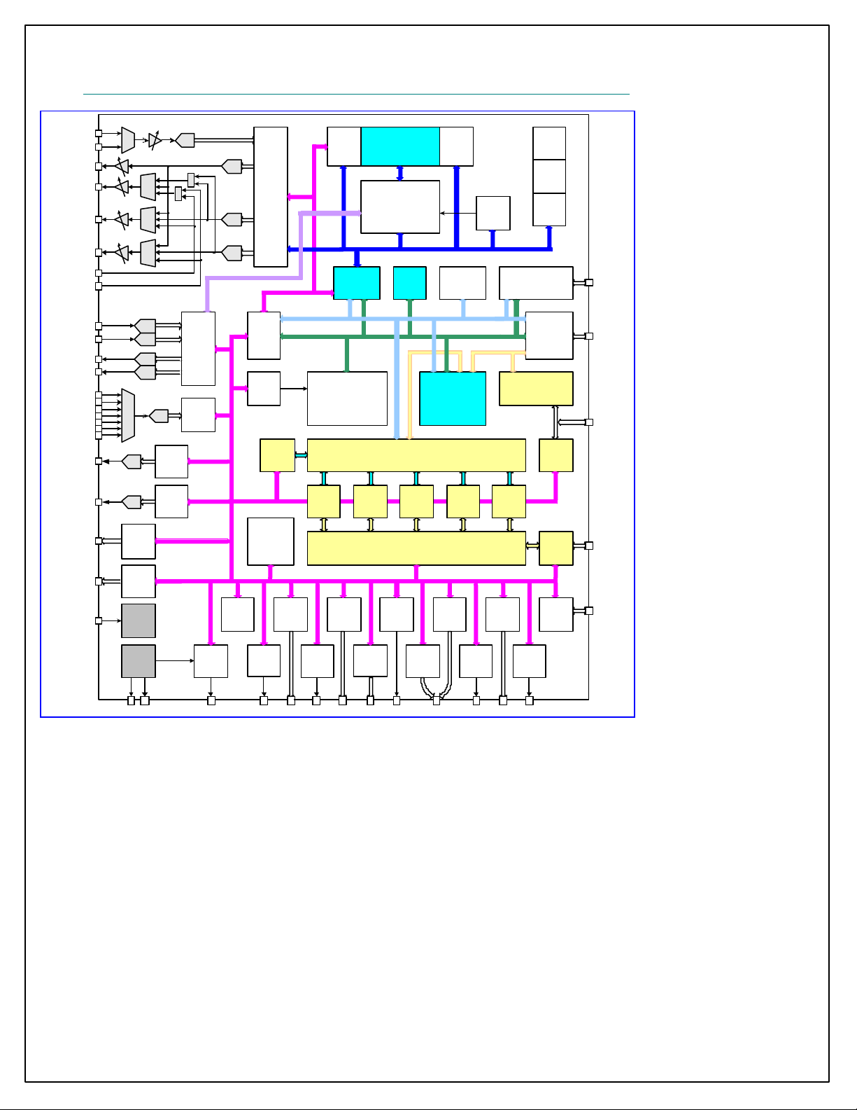
1.3 General Description
Figure 2 details the block diagram of MT6219. Based on a dual-processor architecture, MT6219 integrates both an
ARM7EJ-S core and a digital signal processor core. ARM7EJ-S is the main processor that is responsible for running
high-level GSM/GPRS protocol software as well as multi-media applications. The digital signal processor handles the
low-level MODEM as well as advanced audio functions. Except for some mixed- signal circuitries, the other building
blocks in MT6219 are connected to either the microcontroller or the digital signal processor.
Specifically, MT6219 consists of the following subsystems:
l Microcontroller Unit (MCU) Subsystem - includes an ARM7EJ-S RISC processor and its accompanying memory
management and interrupt handling logics.
l Digital Signal Processor (DSP) Subsystem - includes a DSP and its accompanying memory, memory controller,
and interrupt controller.
l MCU/DSP Interface - where the MCU and the DSP exchange hardware and software information.
l Microcontroller Peripherals - includes all user interface modules and RF control interface modules.
l Microcontroller Coprocessors - runs computing-intensive processes in place of Microcontroller.
l DSP Peripherals - hardware accelerators for GSM /GPRS channel codec.
l Multi-media Subsystem - integrates several advanced accelerators to support multi-media applications.
l Voice Front End - the data path for converting analog speech from and to digital speech.
l Audio Front End - the data path for converting stereo audio from stereo audio source
l Baseband Front End - the data path for converting digital signal from and t o analog signal of RF modules.
l Timing Generator - generat es the control signals related to the TDMA frame timing.
l Power, Reset and Clock subsystem - manages the power, reset , and clock distribution inside MT6219.
Details of the individual subsystems and blocks are described in following Chapters.
14/418 MediaTek Inc. Confidential
Page 15
MT6219 GSM/GPRS Baseband Processor Data Sheet Revision 1.01
MELODY
MIC-0
MIC-1
VOICE-0
VOICE-1
AUDIO-L
AUDIO-R
STEREO-L
STEREO-R
SERIAL RF
CONTROL
PARALLEL
RF CONTROL
RX-I
RX-Q
TX-I
TX-Q
AUX
ADC
AFC
APC
ADC
ADC
DAC
DAC
ADC
DAC AFC
DAC APC
BSI
BPI
ADC
+
BASEBAND
+
PATH
AUX
ADC
DAC
DAC
DAC
AUDIO
PATH
BRIDGE
INTERRUPT
CONTROL
2D ENGINE
TDMA
TIMER
IMAGE
DMA
PATCH
UNIT
MCU/DSP
INTERFACE
ARM7EJ-S
IMAGE
ENGINE
MEMORY
DSP
BOOT
ROM
GRAPHIC MEMORY
CONTROLLER
GIF
DECODER
IMAGE RESIZER
TRAP
UNIT
CONTROL
ON-CHIP
SRAM
CODEC
DMA
JPEG
INTERRUPT
CONTROL
MPEG-4
VIDEO
CODEC
DSP CO-
PROCESSOR
DSP CO-
PROCESSOR
DSP CO-
PROCESSOR
USB
EXTERNAL
MEMORY
INTERFACE
LCD
CONTROLLER
PROCESSOR
NAND
FLASH
INTERFACE
IMAGE
SIGNAL
USB
FLASH
SRAM
PSRAM
LCD
NAND
LCD
CMOS
SENSOR
SYSTEM
CLOCK
13/26MHZ
CLOCK
GEN
32K
OSC
32KHZ CRYSTAL
GPT
RTC
WAKE UP USER INTERFACERESET
WDT
SIM GPIO
PWM
KEYPAD
SCANNER
ALERTER
SERIAL
LCD
B2PSI IRDA
MMC
SD/MS
MS PRO
CONNECTIVITYSERIAL PORT
SCCB
UART
MT6219
Figure 2 MT6219 block diagram.
15/418 MediaTek Inc. Confidential
Page 16

MT6219 GSM/GPRS Baseband Processor Data Sheet Revision 1.01
2 Product Description
2.1 Pin Outs
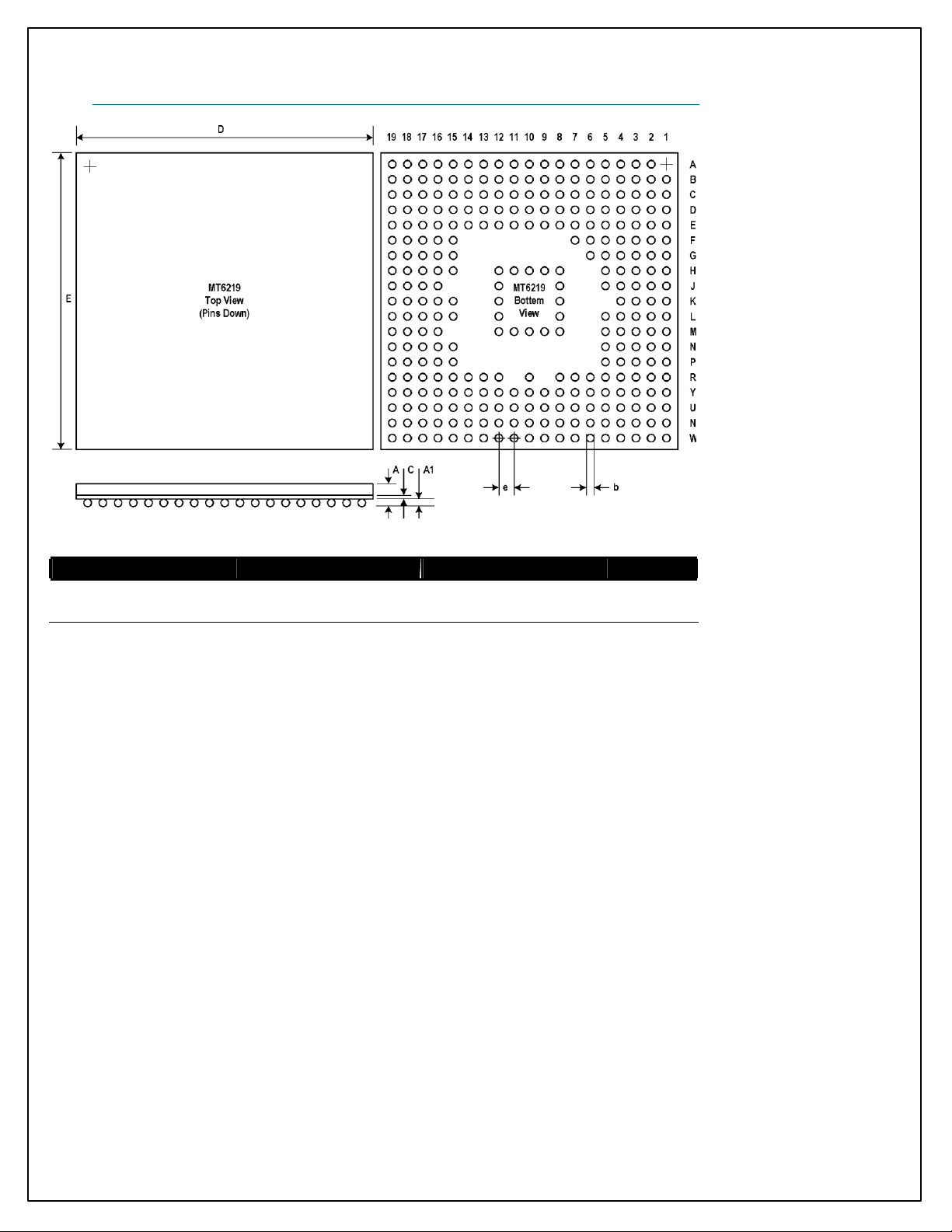
One type of package for this product, TFBGA 13mm*13mm , 293-ball, 0.65 mm pitch Package, is offered.
Pin outs and the top view are illustrated in Figure 3 for this package . Outline and dimension of package is illustrated in
Figure 4, while the definition of package is shown in Table 1.
16/418 MediaTek Inc. Confidential
Page 17

MT6219 GSM/GPRS Baseband Processor Data Sheet Revision 1.01
Figure 3 Top View of MT6219 TFBGA 13mm*13mm , 293-ball, 0.65 mm pitch Package
17/418 MediaTek Inc. Confidential
Page 18
MT6219 GSM/GPRS Baseband Processor Data Sheet Revision 1.01
Figure 4 Outlines and Dimension of TFBGA 13mm*1 3mm, 293-ball, 0.65 mm pitch Package
Body Size Ball Count Ball Pitch Ball Dia. Package Thk. Stand Off Substrate Thk.
D E N e b A (Max.) A1 C
13 13 293 0.65 0.35 1.4 0.3 0.36
Table 1 Definition of TFBGA 13mm*13mm, 293-ball, 0.65 mm pitch Package (Unit: mm)
18/418 MediaTek Inc. Confidential
Page 19
MT6219 GSM/GPRS Baseband Processor Data Sheet Revision 1.01
2.2 Pin Description
Ball
Name Dir Description
13X13
JTAG Port
E4 JTRST# I JTAG test port reset input PD Input
E3 JTCK I JTAG test port clock input PU Input
E2 JTDI I JTAG test port data input PU Input
E1 JTMS I JTAG test port mode swit ch PU Input
F5 JTDO O JTAG test port data output 0
F4 JRTCK O JTAG test port returned clock output 0
RF Parallel Control Unit
F3 BPI_BUS0 O RF hard-wire control bus 0 0
F2 BPI_BUS1 O RF hard-wire control bus 1 0
G5 BPI_BUS2 O RF hard- wire control bus 2 0
G4 BPI_BUS3 O RF hard- wire control bus 3 0
G3 BPI_BUS4 IO RF hard-wire control bus 4 Input
G2 BPI_BUS5 IO RF hard-wire control bus 5 Input
G1 BPI_BUS6 IO RF hard-wire control bus 6 GPIO10 BPI_BUS6 PD Input
H5 BPI_BUS7 IO RF hard-wire control bus 7 GPIO11 BPI_BUS7 PD Input
H4 BPI_BUS8 IO RF hard-wire control bus 4 GPIO12 BPI_BUS8 13MHz 32KHz PD Input
H3 BPI_BUS9 IO RF hard-wire control bus 5 GPIO13 BPI_BUS9 BSI_CS1 PD Input
RF Serial Control Unit
H1 BSI_CS0 O RF 3-wire interface chip select 0 0
J5 BSI_DATA O RF 3-wire interface data output 0
J4 BSI_CLK O RF 3-wire interface clock output 0
PWM Interface
R3 PWM1 IO Pulse width modulated signal 1 GPIO21 PWM1 DSP_GPO0 TBTXFS PD Input
R2 PWM2 IO Pulse width modulated signal 2 GPIO22 PWM2 DSP_GPO1 TBRXEN PD Input
T4 ALERTER IO Pulse width modulated signal for buzzer GPIO23 ALERTER DSP_GPO2 BTRXFS PD Input
Serial LCD/PM IC Interface
J3 LSCK IO Serial display interface data output GPIO16 LSCK TDMA_CK TBTXEN PD Input
J2 LSA0 IO Serial display interface address output GPIO17 LSA0 TDMA_D1 TDTIRQ PD Input
J1 LSDA IO Serial display interface clock output GPIO18 LSDA TDMA_D0 TCTIRQ2 PD Input
K4 LSCE0# IO Serial display interface chip select 0
output
K3 LSCE1# IO Serial display interface chip select 1
output
Parallel LCD/Nand-Flash Interface
K2 LPCE1# IO Parallel display interface chip select 1
output
L5 LPCE0# O Parallel display interface chip select 0
output
L4 LRST# O Parallel display interface Reset Signal 1
L3 LRD# O Parallel display interface Read Strobe 1
L2 LPA0 O Parallel display interface address output 1
L1 LWR# O Parallel display interface Write Strobe 1
M5 NLD7 IO Parallel LCD/Nand-Flash Data 7 PD Input
Mode0 Mode1 Mode2 Mode3
GPIO19 LSCE0# TDMA_FS TCTIRQ1 PU Input
GPIO20 LSCE1# LPCE2# TEVTVAL PU Input
GPIO24 LPCE1# DSP_TID0 MCU_TD0 PU Input
PU Input
PU/
PD
Rese
t
19/418 MediaTek Inc. Confidential
Page 20
MT6219 GSM/GPRS Baseband Processor Data Sheet Revision 1.01
M4 NLD6 IO Parallel LCD/Nand-Flash Data 6 PD Input
M3 NLD5 IO Parallel LCD/Nand-Flash Data 5 PD Input
N5 NLD4 IO Parallel LCD/Nand-Flash Data 4 PD Input
N4 NLD3 IO Parallel LCD/Nand-Flash Data 3 PD Input
N3 NLD2 IO Parallel LCD/Nand-Flash Data 2 PD Input
N2 NLD1 IO Parallel LCD/Nand-Flash Data 1 PD Input
N1 NLD0 IO Parallel LCD/Nand-Flash Data 0 PD Input
P5 NRNB IO Nand-Flash Read/Busy Flag GPIO25 NRNB DSP_TID1 MCU_TID1 PU Input
P4 NCLE IO Nand-Flash Command Latch Signal GPIO26 NCLE DSP_TID2 MCU_TID2 PD Input
P3 NALE IO Nand-Flash Address Latch Signal GPIO27 NALE DSP_TID3 MCU_TID3 PD Input
P2 NWE# IO Nand-Flash Write Strobe GPIO28 NWE# DSP_TID4 MCU_DID PU Input
P1 NRE# IO Nand-Flash Read Strobe GPIO29 NRE# DSP_TID5 MCU_DFS PU Input
R4 NCE# IO Nand-Flash Chip select output GPIO30 NCE# DSP_TID6 MCU_DCK PU Input
SIM Card Interface
L18 SIMRST O SIM card reset output 0
L17 SIMCLK O SIM card clock output 0
K15 SIMVCC O SIM card supply power control 0
K16 SIMSEL O SIM card supply power select GPIO32 SIMSEL PD Input
K17 SIMDATA IO SIM card data input/output 0
Dedicated GPIO Interface
U2 GPIO0 IO General purpose input/output 0 GPIO0 DSP_GPO3 PD Input
M19 GPIO1 IO General purpose input/output 1 GPIO1 DICK PD Input
L15 GPIO2 IO General purpose input/output 2 GPIO2 DID PD Input
L16 GPIO3 IO General purpose input/output 3 GPIO3 DIMS PD Input
C17 GPIO4 IO General purpose input/output 4 GPIO4 DSP_CLK DSPLCK TRASD4 PD Input
A19 GPIO5 IO General purpose input/output 5 GPIO5 AHB_CLK DSPLD3 TRASD3 PD Input
B18 GPIO6 IO General purpose input/output 6 GPIO6 ARM_CLK DSPLD2 TRASD2 PD Input
B17 GPIO7 IO General purpose input/output 7 GPIO7 SLOW_CK DSPLD1 TRASD1 PD Input
A18 GPIO8 IO General purpose input/output 19 GPIO8 SCL DSPLD0 TRASD0 PD Input
A17 GPIO9 IO General purpose input/output 21 GPIO9 SDA DSPLSYNC TRARSY
NC
Miscellaneous
U1 SYSRST# I System reset input active low Input
R18 WATCHDOG# O Watchdog reset output 1
PD Input
T3 SRCLKENAN O External TCXO enable output active
low
T1 SRCLKENA O External TCXO enable output active
high
T2 SRCLKENAI IO External TCXO enable input GPIO31 SRCLKEN
E5 IBOOT I Boot Device Configuration Input PD Input
Keypad Interface
G17 KCOL6 I Keypad column 6 PU Input
G18 KCOL5 I Keypad column 5 PU Input
20/418 MediaTek Inc. Confidential
GPO1 SRCLKEN
AN
GPO0 SRCLKENA 1
AI
0
PD Input
Page 21
MT6219 GSM/GPRS Baseband Processor Data Sheet Revision 1.01
G19 KCOL4 I Keypad column 4 PU Input
F15 KCOL3 I Keypad column 3 PU Input
F16 KCOL2 I Keypad column 2 PU Input
F17 KCOL1 I Keypad column 1 PU Input
F18 KCOL0 I Keypad column 0 PU Input
F19 KROW5 O Keypad row 5 0
E16 KROW4 O Keypad row 4 0
E17 KROW3 O Keypad row 3 0
E18 KROW2 O Keypad row 2 0
D16 KROW1 O Keypad row 1 0
D19 KROW0 O Keypad row 0 0
External Interrupt Interface
V1 EINT0 I External interrupt 0 PU Input
U3 EINT1 I External interrupt 1 PU Input
W1 EINT2 I External interrupt 2 PU Input
V2 EINT3 I External interrupt 3 PU Input
R5 MIRQ I Interrupt to MCU GPIO41 MIRQ 13MHz 32KHz PU Input
R17 MFIQ I Interrupt to MCU GPIO42 MFIQ PU Input
External Memory Interface
R16 ED0 IO External memory data bus 0 Input
R15 ED1 IO External memory data bus 1 Input
T19 ED2 IO External memory data bus 2 Input
T17 ED3 IO Ext ernal memory data bus 3 Input
U19 ED4 IO External memory data bus 4 Input
U18 ED5 IO External memory data bus 5 Input
V18 ED6 IO External memory data bus 6 Input
W19 ED7 IO External memory data bus 7 Input
U17 ED8 IO External memory data bus 8 Input
V17 ED9 IO External memory data bus 9 Input
W17 ED10 IO External memory data bus 10 Input
T16 ED11 IO External memory data bus 11 Input
W16 ED12 IO External memory data bus 12 Input
T15 ED13 IO External memory data bus 13 Input
U15 ED14 IO External memory data bus 14 Input
V15 ED15 IO External memory data bus 15 Input
U14 ERD# O External memory read strobe 1
W14 EWR# O External memory write strobe 1
R13 ECS0# O External memory chip select 0 1
T13 ECS1# O External memory chip select 1 1
U13 ECS2# O External memory chip select 2 1
V13 ECS3# O External memory chip select 3 1
R12 ECS4# O External memory chip select 4 GPIO54 ECS4# PU 1
T12 ECS5# O External memory chip select 5 GPIO53 ECS5# PU 1
U12 ECS6# O External memory chip select 6 GPIO52 ECS6# PU 1
W12 ECS7# O External memory chip select 7 GPIO40 ECS7# PU 1
R14 ELB# O External memory lower byte strobe 1
T14 EUB# O External memory upper byte strobe 1
T11 EPDN# O Power Down Control Signal for
PSRAM
21/418 MediaTek Inc. Confidential
GPO2 EPDN# 0
Page 22
MT6219 GSM/GPRS Baseband Processor Data Sheet Revision 1.01
U11 EADV# O Address valid for burst mode flash
memory
V11 ECLK O Clock for flash memory 0
R10 EA0 O External memory address bus 0 0
T10 EA1 O External memory address bus 1 0
U10 EA2 O External memory address bus 2 0
W10 EA3 O External memory address bus 3 0
T9 EA4 O External memory address bus 4 0
U9 EA5 O External memory address bus 5 0
V9 EA6 O External memory address bus 6 0
R8 EA7 O External memory address bus 7 0
T8 EA8 O External memory address bus 8 0
W8 EA9 O External memory address bus 9 0
R7 EA10 O External memory address bus 10 0
T7 EA11 O External memory address bus 11 0
U7 EA12 O External memory address bus 12 0
V7 EA13 O External memory address bus 13 0
R6 EA14 O External memory address bus 14 0
T6 EA15 O External memory address bus 15 0
U6 EA16 O External memory address bus 16 0
W6 EA17 O External memory address bus 17 0
T5 EA18 O External memory address bus 18 0
U5 EA19 O External memory address bus 19 0
V5 EA20 O External memory address bus 20 0
W5 EA21 O External memory address bus 21 0
V4 EA22 O External memory address bus 22 0
U4 EA23 O External memory address bus 23 0
W3 EA24 O External memory address bus 24 GPO3 EA24 0
W2 EA25 O External memory address bus 25 GPO4 EA25 13MHz 32KHz 0
USB Interface
P16 USB_DP IO USB D+ Input/Output
P17 USB_DM IO USB D- Input/Output
Memory Card Interface
P19 MCCM0 IO SD Command/MS Bus State Output
N15 MCDA0 IO SD Serial Data IO 0/MS Serial Data IO
N16 MCDA1 IO SD Serial Data IO 1
N17 MCDA2 IO SD Serial Data IO 2
N18 MCDA3 IO SD Serial Data IO 3
N19 MCCK O SD Serial Clock/MS Serial Clock
Output
M16 MCPWRON O SD Power On Control Output
M17 MCWP I SD Write Protect Input GPIO15 MCWP PU
M18 MCINS I SD Card Detect Input GPIO14 MCINS PU
UART Interface
K18 URXD1 I UART 1 receive data PU Input
K19 UTXD1 O UART 1 transmit data 1
J16 UCTS1 I UART 1 clear to send PU Input
J17 URTS1 O UART 1 request to send 1
J18 URXD2 IO UART 2 receive data GPIO35 URXD2 UCTS3 PU Input
22/418 MediaTek Inc. Confidential
1
Page 23
MT6219 GSM/GPRS Baseband Processor Data Sheet Revision 1.01
J19 UTXD2 IO UART 2 transmit data GPIO36 UTXD2 URTS3 PU Input
H15 URXD3 IO UART 3 receive data GPIO33 URXD3 PU Input
H16 UTXD3 IO UART 3 transmit data GPIO34 UTXD3 PU Input
H17 IRDA_RXD IO IrDA receive data GPIO37 IRDA_RXD UCTS2 PU Input
G15 IRDA_TXD IO IrDA transmit data GPIO38 IRDA_TXD URTS2 PU Input
G16 IRDA_PDN IO IrDA Power Down Control GPIO39 IRDA_PDN PU Input
Digital Audio Interface
D17 DAICLK IO DAI clock output GPIO43 DAICLK DSPLD7 TRACLK PU Input
D18 DAIPCMOUT IO DAI pcm data out GPIO44 DAIPCMO
C19 DAIPCMIN IO DAI pcm data input GPIO45 DAIPCMIN DSPLD5 TRASD7 PU Input
C18 DAIRST IO DAI reset signal input GPIO47 DAIRST DSPLD4 TRASD6 PU Input
B19 DAISYNC IO DAI frame synchronization signal
CMOS Sensor Interface
J12 CMRST IO CMOS sensor reset signal output GPIO48 CMRST Z Input
K12 CMPDN IO CMOS sensor power down control GPIO49 CMPDN Z Input
H12 CMVREF I Sensor vertical refe rence signal input Input
H11 CMHREF I Sensor horizontal reference signal input Input
H9 CMPCLK I CMOS sensor pixel clock input Input
H10 CMMCLK O CMOS sensor master clock output Outp
H8 CMDAT9 I CMOS sensor data input 9 Input
J8 CMDAT8 I CMOS sensor data input 8 Input
K8 CMDAT7 I CMOS sensor data input 7 Input
L8 CMDAT6 I CMOS sensor data input 6 Input
M8 CMDAT5 I CMOS sensor data input 5 Input
M9 CMDAT4 I CMOS sensor data input 4 Input
M10 CMDAT 3 I CMOS sensor data input 3 Input
M11 CMDAT2 I CMOS sensor data input 2 Input
M12 CMDAT1 IO CMOS sensor data input 1 GPIO50 CMDAT1 PD Input
L12 CMDAT0 IO CMOS sensor data input 0 GPIO51 CMDAT2 PD Input
Analog Interface
B15 AU_MOUL Audio analog output left channel
A15 AU_MOUR Audio analog output right channel
C14 AU_M_BYP Audio DAC bypass pin
B14 AU_FMINL FM radio analog input left channel
A14 AU_FMINR FM radio analog input right channel
D13 AU_OUT1_P Earphone 1 amplifier output (+)
C13 AU_OUT1_N Earphone 1 amplifier output (-)
B12 AU_OUT0_N Earphone 0 amplifier output (-)
A12 AU_OUT0_P Earphone 0 amplifier output (+)
C12 AU_MICBIA
S_P
D12 AU_MICBIA
S_N
output
Microphone bias supply (+)
Microphone bias supply (-)
GPIO46 DAISYNC BFEPRBO TRASD5 PU Input
UT
DSPLD6 TRASYNC PD Input
ut
23/418 MediaTek Inc. Confidential
Page 24
MT6219 GSM/GPRS Baseband Processor Data Sheet Revision 1.01
C11 AU_VREF_N Audio reference voltage (-)
B11 AU_VREF_P Audio reference voltage (+)
D10 AU_VIN0_P Microphone 0 amplifier input (+)
C10 AU_VIN0_N Microphone 0 amplifier input (-)
B10 AU_VIN1_N Microphone 1 amplifier input (-)
A10 AU_VIN1_P Microphone 1 amplifier input (+)
D9 BDLAQP Quadrature input (Q+) baseband codec
downlink
C9 BDLAQN Quadrature input (Q-) baseband codec
downlink
A9 BDLAIN In-phase input (I+) baseband codec
downlink
B9 BDLAIP In-phase input (I-) baseband codec
downlink
B8 BUPAIP In-phase output (I+) baseband codec
uplink
A8 BUPAIN In-phase output (I-) baseband codec
uplink
C8 BUPAQN Quadrature output (Q+) baseband codec
uplink
D8 BUPAQP Quadrature output (Q-) baseband codec
uplink
B7 APC Automatic power control DAC output
D6 AUXADIN0 Auxiliary ADC input 0
C6 AUXADIN1 Auxiliary ADC input 1
B6 AUXADIN2 Auxiliary ADC input 2
A6 AUXADIN3 Auxiliary ADC input 3
C5 AUXADIN4 Auxiliary ADC input 4
B5 AUXADIN5 Auxiliary ADC input 5
A5 AUXADIN6 Auxiliary ADC input 6
C4 AUX_REF Auxiliary ADC reference voltage input
B4 AFC Automatic frequency control DAC
output
A4 AFC_BYP Automatic frequency control DAC
bypass capacitance
VCXO Interface
A2 SYSCLK 13MHz or 26MHz system clock input
RTC Interface
C2 XIN 32.768 KHz crystal input
B1 XOUT 32.768 KHz crystal output
C1 BBWAKEUP O Baseband power on/off control 1
Supply Voltages
D1 VDDK Supply voltage of internal logic
M1 VDDK Supply voltage of internal logic
V8 VDDK Supply voltage of internal logic
V16 VDDK Supply voltage of internal logic
H19 VDDK Supply voltage of internal logic
C16 VDDK Supply voltage of internal logic
W4 VDD33_EMI Supply voltage of memory interface
driver
24/418 MediaTek Inc. Confidential
Page 25

MT6219 GSM/GPRS Baseband Processor Data Sheet Revision 1.01
W7 VDD33_EMI Supply voltage of memory interface
driver
W9 VDD33_EMI Supply voltage of memory interface
driver
W11 VDD33_EMI Supply voltage of memory interface
driver
W13 VDD33_EMI Supply voltage of memory interface
driver
W15 VDD33_EMI Supply voltage of memory interface
driver
W18 VDD33_EMI Supply voltage of memory interface
driver
T18 VDD33_EMI Supply voltage of memory interface
driver
V3 VSS33_EMI Ground of memory interface driver
V6 VSS33_EMI Ground of memory interface driver
U8 VSS33_EMI Ground of memory interface driver
V10 VSS33_EMI Ground of memory interface driver
V12 VSS33_EMI Ground of memory interface driver
V14 VSS33_EMI Ground of memory interface driver
U16 VSS33_EMI Ground of memory interface driver
V19 VSS33_EMI Ground of memory interface driver
R19 VSS33_EMI Ground of memory interface driver
P15 VDD33_USB Supply voltage of drivers for USB
D4 VDD33 Supply voltage of drivers exce pt
memory interface and USB
F1 VDD33 Supply voltage of drivers except
memory interface and USB
K1 VDD33 Supply voltage of drivers except
memory interface and USB
R1 VDD33 Supply voltage of drivers except
memory interface and USB
L19 VDD33 Supply voltage of drivers except
memory interface and USB
E19 VDD33 Supply voltage of drivers except
memory interface and USB
E15 VDD33 Supply voltage of drivers except
memory interface and USB
E13 VDD33 Supply voltage of drivers except
memory interface and USB
E11 VDD33 Supply voltage of drivers except
memory interface and USB
E6 VDD33 Supply voltage of drivers except
memory interface and USB
A3 VSS33 Ground of drivers except memory
interface
D2 VSS33 Ground of drivers except memory
interface
D5 VSS33 Ground of drivers except memory
interface
H2 VSS33 Ground of drivers except memory
interface
25/418 MediaTek Inc. Confidential
Page 26

MT6219 GSM/GPRS Baseband Processor Data Sheet Revision 1.01
M2 VSS33 Ground of drivers except memory
P18 VSS33 Ground of drivers except memory
H18 VSS33 Ground of drivers except memory
A16 VSS33 Ground of drivers except memory
B16 VSS33 Ground of drivers except memory
E14 VSS33 Ground of drivers except memory
E12 VSS33 Ground of drivers except memory
E7 VSS33 Ground of drivers except memory
B3 AVDD_PLL Supply voltage for PLL
C3 AVSS_PLL Ground for PLL supply
B2 AVDD_RTC Supply voltage for Real Time Clock
Analog Supplies
C15 AVDD_MBUF Supply Voltage for Audio band section
D14 AVSS_MBUF GND for Audio band section
B13 AVDD_BUF Supply voltage for voice band transmit
A13 AVSS_BUF GND for voice band transmit section
D11 AVDD_AFE Supply voltage for voice band receive
A11 AGND_AFE GND reference voltage for voice band
E10 AVSS_AFE GND for voice band receive section
E9 AGND_RFE GND reference voltage for baseband
E8 AVSS_GSMR
FTX
D7 AVDD_GSM
RFTX
C7 AVSS_RFE GND for baseband receive section,
A7 AVDD_RFE Supply voltage for baseband receive
interface
interface
interface
interface
interface
interface
interface
interface
section
section
section
section, APC, AFC and AUXADC
GND for baseband transmit section
Supply voltage for baseband transmit
section
APC, AFC and AUXADC
section, APC, AFC and AUXADC
Table 2 Pin Descriptions (Bolded types are functions at reset)
26/418 MediaTek Inc. Confidential
Page 27
MT6219 GSM/GPRS Baseband Processor Data Sheet Revision 1.01
2.3 Power Description
Ball
Name IO Supply IO GND Core Supply Core GND Remark
13X13
B17 GPIO7 VDDK VSSK
A18 GPIO8 VDDK VSSK
A17 GPIO9
B16 VSS33
A16 VSS33
C16 VDDK Typ. 1.2V
E15 VDD33 Typ. 2.8V
E14 VSS33
E13 VDD33 Typ. 2.8V
E12 VSS33
E11 VDD33 Typ. 2.8V
E7 VSS33
E6 VDD33 Typ. 2.8V
D5 VSS33
J12 CMRST VDDK VSSK
K12 CMPDN VDDK VSSK
H12 CMVREF VDDK VSSK
H11 CMHREF VDDK VSSK
H9 CMPCLK VDDK VSSK
H10 CMMCLK
D4 VDD33 Typ. 2.8V
H8 CMDAT9 VDDK VSSK
J8 CMDAT8 VDDK VSSK
K8 CMDAT7 VDDK VSSK
L8 CMDAT6 VDDK VSSK
M8 CMDAT5 VDDK VSSK
M9 CMDAT4 VDDK VSSK
M10 CMDAT3 VDDK VSSK
M11 CMDAT2 VDDK VSSK
M12 CMDAT1 VDDK VSSK
L12 CMDAT0
A3 VSS33
B3 AVDD_PLL Typ. 2.8V
A2 SYSCLK AVDD_PLL AVSS_PLL AVDD_PLL AVSS_PLL
C3 AVSS_PLL
B2 AVDD_RTC Typ. 1. 2V
B1 XOUT AVDD_RTC VSS33 AVDD_RTC VSS33
C2 XIN AVDD_RTC VSS33 AVDD_RTC VSS33
C1 BBWAKEUP AVDD_RTC VSS33 AVDD_RTC VSS33
D2 VSS33
D3 TESTMODE VDD33 VSS33 VDDK VSSK
D1 VDDK Typ. 1.2V
E5 IBOOT VDDK VSSK
E4 JTRST#
VDD33 VSS33
VDDK VSSK
VDD33 VSS33
VDDK VSSK
VDD33 VSS33
VDDK VSSK
VDD33 VSS33
VDDK VSSK
27/418 MediaTek Inc. Confidential
Page 28
MT6219 GSM/GPRS Baseband Processor Data Sheet Revision 1.01
E3 JTCK VDDK VSSK
E2 JTDI VDDK VSSK
E1 JTMS VDDK VSSK
F5 JTDO VDDK VSSK
F4 JRTCK VDDK VSSK
F3 BPI_BUS0 VDDK VSSK
F2 BPI_BUS1 VDDK VSSK
F1 VDD33 Typ. 2.8V
G5 BPI_BUS2 VDDK VSSK
G4 BPI_BUS3 VDDK VSSK
G3 BPI_BUS4 VDDK VSSK
G2 BPI_BUS5 VDDK VSSK
G1 BPI_BUS6 VDDK VSSK
H5 BPI_BUS7 VDDK VSSK
H4 BPI_BUS8
H2 VSS33
H3 BPI_BUS9 VDDK VSSK
H1 BSI_CS0 VDDK VSSK
J5 BSI_DATA VDDK VSSK
J4 BSI_CLK VDDK VSSK
J3 LSCK VDDK VSSK
J2 LSA0 VDDK VSSK
J1 LSDA VDDK VSSK
K4 LSCE0# VDDK VSSK
K3 LSCE1#
K1 VDD33 Typ. 2.8V
K2 LPCE1# VDDK VSSK
L5 LPCE0# VDDK VSSK
L4 LRST# VDDK VSSK
L3 LRD# VDDK VSSK
L2 LPA0 VDDK VSSK
L1 LWR# VDDK VSSK
M5 NLD7 VDDK VSSK
M4 NLD6 VDDK VSSK
M3 NLD5
M2 VSS33
M1 VDDK Typ. 1.2V
N5 NLD4 VDDK VSSK
N4 NLD3 VDDK VSSK
N3 NLD2 VDDK VSSK
N2 NLD1 VDDK VSSK
N1 NLD0 VDDK VSSK
P5 NRNB VDDK VSSK
P4 NCLE VDDK VSSK
P3 NALE VDDK VSSK
P2 NEW# VDDK VSSK
P1 NRE# VDDK VSSK
R4 NCE#
R1 VDD33 Typ. 2.8V
28/418 MediaTek Inc. Confidential
VDD33 VSS33
VDDK VSSK
VDD33 VSS33
VDDK VSSK
VDD33 VSS33
VDDK VSSK
VDD33 VSS33
VDDK VSSK
Page 29
MT6219 GSM/GPRS Baseband Processor Data Sheet Revision 1.01
R3 PWM1 VDDK VSSK
R2 PWM2 VDDK VSSK
T4 ALERTER VDDK VSSK
T1 SRCLKENA VDDK VSSK
T3 SRCLKENAN VDDK VSSK
T2 SRCLKENAI VDDK VSSK
U1 SYSRST# VDDK VSSK
U2 GPIO0 VDDK VSSK
V1 EINT0 VDDK VSSK
U3 EINT1 VDDK VSSK
W1 EINT2 VDDK VSSK
V2 EINT3
V3 VSS33_EMI
W2 EA25 VDDK VSSK
W3 EA24 VDDK VSSK
U4 EA23 VDDK VSSK
V4 EA22
W4 VDD33_EMI Typ. 1.8~2.8V
R5 MIRQ VDDK VSSK
W5 EA21 VDDK VSSK
V5 EA20 VDDK VSSK
U5 EA19 VDDK VSSK
T6 EA18
V6 VSS33_EMI
W6 EA17 VDDK VSSK
U6 EA16 VDDK VSSK
T6 EA15 VDDK VSSK
R6 EA14
W7 VDD33_EMI Typ. 1.8~2.8V
V7 EA13 VDDK VSSK
U7 EA12 VDDK VSSK
T7 EA11 VDDK VSSK
R7 EA10
V8 VDDK Typ. 1.2V
U8 VSS33_EMI
W8 EA9 VDDK VSSK
T8 EA8 VDDK VSSK
R8 EA7 VDDK VSSK
V9 EA6
W9 VDD33_EMI Typ. 1.8~2.8V
U9 EA5 VDDK VSSK
T9 EA4 VDDK VSSK
W10 EA3
V10 VSS33_EMI
U10 EA2 VDDK VSSK
T10 EA1 VDDK VSSK
R10 EA0
W11 VDD33_EMI Typ. 1.8~2.8V
29/418 MediaTek Inc. Confidential
VDD33 VSS33
VDDK VSSK
VDD33_EMI VSS33_EMI
VDDK VSSK
VDD33_EMI VSS33_EMI
VDDK VSSK
VDD33_EMI VSS33_EMI
VDDK VSSK
VDD33_EMI VSS33_EMI
VDDK VSSK
VDD33_EMI VSS33_EMI
VDDK VSSK
VDD33_EMI VSS33_EMI
VDDK VSSK
VDD33_EMI VSS33_EMI
VDDK VSSK
Page 30
MT6219 GSM/GPRS Baseband Processor Data Sheet Revision 1.01
U11 EADV# VDDK VSSK
V11 ECLK VDDK VSSK
T11 EPDN#
V12 VSS33_EMI
W12 ECS7# VDDK VSSK
U12 ECS6# VDDK VSSK
T12 ECS5# VDDK VSSK
R12 ECS4#
W13 VDD33_EMI Typ. 1.8~2.8V
V13 ECS3# VDDK VSSK
U13 ECS2# VDDK VSSK
T13 ECS1# VDDK VSSK
R13 ECS0#
V14 VSS33_EMI
W14 EWR# VDDK VSSK
U14 ERD# VDDK VSSK
T14 EUB# VDDK VSSK
R14 ELB#
W15 VDD33_EMI Typ. 1.8~2.8V
V15 ED15 VDDK VSSK
U15 ED14 VDDK VSSK
T15 ED13 VDDK VSSK
W16 ED12
V16 VDDK 1.2V
U16 VSS33_EMI
T16 ED11 VDDK VSSK
W17 ED10 VDDK VSSK
V17 ED9
W18 VDD33_EMI Typ. 1.8~2.8V
U17 ED8 VDDK VSSK
W19 ED7 VDDK VSSK
V18 ED6
V19 VSS33_EMI
U18 ED5 VDDK VSSK
U19 ED4 VDDK VSSK
T17 ED3
T18 VDD33_EMI Typ. 1.8~2.8V
T19 ED2 VDDK VSSK
R15 ED1 VDDK VSSK
R16 ED0 VDDK VSSK
R17 MFIQ VDDK VSSK
R18 WATCHDOG
R19 VSS33_EMI
P15 VDD33_USB Typ. 3.3V
P16 USB_DP VDDK VSSK
P17 USB_DM
P18 VSS33
P19 MCCM0 VDDK VSSK
N15 MCDA0
30/418 MediaTek Inc. Confidential
VDD33_EMI VSS33_EMI
VDD33_EMI VSS33_EMI
VDD33_EMI VSS33_EMI
VDD33_EMI VSS33_EMI
VDD33_EMI VSS33_EMI
VDD33_EMI VSS33_EMI
VDD33_EMI VSS33_EMI
VDD33_EMI VSS33_EMI
VDD33_EMI VSS33_EMI
VDD33_USB VSS33
VDD33
VSS33
VDDK VSSK
VDDK VSSK
VDDK VSSK
VDDK VSSK
VDDK VSSK
VDDK VSSK
VDDK VSSK
VDDK VSSK
VDDK VSSK
VDDK VSSK
VDDK VSSK
Page 31

MT6219 GSM/GPRS Baseband Processor Data Sheet Revision 1.01
N16 MCDA1 VDDK VSSK
N17 MCDA2 VDDK VSSK
N18 MCDA3 VDDK VSSK
N19 MCCK VDDK VSSK
M16 MCPWRON VDDK VSSK
M17 MCWP VDDK VSSK
M18 MCINS VDDK VSSK
M19 GPIO1 VDDK VSSK
L15 GPIO2 VDDK VSSK
L16 GPIO3 VDDK VSSK
L19 VDD33 Typ. 2.8V
L18 SIMRST VDDK VSSK
L17 SIMCLK VDDK VSSK
K15 SIMVCC VDDK VSSK
K16 SIMSEL VDDK VSSK
K17 SIMDATA VDDK VSSK
K18 URXD1 VDDK VSSK
K19 UTXD1 VDDK VSSK
J16 UCTS1 VDDK VSSK
J17 URTS1 VDDK VSSK
J18 URXD2 VDDK VSSK
J19 UTXD2 VDDK VSSK
H15 URXD3 VDDK VSSK
H16 UTXD3
H19 VDDK VDDK VSSK Typ. 1.2V
H18 VSS33 VDDK VSSK
H17 IRDA_PDN VDDK VSSK
G15 IRDA_TXD VDDK VSSK
G16 IRDA_RXD VDDK VSSK
G17 KCOL6 VDDK VSSK
G18 KCOL5 VDDK VSSK
G19 KCOL4 VDDK VSSK
F15 KCOL3 VDDK VSSK
F16 KCOL2 VDDK VSSK
F17 KCOL1 VDDK VSSK
F18 KCOL0 VDDK VSSK
F19 KROW5 VDDK VSSK
E16 KROW4 VDDK VSSK
E17 KROW3 V DDK VSSK
E18 KROW2
E19 VDD33 Typ. 2.8V
D16 KROW1 VDDK VSSK
D19 KROW0 VDDK VSSK
D17 DAICLK VDDK VSSK
D18 DAIPCMOUT VDDK VSSK
C19 DAIPCMIN VDDK VSSK
C18 DAIRST VDDK VSSK
B19 DAISYNC VDDK VSSK
C17 GPIO4
31/418 MediaTek Inc. Confidential
VDD33
VDD33
VDD33 VSS33
VSS33
VSS33
VDDK VSSK
VDDK VSSK
VDDK VSSK
Page 32

MT6219 GSM/GPRS Baseband Processor Data Sheet Revision 1.01
A19 GPIO5 VDDK VSSK
A18 GPIO6 VDDK VSSK
C15 AVDD_MBUF Typ. 2.8V
B15 AU_MOUTL
A15 AU_MOUTR
D14 AVSS_MBUF
C14 AU_M_BYP
B14 AU_FMINL
A14 AU_FMINR
D13 AU_OUT1_P
C13 AU_OUT1_N
B12 AU_OUT0_N
B13 AVDD_BUF Typ. 2.8V
A12 AU_OUT0_P
A13 AVSS_BUF
C12 AU_MICBIAS_P
D12 AU_MICBIAS_N
D11 AVDD_AFE Typ. 2.8V
C11 AU_VREF_N
B11 AU_VREF_P
A11 AGND_AFE
D10 AU_VIN0_P
C10 AU_VIN0_N
B10 AU_VIN1_N
A10 AU_VIN1_P
E10 AVSS_AFE
D9 BDLAQP
C9 BDLAQN
E9 AGND_RFE
A9 BDLAIN
B9 BDLAIP
E8 AVSS_GSMRFTX
B8 BUPAIP
A8 BUPAIN
D7 AVDD_GSMRFTX Typ. 2.8V
C8 BUPAQN
D8 BUPAQP
C 7 AVSS_RFE
B7 APC
A7 AVDD_RFE Typ. 2.8V
D6 AUXADIN0
C6 AUXADIN1
B6 AUXADIN2
A6 AUXADIN3
C5 AUXADIN4
B5 AUXADIN5
A5 AUXADIN6
C4 AUX_REF
B4 AFC
32/418 MediaTek Inc. Confidential
Page 33

MT6219 GSM/GPRS Baseband Processor Data Sheet Revision 1.01
A4 AFC_BYP
Table 3 Power Descriptions
33/418 MediaTek Inc. Confidential
Page 34

MT6219 GSM/GPRS Baseband Processor Data Sheet Revision 1.01
: major
刪除: by way of
: do
3 Micro-Controller Unit Subsystem
Figure 5 illustrates the block diagram of the Micro-Controller Unit Subsystem in MT6219. The subsystem utilizes a main
32-bit ARM7EJ-S RISC processor, which plays the role of the main bus master controlling the whole subsystem. The
processor communicates with all the other on -chip modules via the two-level system buses: AHB Bus and APB Bus. All
bus transactions originate from bus masters, while slaves can only respond to requests from bus masters. Before data
transfer can be established, bus master must ask for bus ownership. This is accomplished by request-grant handshaking
protocol between masters and arbiters.
Two levels of bus hierarchy are designed to provide optimum usage for different performance requirements. Specifically,
AHB Bus, the main system bus, is tailored toward high- speed requirements and provides 32-bit data path with multiplex
scheme for bus interconnections. The APB bus, on the other hand, is design ed to reduce interface complexity for lower data
transfer rate, and so it is isolated from high bandwidth AHB Bus by APB Bridge. It supports 16-bit addressing and both
16-bit and 32-bit data paths. APB Bus is also optimized for minimal power consumption by employing gated-clock scheme.
During operation, if the target slave is located on the AHB Bus, the transaction is conducted directly on AHB Bus. However,
if the target slave is a peripheral and is attached to the APB bus, then the transaction is conducted between AHB and APB
bus through the use of APB Bridge.
The MT6219 MCU subsystem supports only memory addressing method, therefore all components are mapped onto MCU
32-bit address space. A Memory Management Unit is employed to allow for a central decode scheme. It generates
appropriate selection signals for each memory -addressed modules on the AHB Bus.
In order to off-load the processor core, a DMA Controller is designated to act as a master and share the bus resources on
AHB Bus to perform fast data movement between modules. This controller provides fourteen DMA channels.
格式化: 項目符號及編號
刪除
刪除
The Interrupt Controller provides a software interface to manipulate interrupt events. It can handle up to 32 interrupt
sources asserted at the same time. In general, i t generates 2 levels of interrupt requests, FIQ and IRQ, to the processor.
A 512K Byte SRAM is provided as system memory for high-speed data access. For factory programming purpose s , a Boot
ROM module is also integrated. These two modules use the same Internal Memory Controller to connect to AHB Bus.
External Memory Interface supports both 8-bit and 16- bit devices. Since AHB Bus is 32-bit wide, all the data transfer will
be converted into several 8-bit or 16-bit cycles depending on the data width of the target device. Note that, this interface
supports both synchronous and asynchronous components, such as Flash, SRAM and parallel LCD. This interface supports
also page and burst mode type of Flash.
34/418 MediaTek Inc. Confidential
Page 35

MT6219 GSM/GPRS Baseband Processor Data Sheet Revision 1.01
System ROM
System RAM
ARM7EJ-S
Interrupt
Controller
Ext
Bus
Internal Memory
Controller
External
Memory
Interface
MCU-DSP
Interface
USB
Arbiter
AHB Bus
DMA
Controller
APB Bus
Peripheral
APB
Bridge
Peripheral
Figure 5 Block Diagram of the Micro-Controller Unit Subsystem in MT6219
3.1 Processor Core
3.1.1 General Description
The Micro-Controller Unit Subsystem in MT6219 uses the 32-bit ARM7EJ- S RISC processor that is based on the Von
Neumann architecture with a single 32 -bit dat a bus carrying both instructions and data. The memory interface of
ARM7EJ-S is totally compliant to AMBA based bus system, which allows direct connection to the AHB Bus.
格式化: 項目符號及編號
格式化: 項目符號及編號
3.2 Memory Management
3.2.1 General Description
The processor core of MT6219 supports only memor y addressing method for instruction fetch and data access. It manages a
32-bit address space that has addressing capability up to 4GB. System RAM, System ROM, Registers, MCU Peripherals
and external components are all mapped onto such 32-bit address space, as depicted in Figure 6.
35/418 MediaTek Inc. Confidential
Page 36

MT6219 GSM/GPRS Baseband Processor Data Sheet Revision 1.01
MCU 32-bit
Addressing
Space
9FFF_FFFh
|
9000_0000h
8FFF_FFFFh
|
8000_0000h
7FFF_FFFFh
|
7000_0000h
9800_0000h
9000_0000h Virtual FIFO
7800_0000h
7000_0000h USB
Reserved
Reserved
APB Peripherals
LCD
6FFF_FFFFh
|
5000_0000h
4FFF_FFFFh
|
4000_0000h
3FFF_FFFFh
|
0000_0000h
MCU-DSP Interface
Internal Memory
External Memroy
EA[25:0]
Addressing
Space
Figure 6 The Memory Layout of MT6219
The address space is organized into blocks with size of 256M Bytes each. Memory blocks 0-97FFFFFFh are defined and
currently dedicated to specific functions, while the others are reserved for future usage. The block number is uniquely
selected by address line A31-A28 of the internal system bus.
3.2.1.1 External Access
To allow external access, the MT6219 outputs 26 bits (A25-A0) of address lines along with 8 selection signals that
correspond to associated memory blocks. That is, MT6219 can support up to 8 MCU addressable external components. The
data width of internal system bus is fixed at 32-bit wide, while the data width of the external components can be either 8 or
16 bit.
Since devices are usually available with varied operating grades, adaptive configurations for different applications are
needed. MT6219 provides software programmable registers to configure their wait -states to adapt to different operating
conditions.
格式化: 項目符號及編號
36/418 MediaTek Inc. Confidential
Page 37

MT6219 GSM/GPRS Baseband Processor Data Sheet Revision 1.01
3.2.1.2 Memory Re -mapping Mechanism
To permit more flexible system configuration , a memory re-mapping mechanism is provided. It allows software program to
swap BANK0 (ECS0#) and BANK1 (ECS1#) dynamically. Whenever the bit value of RM0 in regi ster EMI_REMAP is
changed, these two banks will be swapped accordingly. Furthermore, it allows system to boot in different sequences as
detailed in 3.2.1.3 Boot Sequence.
3.2.1.3 Boot Sequence
Since the ARM7EJ- S core always starts to fetch instructions from the lowest memory address at 00000000h after system
has be en reset, it is designed to have a dynamic mapping architecture capable of associating Boot Code, external Flash or
external SRAM with the memory block 0000_0000h – 07ff_ffffh.
By default, the Boot Code is mapped onto 0000_0000h – 07ff_ffffh while the state of IBOOT is “0”. But, this configuration
can be changed by altering the state of IBOOT before system reset , or by programming bit value of RM1 in register
EMI_REMAP directly.
MT6219 system provides two kinds of boot up scheme:
l Start up system of running codes from Boot Code for factory programming
l Start up system of running codes from external FLASH or ROM device for normal operation
3.2.1.3.1 Boot Code
The Boot Code is placed together with Memory Re-Mapping Mechanism in External Memory Controller and comprises of
just two words of instructions as shown below. There is a jump instruction that leads the processor to run the code starting
at address of 48000 000h where the System ROM is placed.
ADDRESS BINARY CODE ASSEMBLY
00000000h E51FF004h LDR PC, 0x4
00000004h 48000000h (DATA)
3.2.1.3.2 Factory Programming
The configuration for factory programming is shown in Figure 7. Usually the Factory Programming Host connects with
MT6219 via the UART interface. In order t o have it work properly, the system should boot up from Boot Code. That is,
IBOOT should be tied to GND. The download speed can be up to 921K bps while MCU is running at 26MHz.
格式化: 項目符號及編號
格式化: 項目符號及編號
格式化: 項目符號及編號
刪除: started
格式化: 項目符號及編號
After the system has reset, the Boot Code will guide the processor to run the Factory Programming software placed in
System ROM. Then, MT6219 will start and continue to poll the UART1 port until valid information is detected. The first
information received on the UART1 will be used to configure the chip for factory programming. The Flash downloader
program is then transferred into System RAM or external SRAM.
Further information will be detailed in MT6219 Software Programming Specification.
37/418 MediaTek Inc. Confidential
Page 38

MT6219 GSM/GPRS Baseband Processor Data Sheet Revision 1.01
IBOOT
MT6219
External
Memory
Interface
FLASH
UART
Factory
Programming
Host
Figure 7 System configuration required for factory programming
3.2.1.4 Little Endian Mode
The MT6219 system always treats 32-bit words of memory in Little Endian format. In Little Endian mode, the lowest
numbered byte in a word is stored in the least significant position, and the highest numbered byte in the most significant
position. Byte 0 of the memory system is therefore connected to data lines 7 through 0.
3.3 Bus System
3.3.1 General Description
Two levels of bus hierarchy are em ployed in the Micro-Controller Unit Subsystem of MT6219. As depicted in Figure 5,
AHB Bus and APB Bus serve as system backbone and peripheral buses, while an APB bridge connects these two buses.
Both AHB and APB Buses operate at the same clock rate as processor core.
格式化: 項目符號及編號
格式化: 項目符號及編號
The APB Bridge is the only bus master residing on the APB bus. All APB slaves are mapped onto memory block MB8 in
MCU 32 -bit addressing space. A central address decoder is implemented inside the bridge to generate select signals for
individual peripherals. In addition, since the base address of each APB slave has been associated with select signals, the
address bus on APB will contains only the value of offset address.
The maximum address space that can be allocated to a single APB slave is 32KB, i.e. 16-bit address lines. The width of the
data bus is mainly constrained to 16-bit in order to minimize the design complexity and power consumption while some
uses 32 -bit data bus to accommodate more bandwidth. In the case where an APB slave needs large amount of transfers, the
device driver can also request DMA channels to conduct a burst of data transfer. The base address and data width of each
peripheral are listed in Table 4.
Base Address Description
8000_0000h
Configuration Registers
(Clock, Power Down, Version and Reset)
Data
Width
Software Base ID
16 CONFG Base
8001_0000h External Memory Interface 16 EMI Base
8002_0000h Interrupt Controller 32 CIRQ Base
8003_0000h DMA Controller 32 DMA Base
38/418 MediaTek Inc. Confidential
Page 39

MT6219 GSM/GPRS Baseband Processor Data Sheet Revision 1.01
8004_0000h Reset Generation Unit 16 RGU Base
8005_0000h Reserved
8006_0000h GPRS Cipher Unit 32 GCU Base
8007_0000h Software Debug 16 SWDBG Base
8008_0000h MCU Tracer 32 TRC Base
8009_0000h NAND Flash Interface 32 NFI Base
800a_0000h Serial Camera Control Bus 16 SCCB Base
8010_0000h General Purpose Timer 16 GPT Base
8011_0000h Keypad Scanner 16 KP Base
8012_0000h General Purpose Inputs/Outputs 16 GPIO Base
8013_0000h UART 1 16 UART1 Base
8014_0000h SIM Interface 16 SIM Base
8015_0000h Pulse-Width Modulation Outputs 16 PWM Base
8016_0000h Alerter Interface 16 ALTER Base
8017_0000h Reserved
8018_0000h UART 2 16 UART2 Base
8019_0000h Reserved
801a_0000h IrDA 16 IRDA Base
801b_0000h UART 3 16 UART3 Base
801c_0000h Base-Band to PMIC Serial Interface 16 B2PSI Base
8020_0000h TDMA Timer 16 TDMA Base
8021_0000h Real Time Clock 16 RTC Base
8022_0000h Base-Band Serial Interface 32 BSI Base
8023_0000h Base-Band Parallel Interface 16 BPI Base
8024_0000h Automatic Frequency Control Unit 16 AFC Base
8025_0000h Automatic Power Control Unit 32 APC Base
8026_0000h Frame Check Sequence 16 FCS Base
8027_0000h Auxiliary ADC Unit 16 AUXADC Base
8028_0000h Divider/Modulus Coprocessor 32 DIVIDER Base
8029_0000h CSD Format Conversion Coprocessor 32 CSD_ACC Base
802a_0000h MS/SD Controller 32 MSDC Base
8030_0000h MCU-DSP Shared Register 16 SHARE Base
8031_0000h DSP Patch Unit 16 PATCH Base
8040_0000h Audio Front End 16 AFE Base
8041_0000h Base-Band Front End 16 BFE Base
8050_0000h Analog Chip Interface Controller 16 MIXED Base
8060_0000h JPEG Decoder 32 JPEG Base
8061_0000h Resizer 32 RESZ Base
8062_0000h Camera Interface 32 CAM Base
39/418 MediaTek Inc. Confidential
Page 40

MT6219 GSM/GPRS Baseband Processor Data Sheet Revision 1.01
8063_0000h Image Engine 32 IMG Base
8064_0000h Reserved
8065_0000h GIF Decoder 32 GIFDEC Base
8066_0000h 2D Command Queue 32 GCMQ Base
8067_0000h 2D Accelerator 32 G2D Base
8068_0000h MPEG4 Codec 32 MP4 Base
8069_0000h Image DMA 32 IMGDMA Base
Table 4 Register Base Addresses for MCU Peripherals
REGISTER ADDRESS REGISTER NAME SYNONYM
CONFG + 0000h Hardware Version Register HW_VER
CONFG + 0004h Firmware Version Register FW_VER
CONFG + 0008h Hardware Code Register HW_CODE
CONFG + 0404h APB Bus Control Register APB_CON
Table 5 APB Bridge Register Map
3.3.2 Register Definitions
CONFG+0000h Hardware Version Register HW_VERSION
Bit 15 14 13 12 11 10 9 8 7 6 5 4 3 2 1 0
Name
Type RO RO RO RO
Reset
EXTP MAJREV MINREV HFIX
8 A 0 0
格式化: 項目符號及編號
This register is useful for software program to determine the hardware version of the chip. It will have a new value
whenever each metal fix or major step is performed. All these values are incremented by a step of 1.
HFIX Iteration to fix a hardware bug, in case of some layer mask fixed
MINREV Minor Revision of the chip, in case of all layer masks changed
MAJREV Major Revision of the chip
EXTP This field shows the existence of Hardware Code Register that presents the Hardware ID while the value is other
than zero.
CONFG+0004h Firmware Version Register FW_VERSION
Bit 15 14 13 12 11 10 9 8 7 6 5 4 3 2 1 0
Name
Type RO RO RO RO
Reset
This register is useful for software program to determine the Firmware ROM version that is included in this chip. All these
values are incremented by a step of 1.
FFIX Iteration to fix a firmware bug
MINREV Minor Revision of the firmware
40/418 MediaTek Inc. Confidential
EXTP MAJREV MINREV FFIX
8 A 0 0
Page 41

MT6219 GSM/GPRS Baseband Processor Data Sheet Revision 1.01
MAJREV Major Revision of the firmware
EXTP This field shows the existence of Hardware Code Register that presents the Hardware ID when the value is other
than zero.
CONFG+0008h Hardware Code Register HW_CODE
Bit 15 14 13 12 11 10 9 8 7 6 5 4 3 2 1 0
Name
Type RO RO RO RO
Reset
CODE3 CODE2 CODE1 CODE0
6 2 1 9
This register presents the Hardware ID.
CODE This version of chip is coded as 6219h.
CONFG+0404h APB Bus Control Register APB_CON
Bit 15 14 13 12 11 10 9 8 7 6 5 4 3 2 1 0
Name
Type R/W R/W R/W R/W R/W R/W R/W R/W R/W R/W R/W R/W
Reset 0 0 0 0 0 0 1 1 1 1 1 1
This register is used to control the timing of Read Cycle and Write Cycle on APB Bus. Note that APB Bridge 5 is different
from other bridges. The access time is varied, and access is not completed until acknowledge signal from APB slave is
asserted.
APBR0-APBR6 Read Access Time on APB Bus
APBW0-APBW6 Write Access Time on APB Bus
APBW
6
0 1-Cycle Access
1 2-Cycle Access
0 1-Cycle Access
1 2-Cycle Access
APBW4 APBW3 APBW2 APBW1 APBW
0
APBR
6
APBR4 APBR3 APBR2 APBR1 APBR
0
格式化: 項目符號及編號
3.4 Direct Memory Access
3.4.1 General Description
A generic DMA Controller is placed on Layer 2 AHB Bus to support fast data transfers, and also to off-load the processor.
With this controller, specific devices on AHB or APB buses can benefit greatly from quick completion of data movement
from or to memory module such as Internal System RAM or External SRAM. Such Generic DMA Controller can also be
used to connect any two devices other than memory module as long as they can be addressed in memory space.
41/418 MediaTek Inc. Confidential
Page 42

MT6219 GSM/GPRS Baseband Processor Data Sheet Revision 1.01
Figure 8 Variety Data Paths of DMA Transfers
Up to fourteen channels of simultaneous data transfer are supported. Each channel has a similar set of registers to be
configured to different scheme as desired. If more than fourteen devices are requesting the DMA resources at the same time,
software based arbitration should be employed. Once the service candidate is decided, the responsible device driver should
configure the Generic DMA Controller properly in order to conduct DMA transfers. Both Interrupt and Polling based
schemes in handling the completion event are suppo rted. The block diagram of such generic DMA Controller is illustrated
in Figure 9.
Figure 9 Block Diagram of Direct memory Access Module
3.4.1.1 Full-Size & Half-Size DMA Channels
There are three types of DMA channels in the DMA controller. The first one is called full-size DMA channel, the second
one is called half-size DMA channel, and the last one is Virtual FIFO DMA. Channel 1 to 3 are full -size DMA channels,
channel 4 to 10 are half-size ones, and channel 11 to 14 are Virtual FIFO DMAs. The difference between the first two types
of DMA channels is that both source and destination address are programmable in full-size DMA channels, but only one
side of address can be programmed in half -size DMA channel. In half-size channels, only either the source or destination
address can be programmed, while the addresses of the other side is preset. Which preset address is used depends on the
setting of MAS in DMA Channel Control Register. Please refer to Register Definition section for more detail.
42/418 MediaTek Inc. Confidential
格式化: 項目符號及編號
Page 43

MT6219 GSM/GPRS Baseband Processor Data Sheet Revision 1.01
: two刪除: , and vice versa
3.4.1.2 Ring Buffer & Double Buffer Memory Data Movement
DMA channel 1-10 support ring-buffer and double- buffer memory data movement. This can be achieved by programming
DMA_WPPT and DMA_WPTO, as well as set ting WPEN in DMA_CON register to enable. Figure 10 illustrates how this
function works. Once transfer counter reaches the value of WPPT, next address will jump to WPTO address after
completing data transfer of WPPT. Note that only one side can be configured as ring-buffer or double-buffer memory, and
this is controlled by WPSD in DMA_CON register.
Figure 10 Ring Buffer and double Buffer Memory Data Movement
3.4.1.3 Unaligned Word Access
The address of word access on AHB bus must be aligned to word boundary, or the 2 LSB will be truncated to 00b. If
programmers do not notice this, it may cause incorrect data fetch. In the case where data is to be moved from unaligned
addresses to aligned addresses, the word is usually first split into four bytes and then moved by byte. This causes four read
and four write transfers on the bus.
To improve bus efficiency, unaligned-word access is provided in DMA 4-10. While this function is enabled, DMAs
move data from unaligned address to aligned address by executing four continuous byte-read access and one word-write
access. This reduces three transfers on the bus.
格式化: 項目符號及編號
刪除
格式化: 項目符號及編號
43/418 MediaTek Inc. Confidential
Page 44

MT6219 GSM/GPRS Baseband Processor Data Sheet Revision 1.01
: doesn’t
: can’t
Figure 11 unaligned word accesses
3.4.1.4 Virtual FIFO DMA
Virtual FIFO DMA is used to ease UART control. The difference between the Virtual FIFO DMAs and the ordinary DMAs
is that Virtual FIFO DMA contains additional FIFO controller. The read and write pointer are kept in the Virtual FIFO
DMA. During READ from the FIFO, the read pointer points to the address of the next data. During WRITE to the fifo, the
write pointer move s to the next address. If the FIFO is empty, FIFO read will not be allowed. Similarly, data will not be
written into the FIFO if the FIFO is full. Due to requirement of UART flow control, an aler t length shall be programmed.
Once the FIFO Space is less than this value , an alert signal will be issued to enable UART flow control. What kind of flow
control will be performed depends on the setting in UART.
格式化: 項目符號及編號
Each Virtual FIFO DMA can be programmed as RX or TX FIFO. This depends on the setting of DIR in DMA_CON
register. If DIR is “0”(READ), it means TX FIFO. On the other hand, if DIR is “1”(WRITE), the Virtual FIFO DMA is
specified as a RX FIFO.
Virtual FIFO DMA provides an interrupt to MCU. This interrupt is to inform MCU that there are data in the FIFO, and the
amount of data is over or under the value defined in DMA_COUNT register. With this, MCU does not need to poll DMA to
know when it needs to remove the data from FIFO or put data into FIFO.
Note that Virtual FIFO DMAs cannot be used as generic DMAs, i.e. DMA1-10.
Figure 12 Virtual FIFO DMA
44/418 MediaTek Inc. Confidential
刪除
刪除
Page 45

MT6219 GSM/GPRS Baseband Processor Data Sheet Revision 1.01
DMA number Address of Virtual FIFO Access Port Associated UART
DMA11 7800_0000h UART1 RX / ALL UART TX
DMA12 7800_0100h UART2 RX / ALL UART TX
DMA13 7800_0200h UART3 RX / ALL UART TX
DMA14 7800_0300h ALL UART TX
Table 6 Virtual FIFO Access Port
DMA number Type Ring Buffer Two Buffer Burst Mode
Unaligned Word
Access
DMA1 Full Size ? ? ?
DMA2 Full Size ? ? ?
DMA3 Full Size ? ? ?
DMA4 Half Size ? ? ? ?
DMA5 Half Size ? ? ? ?
DMA6 Half Size ? ? ? ?
DMA7 Half Size ? ? ? ?
DMA8 Half Size ? ? ? ?
DMA9 Half Size ? ? ? ?
DMA10 Half Size ? ? ? ?
DMA11 Virtual FIFO ?
DMA12 Vi rtual FIFO ?
DMA13 Virtual FIFO ?
DMA14 Virtual FIFO ?
Table 7 Function list of DMA channels
REGISTER ADDRESS REGISTER NAME SYNONYM
DMA + 0000h DMA Global Status Register DMA_GLBSTA
DMA + 0100h DMA Channel 1 Source Address Register DMA1_SRC
DMA + 0104h DMA Channel 1 Destination Address Register DMA1_DST
DMA + 0108h DMA Channel 1 Wrap Point Address Register DMA1_WPPT
DMA + 010Ch DMA Channel 1 Wrap To Address Register DMA1_WPTO
DMA + 0110h DMA Channel 1 Transfer Count Register DMA1_COUNT
DMA + 0114h DMA Channel 1 Control Register DMA1_CON
DMA + 0118h DMA Channel 1 Start Register DMA1_START
DMA + 011Ch DMA Channel 1 Interrupt Status Register DMA1_INTSTA
DMA + 0120h DMA Channel 1 Interrupt Acknowledge Register DMA1_ACKINT
DMA + 0124h DMA Channel 1 Remaining Length of Current Transfer DMA1_RLCT
DMA + 0128h DMA Channel 1 Bandwidth Limiter Register DMA1_LIMITER
DMA + 0200h DMA Channel 2 Source Address Register DMA2_SRC
DMA + 0204h DMA Channel 2 Destination Address Register DMA2_DST
45/418 MediaTek Inc. Confidential
Page 46

MT6219 GSM/GPRS Baseband Processor Data Sheet Revision 1.01
DMA + 0208h DMA Channel 2 Wrap Point Address Register DMA2_WPPT
DMA + 020Ch DMA Channel 2 Wrap To Address Register DMA2_WPTO
DMA + 0210h DMA Channel 2 Transfer Count Register DMA2_COUNT
DMA + 0214h DMA Channel 2 Control Register DMA2_CON
DMA + 0218h DMA Channel 2 Start Register DMA2_START
DMA + 021Ch DMA Channel 2 Interrupt Status Register DMA2_INTSTA
DMA + 0220h DMA Channel 2 Interrupt Acknowledge Register DMA2_ACKINT
DMA + 0224h DMA Channel 2 Remaining Length of Current Transfer DMA2_RLCT
DMA + 0228h DMA Channel 2 Bandwidth Limiter Register DMA2_LIMITER
DMA + 0300h DMA Channel 3 Source Address Register DMA3_SRC
DMA + 0304h DMA Channel 3 Destination Address Register DMA3_DST
DMA + 0308h DMA Channel 3 Wrap Point Address Register DMA3_WPPT
DMA + 030Ch DMA Channel 3 Wrap To Address Register DMA3_WPTO
DMA + 0310h DMA Channel 3 Transfer Count Register DMA3_COUNT
DMA + 0314h DMA Channel 3 Control Register DMA3_CON
DMA + 0318h DMA Channel 3 Start Register DMA3_START
DMA + 031Ch DMA Channel 3 Interrupt Status Register DMA3_INTSTA
DMA + 0320h DMA Channel 3 Interrupt Acknowledge Register DMA3_ACKINT
DMA + 0324h DMA Channel 3 Remaining Length of Current Transfer DMA3_RLCT
DMA + 0328h DMA Channel 3 Bandwidth Limiter Register DMA3_LIMITER
DMA + 0408h DMA Channel 4 Wrap Point Address Register DMA4_WPPT
DMA + 040Ch DMA Channel 4 Wrap To Address Register DMA4_WPTO
DMA + 0410h DMA Channel 4 Transfer Count Register DMA4_COUNT
DMA + 0414h DMA Channel 4 Control Register DMA4_CON
DMA + 0418 h DMA Channel 4 Start Register DMA4_START
DMA + 041Ch DMA Channel 4 Interrupt Status Register DMA4_INTSTA
DMA + 0420h DMA Channel 4 Interrupt Acknowledge Register DMA4_ACKINT
DMA + 0424h DMA Channel 4 Remaining Length of Current Transfer DMA4_RLCT
DMA + 0428h DMA Channel 4 Bandwidth Limiter Register DMA4_LIMITER
DMA + 042Ch DMA Channel 4 Programmable Address Register DMA4_PGMADDR
DMA + 0508h DMA Channel 5 Wrap Point Address Register DMA5_WPPT
DMA + 050Ch DMA Channel 5 Wrap To Address Register DMA5_WPTO
DMA + 0510h DMA Channel 5 Transfer Count Register DMA5_COUNT
DMA + 0514h DMA Channel 5 Control Register DMA5_CON
DMA + 0518h DMA Channel 5 Start Register DMA5_START
DMA + 051Ch DMA Channel 5 Interrupt Status Register DMA5_INTSTA
DMA + 0520h DMA Ch annel 5 Interrupt Acknowledge Register DMA5_ACKINT
DMA + 0524h DMA Channel 5 Remaining Length of Current Transfer DMA5_RLCT
DMA + 0528h DMA Channel 5 Bandwidth Limiter Register DMA5_LIMITER
46/418 MediaTek Inc. Confidential
Page 47

MT6219 GSM/GPRS Baseband Processor Data Sheet Revision 1.01
DMA + 052Ch DMA Channel 5 Programmable Address Register DMA5_P GMADDR
DMA + 0608h DMA Channel 6 Wrap Point Address Register DMA6_WPPT
DMA + 060Ch DMA Channel 6 Wrap To Address Register DMA6_WPTO
DMA + 0610h DMA Channel 6 Transfer Count Register DMA6_COUNT
DMA + 0614h DMA Channel 6 Control Register DMA6_CON
DMA + 0618h DMA Channel 6 Start Register DMA6_START
DMA + 061Ch DMA Channel 6 Interrupt Status Register DMA6_INTSTA
DMA + 0620h DMA Channel 6 Interrupt Acknowledge Register DMA6_ACKINT
DMA + 0624h DMA Channel 6 Remaining Length of Current Transfer DMA6_RLCT
DMA + 0628h DMA Channel 6 Bandwidth Limiter Register DMA6_LIMITER
DMA + 062Ch DMA Channel 6 Programmable Address Register DMA6_PGMADDR
DMA + 0708h DMA Channel 7 Wrap Point Address Register DMA7_WPPT
DMA + 070Ch DMA Channel 7 Wrap To Address Register DMA7_WPTO
DMA + 0710h DMA Channel 7 Transfer Count Register DMA7_COUNT
DMA + 0714h DMA Channel 7 Control Register DMA7_CON
DMA + 0718h DMA Channel 7 Start Register DMA7_START
DMA + 071Ch DMA Channel 7 Interrupt Status Register DMA7_INTSTA
DMA + 0720h DM A Channel 7 Interrupt Acknowledge Register DMA7_ACKINT
DMA + 0724h DMA Channel 7 Remaining Length of Current Transfer DMA7_RLCT
DMA + 0728h DMA Channel 7 Bandwidth Limiter Register DMA7_LIMITER
DMA + 072Ch DMA Channel 7 Programmable Address Register DMA7_PGMADDR
DMA + 0808h DMA Channel 8 Wrap Point Address Register DMA8_WPPT
DMA + 080Ch DMA Channel 8 Wrap To Address Register DMA8_WPTO
DMA + 0810h DMA Channel 8 Transfer Count Register DMA8_COUNT
DMA + 0814h DMA Channel 8 Control Register DMA8_CON
DMA + 0818h DMA Channel 8 Start Register DMA8_START
DMA + 081Ch DMA Channel 8 Interrupt Status Register DMA8_INTSTA
DMA + 0820h DMA Channel 8 Interrupt Acknowledge Register DMA8_ACKINT
DMA + 0824h DMA Channel 8 Remaining Length of Current Transfer DMA8_RLCT
DMA + 0828h DMA Channel 8 Bandwidth Limiter Register DMA8_LIMITER
DMA + 082Ch DMA Channel 8 Programmable Address Register DMA8_PGMADDR
DMA + 0908h DMA Channel 9 Wrap Point Address Register DMA9_WPPT
DMA + 090Ch DMA Channel 9 Wrap To Address Register DMA9_WPTO
DMA + 0910h DMA Channel 9 Transfer Count Register DMA9_COUNT
DMA + 0914h DMA Channel 9 Control Register DMA9_CON
DMA + 0918h DMA Channel 9 Start Register DMA9_START
DMA + 091Ch DMA Channel 9 Interrupt Status Register DMA9_INTSTA
DMA + 0920 h DMA Channel 9 Interrupt Acknowledge Register DMA9_ACKINT
DMA + 0924h DMA Channel 9 Remaining Length of Current Transfer DMA9_RLCT
47/418 MediaTek Inc. Confidential
Page 48

MT6219 GSM/GPRS Baseband Processor Data Sheet Revision 1.01
DMA + 0928h DMA Channel 9 Bandwidth Limiter Register DMA9_LIMITER
DMA + 092Ch DMA Channel 9 Programmable Address Register DMA9_PGMADDR
DMA + 0A08h DMA Channel 10 Wrap Point Address Register DMA10_WPPT
DMA + 0A0Ch DMA Channel 10 Wrap To Address Register DMA10_WPTO
DMA + 0A10h DMA Channel 10 Transfer Count Register DMA10_COUNT
DMA + 0A14h DMA Channel 10 Control Register DMA10_CON
DMA + 0A18h DMA Channel 10 Start Register DMA10_START
DMA + 0A1Ch DMA Channel 10 Interrupt Status Register DMA10_INTSTA
DMA + 0A20h DMA Channel 10 Interrupt Acknowledge Register DMA10_ACKINT
DMA + 0A24h
DMA Channel 10 Remaining Length of Curre nt
Transfer
DMA10_RLCT
DMA + 0A28h DMA Channel 10 Bandwidth Limiter Register DMA10_LIMITER
DMA + 0A2Ch DMA Channel 10 Programmable Address Register DMA10_PGMADDR
DMA + 0B10h DMA Channel 11 Transfer Count Register DMA11_COUNT
DMA + 0B14h DMA Channel 11 Control Register DMA11_CON
DMA + 0B18h DMA Channel 11 Start Register DMA11_START
DMA + 0B1Ch DMA Channel 11 Interrupt Status Register DMA11_INTSTA
DMA + 0B20h DMA Channel 11 Interrupt Acknowledge Register DMA11_ACKINT
DMA + 0B28h DMA Channel 11 Bandwidth Limiter Register DMA11_LIMITER
DMA + 0B2Ch DMA Channel 11 Programmable Address Register DMA11_PGMADDR
DMA + 0B30h DMA Channel 11 Write Pointer DMA11_WRPTR
DMA + 0B34h DMA Channel 11 Read Pointer DMA11_RDPTR
DMA + 0B38h DMA Channel 11 FIFO Count DMA11_FFCNT
DMA + 0B3Ch DMA Channel 11 FIFO Status DMA11_FFSTA
DMA + 0B40h DMA Channel 11 Alert Length DMA11_ALTLEN
DMA + 0B44h DMA Channel 11 FIFO Size DMA11_FFSIZE
DMA + 0C10h DMA Channel 12 Transfer Count Register DMA12_COUNT
DMA + 0C14h DMA Channel 12 Control Register DMA12_CON
DMA + 0C18h DMA Channel 12 Start Register DMA12_START
DMA + 0C1Ch DMA Channel 12 Interrupt Status Register DMA12_INTSTA
DMA + 0C20h DMA Channel 12 Interrupt Acknowledge Register DMA12_ACKINT
DMA + 0C28h DMA Channel 12 Bandwidth Limiter Register DMA12_LIMITER
DMA + 0C2Ch DMA Channel 12 Programmable Address Register DMA12_PGMADDR
DMA + 0C30h DMA Channel 12 Write Pointer DMA12_WRPTR
DMA + 0C34h DMA Channel 12 Read Pointer DMA12_RDPTR
DMA + 0C38h DMA Channel 12 FIFO Count DMA12_FFCNT
DMA + 0C3Ch DMA Channel 12 FIFO Status DMA12_FFSTA
DMA + 0C40h DMA Channel 12 Alert Length DMA12_ALTLEN
DMA + 0C44h DMA Channel 12 FIFO Size DMA12_FFSIZE
DMA + 0D10h DMA Channel 13 Transfer Count Register DMA13_COUNT
48/418 MediaTek Inc. Confidential
Page 49

MT6219 GSM/GPRS Baseband Processor Data Sheet Revision 1.01
DMA + 0D14h DM A Channel 13 Control Register DMA13_CON
DMA + 0D18h DMA Channel 13 Start Register DMA13_START
DMA + 0D1Ch DMA Channel 13 Interrupt Status Register DMA13_INTSTA
DMA + 0D20h DMA Channel 13 Interrupt Acknowledge Register DMA13_ACKINT
DMA + 0D28h DMA Channel 13 Bandwidth Limiter Register DMA13_LIMITER
DMA + 0D2Ch DMA Channel 13 Programmable Address Register DMA13_PGMADDR
DMA + 0D30h DMA Channel 13 Write Pointer DMA13_WRPTR
DMA + 0D34h DMA Channel 13 Read Pointer DMA13_RDPTR
DMA + 0D38h DMA Channel 13 FIFO Count DMA13_FFCNT
DMA + 0D3Ch DMA Channel 13 FIFO Status DMA13_FFSTA
DMA + 0D40h DMA Channel 13 Alert Length DMA13_ALTLEN
DMA + 0D44h DMA Channel 13 FIFO Size DMA13_FFSIZE
DMA + 0E10h DMA Channel 14 Transfer Count Register DMA14_COUNT
DMA + 0E 14h DMA Channel 14 Control Register DMA14_CON
DMA + 0E18h DMA Channel 14 Start Register DMA14_START
DMA + 0E1Ch DMA Channel 14 Interrupt Status Register DMA14_INTSTA
DMA + 0E20h DMA Channel 14 Interrupt Acknowledge Register DMA14_ACKINT
DMA + 0E28h DMA Channel 14 Bandwidth Limiter Register DMA14_LIMITER
DMA + 0E2Ch DMA Channel 14 Programmable Address Register DMA14_PGMADDR
DMA + 0E30h DMA Channel 14 Write Pointer DMA14_WRPTR
DMA + 0E34h DMA Channel 14 Read Pointer DMA14_RDPTR
DMA + 0E38h DMA Channel 14 FIFO Count DMA14_FFCNT
DMA + 0E3Ch DMA Channel 14 FIFO Status DMA14_FFSTA
DMA + 0E40h DMA Channel 14 Alert Length DMA14_ALTLEN
DMA + 0E44h DMA Channel 14 FIFO Size DMA14_FFSIZE
Table 8 DMA Controller Register Map
3.4.2 Register Definitions
Registers programming tips,
l Start registers shall be cleared, when associated channels are being programmed.
l PGMADDR, i.e. programmable address, only exists in half-size DMA channels. If DIR in Control Register is high,
PGMADDR represents Destination Address. Conversely, If DIR in Control Register is low, PGMADDR represents
Source Address.
l Functions of ring-buffer & double-buffer memory data movement can be activated in either source side or
destination side by programming DMA_WPPT & and DMA_WPTO, as well as setting WPEN in DMA_CON
register high. WPSD in DMA_CON register determines the activated side.
49/418 MediaTek Inc. Confidential
格式化: 項目符號及編號
Page 50

MT6219 GSM/GPRS Baseband Processor Data Sheet Revision 1.01
DMA+0000h DMA Global Status Register DMA_GLBSTA
Bit 31 30 29 28 27 26 25 24 23 22 21 20 19 18 17 16
Name IT14
Type RO RO RO RO RO RO RO RO RO RO RO RO
Reset 0 0 0 0 0 0 0 0 0 0 0 0
Bit 15 14 13 12 11 10 9 8 7 6 5 4 3 2 1 0
Name IT8 RUN8 IT7 RUN7 IT6 RUN6 IT5 RUN5 IT4 RUN4 IT3 RUN3 IT2 RUN2 IT1 RUN1
Type RO RO RO RO RO RO RO RO RO RO RO RO RO RO RO RO
Reset 0 0 0 0 0 0 0 0 0 0 0 0 0 0 0 0
This register helps software program being well aware of the global status of DMA channels.
RUNN DMA channel n status
0 Channel n is stopped or has completed the transfer already.
1 Channel n is currently running.
ITN Interrupt status for channel n
0 No interrupt is generated.
1 An interrupt is pending and waiting for service.
RUN1
4
IT13
RUN1
3
IT12
RUN1
2
IT11
RUN1
1
IT10
RUN1
0
IT9 RUN9
DMA+0n00h DMA Channel n Source Address Register DMAn_SRC
Bit 31 30 29 28 27 26 25 24 23 22 21 20 19 18 17 16
Name
Type R/W
Reset
Bit 15 14 13 12 11 10 9 8 7 6 5 4 3 2 1 0
Name
Type R/W
Reset
The above registers contain the base or current source address that the DMA channel is currently operat ing on. Writing to
this register specifies the base address of transfer source for a DMA channel. Before program ming these registers, the
software program should make sure that STR in DMAn_START is set to ‘0’, that is, the DMA channel is stopped and
disabled completely. Otherwise, the DMA channel may run out of order. Reading this register returns the address value that
the DMA is reading from.
SRC[31:16]
0
SRC[15:0]
0
Note that n is from 1 to 3.
SRC SRC[31:0] specifies the base or current address of transfer source for a DMA channel, i.e. channel 1, 2 or 3
WRITE base address of transfer source
READ the address DMA is reading from
DMA+0n04h DMA Channel n Destination Address Register DMAn_DST
Bit 31 30 29 28 27 26 25 24 23 22 21 20 19 18 17 16
Name
Type R/W
Reset
Bit 15 14 13 12 11 10 9 8 7 6 5 4 3 2 1 0
Name
Type R/W
Reset
50/418 MediaTek Inc. Confidential
DST[31:16]
0
DST[15:0]
0
Page 51

MT6219 GSM/GPRS Baseband Processor Data Sheet Revision 1.01
: the
刪除: the
The above registers contain the base or current destination address that the DMA channel is currently operating on.. Writing
to this register specifies the base address of the transfer destination for a DMA channel. Before programming these registers,
the software should make sure that STR in DMAn_START is set to ‘0’, that is, the DMA channel is stopped and disabled
completely. Otherwise, the DMA channel may run o ut of order. Reading this register returns the address value that the
DMA is writing to.
Note that n is from 1 to 3.
DST DST[31:0] specifies the base or current address of transfer destination for a DMA channel, i.e. channel 1, 2 or 3.
WRITE base address of transfer destination
READ the address DMA is writing to
DMA+0n08h DMA Channel n Wrap Point Count Register DMAn_WPPT
Bit 31 30 29 28 27 26 25 24 23 22 21 20 19 18 17 16
Name
Type
Reset
Bit 15 14 13 12 11 10 9 8 7 6 5 4 3 2 1 0
Name
Type R/W
Reset
The above registers are to specify the address of the jump point of a given DMA transfer to support ring buffer or double
buffer style memory accesses. To enable this function, two control bit s, WPEN and WPSD, in DMA control register should
be programmed. See the following register description for more detail s. If the address counter in the DMA engine match es
this value, an address jump will occurs, and the next address will be the address specified in DMAn_WPTO. Before
programming these registers, the software should make sure that STR in DMAn_START is set to ‘0’, that is the DMA
channel is stopped and disabled completely. Otherwise, the DMA channel may run out of order. To enable this function,
WPEN in DMA_CON should be set.
WPPT[15:0]
0
刪除
Note that n is from 1 to 10.
WPPT WPPT[15:0] specifies the amount of the transfer count from start to jumping point for a DMA channel, i.e.
channel 1 – 10.
WRITE the address of the jump point.
READ the same as what you fill in.
DMA+0n0Ch DMA Channel n Wrap To Address Register DMAn_WPTO
Bit 31 30 29 28 27 26 25 24 23 22 21 20 19 18 17 16
Name
Type R/W
Reset
Bit 15 14 13 12 11 10 9 8 7 6 5 4 3 2 1 0
Name
Type R/W
Reset
The above registers are to specify the address of the jump destination of a given DMA transfer to support ring buffer or
double buffer style memory accesses. To enable this function, two control bit, WPEN and WPSD, in DMA control register
should be programmed. See the following regi ster description for more detail s. Before programming these registers, the
software should make sure that STR in DMAn_START is set to ‘0’, that is the DMA channel is stopped and disabled
51/418 MediaTek Inc. Confidential
WPTO[31:16]
0
WPTO[15:0]
0
Page 52

MT6219 GSM/GPRS Baseband Processor Data Sheet Revision 1.01
_COUNT
WPSD
completely. Otherwise, the DMA channel may run out of order. To e nable this function, WPEN in DMA_CON should be
set.
Note that n is from 1 to 10.
WPTO WPTO[31:0] specifies the address of the jump point for a DMA channel, i.e. channel 1 – 10.
WRITE the address of the jump destination.
READ the same as what you fill in.
DMA+0n10h DMA Channel n Transfer Count Register DMAn
Bit 31 30 29 28 27 26 25 24 23 22 21 20 19 18 17 16
Name
Type
Reset
Bit 15 14 13 12 11 10 9 8 7 6 5 4 3 2 1 0
Name
Type R/W
Reset
This register specifies the amount of total transfer count that the DMA channel is required to perform. Upon completion, the
DMA channel generates an interrupt request to the processor while ITEN in DMAn_CON is set as ‘1’. Note that the total
size of data being transferred by a DMA channel is determined by LEN together with the SIZE in DMAn_CON, i.e. LEN x
SIZE.
For virtual FIFO DMA, this register is used to configure the RX threshold and TX threshold. Interrupt is triggered while
FIFO count >= RX threshold in RX path or FIFO count =< TX threshold in TX path. Note that ITEN bit in DMA_CON
register shall be set, or no interrupt will be issued.
Note that n is from 1 to 14.
LEN The amount of total transfer count
LEN
0
DMA+0n14h DMA Channel n Control Register DMAn_CON
Bit 31 30 29 28 27 26 25 24 23 22 21 20 19 18 17 16
Name MAS DIR WPEN
Type R/W R/W R/W R/W
Reset 0 0 0 0
Bit 15 14 13 12 11 10 9 8 7 6 5 4 3 2 1 0
Name ITEN BURST B2W DRQ DINC SINC SIZE
Type R/W R/W R/W R/W R/W R/W R/W
Reset 0 0 0 0 0 0 0
This register contains all the available control schemes for a DMA channel that is ready for software programmer to
configure with. Note that all these fields cannot be changed whil e DMA transfer is in progress or unexpected situation may
occur.
Note that n is from 1 to 14.
SIZE Data size within the confine of a bus cycle per transfer
These bits confines the data transfer size between source and destination to the specified value for individual bus
cycle. The size is in terms of byte and has maximum value of 4 bytes. It is mainly decided by the data width of a
DMA master.
00 Byte transfer/1 byte
52/418 MediaTek Inc. Confidential
Page 53

MT6219 GSM/GPRS Baseband Processor Data Sheet Revision 1.01
: Increamental
: I刪除: Increamental
: ,
刪除: can’t
01 Half-word transfer/2 bytes
10 Word transfer/4 bytes
11 Reserved
SINC Incremental source address. Source addresses increase every transfer. If the setting of SIZE is Byte, Source
addresses increase by 1 every single transfer. If Half-Word, increase by 2; and if Word, increase by 4.
0 Disable
1 Enable
DINC Incremental destination address. Destination addresses increase every transfer. If the setting of SIZE is Byte,
Destination addresses increase by 1 every single transfer. If Half-Word, increase by 2; and I if Word, increase by 4.
0 Disable
1 Enable
DREQ Throttle and handshake control for DMA transfer
0 No throttle control during DMA transfer or transfers occurred only between memories
1 Hardware handshake management
The DMA master is able to throttle down the transfer rate by way of request -grant handshake.
B2W Word to Byte or Byte to Word transfer for the applications of transferring non-word-aligned-address data to
word-aligned-address data. Note that BURST shall be set to 4-beat/8-beat/16-beat burst while enabling this
function, and the SIZE shall be set to Byte.
NO effect on channel 1 – 3 & 11 - 14.
0 Disable
1 Enable
BURST Transfer Type. Burst -type transfers have better bus efficiency. Mass data movement is recommended to use this
kind of transfer. However, note that burst-type transfer will no t stop until all of the beats in a burst are completed
or transfer length is reached. FIFO threshold of peripherals shall be configured carefully while you use it to move
data from/to the peripherals.
What transfer type can be used is restricted by the SIZE. If SIZE is 00b, i.e. byte transfer, all of the four transfer
types can be used. If SIZE is 01b, i.e. half-word transfer, 16-beat incrementing burst cannot be used. If SIZE is 10b,
i.e. byte transfer, only single and 4-beat incrementing burst can be used.
NO effect on channel 11 - 14.
000 Single
001 Reserved
010 4-beat incrementing burst
011 Reserved
100 8-beat incrementing burst
101 Reserved
110 16- beat incrementing burst
111 Reserved
ITEN DMA transfer completion interrupt enable.
0 Disable
1 Enable
WPSD The side using address-wrapping function. Only one side of a DMA channel can activate address -wrapping
function at a time.
NO effect on channel 11 - 14.
0 address-wrapping on source
53/418 MediaTek Inc. Confidential
刪除
刪除: ,
刪除
刪除
Page 54

MT6219 GSM/GPRS Baseband Processor Data Sheet Revision 1.01
: while
刪除: I
1 address-wrapping on destination
WPEN Address-wrapping for ring buffer. The next address of DMA jumps to WRAP TO address when current address
matches WRAP POINT count.
NO effect on channel 11 - 14.
0 Disable
1 Enable
DIR the directions of DMA transfer for half-size and Virtual FIFO DMA channels, i.e. channel 4 – 14. The direction is
from the perspective of the DMA masters. WRITE means read from master and then write to the address specified
in DMA_PGMADDR, and v ice versa.
NO effect on channel 1 - 3.
0 Read
1 Write
MAS Master selection. Specifies which master occupies this DMA channel. Once assigned to certain master,
corresponding DREQ and DACK will be connected. For half-size and Virtual FIFO DMA channels, i.e. channel
4 – 14, a predefined address will be assigned as well.
00000 SIM
00001 MSDC
00010 IrDA TX
00011 IrDA RX
00100 USB1 Write
00101 USB1 Read
00110 USB2 Write
00111 USB2 Read
01000 UART1 TX
01001 UART1 RX
01010 UART2 TX
01011 UART2 RX
01100 UART3 TX
01101 UART3 RX
01110 DSP -DMA
01111 NFI TX
10000 NFI RX
OTHERS Reserved
刪除
DMA+0n18h DMA Channel n Start Register DMAn_START
Bit 31 30 29 28 27 26 25 24 23 22 21 20 19 18 17 16
Name
Type
Reset
Bit 15 14 13 12 11 10 9 8 7 6 5 4 3 2 1 0
Name STR
Type R/W
Reset 0
This register controls the activity of a DMA channel. Note that prior to setting STR to “1”, all the configurations should be
done by giving proper value to the registers. Note also that once the STR is set to “1”, the hardware will not clear it
54/418 MediaTek Inc. Confidential
Page 55

MT6219 GSM/GPRS Baseband Processor Data Sheet Revision 1.01
automatically no matter if the DMA channel accomplishes the DMA transfer or not. Put in another way, the value of STR
stay as “1” regardless of the completion of DMA transfer. Therefore, the software program should be sure to clear STR to
“0” before restarting another DMA transfer.
Note that n is from 1 to 14.
STR Start control for a DMA channel
0 The DMA channel is stopped
1 The DMA channel is started and running
DMA+0n1Ch DMA Channel n Interrupt Status Register DMAn_INTSTA
Bit 31 30 29 28 27 26 25 24 23 22 21 20 19 18 17 16
Name
Type
Reset
Bit 15 14 13 12 11 10 9 8 7 6 5 4 3 2 1 0
Name INT
Type RO
Reset 0
This register shows the interrupt status of a DMA channel. It has the same value as DMA_GLBSTA.
Note that n is from 1 to 14.
INT Interrupt Status for DMA Channel
0 No interrupt request is generated.
1 One interrupt request is pending and waiting for service
DMA+0n20h DMA Channel n Interrupt Acknowledge Register DMAn_ACKINT
Bit 31 30 29 28 27 26 25 24 23 22 21 20 19 18 17 16
Name
Type
Reset
Bit 15 14 13 12 11 10 9 8 7 6 5 4 3 2 1 0
Name ACK
Type WO
Reset 0
This register is used to acknowledge the current interrupt request associated with the completion event of a DMA channel
by software program. Note that this is a write-only register, and any read to it will return a value of “0”.
Note that n is from 1 to 14.
ACK Interrupt acknowledge for the DMA channel
0 No effect
1 Interrupt request is acknowledged and should be relinquished.
DMA+0n24h DMA Channel n Remaining Length of Current Transfer
Bit 31 30 29 28 27 26 25 24 23 22 21 20 19 18 17 16
Name
Type
Reset
Bit 15 14 13 12 11 10 9 8 7 6 5 4 3 2 1 0
55/418 MediaTek Inc. Confidential
DMAn_RLCT
Page 56

MT6219 GSM/GPRS Baseband Processor Data Sheet Revision 1.01
: has
Name
Type RO
Reset
RLCT
0
This register is to reflect the left amount of the transfer.
Note that n is from 1 to 10
DMA+0n28h DMA Bandwidth limiter Register DMAn_LIMITER
Bit 31 30 29 28 27 26 25 24 23 22 21 20 19 18 17 16
Name
Type
Reset
Bit 15 14 13 12 11 10 9 8 7 6 5 4 3 2 1 0
Name LIMITE R
Type R/W
Reset 0
This register is to suppress the Bus utilization of the DMA channel. The value is from 0 to 255. 0 means no limitation, and
255 means totally banned. The value between 0 and 255 means certain DMA can have permission to use AHB every (4 X n)
AHB clock cycles.
Note that it is not recommended to limit the Bus utilization of the DMA channels because this will increase the latency of
response to the masters, and the transfer rate will decrease as well. Before using it, programmer must make sure that
masters have some protective mechanism to avoid entering into the wrong states.
Note that n is from 1 to 14.
LIMITER from 0 to 255. 0 means no limitation, 255 means totally banned, and others means Bus access permission
every (4 X n) AHB clock.
DMA+0n2Ch DMA Channel n Programmable Address Register
Bit 31 30 29 28 27 26 25 24 23 22 21 20 19 18 17 16
Name
Type R/W
Reset
Bit 15 14 13 12 11 10 9 8 7 6 5 4 3 2 1 0
Name
Type R/W
Reset
PGMADDR[31:16]
0
PGMADDR[15:0]
0
DMAn_PGMADD
R
刪除
刪除: ’
The above registers specify the address for a half-size DMA channel. This address represents source address if DIR in
DMA_CON is set to 0, and represents destination address if DIR in DMA_CON is set to 1. Before being able to program
these register, the software should make sure that STR in DMAn_START is set to ‘0’, that is the DMA channel is stopped
and disabled completely. Otherwise, the DMA channel may run out of order.
Note that n is from 4 to 14.
PGMADDR PGMADDR[31:0] specifies the addresses for a half-size or a Virtual FIFO DMA channel, i.e. channel 4 – 14.
WRITE the address of the jump destination.
READ the current address of the transfer
56/418 MediaTek Inc. Confidential
Page 57

MT6219 GSM/GPRS Baseband Processor Data Sheet Revision 1.01
DMA+0n30h DMA Channel n Virtual FIFO Write Pointer Register DMAn_WRPTR
Bit 31 30 29 28 27 26 25 24 23 22 21 20 19 18 17 16
Name
Type RO
Bit 15 14 13 12 11 10 9 8 7 6 5 4 3 2 1 0
Name
Type RO
WRPTR[31:16]
WRPTR[15:0]
Note that n is from 11 to 14.
WRPTR Virtual FIFO Write Pointer.
DMA+0n34h DMA Channel n Virtual FIFO Read Pointer Register DMAn_RDPTR
Bit 31 30 29 28 27 26 25 24 23 22 21 20 19 18 17 16
Name
Type RO
Bit 15 14 13 12 11 10 9 8 7 6 5 4 3 2 1 0
Name
Type RO
RDPTR[31:16]
RDPTR[15:0]
Note that n is from 11 to 14.
RDPTR Virtual FIFO Read Pointer.
DMA+0n38h DMA Channel n Virtual FIFO Data Count Register DMAn_FFCNT
Bit 31 30 29 28 27 26 25 24 23 22 21 20 19 18 17 16
Name
Type
Bit 15 14 13 12 11 10 9 8 7 6 5 4 3 2 1 0
Name
Type RO
FFCNT
Note that n is from 11 to 14.
FFCNT To display the number of data stored in FIFO. 0 means FIFO empty, and FIFO is full if FFCNT is equal to
FFSIZE.
DMA+0n3Ch DMA Channel n Virtual FIFO Status Register DMAn_FFSTA
Bit 31 30 29 28 27 26 25 24 23 22 21 20 19 18 17 16
Name
Type
Reset
Bit 15 14 13 12 11 10 9 8 7 6 5 4 3 2 1 0
Name ALT
Type RO RO RO
Reset 0 1 0
Note that n is from 11 to 14.
FULL To indicate FIFO is full.
0 Not Full
1 Full
57/418 MediaTek Inc. Confidential
EMPT
Y
FULL
Page 58

MT6219 GSM/GPRS Baseband Processor Data Sheet Revision 1.01
EMPTY To indicate FIFO is empty.
0 Not Empty
1 Empty
ALT To indicate FIFO Count is larger than ALTLEN. DMA will issue alert signal to UART to enable UART flow
control.
0 Not reach alert regio n
1 Reach alert region.
DMA+0n40h DMA Channel n Virtual FIFO Alert Length Register DMAn_ALTLEN
Bit 31 30 29 28 27 26 25 24 23 22 21 20 19 18 17 16
Name
Type
Reset
Bit 15 14 13 12 11 10 9 8 7 6 5 4 3 2 1 0
Name ALTLEN
Type R/W
Reset 0
Note that n is from 11 to 14.
ALTLEN specifies the Alert Length of Virtual FIFO DMA. Once remaining FIFO space is less than ALTLEN, an alert
signal will issued to UART to enable flow control. Normally, ALTLEN shall be larger than 16 for UART
application.
DMA+0n44h DMA Channel n Virtual FIFO Size Register DMAn_FFSIZE
Bit 31 30 29 28 27 26 25 24 23 22 21 20 19 18 17 16
Name
Type
Reset
Bit 15 14 13 12 11 10 9 8 7 6 5 4 3 2 1 0
Name
Type R/W
Reset
FFSIZE
0
Note that n is from 11 to 14.
FFSIZE specifies the FIFO Size of Virtual FIFO DMA.
3.5 Interrupt Controller
3.5.1 General Description
Figure 13 outlines the major functionality of the MCU Interrupt Controller. The interrupt controller processes all interrupt
sources coming from external lines and internal MCU peripherals. Since ARM7EJ-S core supports two levels of interrupt
latency, this controller will generate two request signals: FIQ for fast, low latency interrupt request and IRQ for more
general interrupts with lower priority.
58/418 MediaTek Inc. Confidential
格式化: 項目符號及編號
Page 59

MT6219 GSM/GPRS Baseband Processor Data Sheet Revision 1.01
: taking
EINT FIQ
TDMA
GPT
SIM
UART1
KP
RTC
UART2
DSP2MCU
APB Bus
Interrupt
Input
Multiplex
IRQ0
IRQ1
IRQ2
IRQn
IRQ31
SoftIRQ
Registers
FIQ
Controller
IRQ
Controller
IRQ
Figure 13 Block Diagram of the Interrupt Controller
One and only one of the interrupt sources can be assigned to FIQ Controller and have the highest priority in requesting
timing critical service. All the others should share the same IRQ signal by connecting them to IRQ Controller. The IRQ
Controller manages up 32 interrupt lines of IRQ0 to IRQ31 with fixed priority in descending order.
The Interrupt Controller provides a simple software interface by mean of registers to manipulate the interrupt request shared
system. IRQ Selection Registers and FIQ Selection Regist er determine the source priority and connecting relation among
sources and interrupt lines. IRQ Source Status Register allows software program to identify the source of interrupt that
generates the interrupt request. IRQ Mask Register provides software to mask out undesired sources some time. End of
Interrupt Register permits software program to indicate the controller that a certain interrupt service routine has been
finished.
Binary coded version of IRQ Source Status Register is also made available for so ftware program to helpfully identify the
interrupt source. Note that while using this register, the controller also needs to use the corresponding binary coded version
of End of Interrupt Register for response.
The essential Interrupt Table of ARM7EJ-S core is shown as Table 9.
Address Description
00000000h System Reset
00000018h IRQ
0000001Ch FIQ
Table 9 Interrupt Table of ARM7EJ-S
59/418 MediaTek Inc. Confidential
刪除
刪除: this advantage, it should
also take the binary coded
version of End of Interrupt
Register coincidently.
Page 60

MT6219 GSM/GPRS Baseband Processor Data Sheet Revision 1.01
:
at least
: g
刪除: ing
: doing刪除: it’s刪除: have
刪除: the刪除: item in your ISR.
:
3.5.1.1 Interrupt Source Masking
Interrupt controller provides the function of Interrupt Source Masking by the way of programming MASK register. Any of
them can be masked individually.
However, because of the bus latency, th e masking takes effect a minimal of 3 clock cycles later. In this time, the
to-be-masked interrupts could come in and generate an IRQ pulse to MCU, and then disappear immediately. This IRQ
forces MCU to go into Interrupt Service Routine and poll the Status Register (IRQ_STA or IRQ_STA2), but the register
will show there is no interrupt. This may cause MCU malfunction.
There are two ways for programmers to protect their software.
1. Return from ISR (Interrupt Service Routine) immediately while the Status register shows no interrupt.
2. Set I bit of MCU before performing Interrupt Masking, and then clear it after Interrupt Masking done.
Both can avoid the problem, but it is always recommended to use the first method list above.
3.5.1.2 External Interrupt
This interrupt controller also integrates an External Interrupt Controller that can support up to 4 interrupt requests coming
from external sources, the EINT0–3 as shown in Figure 14, and 4 WakeUp interrupt requests, i.e. EINT4-7, coming from
peripherals used to inform system to resume system clock.
The four external interrupts can be used for different kind of applications, mainly for event detections: detection of
hands-free connection, detection of hood opening, detection of battery charger connection.
Since the external event may be unstable in a certain period, de -bounce mechanism is introduced to ensure the correct
functionality. The circuitry is mainly used to verify that the input si gnal remains stable for a programmable number of
periods of the clock. When this condition is satisfied, for the appearance or the disappearance of the input, the output of the
de-bounce logic will change to the desired state. Note that, because it uses th e 32KHz slow clock for doing de-bounce
process, the parameter of de -bounce period and de - bounce enable take effect no sooner than one 32KHz clock cycle
(~31.25us) after software program sets them. However, the polarities of EINTs are clocking with system clock. Any
changes on it will take effect immediately. Note also that this External Interrupt Controller handles only level sensitive type
of interrupt sources.
格式化: 項目符號及編號
刪除
刪除
刪除: ight
刪除
格式化: 項目符號及編號
刪除
60/418 MediaTek Inc. Confidential
Page 61

MT6219 GSM/GPRS Baseband Processor Data Sheet Revision 1.01
EINT4-7
EINT3
EINT2
EINT1
EINT0
Debounce Logic
Debounce Logic
Debounce Logic
Debounce Logic
Figure 14 Block diagram of External Interr upt Controller
REGISTER ADDRESS REGISTER NAME SYNONYM
CIRQ + 0000h IRQ Selection 0 Register IRQ_SEL0
CIRQ + 0004h IRQ Selection 1 Register IRQ_SEL1
CIRQ + 0008h IRQ Selection 2 Register IRQ_SEL2
CIRQ + 000Ch IRQ Selection 3 Register IRQ_SEL3
CIRQ + 0010h IRQ Selection 4 Register IRQ_SEL4
CIRQ + 0014h IRQ Selection 5 Register IRQ_SEL5
CIRQ + 0018h FIQ Selection Register FIQ_SEL
CIRQ + 001Ch IRQ Mask Register IRQ_MASK
CIRQ + 0020h IRQ Mask Disable Register IRQ_MASK_DIS
CIRQ + 0024h IRQ Mask Enable Register IRQ_MASK_EN
CIRQ + 0028h IRQ Status Register IRQ_STA
CIRQ + 002Ch IRQ End of Interrupt Register IRQ_EOI
CIRQ + 0030h IRQ Sensitive Register IRQ_SENS
CIRQ + 0034h IRQ Software Interrupt Register IRQ_SOFT
CIRQ + 0038h FIQ Control Register FIQ_CON
CIRQ + 003Ch FIQ End of Interrupt Register FIQ_EOI
CIRQ + 0040h Binary Coded Value of IRQ_STATUS IRQ_STA2
CIRQ + 0044h Binary Coded Value of IRQ_EOI IRQ_EOI2
CIRQ + 0100h EINT Status Register EINT_STA
CIRQ + 0104h EINT Mask Register EINT_MASK
CIRQ + 0108h EINT Mask Disable Register EINT_MASK_DIS
CIRQ + 010Ch EINT Mask Enable Register EINT_MASK_EN
Registers
Interrupt
Control
Logic
MT6219
EINT_IRQ
APB Bus
61/418 MediaTek Inc. Confidential
Page 62

MT6219 GSM/GPRS Baseband Processor Data Sheet Revision 1.01
CIRQ + 0110h EINT Interrupt Acknowledge Register EINT_INTACK
CIRQ + 0114h EINT Sensitive Register EINT_SENS
CIRQ + 0120h EINT0 De-bounce Control Regist er EINT0_CON
CIRQ + 0130h EINT1 De-bounce Control Register EINT1_CON
CIRQ + 0140h EINT2 De-bounce Control Register EINT2_CON
CIRQ + 0150h EINT3 De-bounce Control Register EINT3_CON
CIRQ + 0160h EINT4 De-bounce Control Register EINT4_CON
CIRQ + 0170h EINT5 De-bounce Control Register EINT5_CON
CIRQ + 0180h EINT6 De-bounce Control Register EINT6_CON
CIRQ + 0190h EINT7 De-bounce Control Register EINT7_CON
Table 10 Interrupt Controller Register Map
3.5.2 Register Definitions
CIRQ+0000h IRQ Selection 0 Register IRQ_SEL0
Bit 31 30 29 28 27 26 25 24 23 22 21 20 19 18 17 16
Name IRQ5 IRQ4 IRQ3
Type R/W R/W R/W
Reset 5 4 3
Bit 15 14 13 12 11 10 9 8 7 6 5 4 3 2 1 0
Name IRQ2 IRQ1 IRQ0
Type R/W R/W R/W
Reset 2 1 0
格式化: 項目符號及編號
CIRQ+0004h IRQ Selection 1 Register IRQ_SEL1
Bit 31 30 29 28 27 26 25 24 23 22 21 20 19 18 17 16
Name IRQB IRQA IRQ9
Type R/W R/W R/W
Reset B A 9
Bit 15 14 13 12 11 10 9 8 7 6 5 4 3 2 1 0
Name IRQ8 IRQ7 IRQ6
Type R/W R/W R/W
Reset 8 7 6
CIRQ+0008h IRQ Selection 2 Register IRQ_SEL2
Bit 31 30 29 28 27 26 25 24 23 22 21 20 19 18 17 16
Name IRQ11 IRQ10 IRQF
Type R/W R/W R/W
Reset 11 10 F
Bit 15 14 13 12 11 10 9 8 7 6 5 4 3 2 1 0
Name IRQE IRQD IRQC
Type R/W R/W R/W
Reset E D C
CIRQ+000Ch IRQ Selection 3 Register IRQ_SEL3
Bit 31 30 29 28 27 26 25 24 23 22 21 20 19 18 17 16
62/418 MediaTek Inc. Confidential
Page 63

MT6219 GSM/GPRS Baseband Processor Data Sheet Revision 1.01
Name IRQ17 IRQ16 IRQ15
Type R/W R/W R/W
Reset 17 16 15
Bit 15 14 13 12 11 10 9 8 7 6 5 4 3 2 1 0
Name IRQ14 IRQ13 IRQ12
Type R/W R/W R/W
Reset 14 13 12
CIRQ+0010h IRQ Selection 4 Register IRQ_SEL4
Bit 31 30 29 28 27 26 25 24 23 22 21 20 19 18 17 16
Name IRQ1D IRQ1C IRQ1B
Type R/W R/W R/W
Reset 1D 1C 1B
Bit 15 14 13 12 11 10 9 8 7 6 5 4 3 2 1 0
Name IRQ1A IRQ19 IRQ18
Type R/W R/W R/W
Reset 1A 19 18
CIRQ+0014h IRQ Selection 5 Register IRQ_SEL5
Bit 31 30 29 28 27 26 25 24 23 22 21 20 19 18 17 16
Name
Type
Reset
Bit 15 14 13 12 11 10 9 8 7 6 5 4 3 2 1 0
Name IRQ1F IRQ1E
Type R/W R/W
Reset 1F 1E
CIRQ+0018h FIQ Selection Register FIQ_SEL
Bit 31 30 29 28 27 26 25 24 23 22 21 20 19 18 17 16
Name
Type
Reset
Bit 15 14 13 12 11 10 9 8 7 6 5 4 3 2 1 0
Name FIQ
Type R/W
Reset 0
The IRQ/FIQ Selection Registers provide system designers with a flexible routing scheme to make various mappings of
priority among interrupt sources possible. It allows the interrupt sources to be mapped onto interrupt requests of either FIQ
or IRQ. While only one interrupt source can be assigned to FIQ, the other ones should share IRQ by mapping them onto
IRQ0 to IRQ1F, which are connected to IRQ controller. The priority of IRQ0-IRQ1F is fixed, i.e. IRQ0 > IRQ1 > IRQ2
> … > IRQ1E > IRQ1F. During the software configuration process, the Interrupt Source Code of desired interrupt source
should be written into source field of the corresponding IRQ_SEL0-IRQ_SEL4/FIQ_SEL. 5-bit Interrupt Source Codes for
all interrupt sources are fixed and defined in Table 11.
Interrupt Source Interrupt Source Code
GPI_FIQ 00000
TDMA_CTIRQ1 00001
TDMA_CTIRQ2 00010
63/418 MediaTek Inc. Confidential
Page 64

MT6219 GSM/GPRS Baseband Processor Data Sheet Revision 1.01
IRQ1D
IRQ10
: Porc
DSP2CPU 00011
SIM 00100
DMA 00101
TDMA 00110
UART1 00111
KeyPad 01000
UART2 01001
GPTimer 01010
EINT 01011
USB 01100
MSDC 01101
RTC 01110
IrDA 01111
LCD 10000
UART3 10001
GPI_IRQ 10010
WDT 10011
JPEG 10100
Resizer 10101
NFI 10110
B2PSI 10111
Image DMA 11000
GIF 11001
Reserved 11010
SCCB 11011
G2D 11100
Image Engine 11101
CAM 11110
MPEG4 11111
刪除
Table 11 Interrupt Source Code for Interrupt Sources
FIQ , IRQ0-1F The 5-bit content of this field would be the Interrupt Source Code shown in Table 11 indicating that the
certain interrupt source uses the associated interrupt line to generate fast interrupt requests.
CIRQ+001Ch IRQ Mask Register IRQ_MASK
Bit 31 30 29 28 27 26 25 24 23 22 21 20 19 18 17 16
Name IRQ1F IRQ1E
Type R/W R/W R/W R/W R/W R/W R/W R/W R/W R/W R/W R/W R/W R/W R/W R/W
Reset 1 1 1 1 1 1 1 1 1 1 1 1 1 1 1 1
Bit 15 14 13 12 11 10 9 8 7 6 5 4 3 2 1 0
Name IRQF IRQE IRQD IRQC IRQB IRQA IRQ9 IRQ8 IRQ7 IRQ6 IRQ5 IRQ4 IRQ3 IRQ2 IRQ1 IRQ0
Type R/W R/W R/W R/W R/W R/W R/W R/W R/W R/W R/W R/W R/W R/W R/W R/W
Reset 1 1 1 1 1 1 1 1 1 1 1 1 1 1 1 1
64/418 MediaTek Inc. Confidential
IRQ1C IRQ1BIRQ1AIRQ19 IRQ18 IRQ17 IRQ16 IRQ15 IRQ14 IRQ13 IRQ12 IRQ11
Page 65

MT6219 GSM/GPRS Baseband Processor Data Sheet Revision 1.01
IRQ1D
IRQ10
IRQ1D
IRQ10
IRQ1D
IRQ10
This register contains mask bit for each interrupt line in IRQ Controller. It allows each interrupt source of IRQ0 to IRQ1F
to be disabled or masked out separately under software control. After System Reset, all bit values will be set to ‘1’ to
indicate that interrupt requests are prohibited.
IRQ0-1F Mask Control for the Associated Interrupt Source in IRQ Controller
0 Interrupt is enabled
1 Interrupt is disabled
CIRQ+0020h IRQ Mask Clear Register
Bit 31 30 29 28 27 26 25 24 23 22 21 20 19 18 17 16
Name IRQ1F IRQ1E
Type W1C W1C W1C W1C W1C W1C W1C W1C W1C W1C W1C W1C W1C W1C W1C W1C
Bit 15 14 13 12 11 10 9 8 7 6 5 4 3 2 1 0
Name IRQF IRQE IRQD IRQC IRQB IRQA IRQ9 IRQ8 IRQ7 IRQ6 IRQ5 IRQ4 IRQ3 IRQ2 IRQ1 IRQ0
Type W1C W1C W1C W1C W1C W1C W1C W1C W1C W1C W1C W1C W1C W1C W1C W1C
IRQ1C IRQ1BIRQ1AIRQ19 IRQ18 IRQ17 IRQ16 IRQ15 IRQ14 IRQ13 IRQ12 IRQ1 1
IRQ_MASK_CL
This register is used to clear bits in the IRQ Mask Register. When writing to this register, the data bits that are high will
cause the corresponding bits in the IRQ Mask Register to be cleared. Data bits that are low have no effect on the
corresponding bits in the IRQ Mask Register
IRQ0-1F Clear corresponding bits in IRQ Mask Register.
0 no effect
1 Disable corresponding MASK bit
CIRQ+0024h IRQ Mask SET Register IRQ_MASK_SET
Bit 31 30 29 28 27 26 25 24 23 22 21 20 19 18 17 16
Name IRQ1F IRQ1E
Type W1S W1S W1S W1S W1S W1S W1S W1S W1S W1S W1S W1S W1S W1S W1S W1S
Bit 15 14 13 12 11 10 9 8 7 6 5 4 3 2 1 0
Name IRQF IRQE IRQD IRQC IRQB IRQA IRQ9 IRQ8 IRQ7 IRQ6 IRQ5 IRQ4 IRQ3 IRQ2 IRQ1 IRQ0
Type W1S W1S W1S W1S W1S W1S W1S W1S W1S W1S W1S W1S W1S W1S W1S W1S
This register is used to set bits in the IRQ Mask Register. When writing to this register, the data bits that are high will cause
the corresponding bits in the IRQ Mask Register to be set. Data bits that are low have no effect on the corresponding bits in
the IRQ Mask Register
IRQ0-1F Set corresponding bits in IRQ Mask Register.
0 no effect
1 Enable corresponding MASK bit
IRQ1C IRQ1BIRQ1AIRQ19 IRQ18 IRQ17 IRQ16 IRQ15 IRQ14 IRQ13 IRQ12 IRQ11
R
CIRQ+0028h IRQ Source Status Register IRQ_STA
Bit 31 30 29 28 27 26 25 24 23 22 21 20 19 18 17 16
Name IRQ1F IRQ1E
Type RC RC RC RC RC RC RC RC RC RC RC RC RC RC RC RC
Reset 0 0 0 0 0 0 0 0 0 0 0 0 0 0 0 0
Bit 15 14 13 12 11 10 9 8 7 6 5 4 3 2 1 0
Name IRQF IRQE IRQD IRQC IRQB IRQA IRQ9 IRQ8 IRQ7 IRQ6 IRQ5 IRQ4 IRQ3 IRQ2 IRQ1 IRQ0
Type RC RC RC RC RC RC RC RC RC RC RC RC RC RC RC RC
Reset 0 0 0 0 0 0 0 0 0 0 0 0 0 0 0 0
65/418 MediaTek Inc. Confidential
IRQ1C IRQ1BIRQ1AIRQ19 IRQ18 IRQ17 IRQ16 IRQ15 IRQ14 IRQ13 IRQ12 IRQ11
Page 66

MT6219 GSM/GPRS Baseband Processor Data Sheet Revision 1.01
IRQ_EOI
IRQ1D
IRQ10
IRQ1D
IRQ10
IRQ1D
IRQ10
: won’t
刪除: won’t刪除: That
This Register allows software to poll which interrupt line generates the IRQ interrupt request. A bit set to ‘1’ indicates a
corresponding active interrupt line. Only one flag is active at a time. The IRQ_STA is type of READ-Clear, write access
will have no effect to the content.
IRQ0-1F Interrupt Indication for the Associated Interrupt Source
0 The associated interrupt source is non-active
1 The associated interrupt source is asserted
CIRQ+002Ch IRQ End of Interrupt Register
Bit 31 30 29 28 27 26 25 24 23 22 21 20 19 18 17 16
Name IRQ1F IRQ1E
Type WO WO WO WO WO WO WO WO WO WO WO WO WO WO WO WO
Reset 0 0 0 0 0 0 0 0 0 0 0 0 0 0 0 0
Bit 15 14 13 12 11 10 9 8 7 6 5 4 3 2 1 0
Name IRQF IRQE IRQD IRQC IRQB IRQA IRQ9 IRQ8 IRQ7 IRQ6 IRQ5 IRQ4 IRQ3 IRQ2 IRQ1 IRQ0
Type WO WO WO WO WO WO WO WO WO WO WO WO WO WO WO WO
Reset 0 0 0 0 0 0 0 0 0 0 0 0 0 0 0 0
IRQ1C IRQ1BIRQ1AIRQ19 IRQ18 IRQ17 IRQ16 IRQ15 IRQ14 IRQ13 IRQ12 IRQ11
This register provides a mean for software to relinquish and refresh the Interrupt Controller. Writing a ‘1’ to the specific bit
position will result in an End of Interrupt Command internally to the corresponding interrupt line.
IRQ0-1F End of Interrupt Command for the Associated Interrupt Line
0 No service is currently in progress or pending
1 Interrupt request is in -service
CIRQ+0030h IRQ Sensitive Register IRQ_SENS
Bit 31 30 29 28 27 26 25 24 23 22 21 20 19 18 17 16
Name IRQ1F IRQ1E
Type R/W R/W R/W R/W R/W R/W R/W R/W R/W R/W R/W R/W R/W R/W R/W R/W
Reset 0 0 0 0 0 0 0 0 0 0 0 0 0 0 0 0
Bit 15 14 13 12 11 10 9 8 7 6 5 4 3 2 1 0
Name IRQF IRQE IRQD IRQC IRQB IRQA IRQ9 IRQ8 IRQ7 IRQ6 IRQ5 IRQ4 IRQ3 IRQ2 IRQ1 IRQ0
Type R/W R/W R/W R/W R/W R/W R/W R/W R/W R/W R/W R/W R/W R/W R/W R/W
Reset 0 0 0 0 0 0 0 0 0 0 0 0 0 0 0 0
IRQ1C IRQ1BIRQ1AIRQ19 IRQ18 IRQ17 IRQ16 IRQ15 IRQ14 IRQ13 IRQ12 IRQ11
All interrupt lines of IRQ Controller, IRQ0-IRQ1F can be programmed as either edge or level sensitive. By default, all the
interrupt lines are edge sensitive and should be active LOW. Once a interrupt line is programmed as edge sensitive, an
interrupt request is triggered only at the falling edge of interrupt line, and the next interrupt will not be taken until the EOI
command is given. However, level sensitive interrupt triggering is according to the signal level of the interrupt line. Once
the interrupt line become from High to Low, an interrupt request is triggered, and another interrupt request will be triggered
if the signal level remain Low after EOI command. Please note that in edge sensitive mode, even if the signal level remains
Low after EOI command, another interrupt request will not be triggered. This is because edge sensitive interrupt is only
triggered at the falling edge.
IRQ0-1F Sensitive Type of the Associated Interrupt Source
0 Edge sensitivity with active LOW
1 Level sensitivity with active LOW
CIRQ+0034h IRQ Software Interrupt Register IRQ_SOFT
Bit 31 30 29 28 27 26 25 24 23 22 21 20 19 18 17 16
Name IRQ1F IRQ1E
66/418 MediaTek Inc. Confidential
IRQ1C IRQ1BIRQ1AIRQ19 IRQ18 IRQ17 IRQ16 IRQ15 IRQ14 IRQ13 IRQ12 IRQ11
刪除
Page 67

MT6219 GSM/GPRS Baseband Processor Data Sheet Revision 1.01
Type R/W R/W R/W R/W R/W R/W R/W R/W R/W R/W R/W R/W R/W R/W R/W R/W
Reset 0 0 0 0 0 0 0 0 0 0 0 0 0 0 0 0
Bit 15 14 13 12 11 10 9 8 7 6 5 4 3 2 1 0
Name IRQF IRQE IRQD IRQC IRQB IRQA IRQ9 IRQ8 IRQ7 IRQ6 IRQ5 IRQ4 IRQ3 IRQ2 IRQ1 IRQ0
Type R/W R/W R/W R/W R/W R/W R/W R/W R/W R/W R/W R/W R/W R/W R/W R/W
Reset 0 0 0 0 0 0 0 0 0 0 0 0 0 0 0 0
Setting “1” to the specific bit position generates a software interrupt for corresponding Interrupt Line before mask. This
register is used for debug purpose.
IRQ0-IRQ1F Software Interrupt
CIRQ+0038h FIQ Control Register FIQ_CON
Bit 31 30 29 28 27 26 25 24 23 22 21 20 19 18 17 16
Name
Type
Reset
Bit 15 14 13 12 11 10 9 8 7 6 5 4 3 2 1 0
Name SENS MASK
Type R/W R/W
Reset 0 1
This register provides a mean for software program to control the FIQ Controller.
MASK Mask Control for the FIQ Interrupt Source
0 Interrupt is enabled
1 Interrupt is disabled
SENS Sensitive Type of the FIQ Interrupt Source
0 Edge sensitivity with active LOW
1 Level sensitivity with active LOW
CIRQ+003Ch FIQ End of Interrupt Register FIQ_EOI
Bit 31 30 29 28 27 26 25 24 23 22 21 20 19 18 17 16
Name
Type
Reset
Bit 15 14 13 12 11 10 9 8 7 6 5 4 3 2 1 0
Name EOI
Type WO
Reset 0
This register provides a mean for software to relinquish and refresh the FIQ Controller. Writing a ‘1’ to the specific bit
position will result in an End of Interrupt Command internally to the corresponding interrupt line.
EOI End of Interrupt Command
CIRQ+0040h Binary Coded Value of IRQ_STATUS IRQ_STA2
Bit 31 30 29 28 27 26 25 24 23 22 21 20 19 18 17 16
Name
Type
Reset
Bit 15 14 13 12 11 10 9 8 7 6 5 4 3 2 1 0
Name
67/418 MediaTek Inc. Confidential
NOIR
Q
STS
Page 68

MT6219 GSM/GPRS Baseband Processor Data Sheet Revision 1.01
: generates
刪除: makes
刪除: of
刪除: that
刪除: generates
刪除: sensitivity
Type RO RC
Reset 0 0
This Register is a binary coded version of IRQ_STA. It is used for software program to poll and see which interrupt line
generated the IRQ interr upt request in a much easier way. Any read to it has the same result as reading IRQ_STA. The
IRQ_STA2 is also READ -ONLY, write access has no effect to the content. Note that, IRQ_STA2 should be coupled with
IRQ_EOI2 while using it.
STS Binary Coded Value of IRQ_STA
NOIRQ Indicating if there is an IRQ or not. If there is no IRQ, this bit will be high, and the value of STS should be
0_0000b.
CIRQ+0044h Binary Coded Value of IRQ_EOI IRQ_EOI2
Bit 31 30 29 28 27 26 25 24 23 22 21 20 19 18 17 16
Name
Type
Reset
Bit 15 14 13 12 11 10 9 8 7 6 5 4 3 2 1 0
Name EOI
Type WO
Reset 0
This register is a binary coded version of IRQ_EOI. It provides an easier way for software program to relinquish and
refresh the Interrupt Controller. Writing a specific code will result in an End of Interrupt Command internally to the
corresponding interrupt line. Note that, IRQ_EOI2 should be coupled with IRQ_STA2 while using it.
EOI Binary Coded Value of IRQ_EOI
刪除
CIRQ+0100h EINT Interrupt Status Register EINT_STA
Bit 31 30 29 28 27 26 25 24 23 22 21 20 19 18 17 16
Name
Type
Reset
Bit 15 14 13 12 11 10 9 8 7 6 5 4 3 2 1 0
Name EINT7 EINT6 EINT5 EINT4 EINT3 EINT2 EINT1 EINT0
Type RO RO RO RO RO RO RO RO
Reset 0 0 0 0 0 0 0 0
This register keeps up with current status of which EINT Source generated the interrupt reque st. If EINT sources are set to
edge sensitiv e, EINT_IRQ will be de -asserted while this register is read.
EINT0- EINT7 Interrupt Status
0 No Interrupt Request is generated
1 Interrupt Request is pending
CIRQ+0104h EINT Interrupt Mask Register EINT_MASK
Bit 31 30 29 28 27 26 25 24 23 22 21 20 19 18 17 16
Name
Type
Reset
Bit 15 14 13 12 11 10 9 8 7 6 5 4 3 2 1 0
Name EINT7 EINT6 EINT5 EINT4 EINT3 EINT2 EINT1 EINT0
Type R/W R/W R/W R/W R/W R/W R/W R/W
68/418 MediaTek Inc. Confidential
Page 69

MT6219 GSM/GPRS Baseband Processor Data Sheet Revision 1.01
:
that
: Else
刪除: Else
Reset 1 1 1 1 1 1 1 1
This register controls whether if EINT Source is allowed to generate interrupt request. Setting a “1” to the specific
bit position prohibits the External Interrupt Line to active accordingly.
EINT0- EINT7 Interrupt Mask
0 Interrupt Request is enabled
1 Interrupt Request is disabled
刪除
CIRQ+0108h EINT Interrupt Mask Clear Register
Bit 31 30 29 28 27 26 25 24 23 22 21 20 19 18 17 16
Name
Type
Bit 15 14 13 12 11 10 9 8 7 6 5 4 3 2 1 0
Name EINT7 EINT6 EINT5 EINT4 EINT3 EINT2 EINT1 EINT0
Type W1C W1C W1C W1C W1C W1C W1C W1C
EINT_MASK_CL
This register is used to individually clear mask bit. Only the bits set to 1 are in effect, and these mask bits will set to 0.
Otherwise mask bits keep original value.
EINT0- EINT7 Disable Mask for the Associated External Interrupt Source
0 no effect
1 Disable corresponding MASK bit
CIRQ+010Ch EINT Interrupt Mask Set Register
Bit 31 30 29 28 27 26 25 24 23 22 21 20 19 18 17 16
Name
Type
Bit 15 14 13 12 11 10 9 8 7 6 5 4 3 2 1 0
Name EINT7 EINT6 EINT5 EINT4 EINT3 EINT2 EINT1 EINT0
Type W1S W1S W1S W1S W1S W1S W1S W1S
EINT_MASK_SE
This register is used to individually set mask bit. Only the bits set to 1 are in effect, and these mask bits will set to 1.
Otherwise mask bits keep original value.
EINT0- EINT7 Disable Mask for the Associated External Interrupt So urce
0 no effect
1 Enable corresponding MASK bit
R
刪除
T
CIRQ+0110h EINT Interrupt Acknowledge Register EINT_INTACK
Bit 31 30 29 28 27 26 25 24 23 22 21 20 19 18 17 16
Name
Type
Reset
Bit 15 14 13 12 11 10 9 8 7 6 5 4 3 2 1 0
Name EINT7 EINT6 EINT5 EINT4 EINT3 EINT2 EINT1 EINT0
Type WO WO WO WO WO WO WO WO
Reset 0 0 0 0 0 0 0 0
69/418 MediaTek Inc. Confidential
Page 70

MT6219 GSM/GPRS Baseband Processor Data Sheet Revision 1.01
_CON
: Sensitive
Writing “1” to the specific bit position means to acknowledge the interrupt request corresp ondingly to the External Interrupt
Line source.
EINT0- EINT7 Interrupt Acknowledge
0 No effect
1 Interrupt Request is acknowledged
CIRQ+0114h EINT Sensitive Register EINT_SENS
Bit 31 30 29 28 27 26 25 24 23 22 21 20 19 18 17 16
Name
Type
Reset
Bit 15 14 13 12 11 10 9 8 7 6 5 4 3 2 1 0
Name EINT3 EINT2 EINT1 EINT0
Type R/W R/W R/W R/W
Reset 1 1 1 1
Sensitivity type of external interrupt source. Only EINT0 – 3 need to be specified. EINT4 – 7 are always edge sensitive.
EINT0-3 Sensitive Type of the Associated External Interrupt Source
0 Edge sensitivity with active LOW
1 Level sensitivity with active LOW
CIRQ+01m0h EINTn De-bounce Control Register EINTn
Bit 31 30 29 28 27 26 25 24 23 22 21 20 19 18 17 16
Name
Type
Reset
Bit 15 14 13 12 11 10 9 8 7 6 5 4 3 2 1 0
Name EN POL CNT
Type R/W R/W R/W
Reset 0 0 0
刪除
These registers control the de -bounce logic for external interrupt sources in order to minimize the possibility of false
activations. EINT4 – 7 have no de-bounce mechanism. Therefore only bit POL is used.
Note that n is from 0 to 7, and m is n plus 2.
CNT De-bounce Duration in terms of numbers of 32KHz clock cycles
POL Activation Type of the EINT Source
0 Negative polarity
1 Positive polarity
EN De-bounce Control Circuit
0 Disable
1 Enable
70/418 MediaTek Inc. Confidential
Page 71

MT6219 GSM/GPRS Baseband Processor Data Sheet Revision 1.01
: 8刪除: two
刪除: 256刪除: two
刪除: ’刪除: diffusion
刪除:
3.6 Internal Memory Interface
3.6.1 System RAM
MT6219 provides four 128K Byte size of on-chip memory modules acting as System RAM for data access with zero
latency. Such module is composed of four high speed synchronous SRAMs with AHB Slave Interface connected to the
system backbone AHB Bus, as shown in Figure 15. The synchronous SRAM operates at the same clock as the AHB Bus
and is organized as 32-bit wide with 4 byte-write signals capable for byte operations.
3.6.2 System ROM
The System ROM is primarily used to store software program for Factory Progr amming. However, due to it s advantageous
zero latency performance, some of the timing critical codes are also placed in this area. This module is composed of
high-speed VIA ROM with AHB Slave Interface connected to system backbone AHB Bus, as shown in Figure 15. It
operates at the same clock as AHB Bus and is organized as 32-bit wide.
格式化: 項目符號及編號
刪除
格式化: 項目符號及編號
Figure 15 Block Diagram of Internal
Memory Controller
3.7 External Memory Interface
3.7.1 General Description
MT6219 incorporates a powerful and flexible memory controller, External Memory Interface, to connect with a variety of
memory components. This controller provides generic access schemes to asynchronous/synchronous types of memory
devices, such as Flash Memory and SRAM. It can simultaneously support up to 8 memory banks BANK0- BANK7 with
maximum size of 64MB each.
71/418 MediaTek Inc. Confidential
刪除:
格式化: 項目符號及編號
Page 72

MT6219 GSM/GPRS Baseband Processor Data Sheet Revision 1.01
: Such that刪除: those
刪除: By connect
ing with
: 7
Since most of the target asynchronous components have similar AC requirements, it is desirable to have a generic
configuration scheme to interface them. This way, software program can treat different components by simply specifying
certain predefined parameters. All th ese parameters are based on cycle time of system clock. The interface definition based
on such asynchronous/synchronous scheme is listed in Table 12. Note that, this interface always operates data in Little
Endian format for all types of accesses.
Page/Burst mode Flash is supported for those applications required to run EIP (execution in place).
Signal Name Type Description
EA[25:0] O Address Bus
ED[15:0] I/O Data Bus
EWR# O Write Enable Strobe
ERD# O Read Enable Strobe
ELB# O Lower Byte Strobe
EUB# O Upper Byte Strobe
ECS# [7:0] O BANK0~BANK7 Selection Signal
EPDN O Pseudo SRAM Power Down Control Signal
ECLK O Burst Mode Flash Clock Signal
EADV# O Burst Mode Flash Address Latch Signal
Table 12 External Memory Interface of MT6219s for Asynchronous/Synchronous Type Components
This controller can also handle parallel type of LCD. 8080 type of control method is supported. The interface definition is
detailed in Tabl e 13.
刪除
them,
Bus Type ECS # EA25 ERD# EWR# ED[15:0]
8080 series CS# A0 RD# WR# D[15:0]
Table 13 Configuration for LCD Parallel Interface
REGISTER ADDRESS REGISTER NAME SYNONYM
EMI + 0000h EMI Control Register for BANK0 EMI_CONA
EMI + 0008h EMI Control Register for BANK1 EMI_CONB
EMI + 0010h EMI Control Register for BANK2 EMI_CONC
EMI + 0018h EMI Control Register for BANK3 EMI_COND
EMI + 0020h EMI Control Register for BANK4 EMI_CONE
EMI + 0028h EMI Control Register for BANK5 EMI_CONF
EMI + 0030h EMI Control Register for BANK6 EMI_CONG
EMI + 0038h EMI Control Register for BANK7 EMI_CONH
EMI + 0040h EMI Remap Control Register EMI_REMAP
EMI + 0044h EMI General Control Register EMI_GEN
EMI + 0050h Code Cache and Code Prefetch Control Register PREFETCH_CON
EMI + 0060h EMI Patch Enable Register EMI_PATCHEN
EMI + 0064h EMI Patch 0 Address Register EMI_PADDR0
72/418 MediaTek Inc. Confidential
刪除
Page 73

MT6219 GSM/GPRS Baseband Processor Data Sheet Revision 1.01
EMI + 006Ch EMI Patch 0 Instruction Register EMI_PDATA0
EMI + 0074h EMI Patch 1 Address Register EMI_PADDR1
EMI + 007Ch EMI Patch 1 Instruction Register EMI_PDATA1
Table 14 External Memory Interface Register Map
3.7.2 Register Definitions
EMI+0000h EMI Control Register for BANK0 EMI_CONA
Bit 31 30 29 28 27 26 25 24 23 22 21 20 19 18 17 16
Name C2WS C2WH C2RS ADV PRLT
Type R/W R/W R/W R/W R/W R/W R/W
Reset
Bit 15 14 13 12 11 10 9 8 7 6 5 4 3 2 1 0
Name DW RBLN WST PSIZE RLT
Type R/W R/W R/W R/W R/W
Reset 0 1 0 0 7
0 0 0 1 0 0 0
EMI+0008h EMI Control Register for BANK1 EMI_CONB
Bit 31 30 29 28 27 26 25 24 23 22 21 20 19 18 17 16
Name C2WS C2WH C2RS ADV PRLT
Type R/W R/W R/W R/W R/W R/W R/W
Reset
Bit 15 14 13 12 11 10 9 8 7 6 5 4 3 2 1 0
Name DW RBLN WST PSIZE RLT
Type R/W R/W R/W R/W R/W
Reset 0 1 0 0 7
0 0 0 1 0 0 0
BMODE PMO
DE
BMODE PMO
DE
格式化: 項目符號及編號
EMI+0010h EMI Control Register for BANK2 EMI_CONC
Bit 31 30 29 28 27 26 25 24 23 22 21 20 19 18 17 16
Name C2WS C2WH C2RS ADV PRLT
Type R/W R/W R/W R/W R/W R/W R/W
Reset
Bit 15 14 13 12 11 10 9 8 7 6 5 4 3 2 1 0
Name DW RBLN WST PSIZE RLT
Type R/W R/W R/W R/W R/W
Reset 0 1 0 0 7
0 0 0 1 0 0 0
BMODE PMO
DE
EMI+0018h EMI Control Register for BANK3 EMI_COND
Bit 31 30 29 28 27 26 25 24 23 22 21 20 19 18 17 16
Name C2WS C2WH C2RS ADV PRLT
Type R/W R/W R/W R/W R/W R/W R/W
Reset
Bit 15 14 13 12 11 10 9 8 7 6 5 4 3 2 1 0
Name DW RBLN WST PSIZE RLT
73/418 MediaTek Inc. Confidential
0 0 0 1 0 0 0
BMODE PMO
DE
Page 74

MT6219 GSM/GPRS Baseband Processor Data Sheet Revision 1.01
: convey
刪除: Except
Type R/W R/W R/W R/W R/W
Reset 0 1 0 0 7
EMI+0020h EMI Control Register for BANK4 EMI_CONE
Bit 31 30 29 28 27 26 25 24 23 22 21 20 19 18 17 16
Name C2WS C2WH C2RS ADV PRLT
Type R/W R/W R/W R/W R/W R/W R/W
Reset
Bit 15 14 13 12 11 10 9 8 7 6 5 4 3 2 1 0
Name DW RBLN WST PSIZE RLT
Type R/W R/W R/W R/W R/W
Reset 0 1 0 0 7
0 0 0 1 0 0 0
BMODE PMO
DE
EMI+0028h EMI Control Register for BANK5 EMI_CONF
Bit 31 30 29 28 27 26 25 24 23 22 21 20 19 18 17 16
Name C2WS C2WH C2RS ADV PRLT
Type R/W R/W R/W R/W R/W R/W R/W
Reset
Bit 15 14 13 12 11 10 9 8 7 6 5 4 3 2 1 0
Name DW RBLN WST PSIZE RLT
Type R/W R/W R/W R/W R/W
Reset 0 1 0 0 7
0 0 0 1 0 0 0
BMODE PMO
DE
EMI+0030h EMI Control Register for BANK6 EMI_CONG
Bit 31 30 29 28 27 26 25 24 23 22 21 20 19 18 17 16
Name C2WS C2WH C2RS ADV PRLT
Type R/W R/W R/W R/W R/W R/W R/W
Reset
Bit 15 14 13 12 11 10 9 8 7 6 5 4 3 2 1 0
Name DW RBLN WST PSIZE RLT
Type R/W R/W R/W R/W R/W
Reset 0 1 0 0 7
0 0 0 1 0 0 0
BMODE PMO
DE
EMI+0038h EMI Control Register for BANK7 EMI_CONH
Bit 31 30 29 28 27 26 25 24 23 22 21 20 19 18 17 16
Name C2WS C2WH C2RS ADV PRLT
Type R/W R/W R/W R/W R/W R/W R/W
Reset
Bit 15 14 13 12 11 10 9 8 7 6 5 4 3 2 1 0
Name DW RBLN WST PSIZE RLT
Type R/W R/W R/W R/W R/W
Reset 0 1 0 0 7
0 0 0 1 0 0 0
For each bank (BANK0-BANK7), there is a dedicated control register in connection with the associated bank controller.
These registers have the timing parameters that help the controller to convert memory access into proper timing waveform.
Note that, except for parameters ADV, BMODE, PMODE, DW and RBLN, all the other parameters specified explicitly are
based on bus clock speed in terms of cycle count.
74/418 MediaTek Inc. Confidential
BMODE PMO
DE
刪除
Page 75

MT6219 GSM/GPRS Baseband Processor Data Sheet Revision 1.01
RLT+1
C2RS
: parameter RLT turns
: wait-states
刪除: ’刪除: with the
: though
RLT Read Latency Time
Specifying the number of wait -states to insert in bus transfer to requesting agent. Such parameter should be chosen
carefully to meet the common parameter tACC (access time) for device in read operation. Example is shown
below.
ECLK
EA
ECSn#
ERD#
ED
刪除
effectively
刪除
EADV
Figure 16 Read Wait State Timing Diagram
Access Time Read Latency Time in 52 MHz unit
65 ns ~ 70 ns 4
85 ns ~ 90 ns 5
110 ns ~ 120 ns 6
Table 15 Reference value of Read Latency Time for variant memory devices
PMODE Page Mode Control
If target device supports page mode operations, the Page Mode Control can be enabled. Read in Page Mode is
determined by set of parameters: PRLT and PSIZE.
0 disable page mode operation
1 enable page mode operation
BMODE Burst Mode Control
If target device supports burst mode operations, the Burst Mode Control can be enabled. Read in Burst Mode is
determined by set of parameters: PRLT and PSIZE.
0 disable burst mode operation
1 enable burst mode operation
PRLT Read Latency Within the Same Page or in Burst Mode Operation
Since page/burst mode operation only help to eliminate read latency in subsequent burst within the same page, it
does not matter what the initial latency is at all. Thus, it should still adopt RLT parameter for initial read or read
between different pages even if PMODE or BMODE is set “1”.
000 zero wait state
001 one wait state
010 two wait state
011 three wait state
100 four wait state
75/418 MediaTek Inc. Confidential
刪除
Page 76

MT6219 GSM/GPRS Baseband Processor Data Sheet Revision 1.01
WST+2
C2WS
C2WH
: behave
:
Since
the
刪除: might
刪除: s
101 five wait state
110 six wait state
111 seven wait state
PSIZE Page/Burst Size for Page/Burst Mode Operation
These bit positions describe the page/burst size that the Page/Burst Mode enabled device will use.
000 8 byte, EA[22:3] remains the same
001 16 byte, EA[22:4] remains the same
010 32 byte, EA[22:5] remains the same
011 64 byte, EA[22:6] remains the same
100~110 reserved for future use
111 continuous sequential burst
WST Write Wait State
Specifying the parameters to extend adequate setup and hold time for target component in write operation. Those
parameters also effectively insert wait-states in bus transfer to requesting agent. Example is shown in Figure 17
and Table 16.
ECLK
EA
ECSn#
刪除
EWR#
ED
EADV
Figure 17 Write Wait State Timing Diagram
Write Pulse Width
(Write Data Setup Time)
Write Wait State in 52 MHz unit
65 ns ~ 70 ns 3
85 ns ~ 90 ns 4
110 ns ~ 120 ns 5
Table 16 Reference value of Write Wait State for variant memory devices
RBLN Read Byte Lane Enable
0 all byte lanes held high during system reads
1 all byte lanes held low during system reads
DW Data Width
Since the data width of internal system bus is fixed as 32-bit wide, any access to external components may be
converted into more than one cycle, depending on transfer size and the parameter DW for the specific component.
In general, this bit position of certain component is cleared to ‘0’ upon system reset and is programmed during the
76/418 MediaTek Inc. Confidential
刪除
Page 77

MT6219 GSM/GPRS Baseband Processor Data Sheet Revision 1.01
: a
刪除: of
刪除: ing
刪除: (
MB0
)刪除: 10刪除: (MB1
)
system initialization process prior to begin ning access to it. Note that, dynamically changing this parameter will
cause unexpected result.
0 16- bit device
1 8-bit device
C2WS Chip Select to Write Strobe Setup Time
C2WH Chip Select to Write Strobe Hold Time
C2RS Chip Select to Read Strobe Setup Time
ADV Address valid signal for burst mode flash memory
0 ADV is 1T signal for flash memory address latch
1 Keep ADV low during flash memory write access
EMI+0040h EMI Re-map Control Register EMI_REMAP
Bit 15 14 13 12 11 10 9 8 7 6 5 4 3 2 1 0
Name RM1 RM0
Type R/W R/W
Reset
IBOO
T
0
This register accomplishes the Memory Re-mapping Mechanism. Basically, it provides the kernel software program or
system designer the capability to change memory configuration dynamically. Three kinds of configuration are permitted.
RM[1:0] Re-mapping control for Boot Code, BANK0 and BANK1, refer to Table 17.
RM[1:0] Address 00000000h – 07ffffffh Address 08 000000h – 0fffffffh
00 Boot Code BANK1
01 BANK1 BANK0
10 BANK0 BANK1
11 BANK1 BANK0
Table 17 Memory Map Configuration
EMI+0044h EMI General Control Register EMI_GEN
Bit 31 30 29 28 27 26 25 24 23 22 21 20 19 18 17 16
Name CKSR CKE2 CKE4 CKE8 CSSR CSE2 CSE4 CSE8 EASR EAE2 EAE4 EAE8 EDSR EDE2 EDE4 EDE8
Type R/W R/W R/W R/W R/W R/W R/W R/W R/W R/W R/W R/W R/W R/W R/W R/W
Reset 1 1 0 0 0 0 0 0 1 1 0 0 0 0 0 0
Bit 15 14 13 12 11 10 9 8 7 6 5 4 3 2 1 0
PRCE
Name
Reset 0 0 1 1 1 1 0 0 0
N
Type R/W R/W R/W R/W R/W R/W R/W R/W R/W
PRCCNT BANK
This register is the general control that can alter the behavior of all bank controllers according to specific features below.
PRCEN Enable Dummy Cycle Insertion for Pseudo SRAM Write Protection
0 Disable
1 Enable
BURS
T
EDA
FLUS
H
PDNE CKE CKDLY
刪除
77/418 MediaTek Inc. Confidential
Page 78

MT6219 GSM/GPRS Baseband Processor Data Sheet Revision 1.01
DCAC
: While
刪除: 刪除: could
刪除: n刪除: ould刪除: while
刪除: s
taffs
刪除: . T刪除: On the other hand, i
: the
刪除: could
刪除:
then enhance
PRCCNT Pseudo SRAM Dummy Cycle Insertion Count. This field defines the maximum number of continuous write
operations is allowed for this Pseudo SRAM device. Once the number is reached, a dummy cycle will be inserted
to this interface.
BANK Inter-Bank Turnaround Cycle Insertion
0 Disable
1 Enable
BURST Dummy Cycle Insertion Control between Two Burst Accesses
0 Disable
1 Enable
EDA ED[15:0] Activity
0 Drive ED Bus only on write access
1 Always drive ED Bus except for read access
FLUSH Instruction Cache Write Flush Control
PDNE Pseudo SRAM Power Down Mode Control
CKE Burst Mode Flash Clock Enable Control
CKDLY Burst Mode Flash Clock Delay Control
CKSR Pin ECLK Through Rate Control
CKEn Pin ECLK Driving Strength Control
CSSR Pin ECS# Through Rate Control
CSE n Pin ECS# Driving Strength Control
EASR Pin EA[25:0] Through Rate Control
EAEn Pin EA[25:0] Driving Strength Control
EDSR Pin ED[15:0], EWR#, ERD#, ELB# and EUB# Through Rate Control
EDEn Pin ED[15:0], EWR#, ERD#, ELB# and EUB# Driving Strength Control
EMI+0050h Code Cache and Code Prefetch Control Register
Bit 31 30 29 28 27 26 25 24 23 22 21 20 19 18 17 16
Name DB7 DB6 DB5 DB4 DB3 DB2 DB1 DB0
Type R/W R/W R/W R/W R/W R/W R/W R/W R/W RW R/W
Reset 0 0 0 0 0 0 0 0 0 0 0
Bit 15 14 13 12 11 10 9 8 7 6 5 4 3 2 1 0
Name IB7 IB6 IB5 IB4 IB3 IB2 IB1 IB0
Type R/W R/W R/W R/W R/W R/W R/W R/W R/W RW R/W
Reset 0 0 0 0 0 0 0 0 0 0 0
PREFETCH_CO
DWRP8 DPRE
IWRP
8
F
IPREF
H
ICAC
H
N
This register is used to control the functions of Code/Data Cache and Code/Data Prefetch. The Code/Data Cache is a low
latency memory that can store up to 16 most recently used instruction codes/data. When an instruction/dat a fetch hits the
one in the code/data cache, not only can the access time be minimized, but also the signaling to off chip ROM or Flash can
be relieved. In addition, it can also store up to 16 prefetched instruction codes/data when the Co de/Data Prefetch function is
enabled. The Code/Data Prefetch is a sophisticated controller that can predict and fetch the instruction codes/data in
advance based on previous code/data fetching sequence. As the Code/Data Prefetch always performs the fetch during the
period that the EMI interface is in IDLE state, the bandwidth to off chip memory could be fully utilized. If the
instruction/data fetch hits one of the prefetched codes/data, the access time can be minimized and the overall system
performance can be enhanced.
78/418 MediaTek Inc. Confidential
刪除
刪除
Page 79

MT6219 GSM/GPRS Baseband Processor Data Sheet Revision 1.01
xWRP8 Prefetch Size
0 8 bytes
1 16 bytes
xBn Prefetchable/Cacheable Area
There bit positions determine the prefetchable and cacheable banks in which the instruction/data could be cached
or prefetched.
xPREF Prefetch Enable
xCACH Cache Enable
EMI+0060h EMI Patch Enable Register EMI_PATCHEN
Bit 15 14 13 12 11 10 9 8 7 6 5 4 3 2 1 0
Name EN1 EN0
Type R/W R/W
Reset 0 0
ENn Patch Enable
EMI+0064h EMI Patch Address 0 Register EMI_PADD0
Bit 31 30 29 28 27 26 25 24 23 22 21 20 19 18 17 16
Name
Type R/W
Bit 15 14 13 12 11 10 9 8 7 6 5 4 3 2 1 0
Name
Type R/W
PADD0 Patch 0 Address
PADD0
PADD0
EMI+006Ch EMI Patch Instruction 0 Register EMI_PDAT0
Bit 31 30 29 28 27 26 25 24 23 22 21 20 19 18 17 16
Name
Type R/W
Bit 15 14 13 12 11 10 9 8 7 6 5 4 3 2 1 0
Name
Type R/W
PDAT0
PDAT0
PDAT0 Patch 0 Instruction
EMI+0074h EMI Patch Address 1 Register EMI_PADD1
Bit 31 30 29 28 27 26 25 24 23 22 21 20 19 18 17 16
Name
Type R/W
Bit 15 14 13 12 11 10 9 8 7 6 5 4 3 2 1 0
Name
Type R/W
PADD1
PADD1
PADD1 Patch 1 Address
EMI+007Ch EMI Patch Instruction 1 Register EMI_PDAT1
Bit 31 30 29 28 27 26 25 24 23 22 21 20 19 18 17 16
Name
Type R/W
Bit 15 14 13 12 11 10 9 8 7 6 5 4 3 2 1 0
79/418 MediaTek Inc. Confidential
PDAT1
Page 80

MT6219 GSM/GPRS Baseband Processor Data Sheet Revision 1.01
:
Name
Type R/W
PDAT1
PDAT1 Patch 1 Instruction
刪除
80/418 MediaTek Inc. Confidential
Page 81

MT6219 GSM/GPRS Baseband Processor Data Sheet Revision 1.01
CLK
_
_CON
: s刪除: and t刪除: low
刪除: Care should be taken
: be
4 Microcontroller Peripherals
Microcontroller (MCU) Peripherals are devices that are under direct control of the Microcontroller. Most of them are
attached to the Advanced Peripheral Bus (APB) of the MCU subsystem, and serve as APB slaves. Each MCU peripheral
has to be accessed as a memory-mapped I/O device ; that is, the MCU or the DMA bus master read from or write to specific
peripheral by issuing memory-addressed transactions.
4.1 Pulse -Width Modulation Outputs
4.1.1 General Description
Two generic pulse-width modulator s are implemented to generate pulse sequences with programmable frequency and duty
cycle for LCD backlight or charging purpose. The duration of the PWM output signal is Low as long as the internal counter
value is greater than or equal to the threshold value. The waveform is shown in Figure 18.
Internal counter
Threshold
格式化: 項目符號及編號
刪除
PWM Signal
Figure 18 PWM waveform
The frequency and volume of PWM output signal are determined by these registers: PWM_COUNT, PWM_THRES,
PWM_CON. POWERDOWN (pdn_pwm) signal is applied to power- down the PWM module. When PWM is deactivated
(POWERDOWN=1), the output will be in Low state.
The output PWM frequency is determined
by:
COUNTPWMCONPWM
The output PWM duty cycle is determined by:
Note that PWM_THRES should be less than the PWM_COUNT. If t his condition is not satisfied, the output pulse of the
PWM will always be in High state.
)1_(2)1_(
+××+
THRESPWM
1_
+COUNTPWM
whenCLKSELCLK
032000,1CLKSEL when 13000000CLK
====
4.1.2 Register Definitions
PWM+0000h PWM1 Control register PWM1
Bit 15 14 13 12 11 10 9 8 7 6 5 4 3 2 1 0
Name
Type R/W R/W
Reset 0 0
CLK Select PWM1 clock prescaler scale
81/418 MediaTek Inc. Confidential
CLKSE
L
CLK [1:0]
刪除
格式化: 項目符號及編號
Page 82

MT6219 GSM/GPRS Baseband Processor Data Sheet Revision 1.01
_CON
: e
00 CLK Hz
01 CLK/2 Hz
10 CLK/4 Hz
11 CLK/8 Hz
Note: When PWM1 module is disabled, its output should be kept in LOW state.
CLKSEL Select PWM1 clock
0 CLK=13M Hz
1 CLK=32K Hz
PWM+0004h PWM1 max counter value register PWM1_COUNT
Bit 15 14 13 12 11 10 9 8 7 6 5 4 3 2 1 0
Name PWM 1_COUNT [12:0]
Type R/W
Reset 1FFFh
PWM1_COUNT PWM 1 max counter value. It will be the initial value for the internal counter. If PWM1_COUNT is
written when the internal counter is counting backwards, no matter which mode it is, there is no effect
until the internal counter counts down to zero, i.e. a complete period.
PWM+0008h PWM1 Threshold Value register PWM1_THRES
Bit 15 14 13 12 11 10 9 8 7 6 5 4 3 2 1 0
Name PWM 1_THRES [12:0]
Type R/W
Reset 0
刪除
PWM1_THRES Threshold value. When the internal counter value is greater than or equals to PWM1_THRES, the PWM 1
output signal will be “0”; when the internal counter is less than PWM1_THRES, the PWM 1 output signal
will be “1”.
PWM+000Ch PWM2 Control register PWM2
Bit 15 14 13 12 11 10 9 8 7 6 5 4 3 2 1 0
Name
Type R/W R/W
Reset 0 0
CLK Select PWM2 clock prescaler scale
00 CLK Hz
02 CLK/2 Hz
10 CLK/4 Hz
11 CLK/8 Hz
Note: When PWM2 module is disabled, its output should be keep in LOW state.
CLKSEL Select PWM2 clock
0 CLK=13M Hz
1 CLK=32K Hz
CLKSE
L
CLK [1:0]
PWM+0010h PWM2 max counter value register PWM2_COUNT
Bit 15 14 13 12 11 10 9 8 7 6 5 4 3 2 1 0
82/418 MediaTek Inc. Confidential
Page 83

MT6219 GSM/GPRS Baseband Processor Data Sheet Revision 1.01
: the
刪除: embedded
:
: is
刪除: or
刪除:
by turns
: ,刪除: i.e.
刪除: when no matter
: w
hat value the
刪除:
is
Name PWM 2_COUNT [12:0]
Type R/W
Reset 1FFFh
PWM2_COUNT PWM 2 max counter value. It will be the initial value for the internal counter. If PWM2_COUNT is
written when the internal counter is counting backwards, no matter which mode it is, there is no effect
until the internal counter counts down to zero, i.e. a complete period.
PWM+0014h PWM2 Threshold Value register PWM2_THRES
Bit 15 14 13 12 11 10 9 8 7 6 5 4 3 2 1 0
Name PWM 2_THRES [12:0]
Type R/W
Reset 0
PWM2_THRES Threshold value. When the internal counter value is greater than or equals to PWM2_THRES, the PWM 1
output signal will be “0”; when the internal counter is less than PWM2_THRE S, the PWM2 output signal
will be “1”.
Figure 19 shows the PWM waveform with register value present.
13MHz
PWM_COUNT = 5
PWM_THRES = 1
PWM_CON = 0b
Figure 19 PWM waveform with register value present
格式化: 項目符號及編號
4.2 Alerter
4.2.1 General Description
The output of the Alerter has two sources: one is the enhanced pwm output signal, which is implemented inside the Alerter
module; the other is the PDM signal that comes from the DSP domain directly. The output source can be selected via the
register ALERT_CON.
The en hanced pwm has three operation modes and is implemented to generate a signal with programmable frequency and
tone volume. The frequency and volume are determined by four registers: ALERTER_CNT1, ALERTER_THRES,
ALERTER_CNT2 and ALERTER_CON. ALERTER_CNT1 and ALERTER_CNT2 are the initial counting values of
internal counter1 and internal counter2, respectively. POWERDOWN signal is applied to power -down the Alerter module.
When Alerter is deactivated (POWERDOWN=1), the output will be in low state. The waveform of the alerter from
enhanced pwm source in different modes can be shown in Figure 20. In mode 1, the polarity of alerter output signal
according to the relationship between internal counter1 and the programmed threshold will be inverted each time internal
counter2 reaches zero. In mode2, each time the internal counter2 count backwards to zero the alerter output signal toggles
between the normal pwm signal (i.e. signal is low as long as the internal counter1 value is greater than or equals to
ALERTER_THRES, and it is high when the internal counter1 is less than ALERTER_THRES) and low state. In mode3, the
value of internal counter2 has no effect on output signal. That is, the alerter output signal is low as long as the internal
counter1 value is above the programmed threshold, and is high when the internal counter1 is less than ALERTER_THRES,
regardless of internal counter2’s value .
83/418 MediaTek Inc. Confidential
刪除
刪除: with
刪除
With ALERTER_CON, the
output source can be chosen
from enhanced pwm or PDM.
刪除
刪除
刪除
Page 84

MT6219 GSM/GPRS Baseband Processor Data Sheet Revision 1.01
_
THRES
ALERTER
刪除:
Alerter
max counter’s
T1
Internal counter1
ALERTER_THRES
Internal counter2
enhance pwm out (mode 1)
enhance pwm out (mode 2)
enhanced pwm out (mode 3)
T1 = ALERTER_CNT1 * 1/13MHz *( ALERTER_CON[1:0]+1)
T2 = T1 *( ALERTER_CNT2+1)
T2
Figure 20 Alerter waveform
The output signal frequency is determined by:
13000000
13000000
×+
f
)12_()11_()1]0:1[_(2
+×+×+×
CNTALERTERCNTALERTERCONALERTER
CONALERTERCNTALERTER
])0:1[_()11_(
f
2 mode and 1 modeor
3 modeor
The volume of the output signal is determined by:
11_
+CNTALERTER
4.2.2 Register Defin itions
ALTER+0000h Alerter counter1 value register
Bit 15 14 13 12 11 10 9 8 7 6 5 4 3 2 1 0
Name
Type R/W
Reset
ALERTER_CNT1 [15:0]
FFFFh
ALERTER_CNT1 Alerter max counter’s value. ALERTER_CNT1 is the initial value of internal counter1. If
ALERTER_CNT1 is written when the internal counter1 is counting backwards, no matter which mode it is, there
is no effect until the internal counter1 counts down to zero, i.e. a complete period.
ALTER+0004h Alerter threshold value register
Bit 15 14 13 12 11 10 9 8 7 6 5 4 3 2 1 0
Name
84/418 MediaTek Inc. Confidential
ALERTER_THRES [15:0]
ALERTER_CNT
ALERTER_THR
ES
格式化: 項目符號及編號
1
value. ALERTER_CNT1 is
the initial value of internal
counter1. If
ALERTER_CNT1
Page 85

MT6219 GSM/GPRS Baseband Processor Data Sheet Revision 1.01
: be
刪除: anytime
: 刪除: ’刪除: ’
Type R/W
Reset
0
ALERTER_THRES Threshold value. When the internal counter1 value is greater than or equals to ALERTER_THRES,
the Alerter output signal will be low state; when the counter1 is less than ALERTER_THRES, the Alerter
output signal will be high state.
ALTER+0008h Alerter counter2 value register
Bit 15 14 13 12 11 10 9 8 7 6 5 4 3 2 1 0
Name ALERTER_CNT2 [ 5:0]
Type R/W
Reset 111111b
ALERTER_CNT
AlERTER_CNT2 ALERTER_CNT2 is the initial value for internal counter2. The internal counter2 decreases by one
everytime the internal counter1 count down to zero. The polarity of alerter output signal which depends on the
relationship between the internal counter1 and ALERTER_THRES will be inverted every time when the internal
counter2 count s down to zero. E.g. in the beginning, the output signal is low when the internal counter1 is not less
than ALERTER_THRES and is high when the internal counter1 is less than ALERTER_THRES. But after the
internal counter2 counts down to zero, the output signal will be high when the internal counter1 is not less than
ALERTER_THRES and will be low when the internal counter1 is less than ALERTER_THRES.
ALTER+000Ch Alerter control register ALERTER_CON
Bit 15 14 13 12 11 10 9 8 7 6 5 4 3 2 1 0
Name TYPE MODE CLK [1:0]
Type R/W R/W R/W
Reset 0 0 0
CLK Select PWM Waveform clock
00 13M Hz
01 13/2M Hz
10 13/4M Hz
11 13/8M Hz
MODE Select Alerter mode
00 Mode 1 selected
01 Mode 2 selected
10 Mode 3 selected
TYPE Select the ALERTER output source from PWM or PDM
0 Output generated from PWM path
1 Output generated from PDM path
Note: When alerter module is power down, its output should be kept in low state.
2
刪除
刪除
Figure 21 shows the Alerter waveform with register value present.
85/418 MediaTek Inc. Confidential
Page 86

MT6219 GSM/GPRS Baseband Processor Data Sheet Revision 1.01
: The
13MHz
ALERTER_CNT1 = 5
ALERTER_CNT2 = 1
ALERTER_THRESH = 1
ALERTER_CON =00000b
ALERTER_CNT1 = 5
ALERTER_CNT2 = 1
ALERTER_THRESH = 1
ALERTER_CON = 00100b
ALERTER_CNT1 = 5
ALERTER_CNT2 = 1
ALERTER_THRESH = 1
ALERTER_CON = 01000b
Figure 21 Alerter output signal from enhanced pwm with register value present
4.3 SIM Interface
The MT6219 contains a dedicated smart card interface to allow the MCU access to the SIM card. It can operate via 5
terminals, using SIMVCC, SIMSEL, SIMRST, SIMCLK and SIMDATA.
格式化: 項目符號及編號
Figure 22 SIM Interface Block Diagram
The SIMVCC is used to control the external voltage supply to the SIM card and SIMSEL determines the regulated smart
card supply voltage. SIMRST is used as the SIM card reset signal. SIMDATA and SIMCLK are used for data exchange
purpose.
The SIM interface acts as a half duplex asynchronous communication port and its data format is composed of ten
consecutive bits: a start bit in state L ow, eight information bits, and a tenth bit used for parity checking. The data format can
be divided into two modes as follows:
Direct Mode (ODD=SDIR=SINV=0)
SB D0 D1 D2 D3 D4 D5 D6 D7 PB
SB: Start Bit (in state Low)
Dx: Data Byte (LSB is first and logic level ONE is High)
PB: Even Parity Check Bit
86/418 MediaTek Inc. Confidential
刪除
Page 87

MT6219 GSM/GPRS Baseband Processor Data Sheet Revision 1.01
: totally
刪除: whether
刪除: s刪除: else
Indirect Mode (ODD=SDIR=SINV=1)
SB N7 N6 N5 N4 N3 N2 N1 N0 PB
SB: Start Bit (in state Low)
Nx: Data Byte (MSB is first and logic level ONE is Low)
PB: Odd Parity Check Bit
If the receiver gets a wrong parity bit, it will respond by pulling the SIMDATA Low to inform the transmitter and the
transmitter will retransmit the character.
When the receiver is a SIM Card, the error response starts 0.5 bits after the PB and it may last for 1~2 bit periods.
When the receiver is the SIM interface, the error response starts 0.5 bits after the PB and lasts for 1.5 bit period.
When the SIM interface is the transmitter, it will take a total of 14 bits guard period for the error response to appear . If the
receiver shows the error response, the SIM interface will retransmit the previous character again, otherwise it will transmit
the next character.
刪除
Figure 23 SIM Interface Timing Diagram
4.3.1 Register Definitions
SIM+0000h SIM module control register SIM_CON
Bit 15 14 13 12 11 10 9 8 7 6 5 4 3 2 1 0
Name WRST
Type W R/W R/W
Reset 0 0 0
87/418 MediaTek Inc. Confidential
CSTO
P
SIMO
N
格式化: 項目符號及編號
Page 88

MT6219 GSM/GPRS Baseband Processor Data Sheet Revision 1.01
SIMON SIM card power -up/power-down control
0 Initiate the card deactivation sequence
1 Initiate the card activation sequence
CSTOP Enable clock stop mode. Together with CPOL in SIM_CNF register, it determines the polarity of the SIMCLK in
this mode.
0 Enable the SIMCLK output.
1 Disable the SIMCLK output
WRST SIM card warm reset control
SIM+0004h SIM module configuration register SIM_CNF
Bit 15 14 13 12 11 10 9 8 7 6 5 4 3 2 1 0
Name HFEN T0EN T1EN TOUT
Type R/W R/W R/W R/W R/W R/W R/W R/W R/W R/W R/W
Reset 0 0 0 0 0 0 0 0 0 0 0
RXACK SIM card reception error handshake control
0 Disable character receipt handshaking
1 Enable character receipt handshaking
TXACK SIM card transmission error handshake control
0 Disable character transmission handshaking
1 Enable charact er transmission handshaking
CPOL SIMCLK polarity control in clock stop mode
0 Make SIMCLK stop in LOW level
1 Make SIMCLK stop in HIGH level
SINV Data Inverter.
0 Not invert the transmitted and received data
1 Invert the transmitted and received data
SDIR Data Transfer Direction
0 LSB is transmitted and received first
1 MSB is transmitted and received first
ODD Select odd or even parity
0 Even parity
1 Odd parity
SIMSEL SIM card supply voltage select
0 SIMSEL pin is set to LOW level
1 SIMSEL pin is set to HIGH level
TOUT SIM work waiting time counter control
0 Disable Time-Out counter
1 Enable Time-Out counter
T1EN T=1 protocol controller control
0 Disable T=1 protocol controller
1 Enable T=1 protocol controller
T0EN T=0 protocol controller control
0 Disable T=0 protocol controller
1 Enable T=0 protocol controller
88/418 MediaTek Inc. Confidential
SIMS
ODD SDIR SINV CPOL
EL
TXACK RXAC
K
Page 89

MT6219 GSM/GPRS Baseband Processor Data Sheet Revision 1.01
刪除:
/
:
/
:
/刪除: /刪除:
/
:
/刪除: /刪除: /刪除:
/
HFEN Hardware flow control
0 Disable hardware flow control
1 Enable hardware flow control
SIM +0008h SIM Baud Rate Register SIM_BRR
Bit 15 14 13 12 11 10 9 8 7 6 5 4 3 2 1 0
Name BAUD[4:0] SIMCLK[1:0]
Type R/W R/W
Reset 22d 01
SIMCLK Set SIMCLK frequency
00 13/2 MHz
01 13/4 MHz
10 13/8 MHz
11 13/12 MHz
BAUD Determines the 16*baud rate as a division of SIMCLK (SIMCLK/BAUD[3:0])
SIM +0010h SIM interrupt enable register SIM_IRQEN
Bit 15 14 13 12 11 10 9 8 7 6 5 4 3 2 1 0
Name
Type R/W R/W R/W R/W R/W R/W R/W R/W R/W R/W R/W
Reset 0 0 0 0 0 0 0 0 0 0 0
For all these bits
0 Interrupt is disabled
1 Interrupt is enabled
EDCE
T1END RXERR T0END SIMO
RR
ATRERR TXERR TOUT OVRUN RXTID
FF
E
TXTID
E
SIM +0014h SIM module status register SIM_STA
Bit 15 14 13 12 11 10 9 8 7 6 5 4 3 2 1 0
Name
Type RC RC RC RC RC RC RC RC RC R O RO
Reset — — — — — — — — — — —
TXTIDE Transmit FIFO tide mark reached interrupt occurred
RXTIDE Receive FIFO tide mark reached interrupt occurred
OVRUN Transmit/Receive FIFO overrun interrupt occurred
TOUT Between character timeout interrupt occurred
TXERR Character transmission error interrupt occurred
ATRERR ATR start time-out interrupt occurred
SIMOFF Card deactivation complete interrupt occurred
T0END Data Transfer handled by T=0 Controller completed interrupt occurred
RXERR Character reception error interrupt occurred
T1END Data Transfer handled by T=1 Controller completed interrupt occurred
EDCERR T=1 Controller CRC error occurred
EDCE
T1END RXERR T0END SIMO
RR
ATRERR TXERR TOUT OVRUN RXTID
FF
E
TXTID
E
SIM +0020h SIM retry limit register SIM_RETRY
Bit 15 14 13 12 11 10 9 8 7 6 5 4 3 2 1 0
89/418 MediaTek Inc. Confidential
刪除
刪除
刪除
Page 90

MT6219 GSM/GPRS Baseband Processor Data Sheet Revision 1.01
Name TXRETRY RXRETRY
Type R/W R/W
Reset 3h 3h
RXRETRY Specify the max. numbers of receive retries that are allowed when parity error has occurred.
TXRETRY Specify the max. numbers of transmit retries that are allowed when parity error has occurred.
SIM +0024h SIM FIFO tide mark register SIM_TIDE
Bit 15 14 13 12 11 10 9 8 7 6 5 4 3 2 1 0
Name TXTIDE[3:0] RXTIDE[3:0]
Type R/W R/W
Reset 0h 0h
RXTIDE Trigger point for RXTIDE interrupt
TXTIDE Trigger point for TXTIDE interrupt
SIM +0030h Data register used as Tx/Rx Data Register SIM_DATA
Bit 15 14 13 12 11 10 9 8 7 6 5 4 3 2 1 0
Name DATA[7:0]
Type R/W
Reset —
DATA Eight data digits. These correspond to the character being read or written
SIM +0034h SIM FIFO count register SIM_COUNT
Bit 15 14 13 12 11 10 9 8 7 6 5 4 3 2 1 0
Name COUNT[4:0]
Type R/W
Reset 0h
COUNT The number of characters in the SIM FIFO when read, and flushes when written.
SIM +0040h SIM activation time register SIM_ATIME
Bit 15 14 13 12 11 10 9 8 7 6 5 4 3 2 1 0
Name
Type R/W
Reset
ATIME[15:0]
AFC7h
ATIME The register defines the duration, in SIM clock cycles, of the time taken for each of the three stages of the card
activation process
SIM +0044h SIM deactivation time register SIM_DTIME
Bit 15 14 13 12 11 10 9 8 7 6 5 4 3 2 1 0
Name DTIME[11:0]
Type R/W
Reset 3E7h
DTIME The register defines the duration, in 13MHz clock cycles, of the time taken for each of the three stages of the
card deactivation sequence
SIM +0048h Character to character waiting time register SIM_WTIME
Bit 15 14 13 12 11 10 9 8 7 6 5 4 3 2 1 0
90/418 MediaTek Inc. Confidential
Page 91

MT6219 GSM/GPRS Baseband Processor Data Sheet Revision 1.01
Name
Type R/W
Reset
WTIME[15:0]
983h
WTIME Maximum interval between the leading edge of two consecutive characters in 4 ETU unit
SIM +004Ch Block to block guard time register SIM_GTIME
Bit 15 14 13 12 11 10 9 8 7 6 5 4 3 2 1 0
Name GTIME
Type R/W
Reset 10d
GTIME Minimum interval between the leading edge of two consecutive characters sent in opposite directions in ETU unit
SIM +0060h SIM command header register: INS SIM_INS
Bit 15 14 13 12 11 10 9 8 7 6 5 4 3 2 1 0
Name INSD SIMINS[7:0]
Type R/W R/W
Reset 0h 0h
SIMINS This field should be identical to the INS instruction code. When writing to this register, the T=0 controller will be
activated and data transfer will be initiated.
INSD [Description for this register field]
0 T=0 controller receives data from the SIM card
1 T=0 controller sends data to the SIM card
SIM +0064h SIM comm and header register: P3
Bit 15 14 13 12 11 10 9 8 7 6 5 4 3 2 1 0
Name SIMP3[8:0]
Type R/W
Reset 0h
SIM_P3(ICC_LE
N)
SIMP3 This field should be identical to the P3 instruction code. It should be written prior to t he SIM_INS register. While
the data transfer is going on, this field shows the no. of the remaining data to be sent or to be received
SIM +0068h SIM procedure byte register: SW1
Bit 15 14 13 12 11 10 9 8 7 6 5 4 3 2 1 0
Name SIMSW1[7:0]
Type RO
Reset 0h
SIM_SW1(ICC_L
EN)
SIMSW1 This field holds the last received procedure byte for debug purpose. When the T0END interrupt occurred, it
keeps the SW1 procedure byte.
SIM +006Ch SIM procedure byte register: SW2
Bit 15 14 13 12 11 10 9 8 7 6 5 4 3 2 1 0
Name SIMSW2[7:0]
Type RO
91/418 MediaTek Inc. Confidential
SIM_SW 2(ICC_E
DC)
Page 92

MT6219 GSM/GPRS Baseband Processor Data Sheet Revision 1.01
: both
刪除: H/W刪除: that
刪除: is not刪除: S/W刪除: H/W
Reset 0h
SIMSW2 This field holds the SW2 procedure byte
4.3.2 SIM Card Insertion and Removal
The detection of physical connection to the SIM card and card removal is done by the external interrupt controller or by
GPIO.
4.3.3 Card Activation and Deactivation
The card activation and deactivation sequence are both controlled by hardware. The MCU initiates the activation sequence
by writing a “1” to bit 0 of the SIM_CON register, and then the interface performs the following activation sequence:
l Assert SIMRST LOW
l Set SIMVCC at HIGH level and SIMDATA in reception mode
l Enable SIMCLK clock
l De-assert SIMRST HIGH (required if it belongs to active low reset SIM card)
The final step in a typical card session is contact deactivation in order to prevent the card from being electrically damaged.
The deactivation sequence is initiated by writing a “0” to bit 0 of the SIM_CON register, and then the interface performs
the following deactivation sequence:
l Assert SIMRST LOW
l Set SCIMCLK at LOW level
l Set SIMDATA at LOW level
l Set SIMVCC at LOW level
4.3.4 Answer to Reset Sequence
格式化: 項目符號及編號
格式化: 項目符號及編號
刪除
格式化: 項目符號及編號
After card activation, a reset operation results in an answer from the card co nsisting of the initial character TS, followed by
at most 32 characters. The initial character TS provides a bit synchronization sequence and defines the conventions to
interpret data bytes in all subsequent characters.
On reception of the first character, TS, MCU should read this character, establish the respective required convention and
reprogram the related registers. These processes should be completed prior to the completion of reception of the next
character. And then, the remainder of the ATR sequence is received, read via the SIM_DATA in the selected convention and
interpreted by the software.
The timing requirement and procedures for ATR sequence are handled by hardware and shall meet the requirement of ISO
7816- 3 as shown in Figure 24.
92/418 MediaTek Inc. Confidential
Page 93

MT6219 GSM/GPRS Baseband Processor Data Sheet Revision 1.01
: byte by byte
: could
刪除: at
刪除: etu
刪除: etus
Figure 24 Answer to Reset Sequence
Time Value Comment
T1 > 400 SIMCLK SIMCLK start to ATR appear
T2 < 200 SIMCLK SIMCLK start to SIMDATA in reception mode
T3 > 40000 SIMCLK SIMCLK start to SIMRST High
T4 — SIMVCC High to SIMCLK start
T5 — SIMRST Low to SIMCLK stop
T6 — SIMCLK stop to SIMDATA Low
T7 — SIMDATA Low to SIMVCC Low
Table 18 Answer to Reset Sequence Time-Out Condition
4.3.5 SIM Data Transfer
Two transfer modes are provided, either in software controlled byte-by-byte fashion or in a block fashion using T=0
controller and DMA controller. In both modes, the time-out counter can be enabled to monitor the elapsed time between
two consecutive bytes.
4.3.5.1 Byte Transfer Mode
This mode is used during ATR and PPS procedure. In this mode, the SIM interface only ensures error free character
transmission and reception.
Receiving Character
Upon detection of the start -bit sent by SIM card, the interface transforms into reception mode and the following bits are
shifted into an internal register. If no parity error is detected or character -receive handshaking is disabled, the
received- character is written into the SIM FIFO and the SIM_CNT register is increased by one. Otherwise, the SIMDATA
line is held low for 0.5 ETU after detecting the parity error for 1.5 ETU, and the character is re-received. If a character fails
to be received correctly for the RXRETRY times, the receive -handshaking is aborted and the last -received character is
written into the SIM FIFO, the SIM_CNT is increased by one and the RXERR interrupt is generated
When the number of characters held in the receive FIFO exceeds the level defined in the SIM_TIDE register, a RXTIDE
interrupt is generated. The num ber of characters held in the SIM FIFO can be determined by reading the SIM_CNT register
and writing to this register will flush the SIM FIFO.
93/418 MediaTek Inc. Confidential
格式化: 項目符號及編號
刪除
刪除
格式化: 項目符號及編號
Page 94

MT6219 GSM/GPRS Baseband Processor Data Sheet Revision 1.01
: etu
刪除: ,
刪除: like
Sending Character
Characters that are to be sent to the card are first written into the SIM FIFO and then automat ically transmitted to the card
at timed intervals. If character -transmit handshaking is enabled, the SIMDATA line is sampled at 1 ETU after the parity bit.
If the card indicates that it did not receive the character correctly, the character is retransm itted a maximum of TXRETRY
times before a TXERR interrupt is generated and the transmission is aborted. Otherwise, the succeeding byte in the SIM
FIFO is transmitted.
If a character fails to be transmitted and a TXERR interrupt is generated, the interface needs to be reset by flushing the SIM
FIFO before any subsequent transmit or receive operation.
When the number of characters held in the SIM FIFO falls below the level defined in the SIM_TIDE register, a TXTIDE
interrupt is generated. The number of characters held in the SIM FIFO can be determined by reading the SIM_CNT register
and writing to this register will flush the SIM FIFO.
4.3.5.2 Block Transfer Mode
Basically, the SIM interface is designed to work in conjunction with the T=0 protocol controller and the DMA controller
during non -ATR and non-PPS phase; although it is still possible for software to service the data transfer manually as in byte
transfer mode if necessary , and thus the T=0 protocol should be controlled by software.
The T=0 controller is accessed via four registers representing the instruction header bytes INS and P3, and the procedure
bytes SW1 and SW2. These registers are:
SIM_INS, SIM_P3
SIM_SW1, SIM_SW2
During characters transfer, SIM_P3 holds the number of characters to be sent or to be received and SIM_SW1 holds the last
received procedure byte including NULL, ACK, NACK and SW1 for debug purpose.
刪除
格式化: 項目符號及編號
Data Receive Instruction
Data Receive Instructions receive data from the SIM card. It is instantiated as the following procedure.
1. Enable the T=0 protocol controller by setting the T0EN bit to 1 in SIM_CNF register
2. Program the SIM_TIDE register to 0x0000 (TXTIDE = 0, RXTIDE = 0)
3. Program the SIM_IRQEN to 0x019C (Enable RXERR, TXERR, T0END, TOUT and OVRUN interrupts)
4. Write CLA, INS, P1, P2 and P 3 into SIM FIFO
5. Program the DMA controller :
DMAn_MSBSRC and DMAn_LSBSRC : address of SIM_DATA register
DMAn_MSBDST and DMAn_LSBDST : memory address reserved to store the received characters
DMAn_COUNT : identical to P3 or 256 (if P3 == 0)
DMAn_CON : 0x007 8
6. Write P3 into SIM_P3 register and then INS into SIM_INS register (Data Transfer is initiated
now)
7. Enable the Time-out counter by setting the TOUT bit to 1 in SIM_CNF register
8. Start the DMA controller by writing 0x8000 into the DMAn_START register to
Upon completion of the Data Receive Instruction, T0END interrupt will be generated and then the Time -out counter should
be disabled by setting the TOUT bit back to 0 in SIM_CNF register.
If error occurs during data transfer (RXERR, TXERR, OVRUN or TOUT interr upt is generated), the SIM card should be
deactivated first and then activated prior subsequent operations.
94/418 MediaTek Inc. Confidential
Page 95

MT6219 GSM/GPRS Baseband Processor Data Sheet Revision 1.01
: key
刪除: ’刪除: won’t刪除: won’t刪除: s
刪除: se刪除: one
刪除: there will
get a
: e.g.刪除: there are
刪除: s刪除: ,
刪除: but key4 is a redundant
: Without
刪除: the spec
ific pattern
Data Send Instruction
Data Send Instructions send data to the SIM card. It is instantiated as the following procedure.
1. Enable the T=0 protocol controller by setting the T0EN bit to 1 in SIM_CNF register
2. Program the SIM_TIDE register to 0x0100 (TXTIDE = 1, RXTIDE = 0)
3. Program the SIM_IRQEN to 0x019C (Enable RXERR, TXERR, T0END, TOUT and OVRUN interrupts)
4. Write CLA, INS, P1, P2 and P3 into SIM FIFO
5. Program the DMA controller :
DMAn_MSBSRC and DMAn_LSBSRC : memory address reserved to store the transmitted characters
DMAn_MSBDST and DMAn_LSBDST : address of SIM_DATA register
DMAn_COUNT : identical to P3
DMAn_CON : 0x0074
6. Write P3 into SIM_P3 register and then (0x0100 | INS) into SIM_INS register (Data Transfer
is initiated now)
7. Enable the Time-out counter by setting the TOUT bit to 1 in SIM_CNF register
8. Start the DMA controller by writing 0x8000 into the DMAn_START register
Upon completion of the Data Send Instruction, T0END interrupt will be generated and then the Time -out counter should be
disabled by setting the TOUT bit back to 0 in SIM_CNF register.
If error occurs during data transfer (RXERR, TXERR, OVRUN or TOUT interrupt is generated), the SIM card should be
deactivated first and then activated prior to subsequent operations.
4.4 Keypad Scanner
格式化: 項目符號及編號
4.4.1 General Description
The keypad can be divided into two parts: one is the keypad interface including 7 columns and 6 rows; the other is the key
detection block which provides key pressed, key released and de -bounce mechanism. Each time the key is pressed or
released, i.e. something different in the 7 x 6 matrix, the key detection block will sense it, and it will start to recognize if it
is a key pressed or key released event. Whenever the key status changes and is stable, a KEYPAD IRQ will be issued. The
MCU can then read the key(s) pressed directly in KP_HI_KEY, KP_MID_KEY and KP_LOW_KEY registers. To ensure
that the key pressed information will not be missed, the status register in keypad will not be read clear by APB bus read
command. The status register can only be changed by the key-pressed detection FSM. This keypad can detect one or two
key-pressed simultaneously with any combination. Figure 25 shows one key pressed condition. Figure 26(a) and Figure
26(b) indicate two keys pressed cases. Since the key press detection depends on the high or low level of the external keypad
interface, if keys are pressed at the same time and there exists a key that is on the same column and the same row with the
other keys, it will not be able to decode the correct key pressed. For example, if there are three key presses: key1 = (x1, y1),
key2 = (x2, y2), and key3 = (x1, y2), then both key3 and key4 = (x2, y1) will be detected, and therefore it will not possible
to distinguish correctly. Hence, the keypad can detect only one or two keys pressed simultaneously at any combination. Due
to the keypad interface, more than two keys pressed simultaneously with some specific pattern will get the wrong
information. If these specific pattern s are excluded, the keypad- scanning block can detect 11 keys at the same time and it’s
shown as Figure 27.
95/418 MediaTek Inc. Confidential
刪除
redundant key
刪除: ;
刪除
one.
刪除
Page 96

MT6219 GSM/GPRS Baseband Processor Data Sheet Revision 1.01
: won’t
Key Pressed
Key-pressed Status
KP_IRQ
De-bounce time
KEY_PRESS_IRQ KEY_RELEASE_IRQ
Figure 25 One key pressed with de- bounce mechanism denoted
Key1 pressed
Key1 pressed
Key2 pressed
Key2 pressed
Status
Status
IRQ
IRQ
Key1 pressed
Key1 pressed
Key2 pressed
Key2 pressed
Status
Status
IRQ
IRQ
Key1 pressed Key2 pressed Key1 released Key2 released
Key1 pressed Key2 pressed Key1 released Key2 released
( a)
( a)
Key1 pressed Key2 pressed Key2 released Key1 released
Key1 pressed Key2 pressed Key2 released Key1 released
( b)
( b)
Figure 26 (a) Two keys pressed, case 1 (b) Two keys pressed, case 2
COL4 COL3 COL2 COL1 COL0
COL5
COL6
ROW5
ROW4
ROW3
ROW2
ROW1
ROW0
1
1
1
1
1
0
1
1
1
1
1
1
1
1
1
1
1
1
1
1
1
0 0 0 0 10
Figure 27 11 keys are detected at the same time
4.4.2 Register Definitions
De-bounce time
1
1
0
1
1
0
1
1
0
1
1
0
1
1
0
格式化: 項目符號及編號
KP +0000h Keypad status KP_STA
Bit 15 14 13 12 11 10 9 8 7 6 5 4 3 2 1 0
Name STA
Type RO
Reset 0
STA This register indicates the keypad status, and it will not be cleared by read.
0 No key pressed
96/418 MediaTek Inc. Confidential
刪除
Page 97

MT6219 GSM/GPRS Baseband Processor Data Sheet Revision 1.01
KP_LOW_KEY
: T
hese
1 Key pressed
KP +0004h Keypad scanning output, the lower 16 keys
Bit 15 14 13 12 11 10 9 8 7 6 5 4 3 2 1 0
Name
Type RO
Reset
KEYS [15:0]
FFFFh
KP +0008h Keypad scanning output, the medium 16 keys KP_MID_KEY
Bit 15 14 13 12 11 10 9 8 7 6 5 4 3 2 1 0
Name
Type RO
Reset
KEYS [31:16]
FFFFh
KP+000Ch Keypad scanning output, the higher 4 keys KP_HIGH_KEY
Bit 15 14 13 12 11 10 9 8 7 6 5 4 3 2 1 0
Name KEYS[41:32]
Type RO
Reset 3FF’h
These two registers list the status of 42 keys on the keypad. When the MCU receives the KEYPAD IRQ, both two registers
must be read. If any key is pressed, the relative bit will be set to 0.
KEYS Status list of the 42 keys.
KP +00010h De-bounce period setting KP_DEBOUNCE
Bit 15 14 13 12 11 10 9 8 7 6 5 4 3 2 1 0
Name DEBOUN CE [13:0]
Type R/W
Reset 400h
This register defines the waiting period before key press or release events are considering stale.
DEBOUNCE De-bounce time = KP_DEBOUNCE/32 ms.
4.5 General Purpose Inputs/Outputs
MT-6219 offers 55 general-purpose I/O pins and 5 general-purpose output pins. By setting the control registers, MCU
software can control the direction, the output value , and read the input values on these pins. These GPIOs and GPOs are
multiplexed with other functionalities t o reduce the pin count.
97/418 MediaTek Inc. Confidential
格式化: 項目符號及編號
刪除
Page 98

MT6219 GSM/GPRS Baseband Processor Data Sheet Revision 1.01
: uses
刪除: made刪除: at
Figure 28 GPIO Block Diagram
GPIOs at RESET
Upon hardware reset (SYSRST#), GPIOs are all configured as inputs and the following alternative usages of GPIO pins are
enabled:
These GPIOs are used to latch the inputs upon reset to memorize the desired configuration to make sure that the system
restarts or boots in the right mode.
Multiplexing of Signals on GPIO
The GPIO pins can be multiplexed with other signals.
l DAICLK, DAIPCMIN, DAIPCMOUT, DAIRST: digital audio interface for FTA
l BPI_BUS6, BPI_BUS7, BPI_BUS8, BPI_BUS9: radio hard-wire control
刪除: Upon
刪除
刪除: wanted
l BSI_CS1: additional chip select signal for radio 3-wire interface
l LSCK, LSA0, LSDA, LSCE0#, LSCE1#: serial display interface
l LPCE1#: parallel disp lay interface chip select signal
l NRNB, NCLE, NALE, NWEB, NREB, NCEB: nand-flash control signals
l PWM1, PWM2: pulse width modulation signal
l ALERTER: pulse width modulation signal for buzzer
l IRDA_RXD, IRDA_TXD, IRDA_PDN: IrDA control signals
l URXD2, UTXD2, UCT S2, URTS2: data and flow control signals for UART2
l URXD3, UTXD3, UCTS3, URTS3: data and flow control signals for UART3
l CMRST, CMPDN, CMDAT1, CMDAT0: cmos sensor interface
l SRCLKENAI: external power on signal of the external VCXO LDO
Multiplexed of Signals on GPO
l SRCLKENA, SRCLKENAN: power on signal of the external VCXO LDO
98/418 MediaTek Inc. Confidential
Page 99

MT6219 GSM/GPRS Baseband Processor Data Sheet Revision 1.01
GPIO1
GPIO1
GPIO1
GPIO2
GPIO3
GPIO2
GPIO2
GPIO1
GPIO4
GPIO4
GPIO4
GPIO3
GPIO5
GPIO1
GPIO1
GPIO1
GPIO2
GPIO3
GPIO2
GPIO2
GPIO1
4.5.1 Register Definitions
GPIO+0000h GPIO direction control register 1 GPIO_DIR1
Bit 15 14 13 12 11 10 9 8 7 6 5 4 3 2 1 0
Name
Type R/W R/W R/W R/W R/W R/W R/W R/W R/W R/W R/W R/W R/W R/W R/W R/W
Reset 0 0 0 0 0 0 0 0 0 0 0 0 0 0 0 0
GPIO +0010h GPIO direction control register 2 GPIO_DIR2
Bit 15 14 13 12 11 10 9 8 7 6 5 4 3 2 1 0
Name
Type R/W R/W R/W R/W R/W R/W R/W R/W R/W R/W R/W R/W R/W R/W R/W R/W
Reset 0 0 0 0 0 0 0 0 0 0 0 0 0 0 0 0
GPIO+0020h GPIO direction control register 3 GPIO_DIR3
Bit 15 14 13 12 11 10 9 8 7 6 5 4 3 2 1 0
Name
Type R/W R/W R/W R/W R/W R/W R/W R/W R/W R/W R/W R/W R/W R/W R/W R/W
Reset 0 0 0 0 0 0 0 0 0 0 0 0 0 0 0 0
GPIO+0030h GPIO direction control register 4 GPIO_DIR4
Bit 15 14 13 12 11 10 9 8 7 6 5 4 3 2 1 0
Name
Type R/W R/W R/W R/W R/W R/W R/W
Reset 0 0 0 0 0 0 0
5
1
7
GPIO1
4
GPIO3
0
GPIO4
6
3
9
5
GPIO11 GPIO1
2
GPIO27 GPIO26 GPIO25 GPIO24 GPIO23 GPIO22 GPIO21 PGIO20 GPIO1
8
GPIO43 GPIO42 GPIO41 GPIO40 GPIO39 GPIO38 GPIO37 GPIO36 GPIO3
4
GPIO9 GPIO8GPIO7 GPIO6GPIO5 GPIO4 GPIO3
0
GPIO54 GPIO53 GPIO52 GPIO5
9
8
5
4
1
0
GPIO
GPIO1
GPIO17 GPIO
GPIO33 GPIO
GPIO49 GPIO
0
16
32
48
格式化: 項目符號及編號
GPIOn GPIO direction control
0 GPIOs are configured as input
1 GPIOs are configured as output
GPIO +0040h GPIO pull-up/pull-down enable register 1 GPIO_PULLEN1
Bit 15 14 13 12 11 10 9 8 7 6 5 4 3 2 1 0
Name
Type R/W R/W R/W R/W R/W R/W R/W R/W R/W R/W R/W R/W R/W R/W R/W R/W
Reset 1 1 1 1 1 1 1 1 1 1 1 1 1 1 1 1
5
GPIO1
4
3
GPIO11 GPIO1
2
GPIO9 GPIO8GPIO7 GPIO6GPIO5 GPIO4 GPIO3
0
GPIO1
GPIO
0
GPIO +0050h GPIO pull-up/pull-down enable register 2 GPIO_PULLEN2
Bit 15 14 13 12 11 10 9 8 7 6 5 4 3 2 1 0
Name
Type R/W R/W R/W R/W R/W R/W R/W R/W R/W R/W R/W R/W R/W R/W R/W R/W
Reset 1 1 1 1 1 1 1 1 1 1 1 1 1 1 1 1
99/418 MediaTek Inc. Confidential
1
GPIO3
0
9
GPIO27 GPIO26 GPIO25 GPIO24 GPIO23 GPIO22 GPIO21 PGIO20 GPIO1
8
9
GPIO17 GPIO
8
16
Page 100

MT6219 GSM/GPRS Baseband Processor Data Sheet Revision 1.01
GPIO4
GPIO4
GPIO4
GPIO3
GPIO5
GPIO+0060h GPIO pull-up/pull-down enable register 3 GPIO_PULLEN3
Bit 15 14 13 12 11 10 9 8 7 6 5 4 3 2 1 0
Name
Type R/W R/W R/W R/W R/W R/W R/W R/W R/W R/W R/W R/W R/W R/W R/W R/W
Reset 1 1 1 1 1 1 1 1 1 1 1 1 1 1 1 1
7
GPIO4
6
5
GP IO43 GPIO42 GPIO41 GPIO40 GPIO39 GPIO38 GPIO37 GPIO36 GPIO3
4
5
GPIO33 GPIO
4
32
GPIO+0070h GPIO pull-up/pull-down enable register 4 GPIO_PULLEN4
Bit 15 14 13 12 11 10 9 8 7 6 5 4 3 2 1 0
Name
Type R/W R/W R/W R/W R/W R/W R/W
Reset 0 0 0 0 0 0 0
GPIOn GPIO direction control
0 GPIOs are configured as input
1 GPIOs are configured as output
GPIO54 GPIO53 GPIO52 GPIO5
1
GPIO49 GPIO
0
48
GPIO +0080h GPIO data inversion control register 1 GPIO_DINV1
Bit 15 14 13 12 11 10 9 8 7 6 5 4 3 2 1 0
Name INV15 INV14 INV13 INV12 INV11 INV10 INV9 INV8 INV7 INV6 INV5 INV4 INV3 INV2 INV1 INV0
Type R/W R/W R/W R/W R/W R/W R/W R/W R/W R/W R/W R/W R/W R/W R/W R/W
Reset 0 0 0 0 0 0 0 0 0 0 0 0 0 0 0 0
GPIO +0090h GPIO data inversion control register 2 GPIO_DINV2
Bit 15 14 13 12 11 10 9 8 7 6 5 4 3 2 1 0
Name INV31 INV30 INV29 INV28 INV27 INV26 INV25 INV24 INV23 INV22 INV21 INV20 INV19 IVN18 INV17 INV16
Type R/W R/W R/W R/W R/W R/W R/W R/W R/W R/W R/W R/W R/W R/W R/W R/W
Reset 0 0 0 0 0 0 0 0 0 0 0 0 0 0 0 0
GPIO +00A0h GPIO data inversion control register 3 GPIO_DINV3
Bit 15 14 13 12 11 10 9 8 7 6 5 4 3 2 1 0
Name INV47 INV46 INV45 INV44 INV43 INV42 INV41 INV40 INV39 INV38 INV37 INV36 INV35 INV34 INV33 INV32
Type R/W R/W R/W R/W R/W R/W R/W R/W R/W R/W R/W R/W R/W R/W R/W R/W
Reset 0 0 0 0 0 0 0 0 0 0 0 0 0 0 0 0
GPIO+00B0h GPIO data inversion control register 4 GPIO_DINV4
Bit 15 14 13 12 11 10 9 8 7 6 5 4 3 2 1 0
Name INV54 INV53 INV52 INV51 INV50 INV49 INV48
Type R/W R/W R/W R/W R/W R/W R/W
Reset 0 0 0 0 0 0 0
IINVn GPIO inversion control
0 GPIOs data inversion disable
1 GPIOs data inversion enable
GPIO +00C0h GPIO data output register 1 GPIO_DOUT1
Bit 15 14 13 12 11 10 9 8 7 6 5 4 3 2 1 0
100/418 MediaTek Inc. Confidential
 Loading...