

Page 1

MT6217 GSM/GPRS
Baseband Processor Data Sheet
Revision 1.01
Apr. 18, 2005
Page 2

MT6217 GSM/GPRS Baseband Processor Data Sheet Revision 1.01
Revision History
Revision Date Comments
1.00 Sep. 01, 2004 First Release
1.01 Apr. 18, 2005 1) Corrected interrupt source naming in MCU Subsystem > Interrupt Controller > Table 12.
GPI-FIQ -> MFIQ, GPI -> MIRQ
2) Corrected GPIO_MODE6 register description from nIRQ -> MIRQ and nFIQ -> MFIQ
3) Corrected LCD_SDAT0 and LCD_SDAT1 register address
4) Updated EMI_GEN register
5) Updated GPIO16, GPIO17, GPIO18 PU/PD control, and added GPIO40 in product
description
6) Updated GPIO_MODE2 register
7) Added NLD15~NLD8 digital pin characteristics
8) Updated driving strength in digital pin characteristics
2/349 MediaTek Inc. Confidential
Page 3

MT6217 GSM/GPRS Baseband Processor Data Sheet Revision 1.01
TABLE OF CONTENTS
Revision History ......................................................................................................................................2
1. System Overview...............................................................................................................................2
1.1 Features...........................................................................................................................................................................................2
1.2 General Description ......................................................................................................................................................................2
2 Product Description..........................................................................................................................2
2.1 Pin Outs ...........................................................................................................................................................................................2
2.2 Pin Description ..............................................................................................................................................................................2
2.3 Power Description .........................................................................................................................................................................2
3 Micro-Controller Unit Subsystem...................................................................................................2
3.1 Processor Core ...............................................................................................................................................................................2
3.2 Memory Management ..................................................................................................................................................................2
3.3 Bus System.....................................................................................................................................................................................2
3.4 Direct Memory Access.................................................................................................................................................................2
3.5 Interrupt Controller.......................................................................................................................................................................2
3.6 Internal Memory Controller ........................................................................................................................................................2
3.7 External Memory Interface ..........................................................................................................................................................2
4 Microcontroller Peripherals ............................................................................................................2
4.1 Pulse-Width Modulation Outputs ...............................................................................................................................................2
4.2 Alerter.............................................................................................................................................................................................2
4.3 SIM Interface .................................................................................................................................................................................2
4.4 Keypad Scanner.............................................................................................................................................................................2
4.5 General Purpose Inputs/Outputs .................................................................................................................................................2
4.6 General Purpose Timer.................................................................................................................................................................2
4.7 UART..............................................................................................................................................................................................2
4.8 IrDA Framer ...................................................................................................................................................................................2
4.9 Real Time Clock............................................................................................................................................................................2
4.10 Auxiliary ADC Unit ...................................................................................................................................................................... 2
5 Microcontroller Coprocessors .........................................................................................................2
5.1 GPRS Cipher Unit .........................................................................................................................................................................2
5.2 Divider............................................................................................................................................................................................2
5.3 CSD Accelerator ............................................................................................................................................................................2
5.4 FCS Codec......................................................................................................................................................................................2
6 Multi-Media Subsystem...................................................................................................................2
6.1 LCD Interface ................................................................................................................................................................................2
6.2 JPEG Decoder................................................................................................................................................................................2
6.3 Image Resizer................................................................................................................................................................................2
6.4 NAND FLASH interface .............................................................................................................................................................2
6.5 USB Device Controller ................................................................................................................................................................ 2
6.6 Memory Stick and SD Memory Card Controller .....................................................................................................................2
7 Audio Front-end................................................................................................................................2
7.1 General Description ......................................................................................................................................................................2
7.2 Register Definitions ......................................................................................................................................................................2
7.3 Programming Guide......................................................................................................................................................................2
8 Radio Interface Control ...................................................................................................................2
8.1 Base-band Serial Interface ...........................................................................................................................................................2
8.2 Base-band Parallel Interface ........................................................................................................................................................2
3/349 MediaTek Inc. Confidential
Page 4

MT6217 GSM/GPRS Baseband Processor Data Sheet Revision 1.01
8.3 Automatic Power Control (APC) Unit ......................................................................................................................................2
8.4 Automatic Frequency Control (AFC) Unit ............................................................................................................................... 2
9 Baseband Front End.........................................................................................................................2
9.1 Baseband Serial Ports ................................................................................................................................................................... 2
9.2 Downlink Path (RX Path)............................................................................................................................................................2
9.3 Uplink Path (TX Path)..................................................................................................................................................................2
10 Timing Generator.............................................................................................................................2
10.1 TDMA timer...................................................................................................................................................................................2
10.2 Slow Clocking Unit ......................................................................................................................................................................2
11 Power, Clocks and Reset...................................................................................................................2
11.1 Baseband to PMIC Serial Interface ............................................................................................................................................2
11.2 Clocks .............................................................................................................................................................................................. 2
11.3 Reset Management........................................................................................................................................................................2
11.4 Software Power Down Control...................................................................................................................................................2
12 Analog Front-end & Analog Blocks................................................................................................2
12.1 General Description ......................................................................................................................................................................2
12.2 MCU Register Definitions...........................................................................................................................................................2
12.3 Programming Guide......................................................................................................................................................................2
13 Digital Pin Electrical Characteristics..............................................................................................2
4/349 MediaTek Inc. Confidential
Page 5

MT6217 GSM/GPRS Baseband Processor Data Sheet Revision 1.01
Preface
Acronym for Register Type
R/W Capable of both read and write access
RO Read only
RC Read only. After reading the register bank, each bit which is HIGH(1) will be cleared to LOW(0 )
automatically.
WO Write only
W1S Write only. When writing data bits to register bank, each bit which is HIGH(1) will cause the
corresponding bit to be set to 1. Data bits which are LOW(0) has no effect on the corresponding bit.
W1C Write only. When writing data bits to register bank, each bit which is HIGH(1) will cause the
corresponding bit to be cleared to 0. Data bits which are LOW(0) has no effect on the corresponding bit.
5/349 MediaTek Inc. Confidential
Page 6

MT6217 GSM/GPRS Baseband Processor Data Sheet Revision 1.01
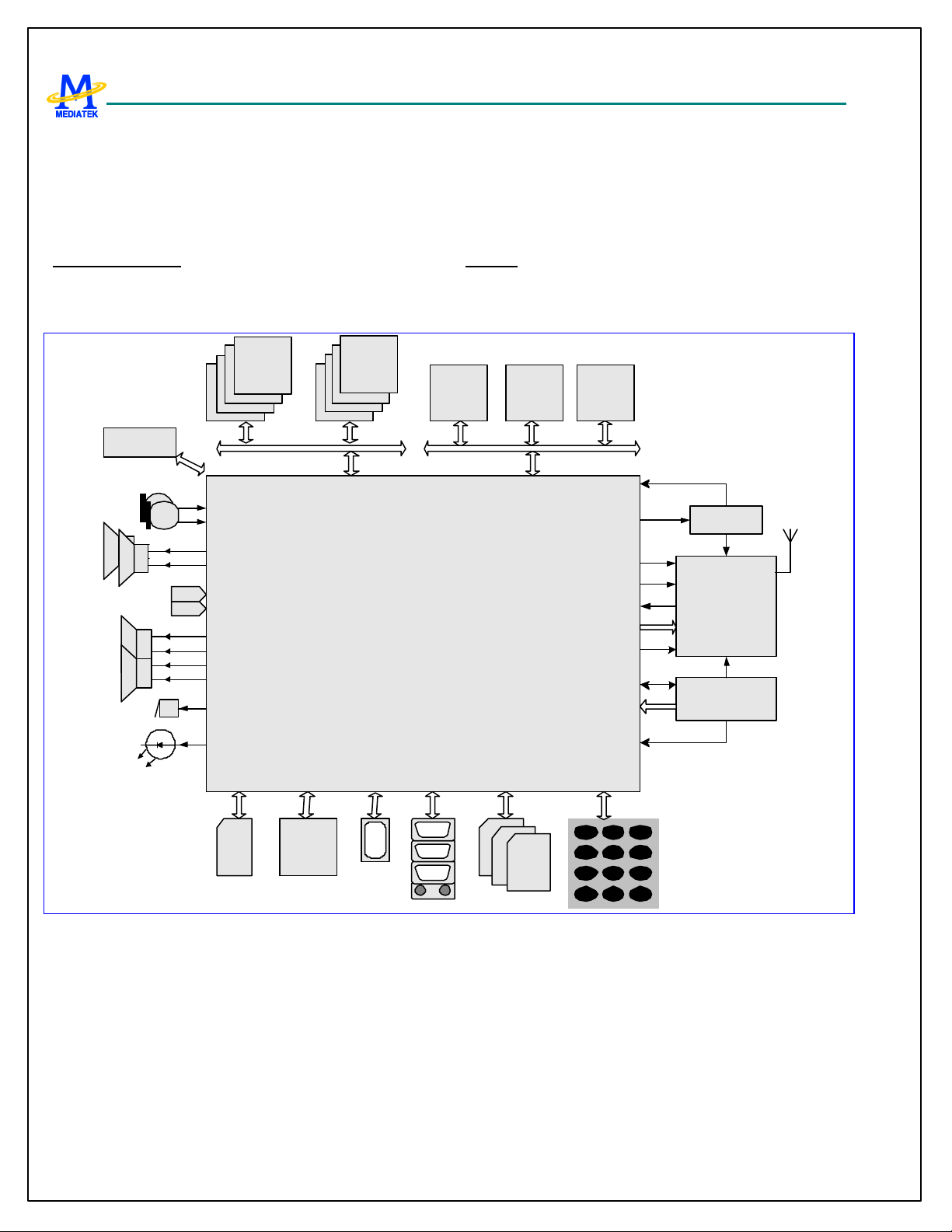
1. System Overview
The MT6217 is a highly integrated single chip solution for
GSM/GPRS phone. Based on 32-bit ARM7EJ-STM RISC
processor, MT6217 features not only high performance
GPRS Class 12 MODEM but is also designed with support
for the wireless multi-media applications, such as
advanced display engine, hardware JPEG decoder,
synthesis audio with 64-tone polyphony, digital audio
playback, Java acceleration, MMS and etc. Additionally,
MT6217 provides varieties of advanced interfaces for
functionality extensions, like 8-port external memory
inte rface, 3-port 8/16-bit parallel interface, NAND Flash,
IrDA, USB and MMC/SD/MS/MS Pro. The typical
application can be shown as Figure 1.
External Memory Interface
Providing the greatest capacity for expansion, the MT6217
supports u p to 8 state-of-the-art devices with SRAM-like
interface, including burst/page mode Flash, page mode
SRAM, Pseudo SRAM, Color/Parallel LCD, and
multi-media companion chip, like Camera and Melody
chips. Regarding the consideration of power consumption
and low noise, this interface is designed for flexible I/O
voltage and allows for lowering supply voltage down to
1.8V. In addition, the driving strength is configurable that
makes the signal integrity problem easy. Retention
technology is also specifically used on data bus to prevent
the bus from being floating during turn over.
Multi-media Subsystem
In order to provide more flexibility and bandwidth for
multi-media products, an additional 8/16 bit parallel
interface is incorporated. This interface is designed
specially for support with Camera companion chip as well
as LCD panel. Moreover, it can connect NAND flash
device to provide a solution for multi-media data storage.
For running multi-media application faster, MT6217
integrates also several hardware-based engines. With
hardware based JPEG decoder, the MT6217 easily handles
real-time playback of compressed image. With hardware
based Resizer and advanced display engine, it can display
and combine arbitrary size of images with up to 4 blending
layers.
User Interface
For user interactions, the MT6217 brings together all
necessary peripheral blocks for multi-media GSM/GPRS
phone. It comprises the Keypad Scanner with capability of
multiple key pressing, SIM Controller, Alerter, Real Time
Clock, PWM, Serial LCD Controller and General Purpose
Programmable I/Os. For connectivity and data storage, the
MT6217 consists of UART, IrDA, USB 1.1 Slave and
MMC/SD/MS/MS Pro. Besides, for large amount of data
transfer, high performance DMA (Direct Memory Access)
and hardware flow control are implemented, that greatly
enhances the performance and saves precious processing
power.
Audio Interface
With highly integrated mixed-signal Audio Front-End, the
MT6217 completes an architecture that allows for easy
audio interfacing with direct connection to the audio
transducers. Not only D/A and A/D Converters for Voice
Band, but also the high resolution Stereo D/A Converters
for Audio band are integrated. In addition, the MT6217
provides also Stereo Input and Analog Mixer. All of them
enable the MT6217 based terminal a rich platform for
multi-media applications.
Radio Interface
Providing a well-organized radio interface with flexibility
for efficient customization, the MT6217 integrates
mixed-signal Baseband Front-End. It carries out gain and
offset calibration mechanisms and filters with
programmable coefficients for comprehensive
compatibility control on RF modules. The approach is also
combining a high resolution D/A Converter for controlling
VCXO or crystal instead of TCVCXO to reduce the
overall system cost. On the other hand, with 14-bit high
resolution A/D Converter for RF downlink path, MT6217
achieves great quality of MODEM performance. Besides,
to remove the necessary of external current-driving
component, the driving strength of some BPI outputs is
designed to be configurable.
Debug Function
6/349 MediaTek Inc. Confidential
Page 7
MT6217 GSM/GPRS Baseband Processor Data Sheet Revision 1.01
The JTAG interface enables in -circuit debugging of
software program with the ARM7EJ-S core. With this
standardized debugger interface, the MT6217 provides
developers with a wide set of options for choosing ARM
development kits from supports of thirty parties.
Power Management
The MT6217 offers various low-power features helping
reduce system power consumption including Pause Mode
Flash
SRAM
PSRAM
Debugger
JTAG
Speech/Audio
Input
Speech/Audio
Output
FM Stereo
Radio Input
Melody
LCD
External Memory
Interface
MT6217
HiFi Stero
Output
Alerter
of 32KHz clocking at Standby State, Power Down Mode
for individual peripherals and Processor Sleep Mode.
Fabricated in low-power CMOS process, together with the
low-power features, the overall system can achieve ultra
low power consumption.
Package
The MT6217 device is offered in a 1 3mm×13mm, 282-ball,
0.65 mm pitch, TFBGA package.
Camera
NAND
Flash
8/16-bit Parallel
Interface
LCD
SYSCLK
AFC
APC
TX I/Q
RX I/Q
BPI
BSI
B2PSI
AuxAD
TCVCXO
RF
Module
Power
Management
C
Circuitry
PWM
SIM
Serial
LCD
Serial
LCD
USB
UART
IrDA
MMC/SD/MS/
MSPro
Supply Voltages
Keypad
1 2 3
4 5 6
7 8 9
0 #
*
Figure 1 Typical application of MT6217
7/349 MediaTek Inc. Confidential
Page 8

MT6217 GSM/GPRS Baseband Processor Data Sheet Revision 1.01
1.1 Features
n General
l Integrated voice -band, audio-band and base-band analog front ends
l TFBGA 13mm×13mm, 282-ball, 0.65 mm pitch package
n MCU Subsystem
l ARM7EJ -S 32-bit RISC processor
l Java hardware acceleration for faster Java-based games and other applets
l Operating frequency: 26/52 MHz
l 13 DMA channels
l 128 K Bytes zero -wait-state on-chip SRAM
l On-chip boot ROM for Factory Flash Programming
l Watchdog timer for system crash recovery
l 2 sets of General Purpose Timer
l Circuit Switch Data and Division coprocessors
n External Memory Interface
l Support up to 8 external devices
l Support 8-bit or 16-bit memory components with size up to 64M Bytes each
l Support Flash and SRAM with Page Mode or Burst Mode
l Support Pseudo SRAM
l Industrial standard Parallel LCD Interface
l Built-in hardware acceleration function for color LCD panels
l Support multi-media companion chips with 8/16 bits data width
l Flexible I/O voltage of 1.8V ~ 3V for memory interface
l Configurable driving strength for memory interface
n Multi-media Subsystem
l Dedicated 8/16-bit Parallel Interface, support up to 3 external devices
l High speed hardware JPEG decoder, support both baseline sequential and progressive JPEG files
l High quality hardware Resizer capable of tailoring JPEG image to arbitrary size
l Support simultaneously equipping up to 2 parallel LCD and 1 serial LCD panels
l Support LCD panel maximum resolution up to 800x600 at 16bpp
8/349 MediaTek Inc. Confidential
Page 9

MT6217 GSM/GPRS Baseband Processor Data Sheet Revision 1.01
l Capable of combining display memories with up to 4 blending layers
l NAND Flash Interface for mass storages
l Full-speed USB 1.1 Device
l Multi Media Card/Secure Digital Memory Card/Memory Stick/Memory Stick Pro controller
n Audio and Modem CODEC
l Wavetable synthesis with up to 64 notes
l Advanced wavetable synthesizer capable of generating simulated stereo
l Wavetable including GM full set of 128 instruments and 47 sets of percussion
l PCM Playback and Record
l Dial tone generation
l Voice Memo
l Noise Reduction
l Echo Suppression
l Advanced Sidetone Oscillation Reduction
l Digital sidetone generator with programmable gain
l Two programmable acoustic compensation filters
l GSM/GPRS quad vocoders for adaptive multirate (AMR), enhanced full rate (EFR), full rate (FR) and half rate (HR)
l GSM channel coding, equalization and A5/1 and A5/2 ciphering
l GPRS GEA and GEA2 ciphering
l Programmable GSM/GPRS Modem
l Packet Switched Data with CS1/CS2/CS3/CS4 coding schemes
l GSM Circuit Switch Data
l GPRS Class 12
n User Interfaces
l 6-row × 7-column keypad controller with hardware scanner
l Support multiple key press for gaming
l SIM Card Controller with hardware flow control
l 3 UARTs with hardware flow control and speed up to 921600 bps
l IrDA modulator/demodulator with hardware framer
l Real Time Clock (RTC) operating with a separate power supply
l Serial LCD Interf ace with 7 bytes TX FIFO
9/349 MediaTek Inc. Confidential
Page 10

MT6217 GSM/GPRS Baseband Processor Data Sheet Revision 1.01
l General Purpose I/Os (GPIOs)
l 2 Sets of Pulse Width Modulation (PWM) Output
l Alerter Output with Enhanced PWM or PDM
l Six external interrupt lines
n Audio Interface and Audio Front End
l Two microphone inputs sharing one low noise amplifi er with programmable gain
l Two Voice power amplifiers with programmable gain
l 2nd order Sigma -Delta A/D Converter for voice uplink path
l D/A Converter for voice downlink path
l High resolution D/A Converters for Stereo Audio playback
l Stereo analog input for ste reo audio source
l Analog Multiplexer for Stereo Audio
l Stereo to Mono Conversion
l Support half-duplex hands-free operation
l Complying with GSM 03.50
n Radio Interface and Baseband Front End
l GMSK modulator with analog I and Q channel outputs
l 10-bit D/A Converter for uplink baseband I and Q signals
l 14-bit high resolution A/D Converter for downlink baseband I and Q signals
l Calibration mechanism of offset and gain mismatch for baseband A/D Converter and D/A Converter
l 10-bit D/A Converter for Automatic Power Control
l 13-bit high resolution D/A Converter for Automatic Frequency Control
l Programmable Radio RX filter
l 2 Channels Baseband Serial Interface (BSI) with 3-wire control
l 10-Pin Baseband Parallel Interface (BPI) with programmable driving strength
l Multi-band support
n Power Management
l Power Down Mode for analog and digital circuits
l Processor Sleep Mode
l Pause Mode of 32KHz clocking at Standby State
l 7-channel Auxiliary 10-bit A/D Converter for charger and battery monitoring
10/349 MediaTek Inc. Confidential
Page 11

MT6217 GSM/GPRS Baseband Processor Data Sheet Revision 1.01
n Test and Debug
l Built-in digital and analog loop back modes for both Audio and Baseband Front-End
l DAI port complying with GSM Rec.11.10
l JTAG port for debugging embedded MCU
11/349 MediaTek Inc. Confidential
Page 12

MT6217 GSM/GPRS Baseband Processor Data Sheet Revision 1.01
1.2 General Description
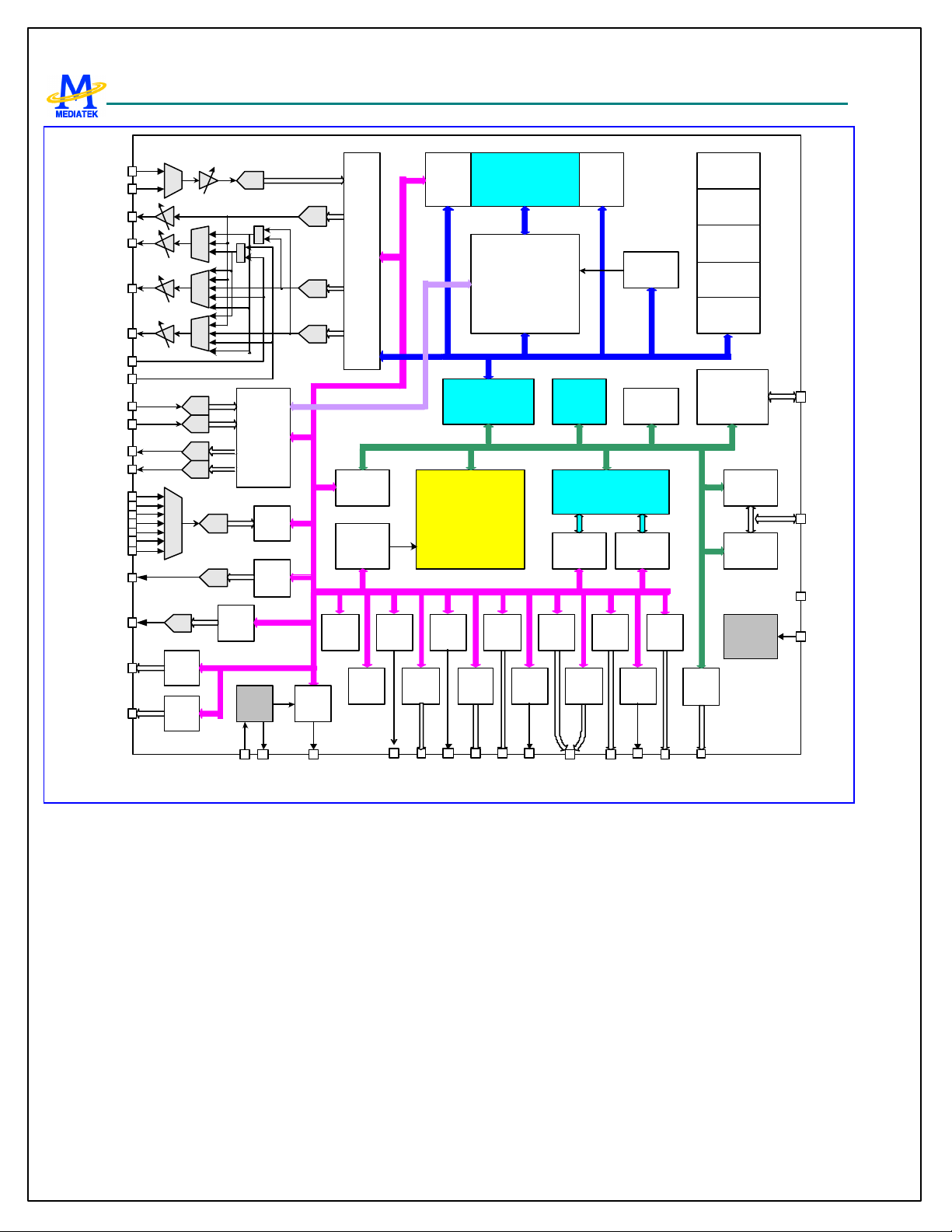
Figure 2 details the block diagram of MT6217. Based on dual-processor architecture, the major processor of MT6217 is
ARM7EJ-S, which mainly runs high-level GSM /GPRS protocol software as well as multi-media applications. With the
other one is a digital signal processor corresponding for handling the low-level MODEM as well as advanced audio
functions. Except for some mixed -signal circuitries, the other building blocks in MT6217 are connected to either the
microcontroller or the digital signal processor. Specifically, MT6217 consists of the following subsystems:
l Microcontroller Unit (MCU) Subsystem, including an ARM7EJ -S RISC processor and its accompanying memory
management and interrupt handling logics.
l Digital Signal Processor (DSP) Subsystem, including a DSP and its accompanying memory, memory controller,
and interrupt controller.
l MCU/DSP Interface, where the MCU and the DSP exchange hardware and software information.
l Microcontroller Peripherals, which includes all user interface modules and RF control interface modules.
l Microcontroller Coprocessors, which intends to run computing-intensive processes in place of Microcontroller.
l DSP Peripherals, which are hardware accelerators for GSM /GPRS channel codec.
l Multi-media Subsystem, which integrate several advanced accelerators to support multi-media applications.
l Voice Front End, the data path of conveying analog speech from and to digital speech.
l Audio Front End, also the data path of conveying stereo audio from stereo audio source
l Baseband Front End, the data path of conveying digital signal form and to analog signal of RF modules.
l Timing Generator, generating the control signals related to the TDMA frame timing.
l Power, Reset and Clock subsystem, managing the power, reset and clock distribution inside MT6217.
Details of the individual subsystems and blocks are described in following Chapters.
12/349 MediaTek Inc. Confidential
Page 13
MT6217 GSM/GPRS Baseband Processor Data Sheet Revision 1.01
MIC_0
MIC_1
VOICE_0
VOICE_1
AUDIO_L
AUDIO_R
STEREO_L
STEREO_R
RX_I
RX_Q
TX_I
TX_Q
Aux
ADC
AFC
APC
Serial RF
Control
Parallel RF
Control
MT6217
ADC
ADC
DAC
DAC
ADC
DAC AFC
DAC APC
BSI
BPI
ADC
+
+
Baseband
Path
Aux
ADC
32K
OSC
DAC
DAC
DAC
RTC
Interrupt
Controller
TDMA
Timer
Audio
Path
Bridge
GPT
WDT
SIM GPIO
Patch
Unit
ARM7EJ-S
PWM
MCU/DSP
Interface
Keypad
Scanner
Memory
DSP
Boot
ROM
Image
Resizer
Serial
LCD
B2PSI IrDA
Trap
Unit
On-Chip
SRAM
MMC
SD/MS
MS Pro
Interrupt
Controller
DMA
Controller
JPEG
Decoder
UART
DSP
Coprocessor
DSP
Coprocessor
DSP
Coprocessor
DSP
Coprocessor
DSP
Coprocessor
External
Memory
Interface
USBAlerter
LCD
Controller
NAND Flash
Controller
Clock
Generator
Flash
SRAM
LCD
Melody
NAND
Flash
LCD
Camera
JTAG
System
Clock
13/26MHz
32KHz
Crystal
Wake Up User InterfaceReset
ConnectivitySerial Port
Figure 2 MT6217 block diagram.
13/349 MediaTek Inc. Confidential
Page 14

MT6217 GSM/GPRS Baseband Processor Data Sheet Revision 1.01
2 Product Description
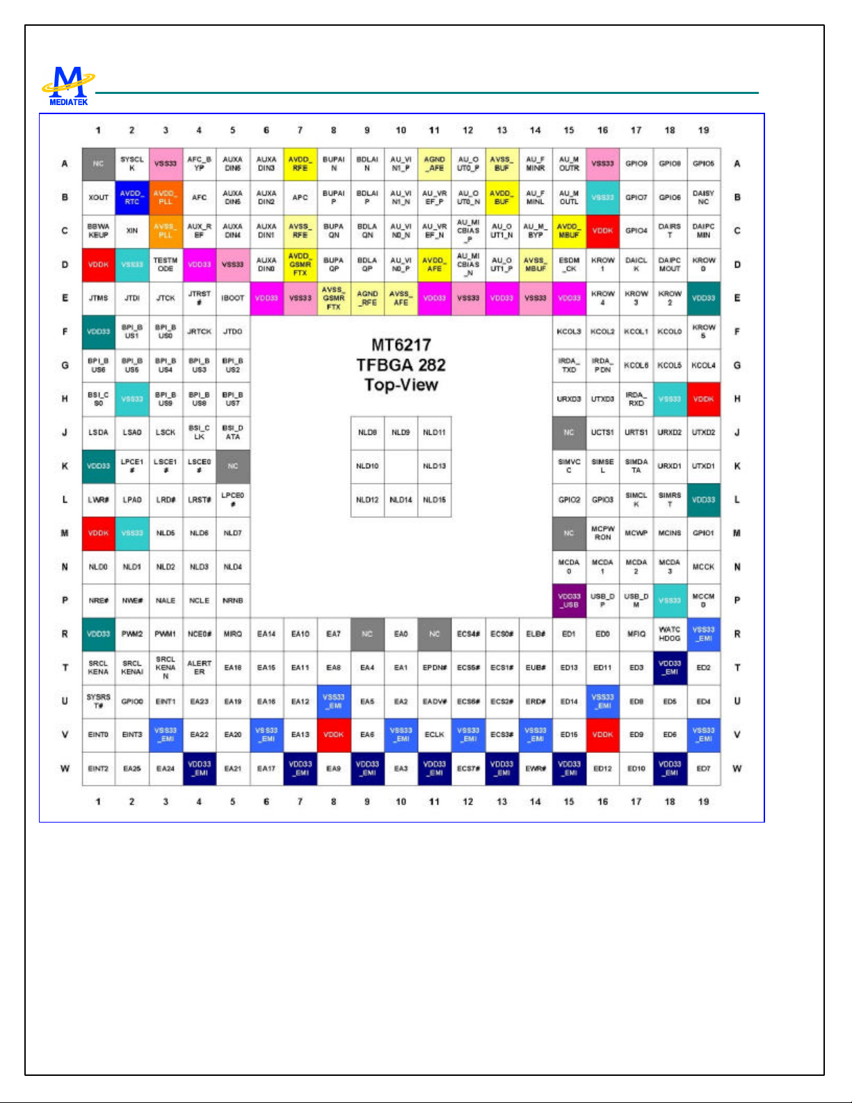
2.1 Pin Outs
One type of package for this product, TFBGA 13mm*13mm, 282-ball, 0.65 mm pitch Package, is offered.
Pin outs and the top view are illustrated in Figure 3 for this package. Outline and dimension of package is illustrated in
Figure 4, while the definition of package is shown in Table 1.
14/349 MediaTek Inc. Confidential
Page 15
MT6217 GSM/GPRS Baseband Processor Data Sheet Revision 1.01
Figure 3 Top Vi ew of MT6217 TFBGA 13mm*13mm, 282-ball, 0.65 mm pitch Package
15/349 MediaTek Inc. Confidential
Page 16

MT6217 GSM/GPRS Baseband Processor Data Sheet Revision 1.01
Figure 4 Outlines and Dimension of TFBGA 13 mm*13mm, 282-ball, 0.65 mm pitch Package
Body Size Ball Count Ball Pitch Ball Dia. Package Thk. Stand Off Substrate Thk.
D E N e b A (Max.) A1 C
13 13 282 0.65 0.3 1.4 0.3 0.36
Table 1 Definition of TFBGA 13mm*13mm, 282-ball, 0.65 mm pitch Package (Unit: mm)
16/349 MediaTek Inc. Confidential
Page 17
MT6217 GSM/GPRS Baseband Processor Data Sheet Revision 1.01
2.2 Pin Description
Ball
13 X13
Name Dir Description
JTAG Port
E4 JTRST# I
E3 JTCK I
E2 JTDI I
E1 JTMS I
F5 JTDO O
F4 JRTCK O
JTAG test port reset input
JTAG test port clock input
JTAG test port data input
JTAG test port mode switch
JTAG test port data output
JTAG test port returned clock output
RF Parallel Control Unit
F3 BPI_BUS0 O
F2 BPI_BUS1 O
G5 BPI_BUS2 O
G4 BPI_BUS3 O
G3 BPI_BUS4 O
G2 BPI_BUS5 O
G1 BPI_BUS6 IO
H5 BPI_BUS7 IO
H4 BPI_BUS8 IO
H3 BPI_BUS9 IO
RF hard-wire control bus 0
RF hard-wire control bus 1
RF hard-wire control bus 2
RF hard-wire control bus 3
RF hard-wire control bus 4
RF hard-wire control bus 5
RF hard-wire control bus 6 GPIO10 BPI_BU
RF hard-wire control bus 7 GPIO11 BPI_BU
RF hard-wire control bus 8 GPIO12 BPI_BU
RF hard-wire control bus 9 GPIO13 BPI_BU
RF Serial Control Unit
H1 BSI_CS0 O
J5 BSI_DATA O
J4 BSI_CLK O
RF 3-wire interface chip select 0
RF 3-wire interface data output
RF 3-wire interface clock output
PWM Interface
R3 PWM1 IO
R2 PWM2 IO
T4 ALERTER IO
Pulse width modulated signal 1
Pulse width modulated signal 2
Pulse width modulated signal for buzzer
Serial LCD/PM IC Interface
J3 LSCK IO
J2 LSA0 IO
J1 LSDA IO
K4 LSCE0# IO
K3 LSCE1# IO
Serial display interface data output GPIO16 LSCK TBTXE
Serial display int erface address output GPIO17 LSA0 TDTIR
Serial display interface clock output GPIO18 LSDA TCTIR
Serial display interface chip select 0
output
Serial display interface chip select 1 GPIO20 LSCE1# LPCE2# TEVTV
Mode0 Mode1 Mode2 Mode3
Pull Reset
PD Input
PU Input
PU Input
PU Input
0
0
0
0
0
0
0
0
S6
6.5MHz 26MHz
S7
13MHz 26MHz
S8
BSI_CS1
S9
PD Input
PD Input
PD Input
PD Input
0
0
0
GPIO21 PWM1 DSP_G
PO0
GPIO22 PWM2 DSP_G
PO1
GPIO23 ALERT
ER
DSP_G
PO2
TBTX
FS
TBRX
EN
BTRX
FS
PD Input
PD Input
PD Input
PU Input
N
PU Input
Q
PU Input
Q2
GPIO19 LSCE0# DSP_TI
D0
TCTIR
Q1
PU Input
PU Input
17/349 MediaTek Inc. Confidential
Page 18
MT6217 GSM/GPRS Baseband Processor Data Sheet Revision 1.01
output AL
Parallel LCD/Nand-Flash Interface
K2 LPCE1# IO
L5 LPCE0# O
L4 LRST# O
L3 LRD# O
L2 LPA0 O
L1 LWR# O
L11 NLD15 IO
L10 NLD14 IO
K11 NLD13 IO
L9 NLD12 IO
J11 NLD11 IO
K9 NLD10 IO
J10 NLD9 IO
J9 NLD8 IO
M5 NLD7 IO
M4 NLD6 IO
M3 NLD5 IO
N5 NLD4 IO
N4 NLD3 IO
N3 NLD2 IO
N2 NLD1 IO
N1 NLD0 IO
P5 NRNB IO
P4 NCLE IO
P3 NALE IO
P2 NWE# IO
P1 NRE# IO
R4 NCE0# IO
Parallel display interface chip select 1
output
Parallel display interface chip select 0
output
Parallel display interface Reset Signal
Parallel display interface Read Strobe
Parallel display interface address output
Parallel display interface Write Strobe
Parallel LCD/NAND-Flash Data 15
Parallel LCD/NAND-Flash Data 14
Parallel LCD/NAND-Flash Data 13
Parallel LCD/NAND-Flash Data 12
Parallel LCD/NAND-Flash Data 11
Parallel LCD/NAND-Flash Data 10
Parallel LCD/NAND-Flash Data 9
Parallel LCD/NAND-Flash Data 8
Parallel LCD/NAND-Flash Data 7
Parallel LCD/NAND-Flash Data 6
Parallel LCD/NAND-Flash Data 5
Parallel LCD/NAND-Flash Data 4
Parallel LCD/NAND-Flash Data 3
Parallel LCD/NAND-Flash Data 2
Parallel LCD/NAND-Flash Data 1
Parallel LCD/NAND-Flash Data 0
NAND-Flash Read/Busy Flag GPIO25
NAND-Flash Command Latch Signal GPIO26
NAND-Flash Address Latch Signal GPIO27
NAND-Flash Write Strobe GPIO28
NAND-Flash Read Strobe GPIO29
NAND-Flash Chip select output GPIO30
SIM Card Interf ace
L18 SIMRST O
L17 SIMCLK O
K15 SIMVCC O
K16 SIMSEL IO
SIM card reset output
SIM card clock output
SIM card supply power control
SIM card supply power select
GPIO24 LPCE1# NCE1# MCU_
TD0
PU
PD
PD
PD
PD
PD
PD
PD
PD
PD
PD
PD
PD
PD
PD
PD
PD
NRNB
NCLE
NALE
NWE#
NRE#
NCE0#
DSP_TI
D1
DSP_TI
D2
DSP_TI
D3
DSP_TI
D4
DSP_TI
D5
DSP_TI
D6
MCU_T
ID1
MCU_
TID2
MCU_
TID3
MCU_
DID
MCU_
DFS
MCU_
DCK
PU
PD
PD
PU
PU
PU
0
0
0
GPIO32 SIMSEL PD 0
K17 SIMDATA IO
SIM card data input/output
0
Dedicated GPIO Interface
U2 GPIO0 IO
18/349 MediaTek Inc. Confidential
General purpose input/output 0 GPIO0 DSP_GP
O3
PD Input
Page 19
MT6217 GSM/GPRS Baseband Processor Data Sheet Revision 1.01
M19 GPIO1 IO
L15 GPIO2 IO
L16 GPIO3 IO
C17 GPIO4 IO
A19 GPIO5 IO
B18 GPIO6 IO
B17 GPIO7 IO
A18 GPIO8 IO
A17 GPIO9 IO
Miscellaneous
U1 SYSRST# I
R18 WATCHD
O
OG#
T3 SRCLKEN
O
AN
T1 SRCLKENA O
T2 SRCLKEN
IO
AI
D3 TESTMODE I
General purpose input/output 1 GPIO1 DICK
General purpose input/output 2 GPIO2 DID
General purpose input/output 3 GPIO3 DIMS
General purpose input/output 4 GPIO4 DSP_CKL DSPLCK TRASD
4
General purpose input/output 5 GPIO5 AHB_C
LK
General purpose input/output 6 GPIO6 ARM_C
LK
General purpose input/output 7 GPIO7 SLOW_
CK
General purpose input/output 19 GPIO8 F32K_CK DSPLD0 TRASD
General purpose input/output 21 GPIO9 TRARS
System reset input active low
Watchdog reset output
External TCXO enable output active low
External TCXO enable output active
high
External TCXO enable input
Test Mode control input
Input
1
GPO1
GPO0
GPIO31
SRCLK
ENAN
SRCLK
ENA
SRCLK
ENAI
DSPLD3 TRASD
3
DSPLD2 TRASD
2
DSPLD1 TRASD
1
0
YNC
0
1
PD
PD
PD Input
PD Input
PD Input
PD Input
PD Input
PD Input
PD Input
PD Input
PD Input
D15 ESDM_CK O
E5 IBOOT I
Keypad Interface
G17 KCOL6 I
G18 KCOL5 I
G19 KCOL4 I
F15 KCOL3 I
F16 KCOL2 I
F17 KCOL1 I
F18 KCOL0 I
F19 KROW5 O
E16 KROW4 O
E17 KROW3 O
E18 KROW2 O
D16 KROW1 O
D19 KROW0 O
External Interrupt Interface
V1 EINT0 I
U3 EINT1 I
W1 EINT2 I
Internal monitor clock output
Boot Device Configuration Input
Keypad column 6
Keypad column 5
Keypad column 4
Keypad column 3
Keypad column 2
Keypad column 1
Keypad column 0
Keypad row 5
Keypad row 4
Keypad row 3
Keypad row 2
Keypad row 1
Keypad row 0
External interrupt 0
External interrupt 1
External interrupt 2
Input
PU Input
PU Input
PU Input
PU Input
PU Input
PU Input
PU Input
0
0
0
0
0
0
N.C.
PU Input
PU Input
PU Input
19/349 MediaTek Inc. Confidential
Page 20

MT6217 GSM/GPRS Baseband Processor Data Sheet Revision 1.01
V2 EINT3 I
R5 MIRQ IO
R17 MFIQ IO
External interrupt 3
Interrupt to MCU GPIO41 MIRQ 13MHz 6.5MHz
Interrupt to MCU GPIO42 MFIQ
External Memory Interface
R16 ED0 IO
R15 ED1 IO
T19 ED2 IO
T17 ED3 IO
U19 ED4 IO
U18 ED5 IO
V18 ED6 IO
W19 ED7 IO
U17 ED8 IO
V17 ED9 IO
W17 ED10 IO
T16 ED11 IO
W16 ED12 IO
T15 ED13 IO
U15 ED14 IO
V15 ED15 IO
U14 ERD# O
W14 EWR# O
R13 ECS0# O
T13 ECS1# O
U13 ECS2# O
V13 ECS3# O
R12 ECS4# O
T12 ECS5# O
U12 ECS6# O
W12 ECS7# IO
R14 ELB# O
T14 EUB# O
External memory data bus 0
External memory data bus 1
External memory data bus 2
External memory data bus 3
External memory data bus 4
External memory data bus 5
External memory data bus 6
External memory data bus 7
External memory data bus 8
External memory data bus 9
External memory data bus 10
External memory data bus 11
External memory data bus 12
External memory data bus 13
External memory data bus 14
External memory data bus 15
External memory read strobe
External memory write strobe
External memory chip select 0
External memory chip select 1
External memory chip select 2
External memory chip select 3
External memory chip select 4
External memory chip select 5
External memory chip select 6
External memory chip select 7
External memory lower byte strobe
External memory upper byte strobe
PU Input
PU Input
PU Input
PU/
PD
PU/
PD
PU/
PD
PU/
PD
PU/
PD
PU/
PD
PU/
PD
PU/
PD
PU/
PD
PU/
PD
PU/
PD
PU/
PD
PU/
PD
PU/
PD
PU/
PD
PU/
PD
1
1
1
1
1
1
1
1
1
GPIO40 ECS7# PU 1
1
1
Input
Input
Input
Input
Input
Input
Input
Input
Input
Input
Input
Input
Input
Input
Input
Input
20/349 MediaTek Inc. Confidential
Page 21

MT6217 GSM/GPRS Baseband Processor Data Sheet Revision 1.01
T11 EPDN# O
U11 EADV# O
V11 ECLK O
R10 EA0 O
T10 EA1 O
U10 EA2 O
W10 EA3 O
T9 EA4 O
U9 EA5 O
V9 EA6 O
R8 EA7 O
T8 EA8 O
W8 EA9 O
R7 EA10 O
T7 EA11 O
U7 EA12 O
V7 EA13 O
R6 EA14 O
T6 EA15 O
U6 EA16 O
W6 EA17 O
T5 EA18 O
U5 EA19 O
V5 EA20 O
W5 EA21 O
V4 EA22 O
U4 EA23 O
W3 EA24 O
W2 EA25 O
USB Interface
P16 USB_DP IO
P17 USB_DM IO
Memory Card Interface
P19 MCCM0 IO
N15 MCDA0 IO
N16 MCDA1 IO
N17 MCDA2 IO
N18 MCDA3 IO
N19 MCCK O
M16 MCPWRO O
Power Down Control Signal for PSRAM
Address valid for burst mode flash
memory
Clock for flash memory
External memory ad dress bus 0
External memory address bus 1
External memory address bus 2
External memory address bus 3
External memory address bus 4
External memory address bus 5
External memory address bus 6
External memory address bus 7
External memory address bus 8
External memory address bus 9
External memory address bus 10
External memory address bus 11
External memory address bus 12
External memory address bus 13
External memory address bus 14
External memory address bus 15
External memory ad dress bus 16
External memory address bus 17
External memory address bus 18
External memory address bus 19
External memory address bus 20
External memory address bus 21
External memory address bus 22
External memory address bus 23
External memory address bus 24
External memory address bus 25
USB D+ Input/Output
USB D- Input/Output
SD Command/MS Bus State Output
SD Serial Data IO 0/MS Serial Data IO
SD Serial Data IO 1
SD Serial Data IO 2
SD Serial Data IO 3
SD Serial Clock/MS Serial Clock Output
SD Power On Control Output
GPO2 EPDN# 0
1
0
0
0
0
0
0
0
0
0
0
0
0
0
0
0
0
0
0
0
0
0
0
0
0
0
0
0
PU/
PD
PU/
PD
PU/
PD
PU/
PD
PU/
PD
21/349 MediaTek Inc. Confidential
Page 22
MT6217 GSM/GPRS Baseband Processor Data Sheet Revision 1.01
N
M17 MCWP I
M18 MCINS I
UART Interface
K18 URXD1 I
K19 UTXD1 O
J16 UCTS1 I
J17 URTS1 O
J18 URXD2 IO
J19 UTXD2 IO
H15 URXD3 IO
H16 UTXD3 IO
H17 IRDA_RXD IO
G15 IRDA_TXD IO
G16 IRDA_PDN IO
Digital Audio Interface
D17 DAICLK IO
D18 DAIPCM O
IO
UT
C19 DAIPCMIN IO
C18 DAIRST IO
B19 DAISYNC IO
SD Write Protect Input GPIO15 MCWP
SD Card Detect Inp ut GPIO14 MCINS
UART 1 receive data PU Input
UART 1 transmit data 1
UART 1 clear to send PU Input
UART 1 request to send 1
UART 2 receive data GPIO35 URXD2 UCTS3 PU Input
UART 2 transmit data GPIO36 UTXD2 URTS3 PU Input
UART 3 receive data GPIO33 URXD3 PU Input
UART 3 transmit data GPIO34 UTXD3 PU Input
IrDA receive data GPIO37 IRDA_R
XD
IrDA transmit data GPIO38 IRDA_T
XD
IrDA Power Down Control GPIO39 IRDA_P
DN
DAI clock output GPIO43 DAICLK TDMA_
DAI pcm data out GPIO44 DAIPC
MOUT
DAI pcm data input GPIO45 DAIPC
MIN
DAI reset signal input GPIO47 DAIRST TDMA_
DAI frame synchronizat ion signal output GPIO46 DAISYNC BFEPRBO TRASD5 PU Input
UCTS2 PU Input
URTS2 PU Input
PU Input
TRACLK PU Input
CK
TDMA_
D1
TDMA_
D2
FS
TRASY
NC
TRASD7 PU Input
TRASD6 PU Input
PU
PU
PD Input
Analog Interface
B15 AU_MOUL
A15 AU_MOUR
C14 AU_M_BYP
B14 AU_FMINL
A14 AU_FMINR
D13 AU_OUT1_P
C13 AU_OUT1_N
B12 AU_OUT0_N
A12 AU_OUT0_P
C12 AU_MICBI
Audio analog output left channel
Audio analog output right channel
Audio DAC bypass pin
FM radio analog input left channel
FM radio analog input right channel
Earphone 1 amplifier output (+)
Earphone 1 amplifier output (-)
Earphone 0 amplifier output (-)
Earphone 0 amplifier output (+)
Microphone bias supply (+)
AS_P
D12 AU_MICBI
22/349 MediaTek Inc. Confidential
Microphone bias supply (-)
Page 23

MT6217 GSM/GPRS Baseband Processor Data Sheet Revision 1.01
AS_N
C11 AU_VREF_N
Audio reference voltage (-)
B11 AU_VREF_P
D10 AU_VIN0_P
C10 AU_VIN0_N
B10 AU_VIN1_N
A10 AU_VIN1_P
D9 BDLAQP
C9 BDLAQN
A9 BDLAIN
B9 BDLAIP
B8 BUPAIP
A8 BUPAIN
C8 BUPAQN
D8 BUPAQP
B7 APC
D6 AUXADIN
Audio reference voltage (+)
Microphone 0 amplifier input (+)
Microphone 0 amplifier input (-)
Microphone 1 amplifier input (-)
Microphone 1 amplifier input (+)
Quadrature input (Q+) baseband code c
downlink
Quadrature input (Q-) baseband codec
downlink
In-phase input (I+) baseband codec
downlink
In-phase input (I-) baseband codec
downlink
In-phase output (I+) baseband codec
uplink
In-phase output (I-) baseband codec
uplink
Quadrature output (Q+) baseband codec
uplink
Quadrature output (Q -) baseband codec
uplink
Automatic power control DAC output
Auxiliary ADC input 0
0
C6 AUXADIN
Auxiliary ADC input 1
1
B6 AUXADIN
Auxiliary ADC input 2
2
A6 AUXADIN
Auxiliary ADC input 3
3
C5 AUXADIN
Auxiliary ADC input 4
4
B5 AUXADIN
Auxiliary ADC input 5
5
A5 AUXADIN
Auxiliary ADC input 6
6
C4 AUX_REF
B4 AFC
A4 AFC_BYP
Auxiliary ADC reference voltage input
Automatic frequency control DAC
output
Automatic frequency control DAC
bypass capacitance
VCXO Interface
A2 SYSCLK
13MHz or 26MHz system clock input
23/349 MediaTek Inc. Confidential
Page 24

MT6217 GSM/GPRS Baseband Processor Data Sheet Revision 1.01
RTC Interface
C2 XIN
B1 XOUT
C1 BBWAKEUP O
Supply Voltages
D1 VDDK
M1 VDDK
V8 VDDK
V16 VDDK
H19 VDDK
C16 VDDK
W4 VDD33_E
MI
W7 VDD33_E
MI
W9 VDD33_E
MI
W11 VDD33_E
MI
W13 VDD33_E
MI
W15 VDD33_E
MI
W18 VDD33_E
MI
T18 VDD33_E
MI
V3 VSS33_EMI
32.768 KHz crystal input
32.768 KHz crystal output
Baseband power on/off control
Supply voltage of internal logic
Supply voltage of internal logic
Supply voltage of internal logic
Supply voltage of internal logic
Supply voltage of internal logic
Supply voltage of internal logic
Supply voltage of memory interface
driver
Supply voltage of memory interface
driver
Supply voltage of memory interface
driver
Supply voltage of memory interface
driver
Supply voltage of memory interface
driver
Supply voltage of memory interface
driver
Supply voltage of memory interface
driver
Supply voltage of memory interface
driver
Ground of memory interface driver
1
V6 VSS33_EMI
U8 VSS33_EMI
V10 VSS33_EMI
V12 VSS33_EMI
V14 VSS33_EMI
U16 VSS33_EMI
V19 VSS33_EMI
R19 VSS33_EMI
P15 VDD33_US
Ground of memory interface driver
Ground of memory interface driver
Ground of memory interface driver
Ground of memory interface driver
Ground of memory interface driver
Ground of memory interface driver
Ground of memory interface driver
Ground of memory interface driver
Supply voltage of drivers for USB
B
24/349 MediaTek Inc. Confidential
Page 25

MT6217 GSM/GPRS Baseband Processor Data Sheet Revision 1.01
D4 VDD33
F1 VDD33
K1 VDD33
R1 VDD33
L19 VDD33
E19 VDD33
E15 VDD33
E13 VDD33
E11 VDD33
E6 VDD33
A3 VSS33
D2 VSS33
D5 VSS33
H2 VSS33
M2 VSS33
P18 VSS33
H18 VSS33
A16 VSS33
B16 VSS33
E14 VSS33
E12 VSS33
E7 VSS33
B3 AVDD_PLL
Supply voltage of drivers except
memory interface and USB
Supply voltage of drivers except
memory interface and USB
Supply voltage of drivers except
memory interface and USB
Supply voltage of drivers except
memory interface and USB
Supply voltage of drivers except
memory interface and USB
Supply voltage of drivers except
memory interface and USB
Supply voltage of drivers except
memory interface and USB
Supply voltage of drivers except
memory interface and USB
Supply voltage of drivers except
memory interface and USB
Supply voltage of drivers except
memory interface and USB
Ground of drivers except memory
interface
Ground of drivers except memory
interface
Ground of drivers except memory
interface
Ground of drivers except memory
interface
Ground of drivers except memory
interface
Ground of drivers except memory
interface
Ground of drivers except memory
interface
Ground of drivers except memory
interface
Ground of drivers except memory
interface
Ground of drivers except memory
interface
Ground of drivers except memory
interface
Ground of drivers except memory
interface
Supply voltage for PLL
C3 AVSS_PLL
B2 AVDD_RTC
Ground for PLL supply
Supply voltage for Real Time Clock
Analog Supplies
C15 AVDD_MB
Supply Voltage for Audio band section
UF
25/349 MediaTek Inc. Confidential
Page 26
MT6217 GSM/GPRS Baseband Processor Data Sheet Revision 1.01
D14 AVSS_MB
UF
B13 AVDD_BUF
A13 AVSS_BUF
D11 AVDD_AFE
A11 AGND_AFE
E10 AVSS_AFE
E9 AGND_RFE
E8 AVSS_GS
MRFTX
D7 AVDD_GS
MRFTX
C7 AVSS_RFE
A7 AVDD_RFE
GND for Audio band section
Supply voltage for voice band transmit
section
GND for voice band transmit section
Supply voltage for voice band receive
section
GND reference voltage for voice band
section
GND for voice band receive section
GND reference voltage for baseband
section, APC, AFC and AUXADC
GND for baseband transmit section
Supply voltage for baseband transmit
section
GND for baseband receive section, APC,
AFC and AUXADC
Supply voltage for baseband receive
section, APC, AFC and AUXADC
Table 2 Pin Descriptions (Bolded types are functions at reset)
26/349 MediaTek Inc. Confidential
Page 27

MT6217 GSM/GPRS Baseband Processor Data Sheet Revision 1.01
2.3 Power Description
Ball
13X13
B17 GPIO7 VDDK VSSK
A18 GPIO8 VDDK VSSK
A17 GPIO9
B16 VSS33
A16 VSS33
C16 VDDK Typ. 1.8V
E15 VDD33 Typ. 2.8V
D15 ESDM_CK VDD33 VSS33 VDDK VSSK
E14 VSS33
E13 VDD33 Typ. 2.8V
E12 VSS33
E11 VDD33 Typ. 2.8V
E7 VSS33
J9 NLD8
J10 NLD9
K9 NLD10
J11 NLD11
E6 VDD33 Typ. 2.8V
L9 NLD12
K11 NLD13
Name IO Suppl y IO GND Core Supply Core GND Remark
VDD33 VSS33
VDDK VSSK
VDD33 VSS33 VDDK VSSK
VDD33 VSS33 VDDK VSSK
L10 NLD14
L11 NLD15
D5 VSS33
D4 VDD33 Typ. 2.8V
A3 VSS33
B3 AVDD_PLL Typ. 2.8V
A2 SYSCLK AVDD_PLL AVSS_PLL AVDD_PLL AVSS_PLL
C3 AVSS_PLL
B2 AVDD_RTC Typ. 1.5V
B1 XOUT AVDD_RTC VSS33 AVDD_RTC VSS33
C2 XIN AVDD_RTC VSS33 AVDD_RTC VSS33
C1 BBWAKEUP AVDD_RTC VSS33 AVDD_RTC VSS33
D2 VSS33
D3 TESTMODE VDD33 VSS33 VDDK VSSK
D1 VDDK Typ. 1.8V
27/349 MediaTek Inc. Confidential
Page 28

MT6217 GSM/GPRS Baseband Processor Data Sheet Revision 1.01
E5 IBOOT VDDK VSSK
VDD33 VSS33
E4 JTRST# VDDK VSSK
E3 JTCK VDDK VSSK
E2 JTDI VDDK VSSK
E1 JTMS VDDK VSSK
F5 JTDO VDDK VSSK
F4 JRTCK VDDK VSSK
F3 BPI_BUS0 VDDK VSSK
F2 BPI_BUS1
VDDK VSSK
F1 VDD33 Typ. 2.8V
G5 BPI_BUS2 VDDK VSSK
VDD33 VSS33
G4 BPI_BUS3 VDDK VSSK
G3 BPI_BUS4 VDDK VSSK
G2 BPI_BUS5 VDDK VSSK
G1 BPI_BUS6 VDDK VSSK
H5 BPI_BUS7 VDDK VSSK
H4 BPI_BUS8
VDDK VSSK
H2 VSS33
H3 BPI_BUS9 VDDK VSSK
VDD33 VSS33
H1 BSI_CS0 VDDK VSSK
J5 BSI_DATA VDDK VSSK
J4 BSI_CLK VDDK VSSK
J3 LSCK VDDK VSSK
J2 LSA0 VDDK VSSK
J1 LSDA VDDK VSSK
K4 LSCE0# VDDK VSSK
K3 LSCE1#
VDDK VSSK
K1 VDD33
K2 LPCE1# VDDK VSSK
VDD33 VSS33
L5 LPCE0# VDDK VSSK
L4 LRST# VDDK VSSK
L3 LRD# VDDK VSSK
L2 LPA0 VDDK VSSK
L1 LWR# VDDK VSSK
M5 NLD7 VDDK VSSK
M4 NLD6 VDDK VSSK
M3 NLD5
VDDK VSSK
M2 VSS33
M1 VDDK Typ. 1.8V
28/349 MediaTek Inc. Confidential
Page 29
MT6217 GSM/GPRS Baseband Processor Data Sheet Revision 1.01
N5 NLD4 VDDK VSSK
VDD33 VSS33
N4 NLD3 VDDK VSSK
N3 NLD2 VDDK VSSK
N2 NLD1 VDDK VSSK
N1 NLD0 VDDK VSSK
P5 NRNB VDDK VSSK
P4 NCLE VDDK VSSK
P3 NALE VDDK VSSK
P2 NEW# VDDK VSSK
P1 NRE# VDDK VSSK
R4 NCE#
VDDK VSSK
R1 VDD33 Typ. 2.8V
R3 PWM1 VDDK VSSK
VDD33 VSS33
R2 PWM2 VDDK VSSK
T4 ALERTER VDDK VSSK
T1 SRCLKENA VDDK VSSK
T3 SRCLKENAN VDDK VSSK
T2 SRCLKENAI VDDK VSSK
U1 SYSRST# VDDK VSSK
U2 GPIO0 VDDK VSSK
V1 EINT0 VDDK VSSK
U3 EINT1 VDDK VSSK
W1 EINT2 VDDK VSSK
V2 EINT3
VDDK VSSK
V3 VSS33_EMI
W2 EA25 VDDK VSSK
W3 EA24 VDDK VSSK
VDD33_EMI VSS33_EMI
U4 EA23 VDDK VSSK
V4 EA22
VDDK VSSK
W4 VDD33_EMI Typ. 1.8~2.8V
R5 MIRQ VDDK VSSK
W5 EA21 VDDK VSSK
VDD33_EMI VSS33_EMI
V5 EA20 VDDK VSSK
U5 EA19 VDDK VSSK
T6 EA18
VDDK VSSK
V6 VSS33_EMI
W6 EA17 VDDK VSSK
U6 EA16 VDDK VSSK
T6 EA15
VDD33_EMI VSS33_EMI
VDDK VSSK
29/349 MediaTek Inc. Confidential
Page 30

MT6217 GSM/GPRS Baseband Processor Data Sheet Revision 1.01
R6 EA14 VDDK VSSK
W7 VDD33_EMI Typ. 1.8~2.8V
V7 EA13 VDDK VSSK
VDD33_EMI VSS33_EMI
U7 EA12 VDDK VSSK
T7 EA11 VDDK VSSK
R7 EA10
VDDK VSSK
V8 VDDK Typ. 1.8V
U8 VSS33_EMI
W8 EA9 VDDK VSSK
T8 EA8 VDDK VSSK
VDD33_EMI VSS33_EMI
R8 EA7 VDDK VSSK
V9 EA6
VDDK VSSK
W9 VDD33_EMI Typ. 1.8~2.8V
U9 EA5 VDDK VSSK
T9 EA4 VDDK VSSK
W10 EA3
VDD33_EMI VSS33_EMI
VDDK VSSK
V10 VSS33_EMI
U10 EA2 VDDK VSSK
VDD33_EMI VSS33_EMI
T10 EA1 VDDK VSSK
R10 EA0
VDDK VSSK
W11 VDD33_EMI Typ. 1.8~2.8V
U11 EADV# VDDK VSSK
VDD33_EMI VSS33_EMI
V11 ECLK VDDK VSSK
T11 EPDN#
VDDK VSSK
V12 VSS33_EMI
W12 ECS7# VDDK VSSK
VDD33_EMI VSS33_EMI
U12 ECS6# VDDK VSSK
T12 ECS5# VDDK VSSK
R12 ECS4#
VDDK VSSK
W13 VDD33_EMI Typ. 1.8~2.8V
V13 ECS3# VDDK VSSK
U13 ECS2# VDDK VSSK
VDD33_EMI VSS33_EMI
T13 ECS1# VDDK VSSK
R13 ECS0#
VDDK VSSK
V14 VSS33_EMI
W14 EWR# VDDK VSSK
U14 ERD# VDDK VSSK
VDD33_EMI VSS33_EMI
T14 EUB# VDDK VSSK
R14 ELB#
30/349 MediaTek Inc. Confidential
VDDK VSSK
Page 31

MT6217 GSM/GPRS Baseband Processor Data Sheet Revision 1.01
W15 VDD33_EMI Typ. 1.8~2.8V
V15 ED15 VDDK VSSK
VDD33_EMI VSS33_EMI
U15 ED14 VDDK VSSK
T15 ED13 VDDK VSSK
W16 ED12
VDDK VSSK
V16 VDDK
U16 VSS33_EMI
T16 ED11 VDDK VSSK
VDD33_EMI VSS33_EMI
W17 ED10 VDDK VSSK
V17 ED9
VDDK VSSK
W18 VDD33_EMI Typ. 1.8~2.8V
U17 ED8 VDDK VSSK
VDD33_EMI VSS33_EMI
W19 ED7 VDDK VSSK
V18 ED6
VDDK VSSK
V19 VSS33_EMI
U18 ED5 VDDK VSSK
VDD33_EMI VSS33_EMI
U19 ED4 VDDK VSSK
T17 ED3
VDDK VSSK
T18 VDD33_EMI Typ. 1.8~2.8V
T19 ED2 VDDK VSSK
R15 ED1 VDDK VSSK
VDD33_EMI VSS33_EMI
R16 ED0 VDDK VSSK
R17 MFIQ VDDK VSSK
R18 WATCHDOG
VDDK VSSK
R19 VSS33_EMI
P15 VDD33_USB Typ. 3.3V
P16 USB_DP VDDK VSSK
P17 USB_DM
VDD33_USB VSS33_USB
VDDK VSSK
P18 VSS33
P19 MCCM0 VDDK VSSK
N15 MCDA0 VDDK VSSK
VDD33
VSS33
N16 MCDA1 VDDK VSSK
N17 MCDA2 VDDK VSSK
N18 MCDA3 VDDK VSSK
N19 MCCK VDDK VSSK
M16 MCPWRON VDDK VSSK
M17 MCWP VDDK VSSK
M18 MCINS VDDK VSSK
M19 GPIO1
31/349 MediaTek Inc. Confidential
VDDK VSSK
Page 32

MT6217 GSM/GPRS Baseband Processor Data Sheet Revision 1.01
L15 GPIO2 VDDK VSSK
L16 GPIO3 VDDK VSSK
L19 VDD33 Typ. 2.8V
L18 SIMRST VDDK VSSK
L17 SIMCLK VDDK VSSK
VDD33
VSS33
K15 SIMVCC VDDK VSSK
K16 SIMSEL VDDK VSSK
K17 SIMDATA VDDK VSSK
K18 URXD1 VDDK VSSK
K19 UTXD1 VDDK VSSK
J16 UCTS1 VDDK VSSK
J17 URTS1 VDDK VSSK
J18 URXD2 VDDK VSSK
J19 UTXD2 VDDK VSSK
H15 URXD3 VDDK VSSK
H16 UTXD3
VDDK VSSK
H19 VDDK VDDK VSSK Typ. 1.8V
H18 VSS33 VDDK VSSK
H17 IRDA_PDN VDDK VSSK
G15 IRDA_TXD VDDK VSSK
VDD33
VSS33
G16 IRDA_RXD VDDK VSSK
G17 KCOL6 VDDK VSSK
G18 KCOL5 VDDK VSSK
G19 KCOL4 VDDK VSSK
F15 KCOL3 VDDK VSSK
F16 KCOL2 VDDK VSSK
F17 KCOL1 VDDK VSSK
F18 KCOL0 VDDK VSSK
F19 KROW5 VDDK VSSK
E16 KROW4 VDDK VSSK
E17 KROW3 VDDK VSSK
E18 KROW2
VDDK VSSK
E19 VDD33 Typ. 2.8V
D16 KROW1 VDDK VSSK
VDD33 VSS33
D19 KROW0 VDDK VSSK
D17 DAICLK VDDK VSSK
D18 DAIPCMOUT VDDK VSSK
C19 DAIPCMIN VDDK VSSK
C18 DAIRST
VDDK VSSK
32/349 MediaTek Inc. Confidential
Page 33

MT6217 GSM/GPRS Baseband Processor Data Sheet Revision 1.01
B19 DAISYNC VDDK VSSK
C17 GPIO4 VDDK VSSK
A19 GPIO5 VDDK VSSK
A18 GPIO6 VDDK VSSK
C15 AVDD_MBUF Typ. 2.8V
B15 AU_MOUTL
A15 AU_MOUTR
D14 AVSS_MBUF
C14 AU_M_BYP
B14 AU_FMINL
A14 AU_FMINR
D13 AU_OUT1_P
C13 AU_OUT1_N
B12 AU_OUT0_N
B13 AVDD_BUF Typ. 2.8V
A12 AU_OUT0_P
A13 AVSS_BUF
C12 AU_MICBIAS_P
D12 AU_MICBIAS_N
D11 AVDD_AFE Typ. 2.8V
C11 AU_VREF_N
B11 AU_ VREF_P
A11 AGND_AFE
D10 AU_VIN0_P
C10 AU_VIN0_N
B10 AU_VIN1_N
A10 AU_VIN1_P
E10 AVSS_AFE
D9 BDLAQP
C9 BDLAQN
E9 AGND_RFE
A9 BDLAIN
B9 BDLAIP
E8 AVSS_GSMRFTX
B8 BUPAIP
A8 BUPAIN
D7 AVDD_GSMRFTX Typ. 2.8V
C8 BUPAQN
D8 BUPAQP
33/349 MediaTek Inc. Confidential
Page 34

MT6217 GSM/GPRS Baseband Processor Data Sheet Revision 1.01
C7 AVSS_RFE
B7 APC
A7 AVDD_RFE Typ. 2.8V
D6 AUXADIN0
C6 AUXADIN1
B6 AUXADIN2
A6 AUXADIN3
C5 AUXADIN4
B5 AUXADIN5
A5 AUXADIN6
C4 AUX_REF
B4 AFC
A4 AFC_BYP
Table 3 Power Descriptions
34/349 MediaTek Inc. Confidential
Page 35

MT6217 GSM/GPRS Baseband Processor Data Sheet Revision 1.01
3 Micro-Controller Unit Subsystem
Figure 5 illustrates the block diagram of the Micro-Controller Unit Subsystem in MT6217. A 32-bit RISC processor,
ARM7EJ-S, plays the role of the major bus master controlling the whole subsystem. Essentially, it communicates with all
the other on-chip modules by way of system buses: AHB Bus and APB Bus.
All bus transactions originate from bus masters, while slaves can only respond requests from bus masters. Prior to a data
transfer can be established, bus master must ask for bus ownership. This is accomplished by request-grant handshaking
protocol between masters and arbiters.
Two levels of bus hierarchy are designed to provide alternatives for different performance requirements, i.e. AHB Bus and
APB Bus for system back bone and peripheral buses, respectively. To have high performance and proper efficiency, the
AHB Bus provides 32 -bit data path with multiplex scheme for bus interconnections.
For APB Bus, it supports 16-bit addressing and both 16 -bit and 32-bit data paths. Since it is designated to reduce interface
complexity for lower data transfer rate, it is isolated from high bandwidth AHB Bus by APB Bridge. APB Bus is also
optimized for minimal power consumption by employing gated -clock scheme.
Whenever the target slave locates on AHB Bus, the transaction is conducted directly on AHB Bus. However, if the target
slave is a peripheral, the transaction should be further forwarded to APB Bus by APB Bridge.
Only memory addressing method is used in MT 6217 based system. All components are mapped onto MCU 32 -bit address
space. A Memory Management Unit is employed to have a central decode scheme. It generates certain selection signals for
each memory -addressed modules on AHB Bus.
In order to off-load the processor core, a DMA Controller is designated to act as a master and share the bus resources on
AHB Bus to do fast data movement between modules. This controller comprises thirteen DMA channels.
The Interrupt Controller provides a software interface to manipulate interrupt events. It can handle up to 32 interrupt
sources asserted at the same time. In general, it generates 2 levels of interrupt requests, FIQ and IRQ, to the processor.
A 256K Byte SRAM is provided for acting as system memory for high -speed data access. For factory programming
purpose, a Boot ROM module is used. These two modules use the same Internal Memory Controller to connect to AHB
Bus.
External Memory Interface supports both 8-bit and 16-bit devices. Since AHB Bus is 32-bit wide, all the data transfer will
be converted into several 8-bit or 16 -bit cycles depending on the data width of target device. Note that, this interface is
specific to both synchronous and asynchronous components, like Flash, SRAM and parallel LCD. This interface supports
also page and burst mode type of Flash.
35/349 MediaTek Inc. Confidential
Page 36

MT6217 GSM/GPRS Baseband Processor Data Sheet Revision 1.01
System ROM
System RAM
Internal Memory
Controller
Ext
Bus
Figure 5 Block Diagram of the Micro -Controller Unit Subsystem in MT 6217
External
Memory
Interface
MCU-DSP
Interface
Arbiter
AHB Bus
USB
ARM7EJ-S
DMA
Controller
Peripheral
Interrupt
Controller
APB
Bridge
APB Bus
Peripheral
3.1 Processor Core
3.1.1 General Description
The Micro-Controller Unit Subsystem in MT 6217 is built up with a 32-bit RISC core, ARM7EJ-S that is based on Von
Neumann architecture with a single 32 -bit data bus carrying both instructions and data. The memory interface of
ARM7EJ-S is totally compliant to AMBA based bus system. Basically, it can be connected to AHB Bus directly.
3.2 Memory Management
3.2.1 General Description
The processor core of MT 6217, ARM7EJ -S, supports only memory addressing method for instruction fetch and data access.
It manages a 32 -bit address space that has addressing capability up to 4GB. System RAM, System ROM, Registers, MCU
Peripherals and external components are all mapped onto such 32 -bit address space, as depicted in Figure 6.
36/349 MediaTek Inc. Confidential
Page 37

MT6217 GSM/GPRS Baseband Processor Data Sheet Revision 1.01
MCU 32-bit
Addressing
Space
9FFF_FFFh
|
9000_0000h
8FFF_FFFFh
|
8000_0000h
7FFF_FFFFh
|
7000_0000h
6FFF_FFFFh
|
5000_0000h
4FFF_FFFFh
|
4000_0000h
9800_0000h
9000_0000h LCD
7800_0000h
7000_0000h USB
Reserved
Reserved
APB Peripherals
Virtual FIFO
MCU-DSP Interface
Internal Memory
3FFF_FFFFh
|
0000_0000h
External Memroy
EA[25:0]
Addressing
Space
Figure 6 The Memory Layout of MT6217
The address space is organized as basis of blocks with size of 256M Bytes for each. Memory blocks MB0-MB9 are
determined and currently dedicated to specific functions, as shown in Table 4 , while the others are reserved for future usage.
Essentially, the block number is uniquely selected by address line A31-A28 of internal system bus.
Memory
Block
MB0 0h
Block Address
A31-A28
Address Range Description
00000000h-07FFFFFFh Boot Code, EXT SRAM or EXT Flash/MISC
08000000h-0FFFFFFFh EXT SRAM or EXT Flash/MISC
MB1 1h
10000000h-17FFFFFFh EXT SRAM or EXT Flash/MISC
18000000h-1FFFFFFFh EXT SRAM or EXT Flash/MISC
MB2 2h
20000000h-27FFFFFFh EXT SRAM or EXT Flash/MISC
28000000h-2FFFFFFFh EXT SRAM or EXT Flash/MISC
MB3 3h
30000000h-37FFFFFFh EXT SRAM or EXT Flash/MISC
38000000h-3FFFFFFFh EXT SRAM or EXT Flash/MISC
37/349 MediaTek Inc. Confidential
Page 38

MT6217 GSM/GPRS Baseband Processor Data Sheet Revision 1.01
MB4 4h
MB5 5h 50000000h-5FFFFFFFh
MB6 6h 60000000h-6FFFFFFFh
MB7 7h
MB8 8h 80000000h-8FFFFFFFh APB Slaves
MB9 9h
40000000h-47FFFFFFh System RAM
48000000h-4FFFFFFFh System ROM
MCU-DSP Interface
70000000h-77FFFFFFh USB
78000000h-7FFFFFFFh Virtual FIFO
90000000h-97FFFFFFh LCD
Table 4 Definitions of Memory Blocks in MT 6217
3.2.1.1 External Access
To have external access, the MT 6217 outputs 26 bits (A25-A0) of address lines along with 8 selection signals that
correspond to associated memory blocks. That is, MT 6217 can support at most 8 MCU addressable external components.
The data width of internal system bus is fixed as 32-bit wide, while the data width of the external components can be either
8 or 16 bit.
Since devices are usually available with variety operating grades, adaptive configurations for different applications are
needed. MT6217 provides software programmable registers to configure to adapt operating conditions in terms of different
wait-states.
3.2.1.2 Memory Re-mapping Mechanism
To permit system being configured with more flexible, a memory re -mapping mechanism is provided. It allows software
program to swap BANK0 (ECS0#) and BANK1 (ECS1#) dynamically. Whenever the bit value of RM0 in register
EMI_REMAP is changed, these two banks will be swapped accordingly. Besides, it also permits system being boot in
different sequence as detailed in 3.2.1.3 Boot Sequence.
3.2.1.3 Boot Sequence
Since the ARM7EJ-S core always starts to fetch instructions from the lowest memory address at 00000000h (MB0) after
system being reset. It is designed to have a dynamic mapping architecture capable of associating Boot Code, external Flash
or external SRAM with memory block MB0.
By default, the Boot Code is mapped onto MB0 while the state of IBOOT is “0”. But, this configuration can be changed by
altering the state of IBOOT before system reset or programming bit value of RM1 in register EMI_REMAP directly.
MT 6217 system provides two kinds of boot up scheme:
l Start up system of running codes from Boot Code for factory programming
l Start up system of running codes from external FLASH or ROM device for normal operation
38/349 MediaTek Inc. Confidential
Page 39

MT6217 GSM/GPRS Baseband Processor Data Sheet Revision 1.01
3.2.1.3.1 Boot Code
The Boot Code is placed together with Memory Re-Mapping Mechanism in External Memory Controller and comprises
just two words of instructions as shown below. It is quite obvious that there is a jump instruction that leads the processor to
run the code started at address of 48000000h where the System ROM is placed.
ADDRESS BINARY CODE ASSEMBLY
00000000h E51FF004h LDR PC, 0x4
00000004h 48000000h (DATA)
3.2.1.3.2 Factory Programming
The configuration for factory programming is shown in Figure 7. Usually the Factory Programming Host connects with
MT 6217 by way of UART interface. To have it works properly, the system should boot up from Boot Code. That is the
IBOOT should be tied to GND. The down load speed can be up to 921K bps while MCU is running at 26MHz.
After system being reset, the Boot Code will guide the processor to run the Factory Programming software placed in
System ROM. Then, MT 6217 will start and continue to poll the UART1 port until valid information is detected. The first
information received on the UART1 will be used to configure the chip for factory programming. The Flash down loader
program is then transferred into System RAM or external SRAM.
Further information will be detailed in MT 6217 Software Programming Specification.
IBOOT
MT6217
External
Memory
Interface
FLASH
Figure 7 System configuration required for factory programming
UART
Factory
Programming
Host
3.2.1.4 Little Endian Mode
The MT6217 system always treats 32-bit words of memory in Little Endian format. In Little Endian mode, the lowest
numbered byte in a word is stored in the least significant byte, and the highest numbered byte in the most significant
position. Byte 0 of the memory system is therefore connected to data lines 7 through 0.
3.3 Bus System
3.3.1 General Description
Two levels of bus hierarchy are employed in constructing the Micro -Controller Unit Subsystem of MT6217. As depicted in
Figure 5, AHB Bus and APB Bus serve for system backbone and peripheral buses, while an APB bridge connects these two
buses. Both AHB and APB Buses operate at the same clock rate as processor core.
39/349 MediaTek Inc. Confidential
Page 40

MT6217 GSM/GPRS Baseband Processor Data Sheet Revision 1.01
The APB Bridge is the only bus master resided on the APB bus. All APB slaves are mapped onto memory block MB8 in
MCU 32-bit addressing space. A central address decoder is implemented inside the bridge to generate those select signals
for individual peripheral. In addition, since the base address of each APB slave has been associated with select signals, the
address bus on APB will contains only the value of offset add ress.
The maximum address space that can be allocated to a single APB slave is 64KB, i.e. 16-bit address lines. The width of
data bus is mainly constrained to 16-bit to minimize the design complexity and power consumption while some of them
uses 32-bit data bus to accommodate more bandwidth. In the case where an APB slave needs large amount of transfers, the
device driver can also request a DMA resource or channel to conduct a burst of data transfer. The base address and data
width of each peripheral are listed in Table 5.
Base Address Description Data Width Software Base ID
8000_0000h
Configuration Registers
(Clock, Power Down, Version and Reset)
16 CONFG Base
8001_0000h External Memory Interface 16 EMI Base
8002_0000h Interrupt Controller 32 CIRQ Base
8003_0000h DMA Controller 32 DMA Base
8004_0000h Reset Generation Unit 16 RGU Base
8005_0000h Reserved
8006_0000h GPRS Cipher Unit 32 GCU Base
8007_0000h Software Debug 16 SWDBG Base
8008_0000h MCU Tracer 32 TRC Base
8009_0000h NAND Flash Interface 32 NFI base
8010_0000h General Purpose Timer 16 GPT Base
8011_0000h Keypad Scanner 16 KP Base
8012_0000h General Purpose Inputs/Outputs 16 GPIO Base
8013_0000h UART 1 16 UART1 Base
8014_0000h SIM Interface 16 SIM Base
8015_0000h Pulse-Width Modulation Outputs 16 PWM Base
8016_0000h Alerter Interface 16 ALTER Base
8017_0000h Reserved
8018_0000h UART 2 16 UART2 Base
8019_0000h Reserved
801a_0000h IrDA 16 IRDA Base
801b_0000h UART 3 16 UART3 Base
801c_0000h Base-Band to PMIC Serial Interface 16 B2PSI Base
8020_0000h TDMA Timer 16 TDMA Base
8021_0000h Real Time Clock 16 RTC Base
8022_0000h Base-Band Serial Interface 32 BSI Base
8023_0000h Base-Band Parallel Interface 16 BPI Base
8024_0000h Automatic Frequency Control Unit 16 AFC Base
40/349 MediaTek Inc. Confidential
Page 41

MT6217 GSM/GPRS Baseband Processor Data Sheet Revision 1.01
8025_0000h Automatic Power Control Unit 32 APC Base
8026_0000h Frame Check Sequence 16 FCS Base
8027_0000h Auxiliary ADC Unit 16 AUXADC Base
8028_0000h Divider/Modulus Coprocessor 32 DIVIDER Base
8029_0000h CSD Format Conversion Coprocessor 32 CSD_ACC Base
802a_0000h MS/SD Controller 32 MSDC Base
8030_0000h MCU-DSP Shared Register 16 SHARE Base
8031_0000h DSP Patch Unit 16 PATCH Base
8040_0000h Audio Front End 16 AFE Base
8041_0000h Base-Band Front End 16 BFE Base
8050_0000h Analog Chip Interface Controller 16 MIXED Base
8060_0000h JPEG Decoder 32 JPEG Base
8061_0000h Resizer 32 RESZ Base
Table 5 Register Base Addresses for MCU Peripherals
REGISTER ADDRESS REGISTER NAME SYNONYM
CONFG + 0000h Hardware Version Register HW_VER
CONFG + 0004h Firmware Version Register FW_VER
CONFG + 0008h Hardware Code Register HW_CODE
CONFG + 0404h APB Bus Control Register APB_CON
Table 6 APB Bridge Register Map
3.3.2 Register Definitions
CONFG+0000h Hardware Version Register HW_VERSION
Bit 15 14 13 12 11 10 9 8 7 6 5 4 3 2 1 0
Name
Type RO RO RO RO
Reset
This register is useful for software program to determine the hardware version of the chip. It will have a new value
whenever each metal fix or major step is performed. All these values are incremented by a step of 1.
HFIX Iteration to fix a hardware bug, in case of some layer mask fixed
MINREV Minor Revision of the chip, in case of all layer masks changed
MAJREV Major Revision of the chip
EXTP This field shows the existence of Hardware Code Register that presents the Hardware ID while the value is other
than zero.
EXTP MAJREV MINREV HFIX
8 A 0 0
CONFG+0004h Firmware Version Register FW_VERSION
Bit 15 14 13 12 11 10 9 8 7 6 5 4 3 2 1 0
Name
41/349 MediaTek Inc. Confidential
EXTP MAJREV MINREV FFIX
Page 42

MT6217 GSM/GPRS Baseband Processor Data Sheet Revision 1.01
Type RO RO RO RO
Reset
8 A 0 0
This register is useful for software program to determine the Firmware ROM version that is included in this chip. All these
values are incremented by a step of 1.
FFIX Iteration to fix a firmware bug
MINREV Minor Revision of the firmware
MAJREV Major Revision of the firmware
EXTP This field shows the existence of Hardware Code Register that presents the Hardware ID when the value is other
than zero.
CONFG+0008h Hardware Code Register HW_CODE
Bit 15 14 13 12 11 10 9 8 7 6 5 4 3 2 1 0
Name
Type RO RO RO RO
Reset
This register presents the Hardware ID.
CODE This version of chip is coded as 6217h.
CODE3 CODE2 CODE1 CODE0
6 2 1 7
CONFG+0404h APB Bus Control Register APB_CON
Bit 15 14 13 12 11 10 9 8 7 6 5 4 3 2 1 0
Name
Type R/W R/W R/W R/W R/W R/W R/W R/W R/W R/W R/W R/W
Reset 0 0 0 0 0 0 1 1 1 1 1 1
APBW
6
APBW
4
APBW
3
APBW
2
APBW
1
APBW
0
APBR
6
APBR4 APBR3 APBR2 APBR1 APBR
0
This register is used to control the timing of Read Cycle and Write Cycle on APB Bus. Note that APB Bridge 5 is different
from other bridges. The access time is varied, and access is not completed until acknowledge sig nal from APB slave is
asserted.
APBR0 -APBR6 Read Access Time on APB Bus
0 1-Cycle Access
1 2-Cycle Access
APBW0-APBW6 Write Access Time on APB Bus
0 1-Cycle Access
1 2-Cycle Access
CONFG+0500h AHB Bus Control Register AHB_CON
Bit 15 14 13 12 11 10 9 8 7 6 5 4 3 2 1 0
Name EMI
Type R/W
Reset 0
EMI Control the AHB -EMI interface
0 latch mode. In order to meet bus timing constraints, Additional stage of registers are inserted between AHB
and EM I. While running at 52MHz, AHB-EMI interface must be set as latch mode..
1 direct couple mode. AHB and EMI are directly coupled. While running
42/349 MediaTek Inc. Confidential
Page 43

MT6217 GSM/GPRS Baseband Processor Data Sheet Revision 1.01
at 26MHz, AHB -EMI interface must be set as direct couple mode for better
bus efficiency.
3.4 Direct Memory Ac cess
3.4.1 General Description
A generic DMA Controller is placed on Layer 2 AHB Bus to support fast data transfers, and also to off-load the processor.
With this controller, specific devices on AHB or APB buses can benefit greatly from quickly completing data movement
from or to memory module, i.e. Internal System RAM or External SRAM. Such Generic DMA Controller can also be used
to connect any two devices other than memory module as long as they can be addressed in memory space.
Figure 8 Variety Data Paths of DMA Transfers
Thirteen channels of data transfer are supported at one time. Each channel has a similar set of registers to be configured to
different scheme as desired. If more than thirteen devices are requesting the DMA resourc es at the same time, software
based arbitration should be employed. Once the service candidate is decided, the responsible device driver should configure
the Generic DMA Controller properly in order to conduct DMA transfers. Both Interrupt and Polling based schemes in
handling the completion event are supported. The block diagram of such generic DMA Controller is illustrated in Figure 9.
43/349 MediaTek Inc. Confidential
Page 44
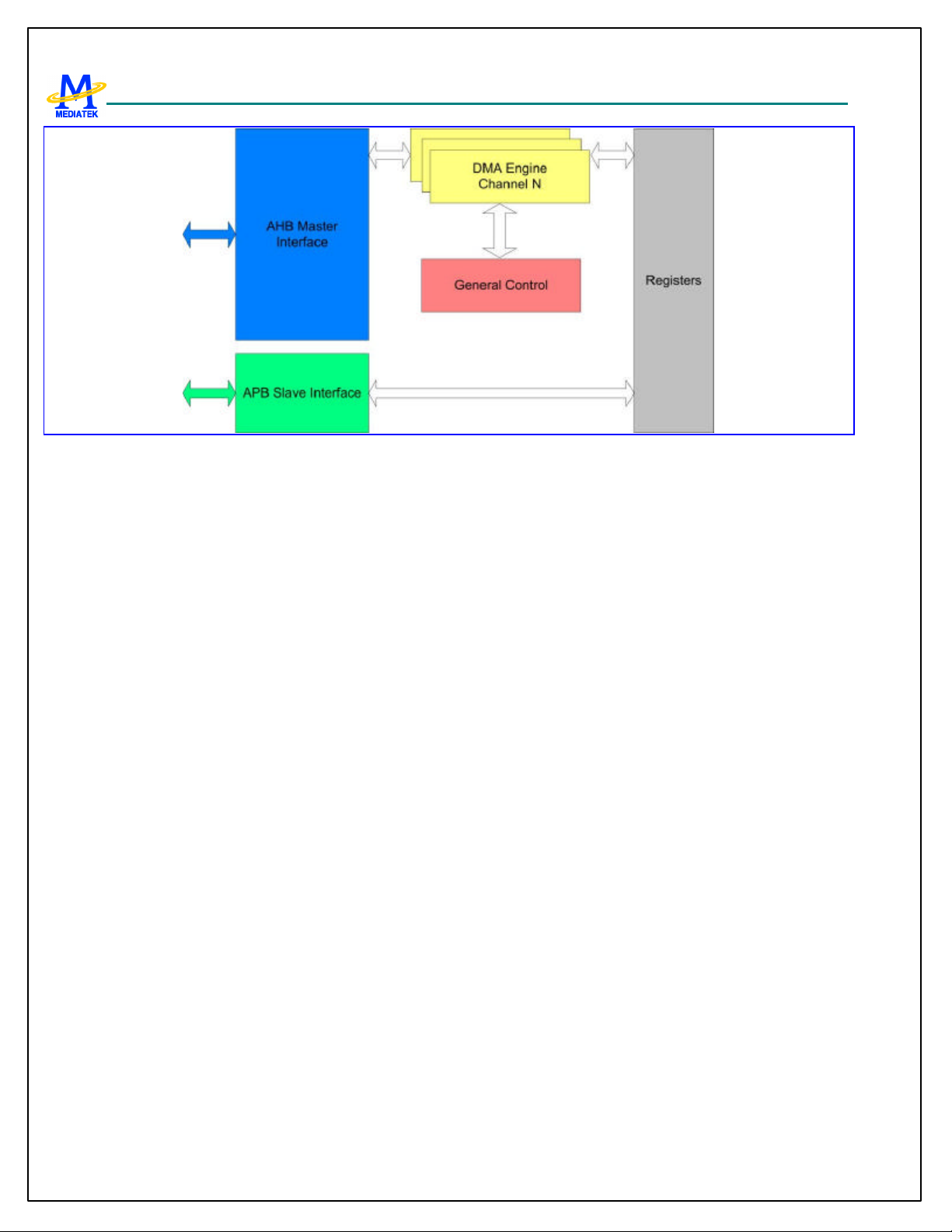
MT6217 GSM/GPRS Baseband Processor Data Sheet Revision 1.01
Figure 9 Block Diagram of Direct memory Access Module
3.4.1.1 Full-Size & Half-Size DMA Channels
There are two types of DMA channels in the DMA controller. The first one is called full-size DMA channel, and the second
one is called half-size DMA channel. Channel 1 to 3 are full-size DMA channels, and channel 4 to 9 are half-size ones. The
difference between the two types of DMA channels is that both source and destination address are programmable in
full-size DMA channels, but only one side of address can be programmed in half -size DMA channel. This can be source or
destination address. The addresses of the other sides are preset. Which preset address is used depends on the setting of MAS
in DMA Channel Control Register. See the section of Register Definition for the detail.
3.4.1.2 Ring Buffer & Double Buffer Memory Data Movement
DMA channel 1-9 support ring-buffer and double-buffer memory data movement. This can be achieved by programming
DMA_WPPT and DMA_WPTO, as well as set WPEN in DMA_CON register enable. Figure 10 illustrates how this
function works. Once transfer counter reaches the value of WPPT, next address will jump to WPTO address after
completing data transfer of WPPT. Note that there is only one side can be configured as ring-buffer or two -buffer memory,
and this is controlled by WPSD in DMA_CON register.
44/349 MediaTek Inc. Confidential
Page 45

MT6217 GSM/GPRS Baseband Processor Data Sheet Revision 1.01
Figure 10 Ring Buffer and double Buffer Memory Data Movement
3.4.1.3 Unaligned Word Access
The address of word access on AHB bus must be aligned to word boundary, or the 2 LSB will be truncated to 00b. If
programmers don’t notice that, it may cause incorrect data fetch. For the case of moving data from unaligned addresses to
aligned addresses, it’s usually done by splitting the word into four bytes, and moves it by byte. This cause four read and
four write transfers on bus. To improve b us efficiency, unaligned-word access is provided in DMA 4-9.
While this function is enable. DMAs move data from unaligned address to aligned address by executing four continuous
byte-read access and one word -write access, and vice versa. This reduces three transfers on bus.
Figure 11 unaligned word accesses
3.4.1.4 Virtual FIFO DMA
Virtual FIFO DMA is used to ease UART control. The difference between the Virtual FIFO DMAs and the ordinary DMAs
is additional FIFO controller is designed in DMA. The read and write pointer are kept in Virtual FIFO DMA. Once READ
45/349 MediaTek Inc. Confidential
Page 46

MT6217 GSM/GPRS Baseband Processor Data Sheet Revision 1.01
to this FIFO occurs, the read pointer will points to the address of the next data. On the contrary, the write pointer move to
the next address while Write to this FIFO occurs. If FIFO is empty, a FIFO read will not be allowed. In the same way, data
won’t be written into FIFO if FIFO is full. For the reason of the requirement of UART flow control, an alert length shall be
programmed. Once the FIFO Space is less than this value. An alert signal will issue to enable UART flow control. What
kinds of flow control will be taken is depend on the setting in UART.
Each Virtual FIFO DMA can be programmed as RX or TX FIFO. This depends on the setting of DIR in DMA_CON
register. If DIR is “0”(READ), it means TX FIFO. On the contrary, if DIR is “1”(WRITE), the Virtual FIFO DMA is
specified as a RX FIFO.
Virtual FIFO DMA provides an interrupt to MCU. This interrupt is to inform MCU that there are data in the FIFO, and the
amount of data is over or under the value defined in DMA_COUNT register. With this, MCU doesn’t need to poll DMA to
know when it needs to remove the data from FIFO or put data into FIFO.
Note that Virtual FIFO DMAs can’t be used as generic DMAs, i.e. DMA1-9.
Figure 12 Virtual FIFO DMA
DMA number Address of Virtual FIFO Access Port Associated UART
DMA10 7800_0000h UART1 RX / ALL UART TX
DMA11 7800_0100h UART2 RX / ALL UART TX
DMA12 7800_0200h UART3 RX / ALL UART TX
DMA13 7800_0300h ALL UART TX
Table 7 Virtual FIFO Access Port
DMA number Type Ring Buffer Two Buffer Burst Mode
DMA1 Full Size ? ? ?
DMA2 Full Size ? ? ?
DMA3 Full Size ? ? ?
DMA4 Half Size ? ? ? ?
DMA5 Half Size ? ? ? ?
DMA6 Half Size ? ? ? ?
Unaligned Word
Access
46/349 MediaTek Inc. Confidential
Page 47

MT6217 GSM/GPRS Baseband Processor Data Sheet Revision 1.01
DMA7 Half Size ? ? ? ?
DMA8 Half Size ? ? ? ?
DMA9 Half Size ? ? ? ?
DMA10 Virtual FIFO ?
DMA11 Virtual FIFO ?
DMA12 Virtual FIFO ?
DMA13 Virtual FIFO ?
Table 8 Function list of DMA channels
REGISTER ADDRESS REGISTER NAME SYNONYM
DMA + 0000h DMA Global Status Register DMA_GLBSTA
DMA + 0100h DMA Channel 1 Source Address Register DMA1_SRC
DMA + 0104h DMA Channel 1 Destination Address Register DMA1_DST
DMA + 0108h DMA Channel 1 Wrap Point Address Register DMA1_WPPT
DMA + 010Ch DMA Channel 1 Wrap To Address Register DMA1_WPTO
DMA + 0110h DMA Channel 1 Transfer Count Register DMA1_COUNT
DMA + 0114h DMA Channel 1 Control Register DMA1_CON
DMA + 0118h DMA Channel 1 Start Register DMA1_START
DMA + 011Ch DMA Channel 1 Interrupt Status Register DMA1_INTSTA
DMA + 0120h DMA Channel 1 Interrupt Acknowledge Register DMA1_ACKINT
DMA + 0124h DMA Channel 1 Remaining Length of Current Transfer DMA1_RLCT
DMA + 0128h DMA Channel 1 Bandwidth Limiter Register DMA1_LIMITER
DMA + 0200h DMA Channel 2 Source Address Register DMA2_SRC
DMA + 0204h DMA Channel 2 Destination Address Register DMA2_DST
DMA + 0208h DMA Channel 2 Wrap Point Address Register DMA2_WPPT
DMA + 020Ch DMA Channel 2 Wrap To Address Register DMA2_WPTO
DMA + 0210h DMA Channel 2 Transfer Count Register DMA2_COUNT
DMA + 0214h DMA Channel 2 Control Register DMA2_CON
DMA + 0218h DMA Channel 2 Start Register DMA2_START
DMA + 021Ch DMA Channel 2 Interrupt Status Register DMA2_INTSTA
DMA + 0220h DMA Channel 2 Interrupt Acknowledge Register DMA2_ACKINT
DMA + 0224h DMA Channel 2 Remaining Length of Current Transfer DMA2_RLCT
DMA + 0228h DMA Channel 2 Bandwidth Limiter Register DMA2_LIMITER
DMA + 0300h DMA Channel 3 Source Address Register DMA3_SRC
DMA + 0304h DMA Channel 3 Destination Address Register DMA3_DST
DMA + 0308h DMA Channel 3 Wrap Point Address Register DMA3_WPPT
DMA + 030Ch DMA Channel 3 Wrap To Address Register DMA3_WPTO
DMA + 0310h DMA Channel 3 Transfer Count Register DMA3_COUNT
DMA + 0314h DMA Channel 3 Control Register DMA3_CON
47/349 MediaTek Inc. Confidential
Page 48

MT6217 GSM/GPRS Baseband Processor Data Sheet Revision 1.01
DMA + 0318h DMA Channel 3 Start Register DMA3_START
DMA + 031Ch DMA Channel 3 Interrupt Status Register DMA3_INTSTA
DMA + 0320h DMA Channel 3 Interrupt Acknowledge Register DMA3_ACKINT
DMA + 0324h DMA Channel 3 Remaining Length of Current Transfer DMA3_RLCT
DMA + 0328h DMA Channel 3 Bandwidth Limiter Register DMA3_LIMITER
DMA + 0408h DMA Channel 4 Wrap Point Address Register DMA4_WPPT
DMA + 040Ch DMA Channel 4 Wrap To Address Register DMA4_WPTO
DMA + 0410h DMA Channel 4 Transfer Count Register DMA4_COUNT
DMA + 0414h DMA Channel 4 Control Register DMA4_CON
DMA + 0418h DMA Channel 4 Start Register DMA4_START
DMA + 041Ch DMA Channel 4 Interrupt Status Register DMA4_INTSTA
DMA + 0420h DMA Channel 4 Interrupt Ackn owledge Register DMA4_ACKINT
DMA + 0424h DMA Channel 4 Remaining Length of Current Transfer DMA4_RLCT
DMA + 0428h DMA Channel 4 Bandwidth Limiter Register DMA4_LIMITER
DMA + 042Ch DMA Channel 4 Programmable Address Register DMA4_PGMADDR
DMA + 0508h DMA Channel 5 Wrap Point Address Register DMA5_WPPT
DMA + 050Ch DMA Channel 5 Wrap To Address Register DMA5_WPTO
DMA + 0510h DMA Channel 5 Transfer Count Register DMA5_COUNT
DMA + 0514h DMA Channel 5 Control Register DMA5_CON
DMA + 0518h DMA Channel 5 Start Register DMA5_START
DMA + 051Ch DMA Channel 5 Interrupt Status Register DMA5_INTSTA
DMA + 0520h DMA Channel 5 Interrupt Acknowledge Register DMA5_ACKINT
DMA + 0524h DMA Channel 5 Remaining Length of Current Transfer DMA5_RLCT
DMA + 0528h DMA Channel 5 Bandwidth Limiter Register DMA5_LIMITER
DMA + 052Ch DMA Channel 5 Programmable Address Register DMA5_PGMADDR
DMA + 0608h DMA Channel 6 Wrap Point Address Register DMA6_WPPT
DMA + 060Ch DMA Channel 6 Wrap To Address Register DMA6_WPTO
DMA + 0610h DMA Channel 6 Transfer Count Register DMA6_COUNT
DMA + 0614h DMA Channel 6 Control Register DMA6_CON
DMA + 0618h DMA Channel 6 Start Register DMA6_START
DMA + 061Ch DMA Channel 6 Interrupt Status Register DMA6_INTSTA
DMA + 0620h DMA Channel 6 Interrupt Acknowledge Register DMA6_ACKINT
DMA + 0624h DMA Channel 6 Remaining Length of Current Transfer DMA6_RLCT
DMA + 0628h DMA Channel 6 Bandwidth Limiter Register DMA6_LIMITER
DMA + 062Ch DMA Channel 6 Programmable Address Register DMA6_PGMADDR
DMA + 0708h DMA Channel 7 Wrap Point Address Register DMA7_WPPT
DMA + 070Ch DMA Channel 7 Wrap To Address Register DMA7_WPTO
DMA + 0710h DMA Channel 7 Transfer Count Register DMA7_COUNT
DMA + 0714h DMA Channel 7 Control Register DMA7_CON
48/349 MediaTek Inc. Confidential
Page 49

MT6217 GSM/GPRS Baseband Processor Data Sheet Revision 1.01
DMA + 0718h DMA Channel 7 Start Register DMA7_START
DMA + 071Ch DMA Channel 7 Interrupt Status Register DMA7_INTSTA
DMA + 0720h DMA Channel 7 Interrupt Acknowledge Register DMA7_ACKINT
DMA + 0724h DMA Channel 7 Remaining Length of Current Transfer DMA7_RLCT
DMA + 0728h DMA Ch annel 7 Bandwidth Limiter Register DMA7_LIMITER
DMA + 072Ch DMA Channel 7 Programmable Address Register DMA7_PGMADDR
DMA + 0808h DMA Channel 8 Wrap Point Address Register DMA8_WPPT
DMA + 080Ch DMA Channel 8 Wrap To Address Register DMA8_WPTO
DMA + 0810h DMA Channel 8 Transfer Count Register DMA8_COUNT
DMA + 0814h DMA Channel 8 Control Register DMA8_CON
DMA + 0818h DMA Channel 8 Start Register DMA8_START
DMA + 081Ch DMA Channel 8 Interrupt Status Register DMA8_INTSTA
DMA + 0820h DMA Channel 8 Interrupt Acknowledge Register DMA8_ACKINT
DMA + 0824h DMA Channel 8 Remaining Length of Current Transfer DMA8_RLCT
DMA + 0828h DMA Channel 8 Bandwidth Limiter Register DMA8_LIMITER
DMA + 082Ch DMA Channel 8 Programmable Address Register DMA8_PGMADDR
DMA + 0908h DMA Channel 9 Wrap Point Address Register DMA9_WPPT
DMA + 090Ch DMA Channel 9 Wrap To Address Register DMA9_WPTO
DMA + 0910h DMA Channel 9 Transfer Count Register DMA9_COUNT
DMA + 0914h DMA Channel 9 Control Register DMA9_CON
DMA + 0918h DMA Channel 9 Start Register DMA9_START
DMA + 091Ch DMA Channel 9 Interrupt Status Register DMA9_INTSTA
DMA + 0920h DMA Channel 9 Interrupt Acknowledge Register DMA9_ACKINT
DMA + 0924h DMA Channel 9 Remaining Length of Current Transfer DMA9_RLCT
DMA + 0928h DMA Channel 9 Bandwidth Limiter Register DMA9_LIMITER
DMA + 092Ch DMA Channel 9 Programmable Address Register DMA9_PGMADDR
DMA + 0A10h DMA Channel 10 Transfer Count Register DMA10_COUNT
DMA + 0A14h DMA Channel 10 Control Register DMA10_CON
DMA + 0A18h DMA Channel 10 Start Register DMA10_START
DMA + 0A1Ch DMA Channel 10 Interrupt Status Register DMA10_INTSTA
DMA + 0A20h DMA Channel 10 Interrupt Acknowledge Register DMA10_ACKINT
DMA + 0A28h DMA Channel 10 Bandwidth Limiter Register DMA10_LIMITER
DMA + 0A2Ch DMA Channel 10 Programmable Address Register DMA10_PGMADDR
DMA + 0A30h DMA Channel 10 Write Pointer DMA10_WRPTR
DMA + 0A34h DMA Channel 10 Read Pointer DMA10_RDPTR
DMA + 0A38h DMA Channel 10 FIFO Count DMA10_FFCNT
DMA + 0A3Ch DMA Channel 10 FIFO Status DMA10_FFSTA
DMA + 0A40h DMA Channel 10 Alert Length DMA10_ALTLEN
DMA + 0A44h DMA Channel 10 FIFO Size DMA10_FFSIZE
49/349 MediaTek Inc. Confidential
Page 50

MT6217 GSM/GPRS Baseband Processor Data Sheet Revision 1.01
DMA + 0B10h DMA Channel 11 Transfer Count Register DMA11_COUNT
DMA + 0B14h DMA Channel 11 Control Register DMA11_CON
DMA + 0B18h DMA Channel 11 Start Register DMA11_START
DMA + 0B1Ch DMA Channel 11 Interrupt Status Register DMA11_INTSTA
DMA + 0B20h DMA Channel 11 Interrupt Acknowledge Register DMA11_ACKINT
DMA + 0B28h DMA Channel 11 Bandwidth Limiter Register DMA11_LIMITER
DMA + 0B2Ch DMA Channel 11 Programmable Address Register DMA11_PGMADDR
DMA + 0B30h DMA Channel 11 Write Pointer DMA11_WRPTR
DMA + 0B34h DMA Channel 11 Read Pointer DMA11_RDPTR
DMA + 0B38h DMA Channel 11 FIFO Count DMA11_FFCNT
DMA + 0B3Ch DMA Channel 11 FIFO Status DMA11_FFSTA
DMA + 0B40h DMA Channel 11 Alert Length DMA11_ALTLEN
DMA + 0B44h DMA Channel 11 FIFO Size DMA11_FFSIZE
DMA + 0C10h DMA Channel 12 Transfer Count Register DMA12_COUNT
DMA + 0C14h DMA Channel 12 Control Register DMA12_CON
DMA + 0C18h DMA Channel 12 Start Register DMA12_START
DMA + 0C1Ch DMA Channel 12 Interrupt Status Register DMA12_INTSTA
DMA + 0C20h DMA Channel 12 Interrupt Acknowledge Register DMA12_ACKINT
DMA + 0C28h DMA Channel 12 Bandwidth Limiter Register DMA12_LIMITER
DMA + 0C2Ch DMA Channel 12 Programmable Address Register DMA12_PGMADDR
DMA + 0C30h DMA Channel 12 Write Pointer DMA12_WRPTR
DMA + 0C34h DMA Channel 12 Read Pointer DMA12_RDPTR
DMA + 0C38h DMA Channel 12 FIFO Count DMA12_FFCNT
DMA + 0C3Ch DMA Channel 12 FIFO Status DMA12_FFSTA
DMA + 0C40h DMA Channel 12 Alert Length DMA12_ALTLEN
DMA + 0C44h DMA Channel 12 FIFO Size DMA12_FFSIZE
DMA + 0D10h DMA Channel 13 Transfer Count Register DMA13_COUNT
DMA + 0D14h DMA Channel 13 Control Register DMA13_CON
DMA + 0D18h DMA Channel 13 Start Register DMA13_START
DMA + 0D1Ch DMA Channel 13 Interrupt Status Register DMA13_INTSTA
DMA + 0D20h DMA Channel 13 Interrupt Acknowledge Register DMA13_ACKINT
DMA + 0D28h DMA Channel 13 Bandwidth Limiter Register DMA13_LIMITER
DMA + 0D2Ch DMA Channel 13 Programmable Address Register DMA13_PGMADDR
DMA + 0D30h DMA Channel 13 Write Pointer DMA13_WRPTR
DMA + 0D34h DMA Channel 13 Read Pointer DMA13_RDPTR
DMA + 0D38h DMA Channel 13 FIFO Count DMA13_FFCNT
DMA + 0D3Ch DMA Channel 13 FIFO Status DMA13_FFSTA
DMA + 0D40h DMA Channel 13 Alert Length DMA13_ALTLEN
DMA + 0D44h DMA Channel 13 FIFO Size DMA13_FFSIZE
50/349 MediaTek Inc. Confidential
Page 51

MT6217 GSM/GPRS Baseband Processor Data Sheet Revision 1.01
Table 9 DMA Controller Register Map
3.4.2 Register Definitions
Registers programming tips,
l Start registers shall be cleared, when associated channels are being programmed.
l PGMADDR, i.e. programmable address, only exists in half -size DMA channels. If DIR in Control Register is high,
PGMADDR represents Destination Address. On the contrary, it represents Source Address.
l Functions of ring -buffer & double -buffer memory data movement can be activated in either source side or
destination side by programming DMA_WPPT & and DMA_WPTO, as well as setting WPEN in DMA_CON
register high. WPSD in DMA_CON register determines the activated side.
DMA+0000h DMA Global Status Register DMA_GLBSTA
Bit 31 30 29 28 27 26 25 24 23 22 21 20 19 18 17 16
Name IT13
Type RO RO RO RO RO RO RO RO RO RO
Reset 0 0 0 0 0 0 0 0 0 0
Bit 15 14 13 12 11 10 9 8 7 6 5 4 3 2 1 0
Name IT8 RUN8 IT7 RUN7 IT6 RUN6 IT5 RUN5 IT4 RUN4 IT3 RUN3 IT2 RUN2 IT1 RUN1
Type R O RO RO RO RO RO RO RO RO RO RO RO RO RO RO RO
Reset 0 0 0 0 0 0 0 0 0 0 0 0 0 0 0 0
RUN1
3
IT12
RUN1
2
IT11
RUN1
1
IT10
RUN1
0
IT9 RUN9
This register helps software program being well aware of the global status of DMA channels.
RUNN DMA channel n status
0 Channel n is stopped or has completed the transfer already.
1 Channel n is currently running.
ITN Interrupt status for channel n
0 No interrupt is generated.
1 An interrupt is pending and waiting for service.
DMA+0n00h DMA Channel n Source Address Register DMAn_SRC
Bit 31 30 29 28 27 26 25 24 23 22 21 20 19 18 17 16
Name
Type R/W
Reset
Bit 15 14 13 12 11 10 9 8 7 6 5 4 3 2 1 0
Name
Type R/W
Reset
The above registers are to prompt the base or current address that a DMA channel is dealing with currently. In regard to a
write to this register, it specifies the base address of transfer source for a DMA channel. Before being able to program these
registers, the software program should be sure of that STR in DMAn_START is set to ‘0’, that is the DMA channel is
stopped and disabled completely. Other wise, the DMA channel may run out of order. In regard to a read to this set, it shows
the value exactly the same as the one being written while SINC in DMAn_CON is set to “0”. With SINC being set to “1”, it
SRC[31:16]
0
SRC[15:0]
0
51/349 MediaTek Inc. Confidential
Page 52

MT6217 GSM/GPRS Baseband Processor Data Sheet Revision 1.01
appears the current source address that the data being getting from. It allows software program being well tracking the
progress of DMA transfer.
Note that n is from 1 to 3.
SRC SRC[31:0] specifies the base or current address of transfer source for a DMA channel, i.e. channel 1, 2 or 3
WRITE base address of transfer source
READ base address of transfer source if SINC in DMAn_CON is “0”
current address of transfer source if SINC in DMAn_CON is “1”
DMA+0n04h DMA Channel n Destination Address Register DMAn_DST
Bit 31 30 29 28 27 26 25 24 23 22 21 20 19 18 17 16
Name
Type R/W
Reset
Bit 15 14 13 12 11 10 9 8 7 6 5 4 3 2 1 0
Name
Type R/W
Reset
The above registers are to index the base or current address that a DMA channel is dealing with currently. In regard to a
write to this set, it specifies the base address of the transfer destination for a DMA channel. Before being able to program
these register, the software should be sure of that STR in DMAn_START is set to ‘0’, that is the DMA channel is stopped
and disabled completely. Other wise, the DMA channel may run out of order. In regard to a read to this set, it shows the
value exactly the same as the one being written while DINC in DMAn_CON is set to “0”. With DINC being set to “1”, it
appears the current destination address that the data being sending to. It allows software program being well tracking the
progress of DMA transfer.
DST[31:16]
0
DST[15:0]
0
Note that n is from 1 to 3.
DST DST[31:0] specifies the base or current address of transfer destination for a DMA channel, i.e. channel 1, 2 or 3.
WRITE base address of transfer destination
READ base address of transfer destination if DINC in DMAn_CON is “0”
current address of transfer destination if DINC in DMAn_CON is “1”
DMA+0n08h DMA Channel n Wrap Point Count Register DMAn_WPPT
Bit 31 30 29 28 27 26 25 24 23 22 21 20 19 18 17 16
Name
Type
Reset
Bit 15 14 13 12 11 10 9 8 7 6 5 4 3 2 1 0
Name
Type R/W
Reset
The above registers are to specify the transfer count before the jump point. This can be used to support ring buffer or double
buffer style memory accesses. To enable this function, two control bit, WPEN and WPSD, in DMA control register should
be programmed. See following register description for the detail. While transfer counter in DMA engine matches this
address, an address ju mp will occurs, and the next address will be the address specified in DMAn_WPTO. Before being
able to program these register, the software should be sure of that STR in DMAn_START is set to ‘0’, that is the DMA
WPPT[15:0]
0
52/349 MediaTek Inc. Confidential
Page 53

MT6217 GSM/GPRS Baseband Processor Data Sheet Revision 1.01
channel is stopped and disabled completely. Other wise, the DMA channel may run out of order. To enable this function,
WPEN in DMA_CON should be set.
Note that n is from 1 to 9.
WPPT WPPT[15:0] specifies the amount of the transfer count from start to jumping point for a DMA channel, i.e.
channel 1 – 9.
WRITE the address of the jump point.
READ the same as what you fill in.
DMA+0n0Ch DMA Channel n Wrap To Address Register DMAn_WPTO
Bit 31 30 29 28 27 26 25 24 23 22 21 20 19 18 17 16
Name
Type R/W
Reset
Bit 15 14 13 12 11 10 9 8 7 6 5 4 3 2 1 0
Name
Type R/W
Reset
The above registers are to specify the address of the jump destination of a given DMA transfer to support ring buffer or
double buffer style memory accesses. To enable this function, two con trol bit, WPEN and WPSD, in DMA control register
should be programmed. See following register description for the detail. Before being able to program these register, the
software should be sure of that STR in DMAn_START is set to ‘0’, that is the DMA channel is stopped and disabled
completely. Other wise, the DMA channel may run out of order. To enable this function, WPEN in DMA_CON should be
set.
WPTO[31:16]
0
WPTO[15:0]
0
Note that n is from 1 to 9.
WPTO WPTO[31:0] specifies the address of the jump point for a DMA channel, i.e. channel 1 – 11.
WRITE the address of the jump destination.
READ the same as what you fill in.
DMA+0n10h DMA Channel n Transfer Count Register DMAn_COUNT
Bit 31 30 29 28 27 26 25 24 23 22 21 20 19 18 17 16
Name
Type
Reset
Bit 15 14 13 12 11 10 9 8 7 6 5 4 3 2 1 0
Name
Type R/W
Reset
This register specifies the amount of total transfer count that the DMA channel is required to perform. Upon completion, the
DMA channel generates an interrupt request to the processor while ITEN in DMAn_CON is set as ‘1’. Note that the total
size of data being transferred by a DMA channel is determined by LEN together with the SIZE in DMAn_CON, i.e. LEN x
SIZE.
For virtual FIFO DMA, this register is u sed to configure the RX threshold and TX threshold. Interrupt is triggered while
FIFO count >= RX threshold in RX path or FIFO count =< TX threshold in TX path. Note that ITEN bit in DMA_CON
register shall be set, or no interrupt will issue.
LEN
0
53/349 MediaTek Inc. Confidential
Page 54

MT6217 GSM/GPRS Baseband Processor Data Sheet Revision 1.01
Note that n is from 1 to 13.
LEN The amount of total transfer count
DMA+0n14h DMA Channel n Control Register DMAn _CON
Bit 31 30 29 28 27 26 25 24 23 22 21 20 19 18 17 16
Name MAS DIR WPEN WPSD
Type R/W R/W R/W R/W
Reset 0 0 0 0
Bit 15 14 13 12 11 10 9 8 7 6 5 4 3 2 1 0
Name ITEN BURST B2W DRQ DINC SINC SIZE
Type R/W R/W R/W R/W R/W R/W R/W
Reset 0 0 0 0 0 0 0
This register appeals all the available control schemes for a DMA channel that is ready for software programmer to
configure with. Note that all these fields cannot be changed while DMA transfer is in progress or unexpected situation may
occur.
Note that n is from 1 to 13.
SIZE Data size within the confine of a bus cycle per transfer
These bits confines the size to the specified value for individual bus cycle that data is moving between source and
destination. The size is in terms of byte and has maximum value of 4 bytes. It is mainly decided by the data width
of a DMA master.
00 Byte transfer/1 byte
01 Half-word transfer/2 bytes
10 Word transfer/4 bytes
11 Reserved
SINC Appearance control for the source address registers DMAn_MSBSRC and DMAn_LSBSRC
0 The base address of the source
1 The current address of the source that the DMA channel is currently dealing with.
DINC Appearance control for the destination address registers DMAn_MSBDST and DMAn_LSBDST
0 The base address of the destination
1 The current address of the destination that the DMA channel is currently dealing with
DREQ Throttle and handshake control for DMA transfer
0 No throttle control during DMA transfer or transfers occurred only between memories
1 Hardware handshake management
The DMA master is able to throttle down the transfer rate by way of request-grant handshake.
B2W Word to Byte or Byte to Word transfer for the applications of transferring non-word-aligned-address data to
word-aligned-address data. Note that BURST shall be set to 4-beat burst while enabling this function, and the
SIZE shall be set to Byte.
NO effect on channel 1 – 3 & 10 - 13.
0 Disable
1 Enable
BURST Transfer Type. Burst-type transfers have better bus efficiency. Massy data movement is recommended to use this
kind of transfer. But note that burst-type transfer won’t stop until all of the beats are completed or transfer length is
reached. FIFO threshold of peripherals shall be configured carefully while you use it to move data from/to this
peripheral.
54/349 MediaTek Inc. Confidential
Page 55

MT6217 GSM/GPRS Baseband Processor Data Sheet Revision 1.01
What transfer type can be used is restricted by the SIZE. If SIZE is 00b, i.e. byte transfer, all of the four transfer
types can be used. If SIZE is 01b, i.e. half -word transfer, 16-beat incrementing burst can’t be used. If SIZE is 10b,
i.e. word transfer, only single and 4-beat incrementing burst can be used.
NO effect on channel 10 - 13.
000 Single
001 Reserved
010 4-beat incrementing burst
011 Reserved
100 8-beat incrementing burst
101 Reserved
110 16-beat incrementing burst
111 Reserved
ITEN DMA transfer completion interrupt enable.
0 Disable
1 Enable
WPSD The side using wrap-addressing function. Only one side of a DMA channel can activate wrap-addressing function
at a time.
NO effect on channel 10 - 13.
0 wrap-addressing on source
1 wrap-addressing on destination
WPEN Wrap addressing for ring buffer. The next address of DMA jumps to WRAP TO address while current address
matches WRAP POINT address.
NO effect on channel 10 - 13.
0 Disable
1 Enable
DIR the directions of DMA transfer for half-size DMA channels, i.e. channel 4 – 11. The direction is from the
viewpoint of DMA masters. WRITE means that reads from master and then writes to the address specified in
DMA_PGMADDR. Vice versa.
NO effect on channel 1 - 3.
0 Read
1 Write
MAS Master selection. Specifying which master occupies this DMA channel. Once assigned to certain master,
corresponding DREQ and DACK will be connected. In regard to half -size DMA channels, i.e. channel 4 – 11, a
preset address will be assigned as well.
0000 SIM
0001 MSDC
0010 IrDA TX
0011 IrDA RX
0100 USB1 Write
0101 USB1 Read
0110 USB2 Write
0111 USB2 Read
1000 UART1 TX
1001 UART1 RX
55/349 MediaTek Inc. Confidential
Page 56

MT6217 GSM/GPRS Baseband Processor Data Sheet Revision 1.01
1010 UART2 TX
1011 UART2 RX
1100 UART3 TX
1101 UART3 RX
1110 DDMA
1111 NFI (full-size DMA only)
DMA+0n18h DMA Channel n Start Register DMAn_START
Bit 31 30 29 28 27 26 25 24 23 22 21 20 19 18 17 16
Name
Type
Reset
Bit 15 14 13 12 11 10 9 8 7 6 5 4 3 2 1 0
Name STR
Type R/W
Reset 0
This register controls the activity of a DMA channel. Note that prior to set STR to “1”, all the configuratio ns should be
done by giving proper value to the registers including DMAn_SRC, DMAn_DST, DMAn_PGMADDR, DMAn_COUNT
and DMAn_CON. Note also that once the STR is set to “1”, the hardware will not clear it automatically no matter the DMA
channel accomplishes th e DMA transfer or not. Put another way, the value of STR keeps as “1” in spite of the completion
of DMA transfer. Therefore, the software program should be sure to clear STR to “0” before being able to re -start another
DMA transfer.
Note that n is from 1 to 13.
STR Start control for a DMA channel
0 The DMA channel is stopped
1 The DMA channel is started and running
DMA+0n1Ch DMA Channel n Interrupt Status Register DMAn_INTSTA
Bit 31 30 29 28 27 26 25 24 23 22 21 20 19 18 17 16
Name
Type
Reset
Bit 15 14 13 12 11 10 9 8 7 6 5 4 3 2 1 0
Name INT
Type R O
Reset 0
This register shows the interrupt status of a DMA channel. In fact the value is exactly the same as in DMA_GLBSTA.
Note that n is from 1 to 13.
INT Interrupt Status for DMA Channel
0 No interrupt request is generated.
1 One interrupt request is pending and waiting for service
DMA+0n20h DMA Channel n Interrupt Acknowledge Register DMAn_ACKINT
Bit 31 30 29 28 27 26 25 24 23 22 21 20 19 18 17 16
Name
Type
56/349 MediaTek Inc. Confidential
Page 57

MT6217 GSM/GPRS Baseband Processor Data Sheet Revision 1.01
Reset
Bit 15 14 13 12 11 10 9 8 7 6 5 4 3 2 1 0
Name ACK
Type WO
Reset 0
This register is used to acknowledge the current interrupt request associated with the completion event of a DMA channel
by software program. Note that this is a write-only register, any read to it will return a value of “0”.
Note that n is from 1 to 13.
ACK Interrupt acknowledge for the DMA channel
0 No effect
1 Interrupt request is acknowledged and should be relinquished.
DMA+0n24h DMA Channel n Remaining Length of Current Transfer DMAn_RLCT
Bit 31 30 29 28 27 26 25 24 23 22 21 20 19 18 17 16
Name
Type
Reset
Bit 15 14 13 12 11 10 9 8 7 6 5 4 3 2 1 0
Name
Type RO
Reset
RLCT
0
This register is to reflect the left amount of the transfer.
Note that n is from 1 to 9
DMA+0n28h DMA Bandwidth limiter Register DMAn_LIMITER
Bit 31 30 29 28 27 26 25 24 23 22 21 20 19 18 17 16
Name
Type
Reset
Bit 15 14 13 12 11 10 9 8 7 6 5 4 3 2 1 0
Name LIMITER
Type R/W
Reset 0
This register is to suppress the Bus utilization of the DMA channel. The value is from 0 to 255. 0 means no limitation, and
255 means totally banned. The value between 0 and 255 means certain DMA can has permission to use AHB every (4 X n)
AHB clock cycles.
Note that it’s not recommended to limit the Bus utilization of the DMA channels because this will increase the latency of
response to the masters, and the transfer rate will decrease as well. Before using it, programmer must make sure that
masters have some protective mechanism to avoid going into wrong state.
Note that n is from 1 to 13.
LIMITER from 0 to 255. 0 means no limitation, 255 means totally banned, and others means Bus access permission
every (4 X n) AHB clock.
57/349 MediaTek Inc. Confidential
Page 58

MT6217 GSM/GPRS Baseband Processor Data Sheet Revision 1.01
DMA+0n2Ch DMA Channel n Programmable Address Register
Bit 31 30 29 28 27 26 25 24 23 22 21 20 19 18 17 16
Name
Type R/W
Reset
Bit 15 14 13 12 11 10 9 8 7 6 5 4 3 2 1 0
Name
Type R/W
Reset
The above registers are to specify the address for a half -size DMA channel. This address represents source address if DIR in
DMA_CON is set to 0, and on the contrary it represents destination address. Before being able to program these register,
the software shou ld be sure of that STR in DMAn_START is set to ‘0’, that is the DMA channel is stopped and disabled
completely. Other wise, the DMA channel may run out of order. To enable this function, a control bit in DMA control
register should
Note that n is from 4 to 11.
PGMADDR PGMADDR[31:0] specifies the address for a half -size DMA channel, i.e. channel 4 – 11.
WRITE the address of the jump destination.
READ base address of transfer destination if SINC/DINC in DMAn_CON is “0”
current address of transfer destination if SINC/DINC in DMAn_CON is “1”
PGMADDR[31:16]
0
PGMADDR[15:0]
0
R
DMAn _PGMADD
DMA+0n30h DMA Channel n Virtual FIFO Write Pointer Register DMAn_WRPTR
Bit 31 30 29 28 27 26 25 24 23 22 21 20 19 18 17 16
Name
Type RO
Bit 15 14 13 12 11 10 9 8 7 6 5 4 3 2 1 0
Name
Type RO
WRPTR[31:16]
WRPTR[15:0]
Note that n is from 10 to 13.
WRPTR Virtual FIFO Write Pointer.
DMA+0n34h DMA Channel n Virtual FIFO Read Pointer Register DMAn_RDPTR
Bit 31 30 29 28 27 26 25 24 23 22 21 20 19 18 17 16
Name
Type RO
Bit 15 14 13 12 11 10 9 8 7 6 5 4 3 2 1 0
Name
Type RO
RDPTR[31:16]
RDPTR[15:0]
Note that n is from 10 to 13.
RDPTR Virtual FIFO Read Pointer.
DMA+0n38h DMA Channel n Virtual FIFO Data Count Register DMAn_FFCNT
Bit 31 30 29 28 27 26 25 24 23 22 21 20 19 18 17 16
Name
Type
58/349 MediaTek Inc. Confidential
Page 59

MT6217 GSM/GPRS Baseband Processor Data Sheet Revision 1.01
Bit 15 14 13 12 11 10 9 8 7 6 5 4 3 2 1 0
Name
Type RO
FFCNT
Note that n is from 10 to 13.
FFCNT To display the number of data stored in FIFO. 0 means FIFO empty, and FIFO is full if FFCNT is equal to
FFSIZE.
DMA+0n3Ch DMA Channel n Virtual FIFO Status Register DMAn_FFSTA
Bit 31 30 29 28 27 26 25 24 23 22 21 20 19 18 17 16
Name
Type
Reset
Bit 15 14 13 12 11 10 9 8 7 6 5 4 3 2 1 0
Name ALT
Type RO RO RO
Reset 0 1 0
Note that n is from 10 to 13.
FULL To indicate FIFO is full.
0 Not Full
1 Full
EMPTY To indicate FIFO is empty.
0 Not Empty
1 Empty
ALT To indicate FIFO Count is larg er than ALTLEN. DMA will issue alert signal to UART to enable UART flow
control.
0 Not reach alert region
1 Reach alert region.
EMPT
Y
FULL
DMA+0n40h DMA Channel n Virtual FIFO Alert Length Register DMAn_ALTLEN
Bit 31 30 29 28 27 26 25 24 23 22 21 20 19 18 17 16
Name
Type
Reset
Bit 15 14 13 12 11 10 9 8 7 6 5 4 3 2 1 0
Name ALTLEN
Type R/W
Reset 0
Note that n is from 10 to 13.
ALTLEN specifies the Alert Length of Virt ual FIFO DMA. Once remaining FIFO space is less than ALTLEN, an alert
signal will issued to UART to enable flow control. Normally, ALTLEN shall be larger than 16 for UART
application.
DMA+0n44h DMA Channel n Virtual FIFO Size Register DMAn_FFSIZE
Bit 31 3 0 29 28 27 26 25 24 23 22 21 20 19 18 17 16
Name
59/349 MediaTek Inc. Confidential
Page 60

MT6217 GSM/GPRS Baseband Processor Data Sheet Revision 1.01
Type
Reset
Bit 15 14 13 12 11 10 9 8 7 6 5 4 3 2 1 0
Name
Type R/W
Reset
FFSIZE
0
Note that n is from 10 to 13.
FFSIZE specifies the FIFO Size of Virtual FIFO DMA.
3.5 Interrupt Controller
3.5.1 General Description
Figure 13 outlines the major functionality of the MCU Interrupt Controller. The interrupt controller processes all interrupt
sources coming from external lines and internal MCU peripherals. Since ARM7EJ-S core supports two levels of interrupt
latency, this controller will generate two request signals: FIQ for fast, low latency interrupt request and IRQ for more
general interrupts with lower priority.
EINT FIQ
TDMA
GPT
SIM
UART1
KP
RTC
UART2
DSP2MCU
APB Bus
Interrupt
Input
Multiplex
Figure 13 Block Diagram of the Interrupt Controller
IRQ0
IRQ1
IRQ2
IRQn
IRQ31
SoftIRQ
Registers
FIQ
Controller
IRQ
Controller
IRQ
One and only one of the interrupt sources can be assigned to FIQ Controller and have the highest priority in requesting
timing critical service. All the others should share the same IRQ signal by connecting them to IRQ Controller. The IRQ
Controller manages up 32 interrupt lines of IRQ0 to IRQ31 with fixed priority in descending order.
60/349 MediaTek Inc. Confidential
Page 61

MT6217 GSM/GPRS Baseband Processor Data Sheet Revision 1.01
The Interrupt Controller provides a simple software interface by mean of regis ters to manipulate the interrupt request shared
system. IRQ Selection Registers and FIQ Selection Register determine the source priority and connecting relation among
sources and interrupt lines. IRQ Source Status Register allows software program to identify the source of interrupt that
generates the interrupt request. IRQ Mask Register provides software to mask out undesired sources some time. End of
Interrupt Register permits software program to indicate the controller that a certain interrupt service routine has been
finished.
Binary coded version of IRQ Source Status Register is also made available for software program to helpfully identify the
interrupt source. Note that while taking this advantage, it should also take the binary coded version of End of Interrupt
Register coincidently.
The essential Interrupt Table of ARM7EJ-S core is shown as Table 10.
Address Description
00000000h System Reset
00000018h IRQ
0000001Ch FIQ
Table 10 Interrupt Table of ARM7EJ-S
3.5.1.1 External Interrupt
This interrupt controller also integrates an External Interrupt Controller that can support up to 4 interrupt requests coming
from external sources, the EINT0–3 as shown in Figure 14, and 4 WakeUp interru pt requests, i.e. EINT4-7, coming from
peripherals used to inform system to resume system clock.
The four external interrupts can be used for different kind of applications, mainly for event detections: detection of hand
free connection, detection of hood opening, detection of battery charger connection.
Since the external event may be unstable in a certain period, de-bounce mechanism is introduced to ensure the functionality.
The circuitry is mainly used to verify that if the input signal remains stable for a programmable number of periods of the
clock. When this condition is satisfied, for the appearance or the disappearance of the input, the output of the de-bounce
logic will change to the desired state. Note that, because it uses the 32KHz slow clock fo r doing de-bounce process, the
parameters takes effect no sooner than 1 32KHz clock cycle, ~31.25us, after software program sets them. For example of
changing the polarity of an external interrupt, a 31.25us guard time shall be applied between the two events of changing the
polarity value in EINT_CON register and End-of -Interrupt. Or an abnormal external interrupt could be triggered.
61/349 MediaTek Inc. Confidential
Page 62

MT6217 GSM/GPRS Baseband Processor Data Sheet Revision 1.01
EINT4-7
EINT3
Debounce Logic
EINT2
Debounce Logic
EINT1
Debounce Logic
EINT0
Debounce Logic
Figure 14 Block diagram of External Interrupt Controller
REGISTER ADDRESS REGISTER NAME SYNONYM
CIRQ + 0000h IRQ Selection 0 Register IRQ_SEL0
CIRQ + 0004h IRQ Selection 1 Register IRQ_SEL1
CIRQ + 0008h IRQ Selection 2 Register IRQ_SEL2
CIRQ + 000Ch IRQ Selection 3 Register IRQ_SEL3
CIRQ + 0010h IRQ Selection 4 Register IRQ_SEL4
CIRQ + 0014h IRQ Selection 5 Register IRQ_SEL5
CIRQ + 0018h FIQ Selection Register FIQ_SEL
Registers
Interrupt
Control
Logic
MT6217
EINT_IRQ
APB Bus
CIRQ + 001Ch IRQ Mask Register IRQ_MASK
CIRQ + 0020h IRQ Mask Disable Register IRQ_MASK_DIS
CIRQ + 0024h IRQ Mask Enable Register IRQ_MASK_EN
CIRQ + 0028h IRQ Status Register IRQ_STA
CIRQ + 002Ch IRQ End of Interrupt Register IRQ_EOI
CIRQ + 0030h IRQ Sensitive Register IRQ_SENS
CIRQ + 0034h IRQ Software Interrupt Register IRQ_SOFT
CIRQ + 0038h FIQ Control Register FIQ_CON
CIRQ + 003Ch FIQ End of Interrupt Register FIQ_EOI
CIRQ + 0040h Binary Coded Value of IRQ_STATUS IRQ_STA2
CIRQ + 0044h Binary Coded Value of IRQ_EOI IRQ_EOI2
CIRQ + 0100h EINT Status Register EINT_STA
CIRQ + 0104h EINT Mask Register EINT_MASK
CIRQ + 0108h EINT Mask Disable Register EINT_MASK_DIS
CIRQ + 010Ch EINT Mask Enable Register EINT_MASK_EN
62/349 MediaTek Inc. Confidential
Page 63

MT6217 GSM/GPRS Baseband Processor Data Sheet Revision 1.01
CIRQ + 0110h EINT Interrupt Acknowledge Register EINT_INTACK
CIRQ + 0114h EINT Sensitive Register EINT_SENS
CIRQ + 0120h EINT0 De -bounce Control Register EINT0_CON
CIRQ + 0130h EINT1 De -bounce Control Register EINT1_CON
CIRQ + 0140h EINT2 De -bounce Control Register EINT2_CON
CIRQ + 0150h EINT3 De -bounce Control Register EINT3_CON
CIRQ + 0160h EINT4 De -bounce Control Register EINT4_CON
CIRQ + 0170h EINT5 De -bounce Control Register EINT5_CON
CIRQ + 0180h EINT6 De -bounce Control Register EINT6_CON
CIRQ + 0190h EINT7 De -bounce Control Register EINT7_CON
Table 11 Interrupt Controller Register Map
3.5.2 Register Definitions
CIRQ+0000h IRQ Selection 0 Register IRQ_SEL0
Bit 31 30 29 28 27 26 25 24 23 22 21 20 19 18 17 16
Name IRQ5 IRQ4 IRQ3
Type R/W R/W R/W
Reset 5 4 3
Bit 15 14 13 12 11 10 9 8 7 6 5 4 3 2 1 0
Name IRQ2 IRQ1 IRQ0
Type R/W R/W R/W
Reset 2 1 0
CIRQ+0004h IRQ Selection 1 Register IRQ_SEL1
Bit 31 30 29 28 27 26 25 24 23 22 21 20 19 18 17 16
Name IRQB IRQA IRQ9
Type R/W R/W R/W
Reset B A 9
Bit 15 14 13 12 11 10 9 8 7 6 5 4 3 2 1 0
Name IRQ8 IRQ7 IRQ6
Type R/W R/W R/W
Reset 8 7 6
CIRQ+0008h IRQ Selection 2 Register IRQ_SEL2
Bit 31 30 29 28 27 26 25 24 23 22 21 20 19 18 17 16
Name IRQ11 IRQ10 IRQF
Type R/W R/W R/W
Reset 11 10 F
Bit 15 14 13 12 11 10 9 8 7 6 5 4 3 2 1 0
Name IRQE IRQD IRQC
Type R/W R/W R/W
Reset E D C
CIRQ+000Ch IRQ Selection 3 Register IRQ_SEL3
Bit 31 30 29 28 27 26 25 24 23 22 21 20 19 18 17 16
63/349 MediaTek Inc. Confidential
Page 64

MT6217 GSM/GPRS Baseband Processor Data Sheet Revision 1.01
Name IRQ17 IRQ16 IRQ15
Type R/W R/W R/W
Reset 17 16 15
Bit 15 14 13 12 11 10 9 8 7 6 5 4 3 2 1 0
Name IRQ14 IRQ13 IRQ12
Type R/W R/W R/W
Reset 14 13 12
CIRQ+0010h IRQ Selection 4 Register IRQ_SEL4
Bit 31 30 29 28 27 26 25 24 23 22 21 20 19 18 17 16
Name IRQ1D IRQ1C IRQ1B
Type R/W R/W R/W
Reset 1D 1C 1B
Bit 15 14 13 12 11 10 9 8 7 6 5 4 3 2 1 0
Name IRQ1A IRQ19 IRQ18
Type R/W R/W R/W
Reset 1A 19 18
CIRQ+0014h IRQ Selection 5 Register IRQ_SEL5
Bit 31 30 29 28 27 26 25 24 23 22 21 20 19 18 17 16
Name
Type
Reset
Bit 15 14 13 12 11 10 9 8 7 6 5 4 3 2 1 0
Name IRQ1F IRQ1E
Type R/W R/W
Reset 1F 1E
CIRQ+0018h FIQ Selection Register FIQ_SEL
Bit 31 30 29 28 27 26 25 24 23 22 21 20 19 18 17 16
Name
Type
Reset
Bit 15 14 13 12 11 10 9 8 7 6 5 4 3 2 1 0
Name FIQ
Type R/W
Reset 0
The IRQ/FIQ Selection Registers provide system designers with a flexible routing scheme to make various mappings of
priority among interrupt sources possible. It allows the interrupt sources being mapped onto interrupt requests of either FIQ
or IRQ. Where only one interrupt source can be assigned to FIQ, the other ones should share IRQ by mapping them onto
IRQ0 to IRQ1 F connected to IRQ controller. The priority of IRQ0-IRQ1F is fixed, i.e. IRQ0 > IRQ1 > IRQ2 > … > IRQ1E
> IRQ1F. During the software configuration process, the Interrupt Source Code of desired interrupt source should be
written into source field of the corresponding IRQ_SEL0-IRQ_SEL4/FIQ_SEL. 5-bit Interrupt Source Codes for all
interrupt sources are fixed and defined in Table 12.
Interrupt Source Interrupt Source Code
MFIQ 00000
TDMA_CTIRQ1 00001
TDMA_CTIRQ2 00010
64/349 MediaTek Inc. Confidential
Page 65

MT6217 GSM/GPRS Baseband Processor Data Sheet Revision 1.01
DSP2CPU 00011
SIM 00100
DMA 00101
TDMA 00110
UART1 00111
KeyPad 01000
UART2 01001
GPTimer 01010
EINT 01011
USB 01100
MSDC 01101
RTC 01110
IrDA 01111
LCD 10000
UART3 10001
MIRQ 10010
WDT 10011
JPEG 10100
Resizer 10101
NFI 10110
B2PSI 10111
Reserved 11000
Reserved 11001
Reserved 11010
Reserved 11011
Reserved 11100
Reserved 11101
Reserved 11110
Reserved 11111
Table 12 Interrupt Source Code for Interrupt Sources
FIQ, IRQ0-1F The 5-bit content of this field would b e the Interrupt Source Code shown in Table 12 indicating that the
certain interrupt source uses the associated interrupt line to generate interrupt requests.
CIRQ+001Ch IRQ Mask Register IRQ_MASK
Bit 31 30 29 28 27 26 25 24 23 22 21 20 19 18 17 16
Name IRQ1F IRQ1E IRQ1D IRQ1C IRQ1B IRQ1A IRQ19 IRQ18 IRQ17 IRQ16 IRQ15 IRQ14 IRQ13 IRQ12 IRQ11 IRQ10
Type R/W R/W R/W R/W R/W R/W R/W R/W R/W R/W R/W R/W R/W R/W R/W R/W
Reset 1 1 1 1 1 1 1 1 1 1 1 1 1 1 1 1
Bit 15 14 13 12 11 10 9 8 7 6 5 4 3 2 1 0
Name IRQF IRQE IRQD IRQC IRQB IRQA IRQ9 IRQ8 IRQ7 IRQ6 IRQ5 IRQ4 IRQ3 IRQ2 IRQ1 IRQ0
Type R/W R/W R/W R/W R/W R/W R/W R/W R/W R/W R/W R/W R/W R/W R/W R/W
Reset 1 1 1 1 1 1 1 1 1 1 1 1 1 1 1 1
65/349 MediaTek Inc. Confidential
Page 66

MT6217 GSM/GPRS Baseband Processor Data Sheet Revision 1.01
This register contains mask bit for each interrupt line in IRQ Controller. It allows each interrupt source of IRQ0 to IRQ1F
to be disabled or masked out separately under software control. After System Reset, all bit values will be set to ‘1’ to
indicate that interrupt requests are prohibited.
IRQ0-1F Mask Control for the Associated Interrupt Source in IRQ Controller
0 Interrupt is enabled
1 Interrupt is disabled
CIRQ+0020h IRQ Mask Clear Register
Bit 31 30 29 28 27 26 25 24 23 22 21 20 19 18 17 16
Name IRQ1F IRQ1E IRQ1D IRQ1C IRQ1B IRQ1A IRQ19 IRQ18 IRQ17 IRQ16 IRQ15 IRQ14 IRQ13 IRQ12 IRQ11 IRQ10
Type W1C W1C W1C W1C W1C W1C W1C W1C W1C W1C W1C W1C W1C W1C W1C W1C
Bit 15 14 13 12 11 10 9 8 7 6 5 4 3 2 1 0
Name IRQF IRQE IRQD IRQC IRQB IRQA IRQ9 IRQ8 IRQ7 IRQ6 IRQ5 IRQ4 IRQ3 IRQ2 IRQ1 IRQ0
Type W1C W1C W1C W1C W1C W1C W1C W1C W1C W1C W1C W1C W1C W1C W1C W1C
This register is used to clear bits in the IRQ Mask Register. When writing to this register, each data bit which is high will
cause the corre sponding bit in the IRQ Mask Register to be cleared. Data bits which are low have no effect on the
corresponding bits in the IRQ Mask Register
IRQ0-1F Clear corresponding bits in IRQ Mask Register.
0 no effect
1 Disable corresponding MASK bit
R
CIRQ+0024h IRQ Mask SET Register IRQ_MASK_SET
Bit 31 30 29 28 27 26 25 24 23 22 21 20 19 18 17 16
Name IRQ1F IRQ1E IRQ1D IRQ1C IRQ1B IRQ1A IRQ19 IRQ18 IRQ17 IRQ16 IRQ15 IRQ14 IRQ13 IRQ12 IRQ11 IRQ10
Type W1S W1S W1S W1S W1S W1S W1S W1S W1S W1S W1S W1S W1S W1S W1S W1S
Bit 15 14 13 12 11 10 9 8 7 6 5 4 3 2 1 0
Name IRQF IRQE IRQD IRQC IRQB IRQA IRQ9 IRQ8 IRQ7 IRQ6 IRQ5 IRQ4 IRQ3 IRQ2 IRQ1 IRQ0
Type W1S W1S W1S W1S W1S W1S W1S W1S W1S W1S W1S W1S W1S W1S W1S W1S
IRQ_MASK_CL
This register is used to set bits in the IRQ Mask Register. When writing to this register, each data bit which is high will
cause the corresponding bit in the IRQ Mask Register to be set. Data bits which are low have no effect on the corresponding
bits in the IRQ Mask Register
IRQ0-1F Set corresponding bits in IRQ Mask Register.
0 no effect
1 Enable corresponding MASK bit
CIRQ+0028h IRQ Source Status Register IRQ_STA
Bit 31 30 29 28 27 26 25 24 23 22 21 20 19 18 17 16
Name IRQ1F IRQ1E IRQ1D IRQ1C IRQ1B IRQ1A IRQ19 IRQ18 IRQ17 IRQ16 IRQ15 IRQ14 IRQ13 IRQ12 IRQ11 IRQ10
Type RC RC RC RC RC RC RC RC RC RC RC RC RC RC RC RC
Reset 0 0 0 0 0 0 0 0 0 0 0 0 0 0 0 0
Bit 15 14 13 12 11 10 9 8 7 6 5 4 3 2 1 0
Name IRQF IRQE IRQD IRQC IRQB IRQA IRQ9 IRQ8 IRQ7 IRQ6 IRQ5 IRQ4 IRQ3 IRQ2 IRQ1 IRQ0
Type RC RC RC RC RC RC RC RC RC RC RC RC RC RC RC RC
Reset 0 0 0 0 0 0 0 0 0 0 0 0 0 0 0 0
66/349 MediaTek Inc. Confidential
Page 67

MT6217 GSM/GPRS Baseband Processor Data Sheet Revision 1.01
This Register allows software to poll which interrupt line generates the IRQ interrupt request. A bit set to ‘1’ indicates a
corresponding active inte rrupt line. Only one flag is active at a time. The IRQ_STA is type of READ-ONLY, write access
will have no effect to the content.
IRQ0-1F Interrupt Indication for the Associated Interrupt Source
0 The associated interrupt source is non-active
1 The associa ted interrupt source is asserted
CIRQ+002Ch IRQ End of Interrupt Register IRQ_EOI
Bit 31 30 29 28 27 26 25 24 23 22 21 20 19 18 17 16
Name IRQ1F IRQ1E IRQ1D IRQ1C IRQ1B IRQ1A IRQ19 IRQ18 IRQ17 IRQ16 IRQ15 IRQ14 IRQ13 IRQ12 IRQ11 IRQ10
Type WO WO WO WO WO WO WO WO WO WO WO WO WO WO WO WO
Reset 0 0 0 0 0 0 0 0 0 0 0 0 0 0 0 0
Bit 15 14 13 12 11 10 9 8 7 6 5 4 3 2 1 0
Name IRQF IRQE IRQD IRQC IRQB IRQA IRQ9 IRQ8 IRQ7 IRQ6 IRQ5 IRQ4 IRQ3 IRQ2 IRQ1 IRQ0
Type WO WO WO WO WO WO WO WO WO WO WO WO WO WO WO WO
Reset 0 0 0 0 0 0 0 0 0 0 0 0 0 0 0 0
This register provides a mean for software to relinquish and refresh the Interrupt Controller. Writing a ‘1’ to the specific bit
position will result in an End of Interrupt Command internally to the corresponding interrupt line.
IRQ0-1F End of Interrupt Command for the Associated Interrupt Line
0 No service is currently in progress or pending
1 Interrupt request is in -service
CIRQ+0030h IRQ Sensitive Register IRQ_SENS
Bit 31 30 29 28 27 26 25 24 23 22 21 20 19 18 17 16
Name IRQ1F IRQ1E IRQ1D IRQ1C IRQ1B IRQ1A IRQ19 IRQ18 IRQ17 IRQ16 IRQ15 IRQ14 IRQ13 IRQ12 IRQ11 IRQ10
Type R/W R/W R/W R/W R/W R/W R/W R/W R/W R/W R/W R/W R/W R/W R/W R/W
Reset 0 0 0 0 0 0 0 0 0 0 0 0 0 0 0 0
Bit 15 14 13 12 11 10 9 8 7 6 5 4 3 2 1 0
Name IRQF IRQE IRQD IRQC IRQB IRQA IRQ9 IRQ8 IRQ7 IRQ6 IRQ5 IRQ4 IRQ3 IRQ2 IRQ1 IRQ0
Type R/W R/W R/W R/W R/W R/W R/W R/W R/W R/W R/W R/W R/W R/W R/W R/W
Reset 0 0 0 0 0 0 0 0 0 0 0 0 0 0 0 0
All interrupt lines of IRQ Controller, IRQ0-IRQ1F can be programmed as either edge or level sensitive. By default, all the
interrupt lines are edge sensitive and should be active LOW. For edge sensitive interrupt line, while being activated, the
output of edge-detection circuit ry will remain HIGH until after the MCU acknowledges the interrupt by issuing End of
Interrupt command and then being able to enable further interrupts to occur. For level sensitive interrupt lines, the interrupt
source should be cleared before EOI command of writing IRQ_EOI in preventing another interrupt to occur.
IRQ0-1F Sensitive Type of the Associated Interrupt Source
0 Edge sensitivity with active LOW
1 Level sensitivity with active LOW
CIRQ+0034h IRQ Software Interrupt Register IRQ_SOFT
Bit 31 30 29 28 27 26 25 24 23 22 21 20 19 18 17 16
Name IRQ1F IRQ1E IRQ1D IRQ1C IRQ1B IRQ1A IRQ19 IRQ18 IRQ17 IRQ16 IRQ15 IRQ14 IRQ13 IRQ12 IRQ11 IRQ10
Type R/W R/W R/W R/W R/W R/W R/W R/W R/W R/W R/W R/W R/W R/W R/W R/W
Reset 0 0 0 0 0 0 0 0 0 0 0 0 0 0 0 0
Bit 15 14 13 12 11 10 9 8 7 6 5 4 3 2 1 0
Name IRQF IRQE IRQD IRQC IRQB IRQA IRQ9 IRQ8 IRQ7 IRQ6 IRQ5 IRQ4 IRQ3 IRQ2 IRQ1 IRQ0
67/349 MediaTek Inc. Confidential
Page 68

MT6217 GSM/GPRS Baseband Processor Data Sheet Revision 1.01
Type R/W R/W R/W R/W R/W R/W R/W R/W R/W R/W R/W R/W R/W R/W R/W R/W
Reset 0 0 0 0 0 0 0 0 0 0 0 0 0 0 0 0
Setting “1” to the specific bit position generates a software interrupt for corresponding Interrupt Line before mask. This
register is used for debug purpose.
IRQ0-IRQ1F Software Interrupt
CIRQ+0038h FIQ Control Register FIQ_CON
Bit 31 30 29 28 27 26 25 24 23 22 21 20 19 18 17 16
Name
Type
Reset
Bit 15 14 13 12 11 10 9 8 7 6 5 4 3 2 1 0
Name SENS MASK
Type R/W R/W
Reset 0 1
This register provides a mean for software program to control the FIQ Controller.
MASK Mask Control for the FIQ Interrupt Source
0 Interrupt is enabled
1 Interrupt is disabled
SENS Sensitive Type of the FIQ Interrupt Source
0 Edge sensitivity with active LOW
1 Level sensitivit y with active LOW
CIRQ+003Ch FIQ End of Interrupt Register FIQ_EOI
Bit 31 30 29 28 27 26 25 24 23 22 21 20 19 18 17 16
Name
Type
Reset
Bit 15 14 13 12 11 10 9 8 7 6 5 4 3 2 1 0
Name EOI
Type WO
Reset 0
This register provides a mean for software to relinquish and refresh the FIQ Controller. Writing a ‘1’ to the specific bit
position will result in an End of Interrupt Command internally to the corresponding interrupt line.
EOI End of Interrupt Command
CIRQ+0040h Binary Coded Value of IRQ_STATUS IRQ_STA2
Bit 31 30 29 28 27 26 25 24 23 22 21 20 19 18 17 16
Name
Type
Reset
Bit 15 14 13 12 11 10 9 8 7 6 5 4 3 2 1 0
Name STS
Type RC
Reset 0
This Register is a binary coded version of IRQ_STA. It is used for software program to poll which interrupt line generates
the IRQ interrupt request in much more easy way. Any read to it makes the same result of as reading IRQ_STA. The
68/349 MediaTek Inc. Confidential
Page 69

MT6217 GSM/GPRS Baseband Processor Data Sheet Revision 1.01
IRQ_STA2 is also type of READ-ONLY, write access takes no effect to the content. Note that, IRQ_STA2 should be
coupled with IRQ_EOI2 while using it.
STS Binary Coded Value of IRQ_STA
CIRQ+0044h Binary Coded Value of IRQ_EOI IRQ_EOI2
Bit 31 30 29 28 27 26 25 24 23 22 21 20 19 18 17 16
Name
Type
Reset
Bit 15 14 13 12 11 10 9 8 7 6 5 4 3 2 1 0
Name EOI
Type WO
Reset 0
This register is a binary coded version of IRQ_EOI. It provides a more easy way for software program to relinquish and
refresh the Interrupt Controller. Writing a specific code will result an End of Interrupt Command internally to the
corresponding interrupt line. Note that, IRQ_EOI2 should be coupled with IRQ_STA2 while using it.
EOI Binary Coded Value of IRQ_EOI
CIRQ+0100h EINT Interrupt Status Register EINT_STA
Bit 31 30 29 28 27 26 25 24 23 22 21 20 19 18 17 16
Name
Type
Reset
Bit 15 14 13 12 11 10 9 8 7 6 5 4 3 2 1 0
Name EINT7 EINT6 EINT5 EINT4 EINT3 EINT2 EINT1 EINT0
Type RO RO RO RO RO RO RO RO
Reset 0 0 0 0 0 0 0 0
This register keeps up with current status that which EINT Source generates the interrupt request. If EINT sources are set to
edge sensitivity, EINT_IRQ will be de-asserted while this register is read.
EINT0-EINT7 Interrupt Status
0 No Interrupt Request is generated
1 Interrupt Request is pending
CIRQ+0104h EINT Interrupt Mask Register EINT_MASK
Bit 31 30 29 28 27 26 25 24 23 22 21 20 19 18 17 16
Name
Type
Reset
Bit 15 14 13 12 11 10 9 8 7 6 5 4 3 2 1 0
Name EINT7 EINT6 EINT5 EINT4 EINT3 EINT2 EINT1 EINT0
Type R/W R/W R/W R/W R/W R/W R/W R/W
Reset 1 1 1 1 1 1 1 1
This register controls that if EINT Source is allowed to generate interrupt request. Setting a “1” to the specific bit
position prohibits the External Interrupt Line to active accordingly.
EINT0-EINT7 Interrupt Mask
0 Interrupt Request is enabled
69/349 MediaTek Inc. Confidential
Page 70

MT6217 GSM/GPRS Baseband Processor Data Sheet Revision 1.01
1 Interrupt Request is disabled
CIRQ+0108h EINT Interrupt Mask Clear Register
EINT_MASK_CL
R
Bit 31 30 29 28 27 26 25 24 23 22 21 20 19 18 17 16
Name
Type
Bit 15 14 13 12 11 10 9 8 7 6 5 4 3 2 1 0
Name EINT7 EINT6 EINT5 EINT4 EINT3 EINT2 EINT1 EINT0
Type W1C W1C W1C W1C W1C W1C W1C W1C
This register is used to individually clear mask bit. Only the bits set to 1 are in effect, and these mask bits will set to 0. Else
mask bits keep original value.
EINT0-EINT7 Disable Mask for the Associated External Interrupt Source
0 no effect
1 Disable corresponding MASK bit
EINT_MASK_SE
CIRQ+010Ch EINT Interrupt Mask Set Register
Bit 31 30 29 28 27 26 25 24 23 22 21 20 19 18 17 16
Name
Type
Bit 15 14 13 12 11 10 9 8 7 6 5 4 3 2 1 0
Name EINT7 EINT6 EINT5 EINT4 EINT3 EINT2 EINT1 EINT0
Type W1S W1S W1S W1S W1S W1S W1S W1S
T
This register is used to individually set mask bit. Only the bits set to 1 are in effect, and these mask bits will set to 1. Else
mask bits keep original value.
EINT0-EINT7 Disable Mask for the Associated External Interrupt Source
0 no effect
1 Enable corresponding MASK bit
CIRQ+0110h EINT Interrupt Acknowledge Register EINT_INTACK
Bit 31 30 29 28 27 26 25 24 23 22 21 20 19 18 17 16
Name
Type
Reset
Bit 15 14 13 12 11 10 9 8 7 6 5 4 3 2 1 0
Name EINT7 EINT6 EINT5 EINT4 EINT3 EINT2 EINT1 EINT0
Type WO WO WO WO WO WO WO WO
Reset 0 0 0 0 0 0 0 0
Writing “1” to the specific bit position means to acknowledge the interrupt request correspondingly to the External Interrupt
Line source.
EINT0-EINT7 Interrupt Acknowledge
0 No effect
1 Interrupt Request is acknowledged
70/349 MediaTek Inc. Confidential
Page 71

MT6217 GSM/GPRS Baseband Processor Data Sheet Revision 1.01
CIRQ+0114h EINT Sensitive Register EINT_SENS
Bit 31 30 29 28 27 26 25 24 23 22 21 20 19 18 17 16
Name
Type
Reset
Bit 15 14 13 12 11 10 9 8 7 6 5 4 3 2 1 0
Name EINT3 EINT2 EINT1 EINT0
Type R/W R/W R/W R/W
Reset 1 1 1 1
Sensitive type of external interrupt source. Only EINT0 – 3 need to be specified. EINT4 – 7 are always edge sensitive.
EINT0-3 Sensitive Type of the Associated External Interrupt Source
0 Edge sensitivity at falling edge
1 Level sensitivity with active LOW
CIRQ+01m0h EINTn De-bounce Control Register EINTn_CON
Bit 31 30 29 28 27 26 25 24 23 22 21 20 19 18 17 16
Name
Type
Reset
Bit 15 14 13 12 11 10 9 8 7 6 5 4 3 2 1 0
Name EN POL CNT
Type R/W R/W R/W
Reset 0 0 0
These registers control the de-bounce logic for external interrupt sources in order to minimize the possibility of false
activations. EINT4 – 7 have no de-bounce mechanism. Therefore only bit POL is used.
Note that n is from 0 to 7, and m is n plus 2.
CNT De-bounce Duration in terms of numbers of 32KHz clock cycles
POL Activation Type of the EINT Source
0 Negative polarity
1 Positive polarity
EN De -bounce Control Circuit
0 Disable
1 Enable
3.6 Internal Memory Controller
3.6.1 System RAM
MT6217 provides four 64K Byte size of on-chip memory modules acting as System RAM for data access with zero latency.
Such module is composed of four high speed synchronous SRAMs with AHB Slave Interface connected to system
backbone AHB Bus, as shown in Figure 15. The synchronous SRAM operates at the same clock as AHB Bus and is
organized as 32 -bit wide with 4 byte-write signals capable for byte operations.
71/349 MediaTek Inc. Confidential
Page 72

MT6217 GSM/GPRS Baseband Processor Data Sheet Revision 1.01
3.6.2 System ROM
The System ROM is primarily used to store software program for Factory Programming. However, due to it’s advantageous
zero latency performance, some of timing critical codes are also placed in this area. This module is composed of high-speed
diffusion ROM with AHB Slave Interface connected to system backbone AHB Bus, as shown in Figure 15. It operates at
the same clock as AHB Bus and is organized as 32 -bit wide.
Figure 15 Block Diagram of Internal Memory Controller
3.6.3 Register Defin itions
ROM+0000h System Memory Configuration Register SYSRAM_CNF
Bit 31 30 29 28 27 26 25 24 23 22 21 20 19 18 17 16
Name
Type W
Reset
Bit 15 14 13 12 11 10 9 8 7 6 5 4 3 2 1 0
Name EN3 ID3 EN2 ID2 EN1 ID1 EN0 ID0
Type W - W W - W W - W W - W
Reset 1 0 1 1 1 0 1 0 1 0 0 1 1 0 0 0
SYSRAM KEY System RAM Key
SYSRAM_KEY
6217
3.7 External Memory Interface
3.7.1 General Description
MT6217 incorporates a powerful and flexible memory controller, External Memory Interface, to connect with a variety of
memory components. This controller provides generic access schemes to asynchronous/synchronous type of memory
72/349 MediaTek Inc. Confidential
Page 73

MT6217 GSM/GPRS Baseband Processor Data Sheet Revision 1.01
devices, such as Flash Memory and SRAM. It can simultaneously support up to 8 memory banks BANK0 -BANK7 with
maximum size of 64MB each.
Since most of the target asynchronous components have similar AC requirements, it is desirable to have a generic
configuration scheme to interface them. Such that, software program can treat different components by simply specifying
certain predefined parameters. All those parameters are based on cycle time of system clock. The interface definition based
on such asynchronous/synchronous scheme is listed in Table 13 . Note that, this interface always operates data in Little
Endian format for all type of accesses.
Page/Burst mode Flash is supported for those applications required to run EIP (execution in place).
Signal Name Type Description
EA[25:0] O Address Bus
ED[15:0] I/O Data Bus
EWR# O Write Enable Strobe
ERD# O Read Enable Strobe
ELB# O Lower Byte Strobe
EUB# O Upper Byte Strobe
ECS# [7:0] O BANK0~BANK7 Selection Signal
EPDN O Pseudo SRAM Power Down Control Signal
ECLK O Burst Mode Flash Clock Signal
EADV# O Burst Mode Flash Address Latch Signal
Table 13 External Memory Interface of MT6217 for Asynchronous/Synchronous Type Components
This controller can also handle parallel type of LCD. By connecting with them, 8080 type of control method is supported.
The interface definition is detailed in Table 14.
Bus Type ECS7# EA25 ERD# EWR# ED[15:0]
8080 series CS# A0 RD# WR# D[15:0]
Table 14 Configuration for LCD Parallel Interface
REGISTER ADDRESS REGISTER NAME SYNONYM
EMI + 0000h EMI Control Register for BANK0 EMI_CONA
EMI + 0008h EMI Control Register for BANK1 EMI_CONB
EMI + 0010h EMI Control Register for BANK2 EMI_CONC
EMI + 0018h EMI Control Register for BANK3 EMI_COND
EMI + 0020h EMI Control Register for BANK4 EMI_CONE
EMI + 0028h EMI Control Register for BANK5 EMI_CONF
EMI + 0030h EMI Control Register for BANK6 EMI_CONG
EMI + 0038h EMI Control Register for BANK7 EMI_CONH
EMI + 0040h EMI Remap Control Register EMI_REMAP
EMI + 0044h EMI General Control Register EMI_GEN
EMI + 0050h Code Cache and Code Prefetch Control Register PREFETCH_CON
73/349 MediaTek Inc. Confidential
Page 74

MT6217 GSM/GPRS Baseband Processor Data Sheet Revision 1.01
EMI + 0060h EMI Patch Enable Register EMI_PATCHEN
EMI + 0064h EMI Patch 0 Address Register EMI_PADDR0
EMI + 006Ch EMI Patch 0 Instruction Register EMI_PDATA0
EMI + 0074h EMI Patch 1 Address Register EMI_PADDR1
EMI + 007Ch EMI Patch 1 Instruction Register EMI_PDATA1
Table 15 External Memory Interface Register Map
3.7.2 Register Definitions
EMI+0000h EMI Control Register for BANK0 EMI_CONA
Bit 31 30 29 28 27 26 25 24 23 22 21 20 19 18 17 16
Name C2WS C2WH C2RS ADV PRLT
Type R/W R/W R/W R/W R/W R/W R/W
Reset
Bit 15 14 13 12 11 10 9 8 7 6 5 4 3 2 1 0
Name DW RBLN WST PSIZE RLT
Type R/W R/W R/W R/W R/W
Reset 0 1 0 0 7
0 0 0 1 0 0 0
BMODE PMO
DE
EMI+0008h EMI Control Register for BANK1 EMI_CONB
Bit 31 30 29 28 27 26 25 24 23 22 21 20 19 18 17 16
Name C2WS C2WH C2RS ADV PRLT
Type R/W R/W R/W R/W R/W R/W R/W
Reset
Bit 15 14 13 12 11 10 9 8 7 6 5 4 3 2 1 0
Name DW RBLN WST PSIZE RLT
Type R/W R/W R/W R/W R/W
Reset 0 1 0 0 7
0 0 0 1 0 0 0
BMODE PMO
DE
EMI+0010h EMI Control Register for BANK2 EMI_CONC
Bit 31 30 29 28 27 26 25 24 23 22 21 20 19 18 17 16
Name C2WS C2WH C2RS ADV PRLT
Type R/W R/W R/W R/W R/W R/W R/W
Reset
Bit 15 14 13 12 11 10 9 8 7 6 5 4 3 2 1 0
Name DW RBLN WST PSIZE RLT
Type R/W R/W R/W R/W R/W
Reset 0 1 0 0 7
0 0 0 1 0 0 0
BMODE PMO
DE
EMI+0018h EMI Control Register for BANK3 EMI_COND
Bit 31 30 29 28 27 26 25 24 23 22 21 20 19 18 17 16
Name C2WS C2WH C2RS ADV PRLT
Type R/W R/W R/W R/W R/W R/W R/W
BMODE PMO
DE
74/349 MediaTek Inc. Confidential
Page 75

MT6217 GSM/GPRS Baseband Processor Data Sheet Revision 1.01
Reset
Bit 15 14 13 12 11 10 9 8 7 6 5 4 3 2 1 0
Name DW RBLN WST PSIZE RLT
Type R/W R/W R/W R/W R/W
Reset 0 1 0 0 7
0 0 0 1 0 0 0
EMI+0020h EMI Control Register for BANK4 EMI_CONE
Bit 31 30 29 28 27 26 25 24 23 22 21 20 19 18 17 16
Name C2WS C2WH C2RS ADV PRLT
Type R/W R/W R/W R/W R/W R/W R/W
Reset
Bit 15 14 13 12 11 10 9 8 7 6 5 4 3 2 1 0
Name DW RBLN WST PSIZE RLT
Type R/W R/W R/W R/W R/W
Reset 0 1 0 0 7
0 0 0 1 0 0 0
BMODE PMO
DE
EMI+0028h EMI Control Register for BANK5 EMI_CONF
Bit 31 30 29 28 27 26 25 24 23 22 21 20 19 18 17 16
Name C2WS C2WH C2RS ADV PRLT
Type R/W R/W R/W R/W R/W R/W R/W
Reset
Bit 15 14 13 12 11 10 9 8 7 6 5 4 3 2 1 0
Name DW RBLN WST PSIZE RLT
Type R/W R/W R/W R/W R/W
Reset 0 1 0 0 7
0 0 0 1 0 0 0
BMODE PMO
DE
EMI+0030h EMI Control Register for BANK6 EMI_CONG
Bit 31 30 29 28 27 26 25 24 23 22 21 20 19 18 17 16
Name C2WS C2WH C2RS ADV PRLT
Type R/W R/W R/W R/W R/W R/W R/W
Reset
Bit 15 14 13 12 11 10 9 8 7 6 5 4 3 2 1 0
Name DW RBLN WST PSIZE RLT
Type R/W R/W R/W R/W R/W
Reset 0 1 0 0 7
0 0 0 1 0 0 0
BMODE PMO
DE
EMI+0038h EMI Control Register for BANK7 EMI_CONH
Bit 31 30 29 28 27 26 25 24 23 22 21 20 19 18 17 16
Name C2WS C2WH C2RS ADV PRLT
Type R/W R/W R/W R/W R/W R/W R/W
Reset
Bit 15 14 13 12 11 10 9 8 7 6 5 4 3 2 1 0
Name DW RBLN WST PSIZE RLT
Type R/W R/W R/W R/W R/W
Reset 0 1 0 0 7
0 0 0 1 0 0 0
For each bank (BANK0-BANK7), there is a dedicate control register in connection with the associated bank controller.
These registers have the timing parameters that help the controller to convey memory access into proper timing waveform.
BMODE PMO
DE
75/349 MediaTek Inc. Confidential
Page 76

MT6217 GSM/GPRS Baseband Processor Data Sheet Revision 1.01
Note that, Except for parameter DW that is in unit of bit, all the other parameters specified explicitly are based on b us clock
speed in terms of cycle count.
RLT Read Latency Time
Specifying the parameter RLT turns effectively to insert wait -states in bus transfer to requesting agent. Such
parameter should be chosen carefully to meet the common parameter tACC (access time) for device in read
operation. Example is shown below.
ECLK
RLT+1
EA
ECSn#
C2RS
ERD#
ED
EADV
RLT=4, C2RS=2
Figure 16 Read Wait State Timing Diagram
Access Time
Read Latency Time
13MHz 26MHz 52MHz
60ns 0 1 3
90ns 1 2 4
120ns 1 3 5
Table 16 Reference value of Read Latency Time for variant memory devices
PMODE Page Mode Control
If target device supports page mode operations, the Page Mode Control can be enabled. Read in Page Mode is
determined by set of parameters: PRLT and PSIZE.
0 disable page mode operation
1 enable page mode operation
BMODE Burst Mode Control
If target device supports burst mode operations, the Burst Mode Control can be enabled. Read in Burst Mode is
determined by set of parameters: PRLT and PSIZE.
0 disable burst mode operation
1 enable burst mode operation
PRLT Read Latency Within the Same Page or in Burst Mode Operation
Since page/burst mode operation only help to eliminate read latency in subsequent burst within the same page, it
doesn’t matter with the initial latency at all. Thus, it should still adopt RLT parameter for initial read or burst read
between different pages though PMODE or BMODE is set “1”.
76/349 MediaTek Inc. Confidential
Page 77

MT6217 GSM/GPRS Baseband Processor Data Sheet Revision 1.01
WST+C2WH+2
EA
ECSn#
C2WS
C2WH+1
EWR#
ED
EADV
WST=3, C2WS=2, C2WH=1
000 zero wait state
001 one wait state
010 two wait state
011 three wait state
100 four wait state
101 five wait state
110 six wait state
111 seven wait state
PSIZE Page/Burst Size for Page/Burst Mode Operation
These bit positions describe the page/burst size that the Page/Burst Mode enabled device will behave.
000 8 byte, EA[22:3] remains the same
001 16 byte, EA[22:4] remains the same
010 32 byte, EA[22:5] remains the same
011 64 byte, EA[22:6] remains the same
100~110 reserved for future use
111 continuous sequential burst
WST Write Wait State
Specifying the parameters to extend adequate setup and hold time for target component in write operation. Those
parameters also effectively insert wait -states in bus transfer to requesting agent. Example is shown in Figure 17
and Table 17.
Figure 17 Write Wait State Timing Diagram
Write Pulse Width
(Write Data Setup Time)
30ns 0 0 1
60ns 0 1 3
90ns 1 2 4
Table 17 Reference value of Write Wait State for variant memory devices
Write Wait State
13MHz 26MHz 52MHz
RBLN Read Byte Lane Enable
0 all byte lanes held high during system reads
1 all byte lanes held low during system reads
DW Data Width
77/349 MediaTek Inc. Confidential
Page 78

MT6217 GSM/GPRS Baseband Processor Data Sheet Revision 1.01
Since the data width of internal system bus is fixed as 32-bit wide, any access to external components might be
converted into more than one cycle s, depending on transfer size and the parameter DW for the specific component.
In general, this bit position of certain component is cleared to ‘0’ upon system reset and is programmed during the
system initialization process prior to begin access to it. Note that, dynamic changing this parameter will cause
unexpected result.
0 16-bit device
1 8-bit device
EMI+0040h EMI Re-map Control Register EMI_REMAP
Bit 15 14 13 12 11 10 9 8 7 6 5 4 3 2 1 0
Name RM1 RM0
Type R/W R/W
Reset BOOT 0
This register accomplishes the Memory Re-mapping Mechanism. Basically, it provides the kernel software program or
system designer a capability of changing memory configuration dynamically. Three kinds of configuration are permitted.
RM[1:0] Re-mapping control for Boot Code, BANK0 and BANK1, refer to Table 18.
RM[1:0] Address 00000000h – 07ffffffh Address 08000000h – 08ffffffh
00 Boot Code BANK1
01 BANK1 BANK0
10 BANK0 BANK1
11 BANK1 BANK0
Table 18 Memory Map Configuration
EMI+0044h EMI General Control Register EMI_GEN
Bit 31 30 29 28 27 26 25 24 23 22 21 20 19 18 17 16
CLKSR CLK E
Name
Type R/W R/W R/W R/W R/W R/W R/W R/W R/W R/W R/W R/W R/W R/W R/W R/W
Reset 1 1 0 0 1 1 0 0 1 1 0 0 1 1 0 0
Bit 15 14 13 12 11 10 9 8 7 6 5 4 3 2 1 0
PRCE
Name
Type R/W R/W R/W R/W R/W R/W R/W R/W R/W
Reset 0 0 1 1 1 1 0 0 0
N
This register is general control that can alter the behavior of all bank controllers according to specific features below.
CLKSR Slew Rate Control for Pin ECLK
CLKE2 Driving Strength Control for Pin ECLK (+2mA)
CLKE4 Driving Strength Control for Pin ECLK (+4mA)
CLKE8 Driving Strength Control for Pin ECLK (+8mA)
CSSR Slew Rate Control for Pin EADV# and ECS#,
CSE2 Driving Strength Control for Pin EADV# and ECS# (+2mA)
CSE4 Driving Strength Control for Pin EADV# and ECS# (+4mA)
CSE8 Driving Strength Control for Pin EADV# and ECS# (+8mA)
CLK E
CLK E
2
4
8
PRCCNT BANK
CSSR CSE2 CSE4 CSE8 EASR EAE2 EAE4 EAE8 EDSR EDE2 EDE4 RWE8
BURS
T
EDA
FLUS
H
PDNE CKE CKDLY
78/349 MediaTek Inc. Confidential
Page 79

MT6217 GSM/GPRS Baseband Processor Data Sheet Revision 1.01
EASR Slew Rate Control for Pin EA[25:0]
EAE2 Driving Strength Control for Pin EA[25:0] (+2mA)
EAE4 Driving Strength Control for Pin EA[25:0] (+4mA)
EAE8 Driving Strength Control for Pin EA [25:0] (+8mA)
EDSR Slew Rate Control for Pin ED[15:0], EUB#, ELB#, ERD# and EWR#
EDE2 Driving Strength Control for Pin ED[15:0] , EUB#, ELB#, ERD# and EWR# (+2mA)
EDE4 Driving Strength Control for Pin ED[15:0] , EUB#, ELB#, ERD# and EWR# (+4mA)
EDE8 Driving Strength Control for Pin ED[15:0] , EUB#, ELB#, ERD# and EWR# (+8mA)
PRCEN Pseudo SRAM Write Protection Control
0 Disable
1 Enable
PRCCNT Pseudo SRAM Dummy Cycle Insertion Count
BANK Inter-Bank Turnaround Cycle Insertion
0 Disable
1 Enable
BURST Burst Access Dummy Cycle Insertion
0 Disable
1 Enable
EDA ED[15:0] Activity
0 Drive ED Bus only on write access
1 Always drive ED Bus except for read access
FLUSH Instruction Cache Write Flush Control
PDNE Pseudo SRAM Power Down Mode Control
CKE Burst Mode Flash Clock Enable Control
CKDLY Burst Mode Flash Clock Delay Control
EMI+0050h Code Cache and Code Prefetch Control Register
Bit 31 30 29 28 27 26 25 24 23 22 21 20 19 18 17 16
Name DB7 DB6 DB5 DB4 DB3 DB2 DB1 DB0
Type R/W R/W R/W R/W R/W R/W R/W R/W R/W RW R/W
Reset 0 0 0 0 0 0 0 0 0 0 0
Bit 15 14 13 12 11 10 9 8 7 6 5 4 3 2 1 0
Name IB7 IB6 IB5 IB4 IB3 IB2 IB1 IB0
Type R/W R/W R/W R/W R/W R/W R/W R/W R/W RW R/W
Reset 0 0 0 0 0 0 0 0 0 0 0
This register is used to control the functions of Code/Data Cache and Code/Data Prefetch. The Code/Data Cache is a low
latency memory that can store up to 16 most recently used instruction codes/data. While an instruction/data fetch hits the
one in the code/data cache, not only the access time could be minimized, but also the singling to off chip ROM or Flash
could be relieved. In addition, it can also store up to 16 prefetched instruction codes/data while Code/Data Prefetch function
is enabled. The Code/Data Prefetch is a sophisticated controller that can predict and fetch the instruction codes/data in
advance based on previous code/data fetching sequence. As the Code/Data Prefetch always performs the fetch staffs during
the period that the EMI interface is in IDLE state. The bandwidth to off chip memory could be fully utilized. On the other
79/349 MediaTek Inc. Confidential
DWRP8 DPRE
F
IWRP
IPREF
8
N
DCAC
H
ICAC
H
PREFETCH_CO
Page 80

MT6217 GSM/GPRS Baseband Processor Data Sheet Revision 1.01
hand, if the instruction/data fetch hits the one of prefetched codes/data, the access time could be minimized and then
enhance the overall system performance.
xWRP8 Prefetch Size
0 8 bytes
1 16 bytes
xBn Prefetchable/Cacheable Area
There bit positions determine the prefetchable and cacheable region in which the instruction/data could be cached
or prefetched.
xPREF Prefetch Enable
xCACH Cache Enable
EMI+0060h EMI Patch Enable Register EMI_PATCHEN
Bit 15 14 13 12 11 10 9 8 7 6 5 4 3 2 1 0
Name EN1 EN0
Type R/W R/W
Reset 0 0
ENn Patch Enable
EMI+0064h EMI Patch Address 0 Register EMI_PADD0
Bit 31 30 29 28 27 26 25 24 23 22 21 20 19 18 17 16
Name
Type R/W
Bit 15 14 13 12 11 10 9 8 7 6 5 4 3 2 1 0
Name
Type R/W
PADD0
PADD0
PADD0 Patch 0 Address
EMI+006Ch EMI Patch Instruction 0 Register EMI_PDAT0
Bit 31 30 29 28 27 26 25 24 23 22 21 20 19 18 17 16
Name
Type R/W
Bit 15 14 13 12 11 10 9 8 7 6 5 4 3 2 1 0
Name
Type R/W
PDAT0
PDAT0
PDAT0 Patch 0 Instruction
EMI+0074h EMI Patch Address 1 Register EMI_PADD1
Bit 31 30 29 28 27 26 25 24 23 22 21 20 19 18 17 16
Name
Type R/W
Bit 15 14 13 12 11 10 9 8 7 6 5 4 3 2 1 0
Name
Type R/W
PADD1
PADD1
PADD1 Patch 1 Address
EMI+007Ch EMI Patch Instruction 1 Register EMI_PDAT1
Bit 31 30 29 28 27 26 25 24 23 22 21 20 19 18 17 16
80/349 MediaTek Inc. Confidential
Page 81

MT6217 GSM/GPRS Baseband Processor Data Sheet Revision 1.01
Name
Type R/W
Bit 15 14 13 12 11 10 9 8 7 6 5 4 3 2 1 0
Name
Type R/W
PDAT1
PDAT1
PDAT1 Patch 1 Instruction
81/349 MediaTek Inc. Confidential
Page 82

MT6217 GSM/GPRS Baseband Processor Data Sheet Revision 1.01
4 Microcontroller Peripherals
Microcontroller (MCU) Peripherals are devices that are under direct control of the Microcontroller. Most of them are
attached to the Advanced Peripheral Bus (APB) of the MCU subsystem, thus shall serve as APB slaves. Each MCU
peripheral has to be accessed as a memory -mapped I/O device, i.e., the MCU or the DMA bus master read or write specific
peripheral by issuing memory -addressed transactions.
Following is the list of MCU peripherals:
l Pulse-Width Modulation Outputs
l Alerter
l SIM Interface
l Keypad Scanner
l LCD Interface
l General Purpose Inputs/Outputs
l Watchdog Timer
l Real Time Clock
l UART
l IrDA Framer
l MMC/SD/MS/MS Pro
l Baseband Serial Interface (BSI)
l Baseband Parallel Interface (BPI)
l Automatic Power Control (APC) Unit
l Automatic Frequency Control (AFC) Unit
l Auxiliary ADC unit
l General-Purpose Timers
l TDMA Timer
l MCU Coprocessors
l JPEG Decoder
l Imagine Resizer
l NAND Flash Controller
Most of the above items will be mentioned in this chapter, while the others will be covered in other chapters according to
their particular category of function.
82/349 MediaTek Inc. Confidential
Page 83

MT6217 GSM/GPRS Baseband Processor Data Sheet Revision 1.01
4.1 Pulse-Width Modulation Outputs
4.1.1 General Description
Two generic pulse-width modulators are implemented to generate pulse sequences with programmable frequency and duty
cyc le for LCD backlight or charging purpose. The duration of the PWM output signal is Low as long as the internal counter
value is greater than or equals to the threshold value and the waveform is shown in Figure 18.
Internal counter
Threshold
PWM Signal
Figure 18 PWM waveform
The frequency and volume of PWM output signal are determined by these registers: PWM_COUNT, PWM_THRES,
PWM_CON. POWERDOWN (pdn_pwm) signal is applied to power-down the PWM module. When PWM is deactivated
(POWERDOWN=1), the output will in low state.
The output PWM frequency is determined
by:
The output PWM duty cycle is determined by:
Care should be taken that PWM_THRES should be less than the PWM_COUNT. If this condition is not satisfied, the
output pulse of the PWM will be always in High state.
CLK
)1_(2)1_(
COUNTPWMCONPWM
+××+
_
THRESPWM
1_
+COUNTPWM
whenCLKSELCLK
032000,1CLKSEL when 13000000CLK
====
4.1.2 Register Definitions
PWM+0000h PWM1 Control register PWM1_CON
Bit 15 14 13 12 11 10 9 8 7 6 5 4 3 2 1 0
Name
Type R/W R/W
Reset 0 0
CLKSE
L
CLK [1:0]
CLK Select PWM1 clock prescaler scale
00 CLK Hz
01 CLK/2 Hz
10 CLK/4 Hz
11 CLK/8 Hz
Note: When PWM 1 module is disabled, its output should be keep in LOW state.
CLKSEL Select PWM1 clock
0 CLK=13M Hz
83/349 MediaTek Inc. Confidential
Page 84

MT6217 GSM/GPRS Baseband Processor Data Sheet Revision 1.01
1 CLK=32K Hz
PWM+0004h PWM1 max counter value register PWM1_COUNT
Bit 15 14 13 12 11 10 9 8 7 6 5 4 3 2 1 0
Name PWM1_COUNT [12:0]
Type R/W
Reset 1FFFh
PWM1_COUNT PWM1 max counter value. It will be the initial value for the internal counter. If PWM1_COUNT is
written when the internal counter is counting backwards, no matter which mode it is, there is no effect
until the internal counter counts down to zero, i.e. a complete period.
PWM+0008h PWM1 Threshold Value register PWM1_THRES
Bit 15 14 13 12 11 10 9 8 7 6 5 4 3 2 1 0
Name PWM1_THRES [12:0]
Type R/W
Reset 0
PWM1_THRES Threshold value. When the internal counter value is greater than or equals to PWM1_THRES, the PWM1
output signal will be “0”; when the internal counter is less than PWM1_THRES, the PWM1 output signal
will be “1”.
PWM+000Ch PWM2 Control register PWM2_CON
Bit 15 14 13 12 11 10 9 8 7 6 5 4 3 2 1 0
Name
Type R/W R/W
Reset 0 0
CLKSE
L
CLK [1:0]
CLK Select PWM2 clock prescaler scale
00 CLK Hz
02 CLK/2 Hz
10 CLK/4 Hz
11 CLK/8 Hz
Note: When PWM 2 module is disabled, its output should be keep in LOW state.
CLKSEL Select PWM2 clock
0 CLK=13M Hz
1 CLK=32K Hz
PWM+0010h PWM2 max counter value register PWM2_COUNT
Bit 15 1 4 13 12 11 10 9 8 7 6 5 4 3 2 1 0
Name PWM2_COUNT [12:0]
Type R/W
Reset 1FFFh
PWM2_COUNT PWM2 max counter value. It will be the initial value for the internal counter. If PWM2_COUNT is
written when the internal counter is counting backwards, no matter which mode it is, there is no effect
until the internal counter counts down to zero, i.e. a complete period.
84/349 MediaTek Inc. Confidential
Page 85

MT6217 GSM/GPRS Baseband Processor Data Sheet Revision 1.01
PWM+0014h PWM2 Threshold Value register PWM2_THRES
Bit 15 14 13 12 11 10 9 8 7 6 5 4 3 2 1 0
Name PWM2_THRES [12:0]
Type R/W
Reset 0
PWM2_THRES Threshold value. When the internal counter value is greater than or equals to PWM2_THRES, the PWM1
output signal will be “0”; when the internal counter is less than PWM2_THRES, the PWM2 output signal
will be “1”.
Figure 19 shows the PWM waveform with register value present.
13MHz
PWM_COUNT = 5
PWM_THRES = 1
PWM_CON = 0b
Figure 19 PWM waveform with register value present
4.2 Alerter
4.2.1 General Description
The output of Alerter has two sources: one is the enhanced pwm output signal, which is implemented embedded in Alerter
module; the other is PDM signal from DSP domain directly. The enhanced pwm with three operation modes is implemented
to generate a signal with programmable frequency and tone volume. The frequency and volume are determined by four
registers: ALERTER_CNT1, ALERTER_THRES, ALERTER_CNT2 and ALERTER_CON. ALERTER_CNT1 and
ALERTER_CNT2 are the initial counting values of internal counter1 and internal counter2 respectively. POWERDOWN
signal is applied to power-down the Alerter module. When Alerter is deactivated (POWERDOWN=1), the output will be in
low state.
With ALERTER_CON, the output source can be chosen from enhanced pwm or PDM. The waveform of the alerter from
enhanced pwm source in different modes can be shown in Figure 20. In mode 1, the polarity of alerter output signal
according to the relationship between internal counter1 and the programmed threshold will be inverted each time internal
counter2 reaches zero. In mode2, each time the internal counter2 count backwards to zero the alerter output signal is normal
pwm signal (i.e. signal is low as long as the internal counter1 value is greater than or equals to ALERTER_THRES, and it is
high when the internal counter1 is less than ALERTER_THRES) or low state by turns. In mode3, the value of internal
counter2 has no effect on output signal, i.e. the alerter output signal is low as long as the internal counter1 value is above
the programmed threshold and is high the internal counter1 is less than ALERTER_THRES when no matter what value the
internal counter2 is.
85/349 MediaTek Inc. Confidential
Page 86

MT6217 GSM/GPRS Baseband Processor Data Sheet Revision 1.01
T1
Internal counter1
ALERTER_THRES
Internal counter2
enhance pwmout (mode 1)
enhance pwmout (mode 2)
enhanced pwmout (mode 3)
T1 = ALERTER_CNT1 * 1/13MHz *( ALERTER_CON[1:0]+1)
T2 = T1 *( ALERTER_CNT2+1)
T2
Figure 20 Alerter waveform
The output signal frequency is determined by:
The volume of the output s ignal is determined by:
13000000
13000000
×+
f
)12_()11_()1]0:1[_(2
+×+×+×
CNTALERTERCNTALERTERCONALERTER
CONALERTERCNTALERTER
_
THRESALERTER
])0:1[_()11_(
11_
+CNTALERTER
f
3 modeor
2 mode and 1 modeor
4.2.2 Register Definitions
ALTER+0000h Alerter counter1 value register
Bit 15 14 13 12 11 10 9 8 7 6 5 4 3 2 1 0
Name
Type R/W
Reset
ALERTER_CNT1 Alerter max counter’s value. ALERTER_CNT1 is the initial value of internal counter1. If
ALERTER_CNT1 is written when the internal counter1 is counting backwards, no matter which mode it is,
there is no effect until the internal counter1 counts down to zero, i.e. a complete period.
ALERTER_CNT1 [15:0]
FFFFh
ALERTER_CNT
1
ALTER+0004h Alerter threshold value register
ALERTER_THR
ES
Bit 15 14 13 12 11 10 9 8 7 6 5 4 3 2 1 0
Name
86/349 MediaTek Inc. Confidential
ALERTER_THRES [15:0]
Page 87

MT6217 GSM/GPRS Baseband Processor Data Sheet Revision 1.01
Type R/W
Reset
ALERTER_THRES Threshold value. When the internal counter1 value is greater than or equals to ALERTER_THRES,
the Alerter output signal will be low state; when the counter1 is less than ALERTER_THRES, the Alerter
output signal will be high state.
0
ALTER+0008h Alerter counter2 value register
ALERTER_CNT
2
Bit 15 14 13 12 11 10 9 8 7 6 5 4 3 2 1 0
Name ALERTER_CNT2 [ 5:0]
Type R/W
Reset 111111b
AlERTER_CNT2 ALERTER_CNT2 is the initial value for internal counter2. The internal counter2 decreases by one
everytime the internal counter1 count down to be zero. The polarity of alerter output signal which depends on the
relationship between the internal counter1 and ALERTER_THRES will be inverted anytime when the internal
counter2 counts down to zero. E.g. in the beginning, the output signal is low when the internal counter1 isn’t less
ALERTER_THRES and is high when the internal counter1 is less than ALERTER_THRES. But after the internal
counter2 counts down to zero, the output signal will be high when the internal counter1 isn’t less than
ALERTER_THRES and will be low when the internal counter1 is less than ALERTER_THRES.
ALTER+000Ch Alerter control register ALERTER_CON
Bit 15 14 13 12 11 10 9 8 7 6 5 4 3 2 1 0
Name TYPE MODE CLK [1:0]
Type R/W R/W R/W
Reset 0 0 0
CLK Select PWM Waveform clock
00 13M Hz
01 13/2M Hz
10 13/4M Hz
11 13/8M Hz
MODE Select Alerter mode
00 Mode 1 selected
01 Mode 2 selected
10 Mode 3 selected
TYPE Select the ALERTER output source from PWM or PDM
0 Output generated from PW M path
1 Output generated from PDM path
Note: When alerter module is power down, its output should be kept in low state.
Figure 21 shows the Alerter waveform with register value present.
87/349 MediaTek Inc. Confidential
Page 88

MT6217 GSM/GPRS Baseband Processor Data Sheet Revision 1.01
13MHz
ALERTER_CNT1 = 5
ALERTER_CNT2 = 1
ALERTER_THRESH = 1
ALERTER_CON =00000b
ALERTER_CNT1 = 5
ALERTER_CNT2 = 1
ALERTER_THRESH = 1
ALERTER_CON = 00100b
ALERTER_CNT1 = 5
ALERTER_CNT2 = 1
ALERTER_THRESH = 1
ALERTER_CON = 01000b
Figure 21 Alerter output signal from enhanced pwm with register value present
4.3 SIM Interface
The MT6217 contains a dedicated smart card interface to allow the MCU access to the SIM card. It can operate via 5
terminals, using SIMVCC, SIMSEL, SIMRST, SIMCLK and SIMDATA.
Figure 22 SIM Interface Block Diagram
The SIMVCC is used to control the external voltage supply to the SIM card and SIMSEL determines the regulated smart
card supply voltage. SIMRST is used as the SIM card reset signal. Besides, SIMDATA and SIMCLK are used for data
exchange purpose.
Basically, the SIM interface acts as a half duplex asynchronous communication port and its data format is composed of ten
consecutive bits: a start bit in state Low, eight information bits, and a tenth bit used for parity checking. The data format can
be divided into two modes as follows:
Direct Mode (ODD=SDIR=SINV=0)
SB D0 D1 D2 D3 D4 D5 D6 D7 PB
SB: Start Bit (in state Low)
Dx: Data Byte (LSB is first and logic level ONE is High)
PB: Even Parity Check Bit
88/349 MediaTek Inc. Confidential
Page 89

MT6217 GSM/GPRS Baseband Processor Data Sheet Revision 1.01
Indirect Mode (ODD=SDIR=SINV=1)
SB N7 N6 N5 N4 N3 N2 N1 N0 PB
SB: Start Bit (in state Low)
Nx: Data Byte (MSB is first and logic level ONE is Low)
PB: Odd Parity Check Bit
If the receiver gets a wrong parity bit, it will respond by pulling the SIMDATA Low to inform the transmitter and the
transmitter will retransmit the character.
When the receiver is a SIM Card, the error response starts 0.5 bits after the PB and it may last for 1~2 bit periods.
When the receiver is the SIM interface, the error response starts 0.5 bits after the PB and lasts for 1.5 bit period.
When the SIM interface is the transmitter, it will take totally 14 bits guard period whether the error response appears. If the
receiver shows the error response, the SIM interface will retransmit the previous character again else it will transmit the
next character.
Figure 23 SIM Interface Timing Diagram
4.3.1 Register Definitions
SIM+0000h SIM module control register SIM_CON
Bit 15 14 13 12 11 10 9 8 7 6 5 4 3 2 1 0
Name WRST
Type W R/W R/W
Reset 0 0 0
89/349 MediaTek Inc. Confidential
CSTOP SIMO
N
Page 90

MT6217 GSM/GPRS Baseband Processor Data Sheet Revision 1.01
SIMON SIM card power-up/power-down control
0 Initiate the card deactivation sequence
1 Initiate the card activation sequence
CSTOP Enable clock stop mode. Together with CPOL in SIM_CNF register, it determines the polarity of the SIMCLK in
this mode.
0 Enable the SIMCLK output.
1 Disable the SIMCLK output
WRST SIM card warm reset control
SIM+0004h SIM module configuration register SIM_CNF
Bit 15 14 13 12 11 10 9 8 7 6 5 4 3 2 1 0
Name HFEN T0EN T1EN TOUT
Type R/W R/W R/W R/W R/W R/W R/W R/W R/W R/W R/W
Reset 0 0 0 0 0 0 0 0 0 0 0
SIMS
EL
ODD SDIR SINV CPOL
RXACK SIM card reception error handshake control
0 Disable character receipt handshaking
1 Enable character receipt handshaking
TXACK SIM card transmission error handshake control
0 Disable character transmission handshaking
1 Enable character transmission handshaking
CPOL SIMCLK polarity control in clock stop mo de
0 Make SIMCLK stop in LOW level
1 Make SIMCLK stop in HIGH level
SINV Data Inverter.
0 Not invert the transmitted and received data
1 Invert the transmitted and received data
SDIR Data Transfer Direction
0 LSB is transmitted and received first
1 MSB is transmitted and received first
ODD Select odd or even parity
0 Even parity
1 Odd parity
SIMSEL SIM card supply voltage select
0 SIMSEL pin is set to LOW level
1 SIMSEL pin is set to HIGH level
TOUT SIM work waiting time counter control
0 Disable Time-Out counter
1 Enable Time -Out counter
T1EN T=1 protocol controller control
0 Disable T=1 protocol controller
1 Enable T=1 protocol controller
T0EN T=0 protocol controller control
0 Disable T=0 protocol controller
1 Enable T=0 protocol controller
TXACK RXAC
K
90/349 MediaTek Inc. Confidential
Page 91

MT6217 GSM/GPRS Baseband Processor Data Sheet Revision 1.01
HFEN Hardware f low control
0 Disable hardware flow control
1 Enable hardware flow control
SIM +0008h SIM Baud Rate Register SIM_BRR
Bit 15 14 13 12 11 10 9 8 7 6 5 4 3 2 1 0
Name ETU[8 :0] SIMCLK[1:0]
Type R/W R/W
Reset 372d 01
SIMCLK Set SIMCLK frequency
00 13/2 MHz
01 13/4 MHz
10 13/8 MHz
11 13/12 MHz
ETU Determines the duration of elementary time unit in unit of SIMCLK
SIM +0010h SIM interrupt enable register SIM_IRQEN
Bit 15 14 13 12 11 10 9 8 7 6 5 4 3 2 1 0
Name
Type R/W R/W R/W R/W R/W R/W R/W R/W R/W R/W R/W
Reset 0 0 0 0 0 0 0 0 0 0 0
EDCE
T1END RXERR T0END SIMO
RR
ATRERR TXERR TOUT OVRUN RXTIDE TXTID
FF
E
For all these bits
0 Interrupt is disabled
1 Interrupt is enabled
SIM +0014h SIM module status register SIM_STA
Bit 15 14 13 12 11 10 9 8 7 6 5 4 3 2 1 0
Name
Type R/C R/C R/C R/C R/C R/C R/C R/C R/C R R
Reset — — — — — — — — — — —
EDCE
TXTIDE Transmit FIFO tide mark reached interrupt occurred
RXTIDE Receive FIFO tide mark reached interrupt occurred
OVRUN Transmit/Receive FIFO overrun interrupt occurred
TOUT Between character timeout interrupt occurred
TXERR Character transmission error interrupt occurred
ATRERR ATR start time-out interrupt occurred
SIMOFF Card deactivation complete interrupt occurred
T0END Data Transfer handled by T=0 Controller completed interrupt occurred
RXERR Character reception error interrupt occurred
T1END Data Transfer handled by T=1 Controller completed interrupt occurred
EDCERR T=1 Controller CRC error occurred
T1END RXERR T0END SIMO
RR
ATRERR TXERR TOUT OVRUN RXTIDE TXTID
FF
E
SIM +0020h SIM retry limit register SIM_RETRY
Bit 15 14 13 12 11 10 9 8 7 6 5 4 3 2 1 0
91/349 MediaTek Inc. Confidential
Page 92

MT6217 GSM/GPRS Baseband Processor Data Sheet Revision 1.01
Name TXRETRY RXRETRY
Type R/W R/W
Reset 3h 3h
RXRETRY Specify the max. numbers of receive retries that are allowed when parity error has occurred.
TXRETRY Specify the max. numbers of transmit retries that are allowed when parity error has occurred.
SIM +0024h SIM FIFO tide mark register SIM_TIDE
Bit 15 14 13 12 11 10 9 8 7 6 5 4 3 2 1 0
Name TXTIDE[3:0] RXTIDE[3:0]
Type R/W R/W
Reset 0h 0h
RXTIDE Trigger point for RXTIDE interrupt
TXTIDE Trigger point for TXTIDE interrupt
SIM +0030h Data register used as Tx/Rx Data Register SIM_DATA
Bit 15 14 13 12 11 10 9 8 7 6 5 4 3 2 1 0
Name DATA[7:0]
Type R/W
Reset —
DATA Eight data digits. These correspond to the character being read or written
SIM +0034h SIM FIFO count register SIM_COUNT
Bit 15 14 13 12 11 10 9 8 7 6 5 4 3 2 1 0
Name COUNT[4:0]
Type R/W
Reset 0h
COUNT The number of characters in the SIM FIFO when read, and flushes when written.
SIM +0040h SIM activation time register SIM_ATIME
Bit 15 14 13 12 11 10 9 8 7 6 5 4 3 2 1 0
Name
Type R/W
Reset
ATIME The register defines the duration, in SIM clock cycles, of the time taken for each of the three stages of the card
activation process
ATIME[15:0]
AFC7h
SIM +0044h SIM deactivation time register SIM_DTIME
Bit 15 14 13 12 11 10 9 8 7 6 5 4 3 2 1 0
Name DTIME[11:0]
Type R/W
Reset 3E7h
DTIME The register defines the duration, in 13MHz clock cycles, of the time taken for each of the three stages of the
card deactivation sequence
SIM +0048h Character to character waiting time register SIM_WTIME
Bit 15 14 13 12 11 10 9 8 7 6 5 4 3 2 1 0
92/349 MediaTek Inc. Confidential
Page 93

MT6217 GSM/GPRS Baseband Processor Data Sheet Revision 1.01
Name
Type R/W
Reset
WTIME Maximum interval between the leading edge of two consecutive characters in 4 ETU unit
WTIME[15:0]
983h
SIM +004Ch Block to block guard time register SIM_GTIME
Bit 15 14 13 12 11 10 9 8 7 6 5 4 3 2 1 0
Name GTIME
Type R/W
Reset 10d
GTIME Minimum interval between the leading edge of two consecutive characters sent in opposite directions in ETU unit
SIM +0060h SIM command header register: INS SIM_INS
Bit 15 14 13 12 11 10 9 8 7 6 5 4 3 2 1 0
Name INSD SIMINS[7:0]
Type R/W R/W
Reset 0h 0h
SIMINS This field should be identical to the INS instruction code. When writing to this register, the T=0 controller will be
activated and data transfer will be initiated.
INSD [Description for this register field]
0 T=0 controller receives data from the SIM card
1 T=0 controller sends data to the SIM card
SIM +0064h SIM command header register: P3
Bit 15 14 13 12 11 10 9 8 7 6 5 4 3 2 1 0
Name SIMP3[8:0]
Type R/W
Reset 0h
SIMP3 This field should be identical to the P3 instruction code. It should be written prior to the SIM_INS register. While
the data transfer is going on, this field shows the no. of the remaining data to be sent or to be received
N)
SIM_SW1(ICC_L
SIM +0068h SIM procedure byte register: SW1
EN)
SIM_P3(ICC_LE
Bit 15 14 13 12 11 10 9 8 7 6 5 4 3 2 1 0
Name SIMSW1[7:0]
Type R
Reset 0h
SIMSW1 This field holds the last received procedure byte for debug purpose. When the T0END interrupt occurred, it
keeps the SW1 procedure byte.
SIM_SW2(ICC_E
SIM +006Ch SIM procedure byte register: SW2
Bit 15 14 13 12 11 10 9 8 7 6 5 4 3 2 1 0
Name SIMSW2[7:0]
Type R
DC)
93/349 MediaTek Inc. Confidential
Page 94

MT6217 GSM/GPRS Baseband Processor Data Sheet Revision 1.01
Reset 0h
SIMSW2 This field holds the SW2 procedure byte
4.3.2 SIM Card Insertion and Removal
The detection of physical connection to the SIM card and card removal is done by the external interrupt controller or by
GPIO.
4.3.3 Card Activation and Deactivation
The card activation and deactivation sequence both are controlled by H/W. The MCU initiates the activation sequence by
writing a “1” to bit 0 of the SIM_CON register, and then the interface performs the following activation sequence:
l Assert SIMRST LOW
l Set SIMVCC at HIGH level and SIMDATA in reception mode
l Enable SIMCLK clock
l De-assert SIMRST HIGH (required if it belongs to active low reset SIM card)
The final step in a typical card session is contact deactivation in order that the card is not electrically damaged. The
deactivation sequence is initiated by writing a “0” to bit 0 of the SIM_CON register, and then the interface performs the
following deactivation sequence:
l Assert SIMRST LOW
l Set SCIMCLK at LOW level
l Set SIMDATA at LOW level
l Set SIMVCC at LOW level
4.3.4 Answer to Reset Sequence
After card activation, a reset operation results in an answer from the card consisting of the initial character TS, followed by
at most 32 characters. The initial character TS provides a bit synchronization sequence and defines the conventions to
interpret data bytes in all subsequent characters.
On reception of the first character, TS, MCU should read this character, establish the respective required convention and
reprogram the related registers. These processes should be completed prior to the completion of reception of the next
character. And then, the remainder of the ATR sequence is received, read via the SIM_DATA in the selected convention and
interpreted by the S/W.
The timing requirement and procedure s for ATR sequence are handled by H/W and shall meet the requirement of ISO
7816-3 as shown in Figure 24.
94/349 MediaTek Inc. Confidential
Page 95

MT6217 GSM/GPRS Baseband Processor Data Sheet Revision 1.01
Figure 24 Answer to Reset Sequence
Time Value Comment
T1 > 400 SIMCLK SIMCLK start to ATR appear
T2 < 200 SIMCLK SIMCLK start to SIMDATA in reception mode
T3 > 40000 SIMCLK SIMCLK start to SIMRST High
T4 — SIMVCC High to SIMCLK start
T5 — SIMRST Low to SIMCLK stop
T6 — SIMCLK stop to SIMDATA Low
T7 — SIMDATA Low to SIMVCC Low
Table 19 Answer to Reset Sequence Time -Out Condition
4.3.5 SIM Data Transfer
Two transfer modes are provided, either in software controlled byte by byte fashion or in a block fashion using T=0
controller and DMA controller. In both modes, the time-out counter could be enabled to monitor the elapsed time between
two consecutive bytes.
4.3.5.1 Byte Transfer Mode
This mode is used during ATR and PPS procedure. In this mode, the SIM interface only ensures error free character
transmission and reception.
Receiving Character
Upon detection of the start -bit sent by SIM card, the interface transforms into reception mode and the following bits are
shifted into an internal register. If no parity error is detected or character-receive handshaking is disabled, the
received-cha racter is written into the SIM FIFO and the SIM_CNT register is increased by one. Otherwise, the SIMDATA
line is held low at 0.5 etu after detecting the parity error for 1.5 etus, and the character is re -received. If a character fails to
be received correc tly for the RXRETRY times, the receive-handshaking is aborted and the last-received character is written
into the SIM FIFO, the SIM_CNT is increased by one and the RXERR interrupt is generated
When the number of characters held in the receive FIFO exceeds the level defined in the SIM_TIDE
register, a RXTIDE interrupt is generated. The number of characters held in the SIM FIFO can be
95/349 MediaTek Inc. Confidential
Page 96

MT6217 GSM/GPRS Baseband Processor Data Sheet Revision 1.01
determined by reading the SIM_CNT register and writing to this register will flush the SIM FIFO.
Sending Character
Characters that are to be sent to the card are first written into the SIM FIFO and then automatically transmitted to the card
at timed intervals. If character-transmit handshaking is enabled, the SIMDATA line is sampled at 1 etu after the parity bit. If
the card indicates that it did not receive the character correctly, the character is retransmitted a maximum of TXRETRY
times before a TXERR interrupt is generated and the transmission is aborted. Otherwise, the succeeding byte in the SIM
FIFO is transmitted.
If a character fails to be transmitted and a TXERR interrupt is generated, the interface needs to be reset by flushing the SIM
FIFO before any subsequent transmit or receive operation.
When the number of characters held in the SIM FIFO falls below the level defined in the SIM_TIDE register, a TXTIDE
interrupt is generated. The number of characters held in the SIM FIFO can be determined by reading the SIM_CNT register
and writing to this register will flush the SIM FIFO.
4.3.5.2 Block Transfer Mode
Basically, the SIM interface is designed to work in conjunction with the T=0 protocol controller and the DMA controller
during non -ATR and non-PPS phase, though it is still possible for software to service the data transfer manually like in byte
transfer mode if necessary and thus the T=0 protocol should be controlled by software.
The T=0 controller is accessed via four registers representing the instruction header bytes INS and P3, and the procedure
bytes SW1 and SW2. These registers are:
SIM_INS, SIM_P3
SIM_SW1, SIM_SW2
During cha racters transfer, SIM_P3 holds the number of characters to be sent or to be received and SIM_SW1 holds the last
received procedure byte including NULL, ACK, NACK and SW1 for debug purpose.
Data Receive Instruction
Data Receive Instructions receive data fro m the SIM card. It is instantiated as the following procedure.
1. Enable the T=0 protocol controller by setting the T0EN bit to 1 in SIM_CNF register
2. Program the SIM_TIDE register to 0x0000 (TXTIDE = 0, RXTIDE = 0)
3. Program the SIM_IRQEN to 0x019C (Enable RXERR, TXERR, T0END, TOUT and OVRUN interrupts)
4. Write CLA, INS, P1, P2 and P3 into SIM FIFO
5. Program the DMA controller :
DMAn_MSBSRC and DMAn_LSBSRC : address of SIM_DATA register
DMAn_MSBDST and DMAn_LSBDST : memory address reserved to store the received char acters
DMAn_COUNT : identical to P3 or 256 (if P3 == 0)
DMAn_CON : 0x0078
6. Write P3 into SIM_P3 register and then INS into SIM_INS register (Data Transfer is initiated
now)
7. Enable the Time-out counter by setting the TOUT bit to 1 in SIM_CNF register
8. Start the DMA controller by writing 0x8000 into the DMAn_START register to
Upon completion of the Data Receive Instruction, T0END interrupt will be generated and then the Time -out counter should
be disabled by setting the TOUT bit back to 0 in SIM_CNF register.
96/349 MediaTek Inc. Confidential
Page 97

MT6217 GSM/GPRS Baseband Processor Data Sheet Revision 1.01
If error occurs during data transfer (RXERR, TXERR, OVRUN or TOUT interrupt is generated), the SIM card should be
deactivated first and then activated prior subsequent operations.
Data Send Instruction
Data Send Instructions send data to the SIM card. It is instantiated as the following procedure.
1. Enable the T=0 protocol controller by setting the T0EN bit to 1 in SIM_CNF register
2. Program the SIM_TIDE register to 0x0100 (TXTIDE = 1, RXTIDE = 0)
3. Program the SIM_IRQEN to 0x019C (Enable RXERR, TXERR, T0END, TOUT and OVRUN interrupts)
4. Write CLA, INS, P1, P2 and P3 into SIM FIFO
5. Program the DMA controller :
DMAn_MSBSRC and DMA n_LSBSRC : memory address reserved to store the transmitted characters
DMAn_MSBDST and DMAn_LSBDST : address of SIM_DATA register
DMAn_COUNT : identical to P3
DMAn_CON : 0x0074
6. Write P3 into SIM_P3 register and then (0x0100 | INS) into SIM_INS register (Data Transfer
is initiated now)
7. Enable the Time-out counter by setting the TOUT bit to 1 in SIM_CNF register
8. Start the DMA controller by writing 0x8000 into the DMAn_START register
Upon completion of the Data Send Instruction, T0END interrupt will be generated and then the Time -out counter should be
disabled by setting the TOUT bit back to 0 in SIM_CNF register.
If error occurs during data tra nsfer (RXERR, TXERR, OVRUN or TOUT interrupt is generated), the SIM card should be
deactivated first and then activated prior subsequent operations.
4.4 Keypad Scanner
4.4.1 General Description
The keypad can be divided into two parts: one is the keypad interface including 7 columns and 6 rows; the other is the key
detection block which provides key pressed, key released and de-bounce mechanism. Each time key pressed or key released,
i.e. something different in the 7 x 6 matrix, the key detection block will sense it , and it will start to recognize if it’s a key
pressed or key released event. Whenever the key status changes and is stable, a KEYPAD IRQ will be issued. The MCU
can then read the key(s) pressed directly in KP_HI_KEY, KP_MID_KEY and KP_LOW_KEY registers. To ensure that the
key pressed information won’t be missed, the status register in keypad won’t be read clear by APB bus read command. The
status register only changes by the key-pressed detection FSM. This keypad can detect one or two key-pressed
simultaneously with any combination. Figure 25 shows one key pressed condition. Figure 26(a) and Figure 26(b) indicate
two keys pressed cases. Since the key press detection depends on the high or low level of the external keypad interface, if
keys are pressed at the same time and these exists one key is on the same column and the same row with the other keys,
there will get a redundant key; e.g. there are three keys, key1 = (x1, y1), key2 = (x2, y2), key3 = (x1, y2), key4 = (x2, y1)
will be detected, but key4 is a redundant one. Hence, the keypad can detect one or two keys pressed simultaneously at any
combination. Due to the keypad interface, more than two keys pressed simultaneously with some specific pattern will get
the wrong information. Without the specific pattern, the keypad-scanning block can detect 11 keys at the same time and it’s
shown as Figure 27.
97/349 MediaTek Inc. Confidential
Page 98

MT6217 GSM/GPRS Baseband Processor Data Sheet Revision 1.01
Key Pressed
De-bounce time
Key -pressed Status
KP_IRQ
KEY_PRESS_IRQ KEY_RELEASE_IRQ
Figure 25 One key pressed with de-bounce mechanism denoted
Key1 pressed
Key1 pressed
Key2 pressed
Key2 pressed
Status
Status
IRQ
IRQ
Key1 pressed Key2 pressed Key1 released Key2 released
Key1 pressed Key2 pressed Key1 released Key2 released
( a)
( a)
Key1 pressed
Key1 pressed
Key2 pressed
Key2 pressed
Status
Status
IRQ
IRQ
Key1 pressed Key2 pressed Key2 released Key1 released
Key1 pressed Key2 pressed Key2 released Key1 released
( b)
( b)
Figure 26 (a) Two keys pressed, case 1 (b) Two keys pressed, case 2
De-bounce time
COL4 COL3 COL2 COL1 COL0
COL5
COL6
ROW5
ROW4
ROW3
ROW2
ROW1
ROW0
1
1
1
1
1
0
1
1
1
1
1
1
1
1
1
1
1
1
1
1
1
1
1
1
1
1
1
1
1
1
1
0
0
0
0
0
0 0 0 0 10
Figure 27 10 keys are detected at the same time
4.4.2 Register Definitions
KP +0000h Keypad status KP_STA
Bit 15 14 13 12 11 10 9 8 7 6 5 4 3 2 1 0
Name STA
Type RO
Reset 0
STA This register indicates the keypad status, and it won’t be cleared by read.
98/349 MediaTek Inc. Confidential
Page 99

MT6217 GSM/GPRS Baseband Processor Data Sheet Revision 1.01
KP_LOW_KEY
0 No key pressed
1 Key pressed
KP +0004h Keypad scanning output, the lower 16 keys
Bit 15 14 13 12 11 10 9 8 7 6 5 4 3 2 1 0
Name
Type RO
Reset
KEYS [15:0]
FFFFh
KP +0008h Keypad scanning output, the medium 16 keys KP_MID_KEY
Bit 15 14 13 12 11 10 9 8 7 6 5 4 3 2 1 0
Nam e
Type RO
Reset
KEYS [31:16]
FFFFh
KP+000Ch Keypad scanning output, the higher 4 keys KP_HIGH_KEY
Bit 15 14 13 12 11 10 9 8 7 6 5 4 3 2 1 0
Name KEYS[41:32]
Type RO
Reset 3FFh
These two registers list the status of 42 keys on the keypad. When the MCU receives the KEYPAD IRQ, both two registers
must be read. If any key is pressed, the relative bit will be set to 0.
KEYS Status list of the 42 keys.
KP +00010h De-bounce period setting KP_DEBOUNCE
Bit 15 14 13 12 11 10 9 8 7 6 5 4 3 2 1 0
Name DEBOUNCE [13:0]
Type R/W
Reset 400h
This register defines the waiting period before key press or release events are considering stale.
DEBOUNCE De-bounce time = KP_DEBOUNCE/32 ms .
4.5 Ge neral Purpose Inputs/Outputs
MT-6217 offers 48 general-purpose I/O pins and 3 general-purpose output pins. By setting the control registers, MCU
software can control the direction, the output value and read the input values on these pins. Besides, these GPIOs and GPOs
are multiplexed with other functionalities to reduce the pin count.
99/349 MediaTek Inc. Confidential
Page 100

MT6217 GSM/GPRS Baseband Processor Data Sheet Revision 1.01
Figure 28 GPIO Block Diagram
GPIOs at RESET
At hardware reset (SYSRST#), GPIOs are all configured as inputs and the following alternative uses of GPIO pins are
made:
l GPIO[41] is used as the JMODE input for JTAG mode selection
l GPIO[42] is used as the MSIZE input for boot rom size indication
1
These GPIOs are used to latch the inputs at reset to memorize the wanted configuration to make sure that the system restarts
or boots in the right mode.
Multiplexing of Signals on GPIO
The GPIO pins can be multiplexed with other signals.
l DAICLK, DAIPCMIN, DAIPCMOUT, DAIRST: digital audio interface for FTA
l BPI_BUS4, BPI_BUS5, BPI_BUS6, BPI_BUS7: radio hard-wire control
l BSI_CS1: additional chip select signal for radio 3-wire interface
l LCD_CS0#, LCD_CS1#, LCD_DATA, LCD_CLK, LCD_A0: serial display interface
l PWM1, PWM2: pulse width modulation signal
l UDSR1, UDTR1: hardware flow control signals for UART1
l URXD2, UTXD2, UCTS2, URTS2: data and flow control signals for UART2
Multiplexed of Signals on GPO
l SRCLKENA, SRCLKENAN: power on signal of the external VCXO LDO
4.5.1 Register Definitions
GPIO+0000h GPIO direction control register 1 GPIO_DIR1
Bit 15 14 13 12 11 10 9 8 7 6 5 4 3 2 1 0
1
For detailed BOOT and MSIZE configuration, please see in Micro -Controller Unit System section
100/349 MediaTek Inc. Confidential
 Loading...