

Page 1
AUSTIN SEMICONDUCTOR, INC.
AUSTIN SEMICONDUCTOR, INC.
MT5C1005 883C
MT4C1004J 883C
256K x 4 SRAM
4 MEG x 1 DRAM
DRAM
AVAILABLE AS MILITARY
SPECIFICATONS
• SMD 5962-90622
• MIL-STD-883
FEATURES
• Industry standard x1 pinout, timing, functions and
packages
• High-performance, CMOS silicon-gate process
• Single +5V ±10% power supply
• Low-power, 2.5mW standby; 300mW active, typical
• All inputs, outputs and clocks are fully TTL and CMOS
compatible
• 1,024-cycle refresh distributed across 16ms
• Refresh modes: /R?A/S-ONLY, /C/A/S-BEFORE-/R/?A/S
and HIDDEN
• FAST PAGE MODE access cycle
• CBR with ?W/E a HIGH (JEDEC test mode capable via
WCBR)
OPTIONS MARKING
• Timing
70ns access - 7
80ns access - 8
100ns access -10
120ns access -12
(CBR),
4 MEG x 1 DRAM
FAST PAGE MODE
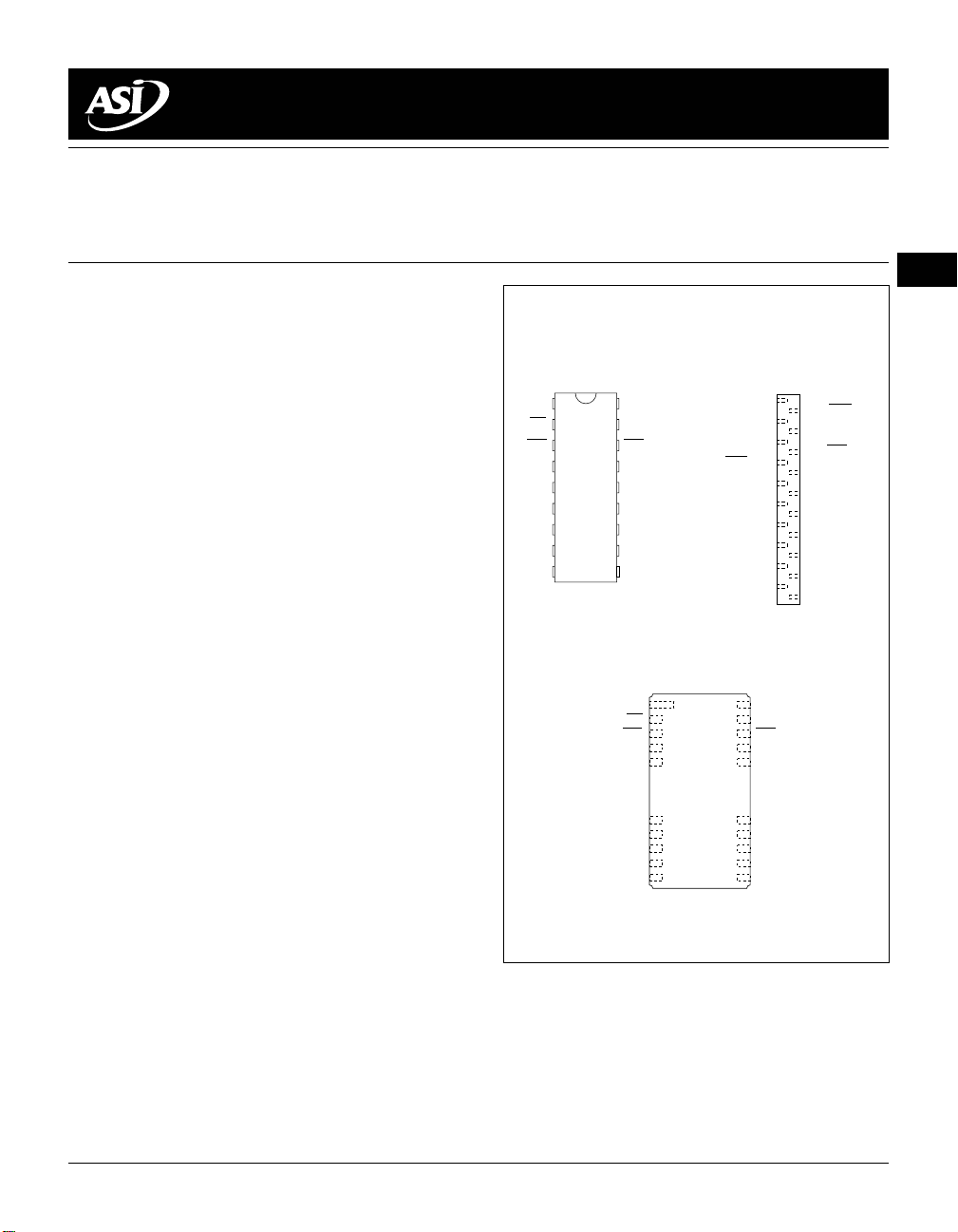
PIN ASSIGNMENT (Top View)
18-Pin DIP
1
D
2
WE
3
RAS
4
*A10
5
A0
6
A1
7
A2
8
A3
9
Vcc
18
Vss
17
Q
16
CAS
15
A9
14
A8
13
A7
12
A6
11
A5
10
A4
20-Pin SOJ
20-Pin LCC
20-Pin Gull Wing
1
D
2
WE
3
RAS
4
NC
5
*A10
20-Pin ZIP
A9
1
Q
3
D
5
RAS
7
NC
9
A0
11
A2
13
Vcc
15
A5
17
A7
19
26
Vss
25
Q
24
CAS
23
NC
22
A9
CAS
2
Vss
4
WE
6
A10*
8
NC
10
A1
12
A3
14
A4
16
A6
18
A8
20
• Packages
9
18
Ceramic DIP (300 mil) CN No. 101
Ceramic DIP (400 mil) C No. 102
Ceramic LCC ECN No. 202
Ceramic SOJ ECJ No. 504
Vcc
A0
10
A1
11
A2
12
A3
13
A8
17
A7
16
A6
15
A5
14
A4
Ceramic ZIP CZ No. 400
Ceramic Gull Wing ECG No. 600
*Address not used for /R/A//S-ONLY REFRESH
GENERAL DESCRIPTION
The MT4C1004J is a randomly accessed solid-state
memory containing 4,194,304 bits organized in a x1 configuration. During READ or WRITE cycles, each bit is uniquely
addressed through the 22 address bits which are entered 11
bits (A0-A10) at a time. /R/A/S is used to latch the first 11 bits
and /C/A/S the latter 11 bits. A READ or WRITE cycle is
selected with the ?W/E input. A logic HIGH on ?W/E dictates
READ mode while a logic LOW on ?W/E dictates WRITE
mode. During a WRITE cycle, data-in (D) is latched by the
MT4C1004J 883C Austin Semiconductor, Inc., reserves the right to change products or specifications without notice.
REV. 11/97
DS000021
falling edge of ?W/E or /C/A/S, whichever occurs last. If ?W/E
goes LOW prior to /C/?A/S going LOW, the output pin remains
open (High-Z) until the next /C/A/S cycle. If ?W/E goes LOW
after data reaches the output pin, Q is activated and retains
the selected cell data as long as /C/A/S remains LOW (regardless of ?W/E or /R/A/S). This LATE-?W/E pulse results in a
READ-WRITE cycle. FAST PAGE MODE operations allow
faster data operations (READ, WRITE or READ-MODIFYWRITE) within a row-address (A0 -A10) defined page
2-23
Page 2
AUSTIN SEMICONDUCTOR, INC.
AUSTIN SEMICONDUCTOR, INC.
MT5C1005 883C
MT4C1004J 883C
256K x 4 SRAM
4 MEG x 1 DRAM
boundary. The FAST PAGE MODE cycle is always initiated with a row address strobed-in by /R/A/S followed by a
column address strobed-in by /C/A/S. /C/A/S may be toggled-in
by holding /R/A/S
LOW and strobing-in different column
addresses, thus executing faster memory cycles. Returning
/R/A/S HIGH terminates the FAST PAGE MODE operation.
Returning /R//A/S and /C/A/S HIGH terminates a memory cycle
and decreases chip current to a reduced standby level. Also,
FUNCTIONAL BLOCK DIAGRAM
FAST PAGE MODE
WE
CAS
*EARLY-WRITE
DETECTION CIRCUIT
A10
NO. 2 CLOCK
GENERATOR
COLUMN
ADDRESS
11
11
BUFFER(11)
REFRESH
CONTROLLER
REFRESH
COUNTER
10
ROW
ADDRESS
BUFFERS (11)
A0
A1
A2
A3
A4
A5
A6
A7
A8
A9
the chip is preconditioned for the next cycle during the /R/A/
S HIGH time. Memory cell data is retained in its correct state
by maintaining power and executing any /R?A/S cycle (READ,
WRITE, /R?A/S-ONLY, /C/A/S-BEFORE-/R/A/S, or HIDDEN
FRESH) so that all 1,024 combinations
of /R?A/S addresses
(A0 -A9) are executed at least every 16ms, regardless of
sequence. The /C?A/S - BEFORE-/R?A/S cycle will
refresh counter for automatic /R/?A/S addressing.
DATA IN
BUFFER
DATA OUT
BUFFER
1024
DECODER
COLUMN
DECODER
4096
SENSE AMPLIFIERS
I/O GATING
4096
MEMORY
ARRAY
11
1
10
ROW
RE-
invoke the
D
Q
RAS
NO. 1 CLOCK
GENERATOR
Vcc
Vss
*NOTE: WE LOW prior to CAS LOW, EW detection circuit output is a HIGH (EARLY-WRITE)
CAS LOW prior to WE LOW, EW detection circuit output is a LOW (LATE-WRITE)
MT4C1004J 883C Austin Semiconductor, Inc., reserves the right to change products or specifications without notice.
REV. 11/97
DS000021
2-24
Page 3
MT5C1005 883C
AUSTIN SEMICONDUCTOR, INC.
AUSTIN SEMICONDUCTOR, INC.
MT4C1004J 883C
256K x 4 SRAM
4 MEG x 1 DRAM
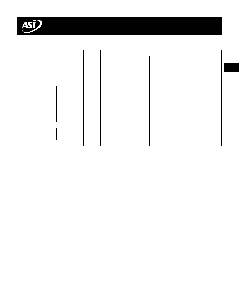
TRUTH TABLE
ADDRESSES DATA
FUNCTION ?R/A/S ?C/A/S ?W/E
Standby H H>X X X X Don’t Care High-Z
READ L L H ROW COL Don’t Care Data Out
EARLY-WRITE L L L ROW COL Data In High-Z
READ-WRITE L L H>L ROW COL Data In Data Out
FAST-PAGE-MODE 1st Cycle L H>L H ROW COL Don’t Care Data Out
READ 2nd Cycle L H>L H n/a COL Don’t Care Data Out
FAST-PAGE-MODE 1st Cycle L H>L L ROW COL Data In High-Z
EARLY-WRITE 2nd Cycle L H>L L n/a COL Data In High-Z
FAST-PAGE-MODE 1st Cycle L H>LH>L ROW COL Data In Data Out
READ-WRITE 2nd Cycle L H>LH>L n/a COL Data In Data Out
/R/A/S-ONLY REFRESH L H X ROW n/a Don’t Care High-Z
HIDDEN READ L>H>L L H ROW COL Don’t Care Data Out
REFRESH WRITE L>H>L L L ROW COL Data In High-Z
/C/A/S-BEFORE-/R/A/S REFRESH H>L L H X X Don’t Care High-Z
t
R
t
C D (Data In) Q (Data Out)
MT4C1004J 883C Austin Semiconductor, Inc., reserves the right to change products or specifications without notice.
REV. 11/97
DS000021
2-25
Page 4
AUSTIN SEMICONDUCTOR, INC.
AUSTIN SEMICONDUCTOR, INC.
MT5C1005 883C
MT4C1004J 883C
256K x 4 SRAM
4 MEG x 1 DRAM
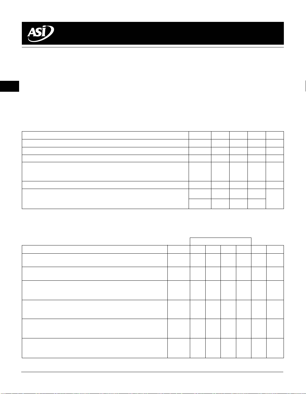
ABSOLUTE MAXIMUM RATINGS*
Voltage on any pin Relative to VSS ............... -1.0V to +7.0V
Power Dissipation ............................................................. 1W
Short Circuit Output Current ..................................... 50mA
Lead Temperature (Soldering 5 Seconds)................. 270°C
Storage Temperature................................... -65°C to +150°C
*Stresses greater than those listed under “Absolute Maximum Ratings” may cause permanent damage to the device.
This is a stress rating only and functional operation of the
device at these or any other conditions above those indicated in the operational sections of this specification is not
implied. Exposure to absolute maximum rating conditions
for extended periods may affect reliability.
ELECTRICAL CHARACTERISTICS AND RECOMMENDED DC OPERATING CONDITIONS
(Notes: 1, 6, 7) (-55°C ≤ TA ≤ 125°C; VCC = 5V ± 10%)
PARAMETER/CONDITION SYMBOL MIN MAX UNITS NOTES
Supply Voltage V
Input High (Logic 1) Voltage, All Inputs V
Input Low (Logic 0) Voltage, All Inputs V
INPUT LEAKAGE CURRENT
Any Input 0V ≤ VIN ≤ 5.5V VCC=5.5V II -5 5 µA
(All other pins not under test = 0V)
OUTPUT LEAKAGE CURRENT (Q is Disabled, 0V ≤ V
OUT ≤ 5.5V) VCC=5.5V IOZ -5 5 µA
OUTPUT LEVELS V
Output High Voltage (I
Output Low Voltage (I
OUT = -5mA)
OUT = 4.2mA) VOL 0.4 V
CC 4.5 5.5 V
IH 2.4 VCC+.5 V
IL -.5 0.8 V
OH 2.4 V
MAX
PARAMETER/CONDITION SYMBOL -7 -8 -10 -12 UNITS NOTES
STANDBY CURRENT (TTL) I
(/R/A/S = /C/A/S = V
IH)
STANDBY CURRENT (CMOS) I
(/R/A/S = /C/A/S = V
CC -0.2V; all other inputs = VCC -0.2V)
CC1 4444mA
CC2 2222mA
OPERATING CURRENT: Random READ/WRITE
Average Power-Supply Current I
(/R/A/S, /C/A/S, Address Cycling:
t
RC = tRC (MIN))
CC3 85 75 65 65 mA 3, 4
OPERATING CURRENT: FAST PAGE MODE
Average Power-Supply Current I
(/R/A/S = V
IL, /C/A/S, Address Cycling:
t
PC = tPC (MIN))
CC4 60 50 45 40 mA 3, 4
REFRESH CURRENT: /R/A/S-ONLY
Average Power-Supply Current I
(/R/A/S Cycling, /C/A/S = V
t
IH:
RC = tRC (MIN))
CC5 85 75 65 65 mA 3
REFRESH CURRENT: /C/A/S-BEFORE-/R/A/S
Average Power-Supply Current I
(/R/A/S, /C/A/S, Address Cycling:
MT4C1004J 883C Austin Semiconductor, Inc., reserves the right to change products or specifications without notice.
REV. 11/97
DS000021
t
RC = tRC (MIN))
2-26
CC6 85 75 65 65 mA 3, 5
Page 5
MT5C1005 883C
AUSTIN SEMICONDUCTOR, INC.
AUSTIN SEMICONDUCTOR, INC.
MT4C1004J 883C
256K x 4 SRAM
4 MEG x 1 DRAM
CAPACITANCE
PARAMETER SYMBOL MIN MAX UNITS NOTES
Input Capacitance: A0-A10, D C
Input Capacitance: /R/A/S, /C/A/S, ?W/EC
Output Capacitance: Q C
I1 7pF2
I27pF2
O 8pF2
ELECTRICAL CHARACTERISTICS AND RECOMMENDED AC OPERATING CONDITIONS
(Notes: 6, 7, 8, 9, 10, 11, 12, 13) (-55°C ≤ TC ≤ 125; VCC = 5V ± 10%)
AC CHARACTERISTICS -7 -8 -10 -12
PARAMETER SYM MIN MAX MIN MAX MIN MAX MIN MAX UNITS NOTES
Random READ or WRITE cycle time
READ-WRITE cycle time
FAST-PAGE-MODE READ
or WRITE cycle time
FAST-PAGE-MODE READ-WRITE
cycle time
Access time from /R/A/S
Access time from /C/A/S
Access time from column address
Access time from /C/A/S precharge
/R/A/S pulse width
/R/A/S pulse width (FAST PAGE MODE)
/R/A/S hold time
/R/A/S precharge time
/C/A/S pulse width
/C/A/S hold time
/C/A/S precharge time
/C/A/S precharge time (FAST PAGE MODE)
/R/A/S to /C/A/S delay time
/C/A/S to /R/A/S precharge time
Row address setup time
Row address hold time
/R/A/S to column
address delay time
Column address setup time
Column address hold time
Column address hold time
(referenced to /R/A/S)
Column address to
/R/A/S lead time
Read command setup time
Read command hold time
(referenced to /C/A/S)
Read command hold time
(referenced to /R/A/S)
/C/A/S to output in Low-Z
Output buffer turn-off delay
?W/E command setup time
t
RC 130 150 180 220 ns
t
RWC 155 175 210 255 ns
t
PC 40 45 55 70 ns
t
PRWC 65 70 85 140 ns
t
RAC 70 80 90 120 ns 14
t
CAC 20 20 25 30 ns 15
t
AA 35 40 45 60 ns
t
CPA 35 40 45 60 ns
t
RAS 70 10,000 80 10,000 100 10,000 120 100,000 ns
t
RASP 70 100,000 80 100,000 100 100,000 120 100,000 ns
t
RSH 20 20 25 30 ns
t
RP 50 60 70 90 ns
t
CAS 20 10,000 20 10,000 25 10,000 30 10,000 ns
t
CSH 70 80 100 120 ns
t
CPN 10 10 12 15 ns 16
t
CP 10 10 12 15 ns
t
RCD 20 50 20 60 25 75 25 90 ns 17
t
CRP 5 5 5 10 ns
t
ASR 0 0 0 0 ns
t
RAH 10 10 15 15 ns
t
RAD 15 35 15 40 20 50 20 60 ns 18
t
ASC 0 0 0 0 ns
t
CAH 15 20 25 25 ns
t
AR 50 60 70 85 ns
t
RAL 35 40 50 60 ns
t
RCS 0 0 0 0 ns
t
RCH 0 0 0 0 ns 19
t
RRH 0 0 0 0 ns 19
t
CLZ 0 0 0 0 ns
t
OFF0200 20 0 20020ns20
t
WCS 0 0 0 0 ns 21
MT4C1004J 883C Austin Semiconductor, Inc., reserves the right to change products or specifications without notice.
REV. 11/97
DS000021
2-27
Page 6

MT5C1005 883C
AUSTIN SEMICONDUCTOR, INC.
AUSTIN SEMICONDUCTOR, INC.
MT4C1004J 883C
256K x 4 SRAM
4 MEG x 1 DRAM
ELECTRICAL CHARACTERISTICS AND RECOMMENDED AC OPERATING CONDITIONS
(Notes: 6, 7, 8, 9, 10, 11, 12, 13) (-55°C ≤ TC ≤ 125; VCC = 5V ± 10%)
AC CHARACTERISTICS -7 -8 -10 -12
PARAMETER SYM MIN MAX MIN MAX MIN MAX MIN MAX UNITS NOTES
Write command hold time
Write command hold time
(referenced to /R/A/S)
Write command pulse width
Write command to /R/A/S lead time
Write command to /C/A/S lead time
Data-in setup time
Data-in hold time
Data-in hold time
(referenced to /R/A/S)
/R/A/S to ?W/E delay time
Column address
to ?W/E delay time
/C/A/S to ?W/E delay time
Transition time (rise or fall)
Refresh period (1,024 cycles)
/R/A/S to /C/A/S precharge time
/C/A/S setup time
(/C/A/S-BEFORE-/R/A/S REFRESH)
/C/A/S hold time
(/C/A/S-BEFORE-/R/A/S REFRESH)
?/W/E hold time
(/C/A/S-BEFORE-/R/A/S REFRESH)
?/W/E setup time
(/C/A/S-BEFORE-/R/A/S REFRESH)
?/W/E hold time
(WCBR test cycle)
?/W/E setup time
(WCBR test cycle)
t
WCH 15 15 20 25 ns
t
WCR 50 60 70 85 ns
t
WP 15 15 20 25 ns
t
RWL 20 20 25 30 ns
t
CWL 20 20 25 30 ns
t
DS 0 0 0 0 ns 22
t
DH 12 15 18 25 ns 22
t
DHR 50 60 70 90 ns
t
RWD 70 80 100 120 ns 21
t
AWD 35 40 50 60 ns 21
t
CWD 20 20 25 30 ns 21
t
T 350 350350 3 50ns
t
REF 16 16 16 16 ms
t
RPC 0 0 0 0 ns
t
CSR 10 10 10 10 ns 5
t
CHR 10 15 20 25 ns 5
t
WRH 10 10 10 10 ns 24, 25
t
WRP 10 10 10 10 ns 24, 25
t
WTH 10 10 10 10 ns 24, 25
t
WTS 10 10 10 10 ns 24, 25
MT4C1004J 883C Austin Semiconductor, Inc., reserves the right to change products or specifications without notice.
REV. 11/97
DS000021
2-28
Page 7

AUSTIN SEMICONDUCTOR, INC.
AUSTIN SEMICONDUCTOR, INC.
NOTES
1. All voltages referenced to VSS.
2. This parameter is sampled, not 100% tested.
Capacitance is measured with Vcc = 5V, f = 1 MHz at
less than 50mVrms, T
applied to each input and output individually with
remaining inputs and outputs open.
CC is dependent on cycle rates.
3. I
CC is dependent on output loading and cycle rates.
4. I
Specified values are obtained with minimum cycle
time and the output open.
5. Enables on-chip refresh and address counters.
6. The minimum specifications are used only to indicate
cycle time at which proper operation over the full
temperature range (-55°C ≤ T
7. An initial pause of 100µs is required after power-up
followed by eight /R?A/S refresh cycles (/R/A/S-ONLY or
CBR with ?/W/E HIGH) before proper device operation
is assured. The eight /R/A/S cycle wake-up should be
repeated any time the 16ms refresh requirement is
exceeded.
8. AC characteristics assume
IH (MIN) and VIL (MAX) are reference levels for
9. V
measuring timing of input signals. Transition times
are measured between V
and VIH).
10. In addition to meeting the transition rate specifica-
tion, all input signals must transit between V
IL (or between VIL and VIH) in a monotonic manner.
V
11. If /C/A/S = V
12. If /C/A/S = V
IH, data output is High-Z.
IL, data output may contain data from the
last valid READ cycle.
13. Measured with a load equivalent to 2 TTL gates and
100pF.
14. Assumes that
than the maximum recommended value shown in this
table,
exceeds the value shown.
15. Assumes that
t
t
RAC will increase by the amount that tRCD
t
16. If /C/A/S is LOW at the falling edge of /R/A/S, Q will be
maintained from the previous cycle. To initiate a new
= 25°C ±3°C, Vbias = 2.4V
A
≤ 125°C) is assured.
A
t
T = 5ns.
IH and VIL (or between VIL
IH and
RCD < tRCD (MAX). If tRCD is greater
RCD ≥ tRCD (MAX).
MT5C1005 883C
MT4C1004J 883C
256K x 4 SRAM
4 MEG x 1 DRAM
cycle and clear the data-out buffer, /C/A/S must be
pulsed HIGH for
17. Operation within the
t
RAC (MAX) can be met. tRCD (MAX) is specified as
a reference point only; if
specified
controlled exclusively by
18. Operation within the
t
RCD (MAX) can be met. tRAD (MAX) is specified as
a reference point only; if
specified
controlled exclusively by
t
19. Either
20.
RCH or tRRH must be satisfied for a READ
cycle.
t
OFF (MAX) defines the time at which the output
t
CPN.
t
RCD (MAX) limit ensures that
t
t
RCD (MAX) limit, then access time is
t
RAD (MAX) limit, then access time is
RCD is greater than the
t
CAC.
t
RAD (MAX) limit ensures that
t
RAD is greater than the
t
AA.
achieves the open circuit condition and is not
referenced to V
t
WCS, tRWD, tAWD and tCWD are restrictive
21.
operating parameters in LATE WRITE, READ-WRITE
and READ-MODIFY-WRITE cycles only. If
t
WCS (MIN), the cycle is an EARLY-WRITE cycle and
the data output will remain an open circuit throughout the entire cycle. If
t
AWD (MIN) and tCWD ≥ tCWD (MIN), the cycle is a
OH or VOL.
t
RWD ≥ tRWD (MIN), tAWD ≥
t
WCS ≥
READ-WRITE and the data output will contain data
read from the selected cell. If neither of the above
conditions are met, the cycle is a LATE-WRITE and
the state of Q is indeterminate (at access time and
until /C/A/S goes back to V
IH).
22. These parameters are referenced to /C/A/S leading edge
in EARLY-WRITE cycles and ?W/E leading edge in
LATE-WRITE or READ-WRITE cycles.
23. A HIDDEN REFRESH may also be performed after a
WRITE cycle. In this case ?W/E = LOW.
t
WTS and tWTH are set up and hold specifications for
24.
the ?W/E pin being held LOW to enable the JEDEC test
mode (with CBR timing constraints). These two
parameters are the inverts of
t
WRP and tWRH in the
CBR REFRESH cycle.
25. JEDEC test mode only.
MT4C1004J 883C Austin Semiconductor, Inc., reserves the right to change products or specifications without notice.
REV. 11/97
DS000021
2-29
Page 8

AUSTIN SEMICONDUCTOR, INC.
,
,,,
,,,
,,
,,,
,,
,
,
,,,
,,,
,
,,,
,
,,,
,,,
,,
AUSTIN SEMICONDUCTOR, INC.
READ CYCLE
t
RC
t
RAS
V
IH
V
RAS
IL
t
RCD
t
AR
t
ASC
COLUMN
t
RCS
CAS
ADDRVV
WE
Q
t
CRP
V
IH
V
IL
t
RAD
ROW
t
RAH
OPEN
t
ASR
IH
IL
V
IH
V
IL
V
OH
V
OL
EARLY-WRITE CYCLE
MT5C1005 883C
MT4C1004J 883C
256K x 4 SRAM
4 MEG x 1 DRAM
t
RP
t
CSH
t
RSH
t
CAS
t
RAL
t
CAH
t
AA
t
RAC
t
CAC
t
CLZ
VALID DATA
t
t
RRH
OFF
t
RCH
ROW
OPEN
MT4C1004J 883C Austin Semiconductor, Inc., reserves the right to change products or specifications without notice.
REV. 11/97
DS000021
V
IH
RAS
V
IL
V
IH
CAS
V
IL
V
IH
ADDR
V
IL
V
IH
WE
V
IL
V
IH
D
V
IL
V
OH
Q
V
OL
t
RC
t
RAS
t
CSH
t
COLUMNROW
VALID DATA
t
t
t
OPEN
RSH
CAS
RAL
CAH
t
t
t
t
t
t
t
CWL
RWL
WCR
WCH
WP
DHR
DH
t
CRP
t
RAD
t
ASR
t
RAH
t
WCS
t
RCD
t
AR
t
ASC
t
DS
t
RP
ROW
DON’T CARE
UNDEFINED
2-30
Page 9

AUSTIN SEMICONDUCTOR, INC.
,
,,
,,,,
,,,,
,,,
,,
,,,
,,,
,,,
,,,
,
,,
,,
,
,,
AUSTIN SEMICONDUCTOR, INC.
READ-WRITE CYCLE
(LATE-WRITE and READ-MODIFY-WRITE CYCLES)
t
RWC
t
RAS
V
IH
RAS
V
IL
t
RCD
t
t
t
RAD
RAH
t
t
t
t
AR
ASC
RWD
RCS
AWD
t
t
COLUMN ROW
t
CLZ
OPEN OPEN
CAS
ADDR
WE
t
CRP
V
IH
V
IL
t
ASR
V
IH
V
IL
V
IH
V
IL
V
IH
D
V
IL
V
OH
Q
V
OL
ROW
RAL
CAH
t
CWD
t
t
t
AA
RAC
CAC
t
CSH
t
RSH
t
CAS
t
DS
VALID DATA
t
CWL
t
RWL
t
WP
t
DH
VALID DATA
MT5C1005 883C
MT4C1004J 883C
256K x 4 SRAM
4 MEG x 1 DRAM
t
RP
t
OFF
RAS
CAS
ADDR
WE
Q
MT4C1004J 883C Austin Semiconductor, Inc., reserves the right to change products or specifications without notice.
REV. 11/97
DS000021
V
IH
V
IL
t
CRP
V
IH
V
IL
t
V
V
V
V
V
V
ASR
IH
IL
IH
IL
OH
OL
FAST-PAGE-MODE READ CYCLE
t
RASP
RCH
VALID
DATA
t
PC
t
CP
t
t
CAH
ASC
t
t
OFF
t
CLZ
t
CSH
t
RCD
t
t
RAD
t
RAH
AR
t
ASC
t
RCS
t
CAS
t
CAH
t
t
AA
t
RAC
t
CAC
t
CLZ
2-31
RCS
t
t
t
t
AA
CPA
CAC
t
RP
t
RSH
t
CP
CAS
t
RCH
t
OFF
VALID
DATA
t
CAS
t
RAL
t
t
CAH
ASC
COLUMNCOLUMNCOLUMNROW ROW
t
RCS
t
AA
t
CPA
t
CAC
t
CLZ
VALID
DATA
t
CPN
t
RRH
t
RCH
t
OFF
OPENOPEN
DON’T CARE
UNDEFINED
Page 10

AUSTIN SEMICONDUCTOR, INC.
,,
,,
,,,,
,,
,
,,
,,,
,
,
,
,,
,,,
,,
AUSTIN SEMICONDUCTOR, INC.
FAST-PAGE-MODE EARLY-WRITE CYCLE
MT5C1005 883C
MT4C1004J 883C
256K x 4 SRAM
4 MEG x 1 DRAM
V
IH
RAS
V
CAS
ADDR
IL
t
CRP
V
IH
V
IL
t
ASR
V
IH
V
IL
V
IH
WE
V
IL
V
IH
D
V
IL
V
IH
Q
V
IL
t
CSH
t
RCD
t
t
RAD
t
RAH
AR
t
ASC
t
WCS
t
DS
FAST-PAGE-MODE READ-WRITE CYCLE
(LATE-WRITE and READ-MODIFY-WRITE CYCLES)
V
IH
RAS
V
IL
t
CRP
V
IH
CAS
V
IL
t
ASRtRAH
V
IH
ADDR
V
IL
V
IH
WE
V
IL
V
IH
D
V
IL
V
OH
Q
V
OL
*tPC = LATE-WRITE Cycle
t
PRWC = FAST READ-MODIFY-WRITE Cycle
ROW COLUMN COLUMN COLUMN ROW
t
CSH
t
RCD
t
t
RAD
AR
t
ASC
t
RWD
t
RCS
t
AWD
t
CWD
t
CLZ
OPEN OPEN
t
RASP
t
PC
VALID
DATA
t
CP
t
RASP
t
PC
*
t
CP
t
ASCtCAH
t
t
CWD
t
CLZ
t
CAS
t
CAH
t
CWL
t
WCH
t
WP
t
WCR
t
DHR
t
DH
VALID DATA VALID DATA VALID DATA
t
CAS
t
CAH
t
CWL
t
WP
tDHt
DS
VALID DATA
t
AA
t
RAC
t
CACtOFF
t
ASC
t
WCS
t
DStDH
OPEN
t
PRWC
AWD
DS
VALID DATA
t
CAS
t
CAH
t
CWL
t
WCH
t
WP
t
CAS
t
CWL
t
WP
tDHt
t
AA
t
CPA
t
CACtOFF
VALID
DATA
t
CP
t
ASC
COLUMNCOLUMNCOLUMNROW ROW
t
WCS
t
DStDH
t
t
ASC
t
CWD
CLZ
AWD
t
CAH
DS
VALID DATA
t
AA
t
CPA
t
CAC
RSH
t
CAS
t
t
t
tDHt
t
CP
t
t
RWL
CWL
WP
t
RP
t
RSH
t
CAS
t
RAL
t
CAH
t
CWL
t
WCH
t
WP
t
RWL
t
RAL
VALID
DATA
t
CPN
t
RP
t
CPN
t
OFF
DON’T CARE
UNDEFINED
MT4C1004J 883C Austin Semiconductor, Inc., reserves the right to change products or specifications without notice.
REV. 11/97
DS000021
2-32
Page 11

AUSTIN SEMICONDUCTOR, INC.
,
,,,
,,,
,,,
,,
,,,
,,,,
,
,,
,,,
,
,,
AUSTIN SEMICONDUCTOR, INC.
//
//
//
/R
/A
/S-ONLY REFRESH CYCLE
//
//
//
RAS
CAS
ADDR
(ADDR = A0-A9; A10
V
IH
V
IL
V
IH
V
IL
V
IH
V
IL
V
OH
Q
V
OL
t
CRP
t
ASR
ROW
//
//
//
/C
/A
/S-BEFORE-
//
//
//
t
RAH
and ?W/E = DON’T CARE)
t
t
RAS
//
//
//
/R
/A
/S REFRESH CYCLE
//
//
//
RC
OPEN
(A0-A10 = DON’T CARE)
MT5C1005 883C
MT4C1004J 883C
256K x 4 SRAM
4 MEG x 1 DRAM
t
RP
t
RPC
ROW
RAS
CAS
Q
WE
ADDR
t
V
IH
V
IL
V
IH
V
IL
V
IH
V
IL
t
RPC
t
CPN
RP
t
CSR
t
WRPtWRH
t
t
RAS
CHR
t
RPC
OPEN
t
RP
HIDDEN REFRESH CYCLE
t
CSR
t
WRPtWRH
t
CHR
23
t
RAS
(?W/E = HIGH)
(READ) (REFRESH)
t
RAS
V
IH
RAS
V
IL
t
CRP
V
IH
CAS
V
IL
t
ASR
V
IH
V
IL
V
OH
Q
V
OL
t
RCD
t
AR
t
RAD
t
RAH
t
t
t
ASC
COLUMNROW
t
t
t
t
RAL
CAH
AA
RAC
CAC
CLZ
t
RP
t
RSH
t
RAS
t
CHR
t
OFF
OPENVALID DATAOPEN
DON’T CARE
UNDEFINED
MT4C1004J 883C Austin Semiconductor, Inc., reserves the right to change products or specifications without notice.
REV. 11/97
DS000021
2-33
Page 12

AUSTIN SEMICONDUCTOR, INC.
,,,
,
,,,
,,,
,,,
,,
,,,,
,,,
,,,
,,,
AUSTIN SEMICONDUCTOR, INC.
MT5C1005 883C
MT4C1004J 883C
256K x 4 SRAM
4 MEG x 1 DRAM
4 MEG POWER-UP AND REFRESH
CONSTRAINTS
The EIA/JEDEC 4 Meg DRAM introduces two potential
incompatibilities compared to the previous generation
1 Meg DRAM. The incompatibilities involve refresh and
power-up. Understanding these incompatibilities and providing for them will offer the designer and system user
greater compatibility between the 1 Meg and 4 Meg.
REFRESH
The most commonly used refresh mode of the 1 Meg is
the CBR (?C?A/S-BEFORE-?R?A/S) REFRESH cycle. The CBR for
the 1 Meg specifies the ?W/E pin as a “don’t care.” The 4 Meg,
on the other hand, specifies the CBR REFRESH mode with
the ?W/E pin held at a voltage HIGH level.
A CBR cycle with ?W/E LOW will put the 4 Meg into the
JEDEC specified test mode (WCBR).
WCBR TEST MODE: WE
4 MEG
DRAM
V
IH
RAS
V
IL
V
IH
CAS
V
IL
V
OH
Q
V
OL
CBR REFRESH: WE
t
RP
t
RPC
t
t
CPN
CSR
t
WTStWTH
V
IH
V
IL
t
WRPtWRH
V
IH
V
IL
t
CHR
t
RAS
POWER-UP
The 4 Meg JEDEC test mode constraint may introduce
another problem. The 1 Meg POWER-UP cycle requires a
100µs delay followed by any eight ?R?A/S cycles. The 4 Meg
POWER-UP is more restrictive in that eight ?R?A/S-ONLY or
CBR REFRESH (?W/E held HIGH) cycles must be used. The
restriction is needed since the 4 Meg may power-up in the
JEDEC specified test mode and must exit out of the test
mode. The only way to exit the 4 Meg JEDEC test mode is
with either a ?R?A/S-ONLY or a CBR REFRESH cycle (?W/E
held HIGH).
SUMMARY
1. The 1 Meg CBR REFRESH allows the ?W/E pin to be
“don’t care” while the 4 Meg CBR requires ?W/E to be
HIGH.
2. The eight ?R?A/S wake-up cycles on the 1 Meg may be any
valid ?R?A/S cycle while the 4 Meg may only use ?R?A/SONLY or CBR REFRESH cycles (?W/E held HIGH).
OPEN
t
RPC
t
RP
t
CSR
t
WTS
t
WRPtWRH
t
CHR
t
WTH
t
RAS
1 MEG
DRAM
MT4C1004J 883C Austin Semiconductor, Inc., reserves the right to change products or specifications without notice.
REV. 11/97
DS000021
CBR REFRESH: WE
V
IH
V
IL
COMPARISON OF 4 MEG TEST MODE AND WCBR TO 1 MEG CBR
2-34
DON’T CARE
Page 13

AUSTIN SEMICONDUCTOR, INC.
AUSTIN SEMICONDUCTOR, INC.
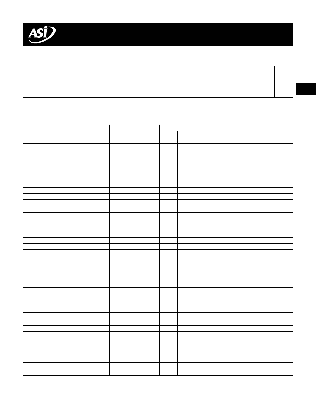
ELECTRICAL TEST REQUIREMENTS
MT5C1005 883C
MT4C1004J 883C
256K x 4 SRAM
4 MEG x 1 DRAM
MIL-STD-883 TEST REQUIREMENTS (per Method 5005, Table I)
INTERIM ELECTRICAL (PRE-BURN-IN) TEST PARAMETERS 2, 8A, 10
(Method 5004)
FINAL ELECTRICAL TEST PARAMETERS 1*, 2, 3, 7*, 8, 9, 10, 11
(Method 5004)
GROUP A TEST REQUIREMENTS 1, 2, 3, 4**, 7, 8, 9, 10, 11
(Method 5005)
GROUP C AND D END-POINT ELECTRICAL PARAMETERS 1, 2, 3, 7, 8, 9, 10, 11
(Method 5005)
* PDA applies to subgroups 1 and 7.
** Subgroup 4 shall be measured only for initial qualification and after process or design changes, which may affect input
or output capacitance.
SUBGROUPS
MT4C1004J 883C Austin Semiconductor, Inc., reserves the right to change products or specifications without notice.
REV. 11/97
DS000021
2-35
Page 14

AUSTIN SEMICONDUCTOR, INC.
AUSTIN SEMICONDUCTOR, INC.
MT5C1005 883C
MT4C1004J 883C
256K x 4 SRAM
4 MEG x 1 DRAM
MT4C1004J 883C Austin Semiconductor, Inc., reserves the right to change products or specifications without notice.
REV. 11/97
DS000021
2-36
 Loading...