

Page 1
1
128Mb: x8DDR400 SDRAM Micron Technology, Inc., reserves the right to change products or specifications without notice.
128Mbx8DDR400.p65 – Rev. A (1/30/02-B) ©2002, Micron Technology, Inc.
128Mb: x8
DDR400 SDRAM Addendum
‡
THIS DATA SHEET CONTAINS THE PRESENT DESCRIPTION OF A PRODUCT IN DEFINITION WITH NO FORMAL DESIGN IN PROGRESS.
PREVIEW
‡
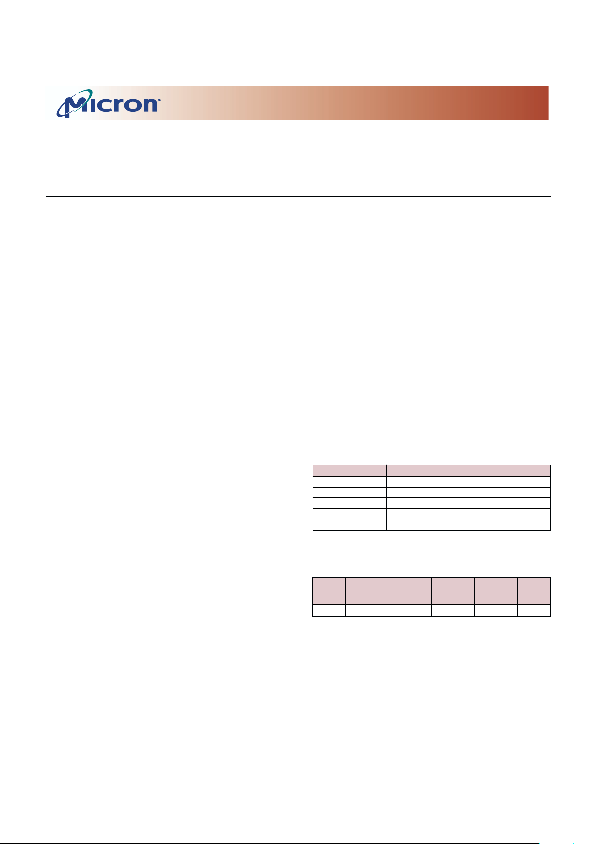
KEY TIMING PARAMETERS
SPEED CLOCK RATE DATA-OUT ACCESS DQS-DQ
GRADE CL = 3
1
WINDOW2WINDOW SKEW
-5 200 MHz 2.15ns ±0.50ns +0.35ns
NOTE: 1. CL = CAS (Read) Latency
2. With a 50/50 clock duty cycle
Architecture 16 Meg x 8
Configuration 4 Meg x 8 x 4 banks
Refresh Count 4K
Row Addressing 4K (A0–A11)
Bank Addressing 4 (BA0, BA1)
Column Addressing 1K (A0–A9)
DOUBLE DATA RATE
(DDR) SDRAM
MT46V16M8 – 4 Meg x 8 x 4 banks
For the latest data sheet revisions, please refer to the Micron
Web site: www.micron.com/dramds
FEATURES
• 200 MHz Clock, 400 Mb/s/p data rate
•VDD = +2.65V ±0.10V
•VDDQ = +2.65V ±0.10V
• Bidirectional data strobe (DQS) transmitted/
received with data, i.e., source-synchronous data
capture
• Internal, pipelined double-data-rate (DDR)
architecture; two data accesses per clock cycle
• Differential clock inputs (CK and CK#)
• Commands entered on each positive CK edge
• DQS edge-aligned with data for READs; centeraligned with data for WRITEs
• DLL to align DQ and DQS transitions with CK
• Four internal banks for concurrent operation
• Data mask (DM) for masking write data
• Programmable burst lengths: 2, 4, or 8
• Concurrent Auto Precharge option supported
• Auto Refresh and Self Refresh Modes
•tRAS lockout (tRAP = tRCD)
OPTIONS PART NUMBER
• Configuration
16 Meg x 8 (4 Meg x 8 x 4 banks) 16M8
• Plastic Package
66-Pin TSOP TG
(400mil with 0.65mm pin pitch)
• Timing - Cycle Time
5ns @ CL = 3
(1)
-5
• Self Refresh
Standard none
NOTE: 1. Supports modules with 3-4-4 timing
CONFIGURATION
GENERAL DESCRIPTION
The DDR400 SDRAM is a high-speed CMOS, dynamic random-access memory that operates at a frequency of 200 MHz (
t
CK=5ns) with a peak data transfer
rate of 400Mb/s. DDR400 continues to use the JEDEC
standard SSTL_2 interface and the 2n-prefetch architecture.
The standard DDR200/DDR266 data sheets also
pertain to the DDR400 device and should be referenced for a complete description of DDR SDRAM functionality and operating modes. However, to meet the
faster DDR400 operating frequencies, some of the AC
timing parameters, DC levels and operating temperatures are slightly tighter. This addendum data sheet
will concentrate on the key differences required to support the enhanced speeds.
The Micron 128Mb data sheet provides full specifications and functionality unless specified herein.
Page 2
2
128Mb: x8DDR400 SDRAM Micron Technology, Inc., reserves the right to change products or specifications without notice.
128Mbx8DDR400.p65 – Rev. A (1/30/02-B) ©2002, Micron Technology, Inc.
128Mb: x8
DDR400 SDRAM Addendum
PREVIEW
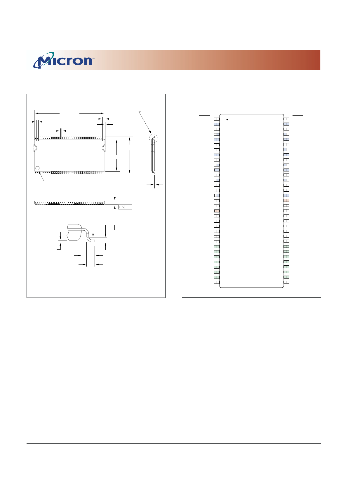
66-PIN TSOP PACKAGE PIN ASSIGNMENT
66-PIN TSOP PACKAGE DIMENSION
SEE DETAIL A
0.10
0.65 TYP
0.71
10.16 ±0.08
0.15
0.50 ±0.10
PIN #1 ID
DETAIL A
22.22 ± 0.08
0.32 ± .075 TYP
+0.03
-0.02
+0.10
-0.05
1.20 MAX
0.10
0.25
11.76 ±0.10
0.80 TYP
0.10 (2X)
GAGE PLANE
(TOP VIEW)
NOTE: 1. All dimensions in millimeters.
2. Package width and length do not include mold protrusion; allowable mold protrusion is 0.25mm
per side.
1
2
3
4
5
6
7
8
9
10
11
12
13
14
15
16
17
18
19
20
21
22
23
24
25
26
27
28
29
30
31
32
33
66
65
64
63
62
61
60
59
58
57
56
55
54
53
52
51
50
49
48
47
46
45
44
43
42
41
40
39
38
37
36
35
34
V
SS
DQ7
V
SS
Q
NC
DQ6
V
DD
Q
NC
DQ5
V
SS
Q
NC
DQ4
V
DD
Q
NC
NC
V
SS
Q
DQS
DNU
V
REF
V
SS
DM
CK#
CK
CKE
NC
NC
A11
A9
A8
A7
A6
A5
A4
V
SS
x8
V
DD
DQ0
V
DD
Q
NC
DQ1
V
SS
Q
NC
DQ2
V
DD
Q
NC
DQ3
V
SS
Q
NC
NC
V
DD
Q
NC
NC
V
DD
DNU
NC
WE#
CAS#
RAS#
CS#
NC
BA0
BA1
A10/AP
A0
A1
A2
A3
V
DD
x8
Page 3
3
128Mb: x8DDR400 SDRAM Micron Technology, Inc., reserves the right to change products or specifications without notice.
128Mbx8DDR400.p65 – Rev. A (1/30/02-B) ©2002, Micron Technology, Inc.
128Mb: x8
DDR400 SDRAM Addendum
PREVIEW
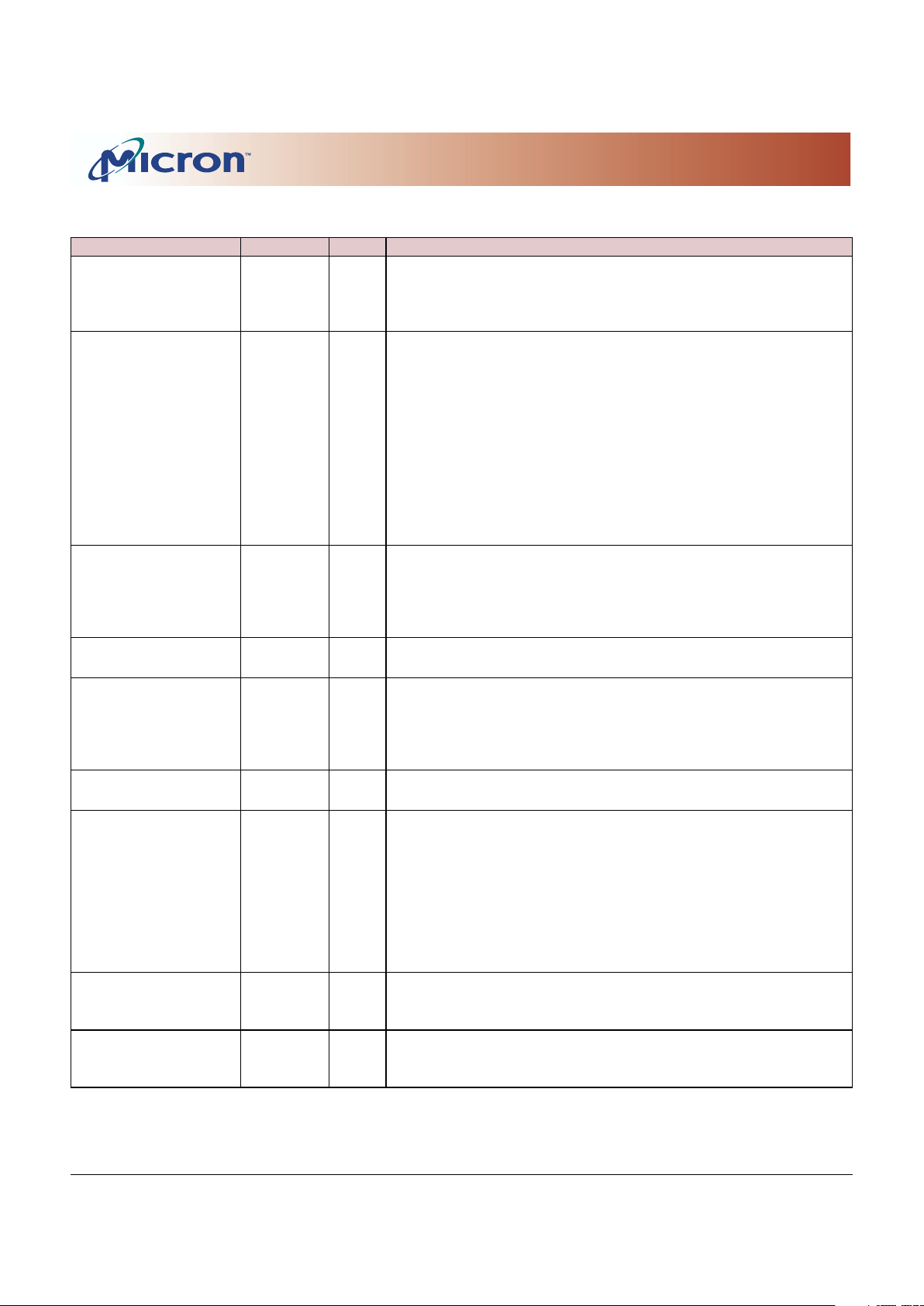
PIN DESCRIPTIONS
PIN NUMBERS SYMBOL TYPE DESCRIPTION
45, 46 CK, CK# Input Clock: CK and CK# are differential clock inputs. All address and
control input signals are sampled on the crossing of the positive
edge of CK and negative edge of CK#. Output data (DQs and
DQS) is referenced to the crossings of CK and CK#.
44 CKE Input Clock Enable: CKE HIGH activates and CKE LOW deactivates the
internal clock, input buffers and output drivers. Taking CKE LOW
provides PRECHARGE POWER-DOWN and SELF REFRESH
operations (all banks idle), or ACTIVE POWER-DOWN (row
ACTIVE in any bank). CKE is synchronous for POWER-DOWN
entry and exit, and for SELF REFRESH entry. CKE is asynchronous
for SELF REFRESH exit and for disabling the outputs. CKE must be
maintained HIGH throughout read and write accesses. Input
buffers (excluding CK, CK#, and CKE) are disabled during
POWER-DOWN. Input buffers (excluding CKE) are disabled
during SELF REFRESH. CKE is an SSTL_2 input but will detect an
LVCMOS LOW level after VDD is applied.
24 CS# Input Chip Select: CS# enables (registered LOW) and disables (regis-
tered HIGH) the command decoder. All commands are masked
when CS# is registered HIGH. CS# provides for external bank
selection on systems with multiple banks. CS# is considered part
of the command code.
23, 22, 21 RAS#, CAS#, Input Command Inputs: RAS#, CAS#, and WE# (along with CS#) define the
WE# command being entered.
47 DM Input Input Data Mask: DM is an input mask signal for write data. Input
data is masked when DM is sampled HIGH along with that input
data during a WRITE access. DM is sampled on both edges of
DQS. Although DM pins are input-only, the DM loading is
designed to match that of DQ and DQS pins.
26, 27 BA0, BA1 Input Bank Address Inputs: BA0 and BA1 define to which bank an
ACTIVE, READ, WRITE, or PRECHARGE command is being applied.
29-32 A0, A1, A2 Input Address Inputs: Provide the row address for ACTIVE commands, and
32, 35, 36 A3, A4, A5 the column address and auto precharge bit (A10) for READ/WRITE
36, 38, 39 A6, A7, A8 commands, to select one location out of the memory array in the
40, 29, 41 A9, A10, A11 respective bank. A10 sampled during a PRECHARGE command
determines whether the PRECHARGE applies to one bank (A10 LOW,
bank selected by BA0, BA1) or all banks (A10 HIGH). The address inputs
also provide the op-code during a MODE REGISTER SET command. BA0
and BA1 define which mode register (mode register or extended mode
register) is loaded during the LOAD MODE REGISTER command.
2, 5, 8 DQ0-2 I/O Data Input/Output.
11, 56, 59 DQ3-5
62, 65 DQ6-7
51 DQS I/O Data Strobe: Output with read data, input with write data. DQS is
edge-aligned with read data, centered in write data. It is used to
capture data.
(continued on next page)
Page 4
4
128Mb: x8DDR400 SDRAM Micron Technology, Inc., reserves the right to change products or specifications without notice.
128Mbx8DDR400.p65 – Rev. A (1/30/02-B) ©2002, Micron Technology, Inc.
128Mb: x8
DDR400 SDRAM Addendum
PREVIEW
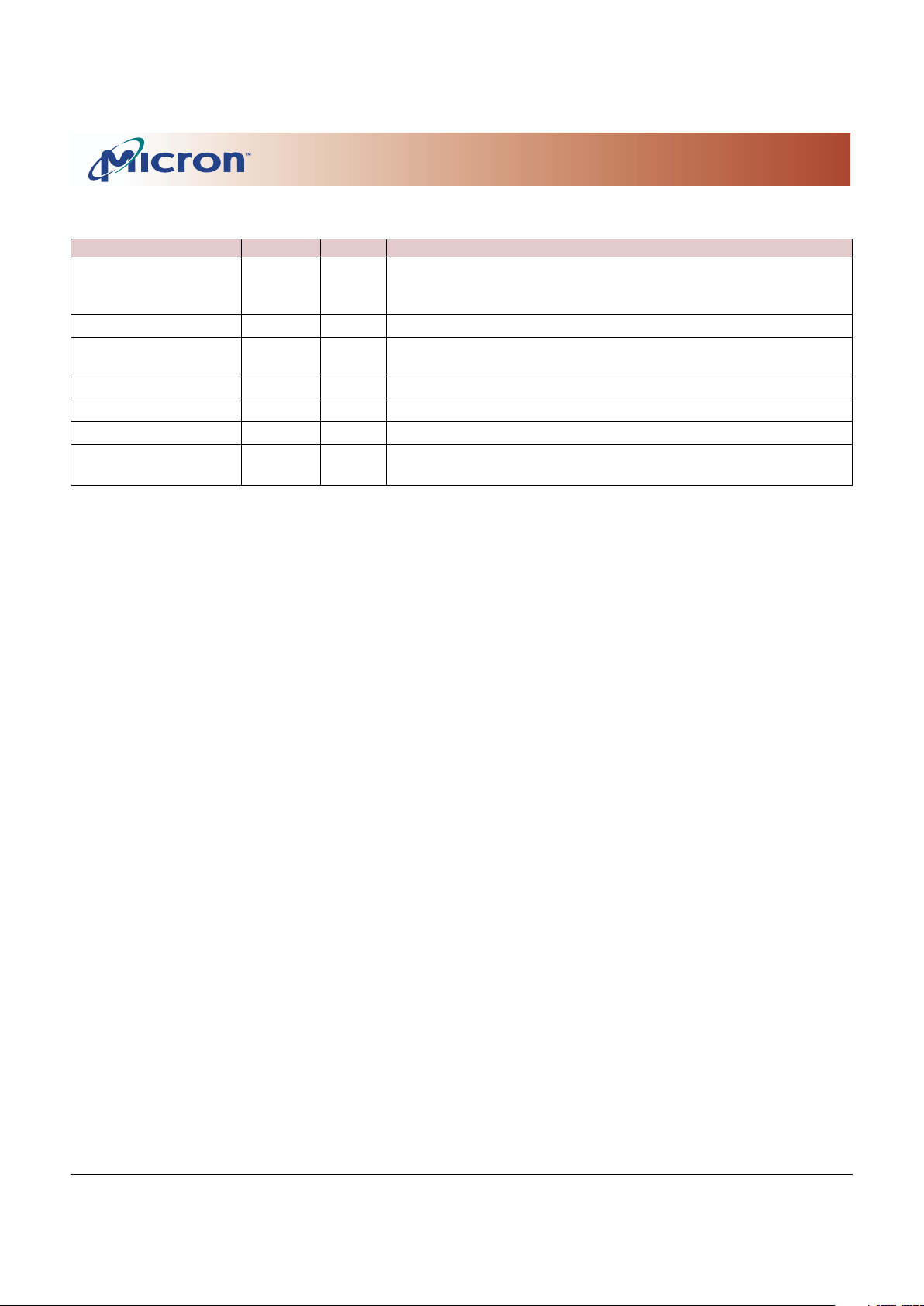
PIN DESCRIPTIONS (continued)
PIN NUMBERS SYMBOL TYPE DESCRIPTION
4, 7, 10, 13, 14,
16, 17,
20, NC -
No Connect: These pins should be left unconnected.
20, 25,
42, 43, 53,
54, 57,
60,
63
19, 50 DNU – Do Not Use: Must float to minimize noise on Vref
3, 9, 15, 55, VDDQ Supply DQ Power Supply: +2.65V ±0.10V. Isolated on the die for
61 improved noise immunity.
6, 12, 52, 58, 64 VSSQ Supply DQ Ground. Isolated on the die for improved noise immunity.
1, 18, 33 VDD Supply Power Supply: +2.65V ±0.10V.
4, 48, 66 VSS Supply Ground.
49 VREF Supply SSTL_2 reference voltage.
Page 5
5
128Mb: x8DDR400 SDRAM Micron Technology, Inc., reserves the right to change products or specifications without notice.
128Mbx8DDR400.p65 – Rev. A (1/30/02-B) ©2002, Micron Technology, Inc.
128Mb: x8
DDR400 SDRAM Addendum
PREVIEW
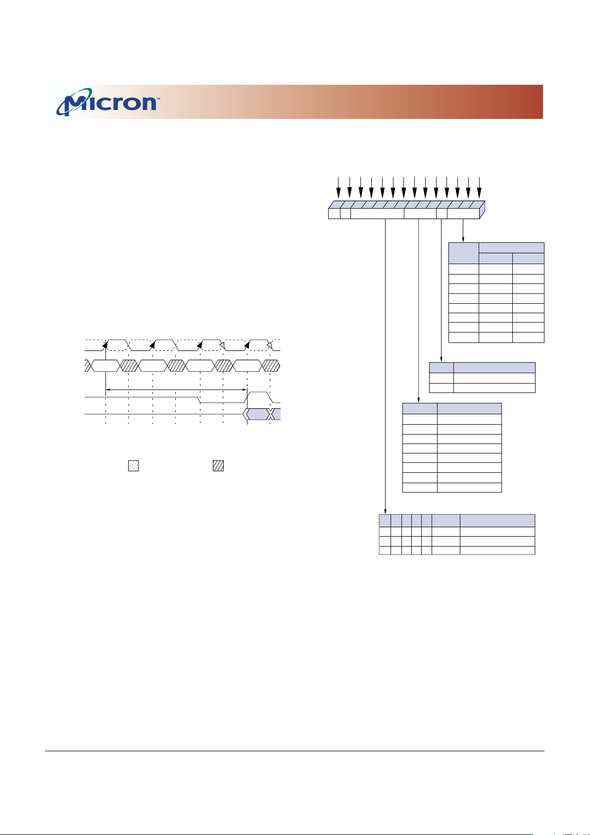
READ LATENCY
The READ latency is the delay, in clock cycles,
between the registration of a READ command and the
availability of the first bit of output data. The latency
should be set to 3 clocks, as shown in the CAS Latency
Diagram and Mode Register Definition Diagram.
If a READ command is registered at clock edge n,
and the latency is m clocks, the data will be available
nominally coincident with clock edge n + m.
Reserved states should not be used as unknown
operation or incompatibility with future versions may
result.
CK
CK#
COMMAND
DQ
DQS
CL = 3
READ NOP NOP NOP
Burst Length = 4 in the cases shown
Shown with nominal tAC and nominal tDSDQ
T0 T1 T2 T2n T3 T3n
DON’T CARETRANSITIONING DATA
CAS Latency
Diagram
Mode Register Definition
Diagram
M3 = 0
Reserved
2
4
8
Reserved
Reserved
Reserved
Reserved
M3 = 1
Reserved
2
4
8
Reserved
Reserved
Reserved
Reserved
Operating Mode
Normal Operation
Normal Operation/Reset DLL
All other states reserved
0
1
-
0
0
-
0
0
-
0
0
-
0
0
-
Valid
Valid
-
0
1
Burst Type
Sequential
Interleaved
CAS Latency
Reserved
Reserved
Reserved
3
Reserved
Reserved
Reserved
Reserved
Burst Length
M0
0
1
0
1
0
1
0
1
Burst LengthCAS Latency BT0*
A9 A7 A6 A5 A4 A3A8 A2 A1 A0
Mode Register (Mx)
Address Bus
9765438210
M1
0
0
1
1
0
0
1
1
M2
0
0
0
0
1
1
1
1
M3
M4
0
1
0
1
0
1
0
1
M5
0
0
1
1
0
0
1
1
M6
0
0
0
0
1
1
1
1
M6-M0
M8
M7
Operating Mode
A10BA0 A11BA1
10111213
0*
* M13 and M12 (BA0 and BA1)
must be “0, 0” to select the
base mode register (vs. the
extended mode register).
M9M10M11
Page 6
6
128Mb: x8DDR400 SDRAM Micron Technology, Inc., reserves the right to change products or specifications without notice.
128Mbx8DDR400.p65 – Rev. A (1/30/02-B) ©2002, Micron Technology, Inc.
128Mb: x8
DDR400 SDRAM Addendum
PREVIEW
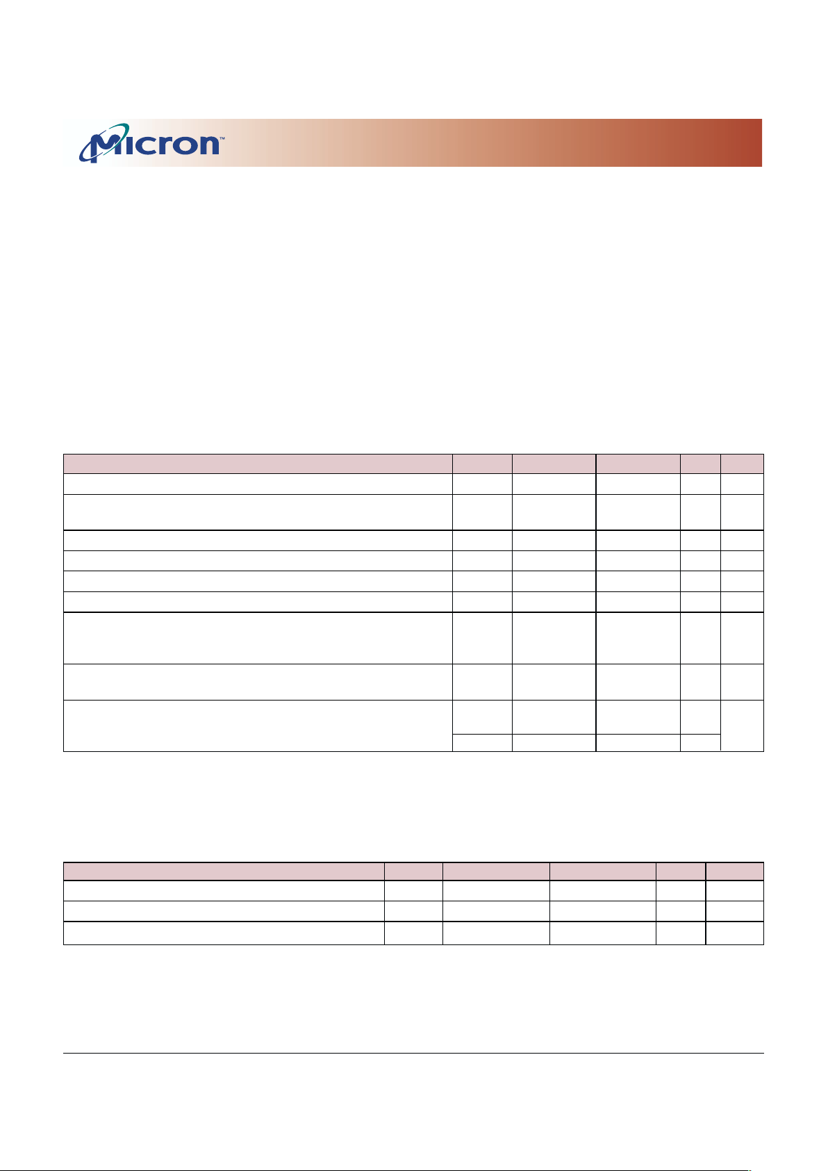
DC ELECTRICAL CHARACTERISTICS AND OPERATING CONDITIONS
(Notes: 1–5, 16; refer to DDR200/266 data sheet for all notes)
(0°C ≤ TA ≤ +50°C; VDD = +2.65V ±0.10V, VDDQ = +2.65V ±0.10V)
PARAMETER/CONDITION SYMBOL MIN MAX UNITS NOTES
Supply Voltage VDD 2.55 2.75 V 36, 41
I/O Supply Voltage VDDQ 2.55 2.75 V 36, 41,
44
I/O Reference Voltage VREF 0.49 x VDDQ 0.51 x VDDQ V 6, 44
I/O Termination Voltage (system) VTT VREF - 0.04 VREF + 0.04 V 7, 44
Input High (Logic 1) Voltage VIH(DC)VREF + 0.15 VDD + 0.3 V 28
Input Low (Logic 0) Voltage VIL(DC) -0.3 VREF - 0.15 V 28
INPUT LEAKAGE CURRENT
Any input 0V ≤ VIN ≤ VDD, VREF pin 0V ≤ VIN ≤ 1.35V II -2 2 µA
(All other pins not under test = 0V)
OUTPUT LEAKAGE CURRENT IOZ -5 5 µA
(DQs are disabled; 0V ≤ VOUT ≤ VDDQ)
OUTPUT LEVELS: Full drive option - x8
High Current (VOUT = VDDQ-0.373V, minimum VREF, minimum VTT)IOH -16.8 – mA 37, 39
Low Current (VOUT = 0.373V, maximum VREF, maximum VTT)IOL 16.8 – mA
AC INPUT OPERATING CONDITIONS
(Notes: 1–5, 16; refer to DDR200/266 data sheet for all notes)
(0°C ≤ TA ≤ +50°C; VDD = +2.65V ±0.10V, VDDQ = +2.65V ±0.10V)
PARAMETER/CONDITION SYMBOL MIN MAX UNITS NOTES
Input High (Logic 1) Voltage VIH(AC)VREF + 0.310 – V 14, 28, 40
Input Low (Logic 0) Voltage VIL(AC) – VREF - 0.310 V 14, 28, 40
I/O Reference Voltage VREF(AC) 0.49 x VDDQ 0.51 x VDDQV 6
ABSOLUTE MAXIMUM RATINGS*
VDD Supply Voltage Relative to VSS ....... -1V to +3.6V
V
DDQ Supply Voltage Relative to VSS .... -1V to +3.6V
V
REF and Inputs Voltage Relative to VSS .. -1V to +3.6V
I/O Pins Voltage Relative to VSS . -0.5V to VDDQ +0.5V
Operating Temperature, T
A
(ambient) .. 0°C to +50°C
Storage Temperature (plastic) .......... -55°C to +150°C
Power Dissipation .................................................. 1W
Short Circuit Output Current ........................... 50mA
*Stresses greater than those listed under “Absolute
Maximum Ratings” may cause permanent damage to
the device. This is a stress rating only, and functional
operation of the device at these or any other conditions
above those indicated in the operational sections of
this specification is not implied. Exposure to absolute
maximum rating conditions for extended periods may
affect reliability.
Page 7
7
128Mb: x8DDR400 SDRAM Micron Technology, Inc., reserves the right to change products or specifications without notice.
128Mbx8DDR400.p65 – Rev. A (1/30/02-B) ©2002, Micron Technology, Inc.
128Mb: x8
DDR400 SDRAM Addendum
PREVIEW
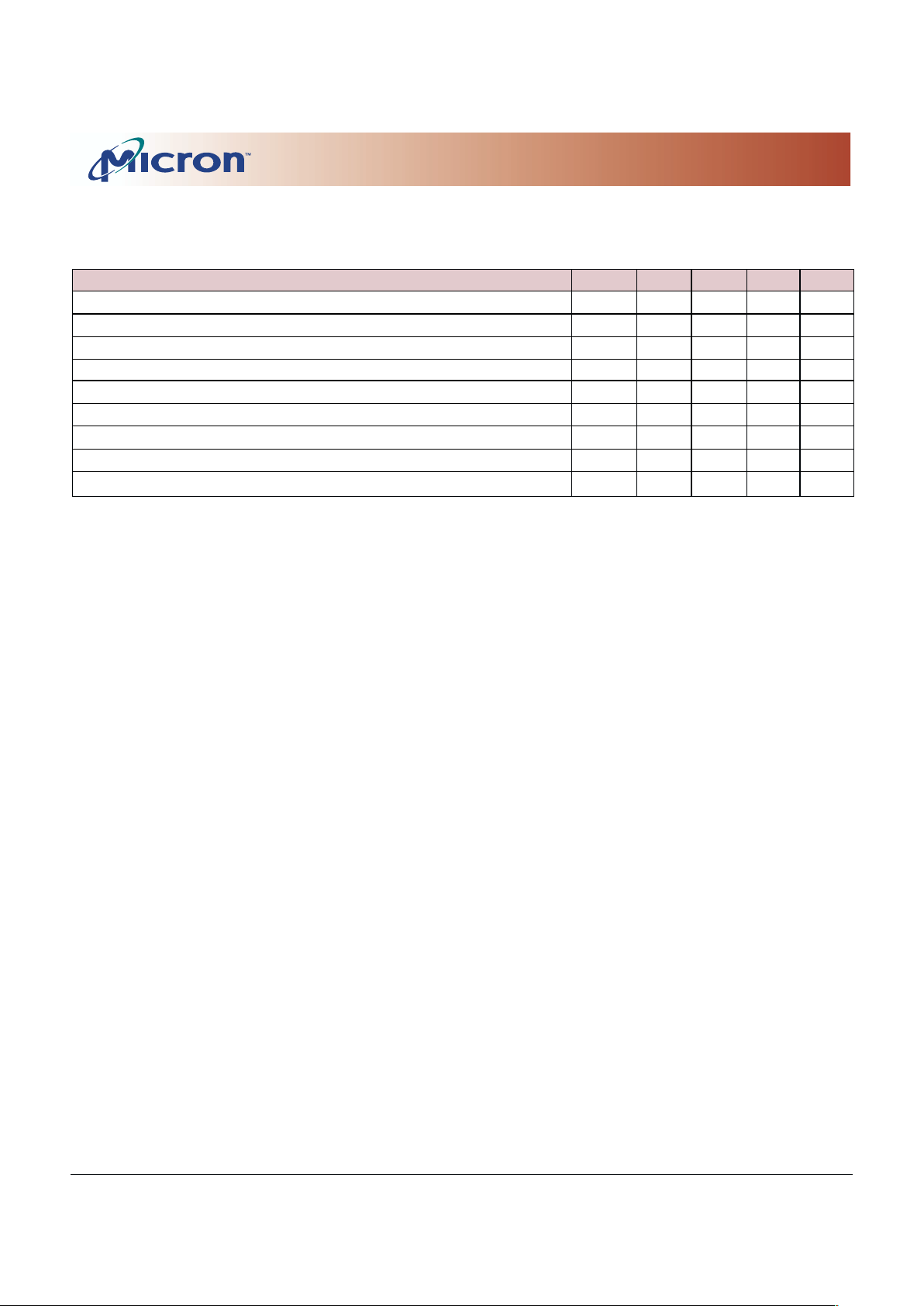
CAPACITANCE (TSOP)
(Notes: 1-5, 14-17, 33; refer to DDR200/266 data sheet for all notes)
(0°C ≤ TA ≤ 70°C; VDDQ = +2.65V ±0.10V, VDD = +2.65V ±0.10V)
PARAMETER SYMBOL MIN MAX UNITS NOTES
Delta Input/Output Capacitance:
DQs, DQS, DM DCIO – 0.50 pF 13, 24
DQ0-DQ7 DCIO – 0.50 pF 13, 24
Delta Input Capacitance: Command and Address DCI1 – 0.50 pF 13, 29
Delta Input Capacitance: CK, CK# DCI2 – 0.25 p F 13, 29
Input/Output Capacitance: DQs, DQS, DM CIO 4.0 5.0 pF 13
Input Capacitance: Command and Address CI1 2.0 3.0 p F 13
Input Capacitance: CK, CK# CI2 2.0 3.0 p F 13
Input Capacitance: CKE C
I3 2.0 3.0 p F 13
Page 8
8
128Mb: x8DDR400 SDRAM Micron Technology, Inc., reserves the right to change products or specifications without notice.
128Mbx8DDR400.p65 – Rev. A (1/30/02-B) ©2002, Micron Technology, Inc.
128Mb: x8
DDR400 SDRAM Addendum
PREVIEW
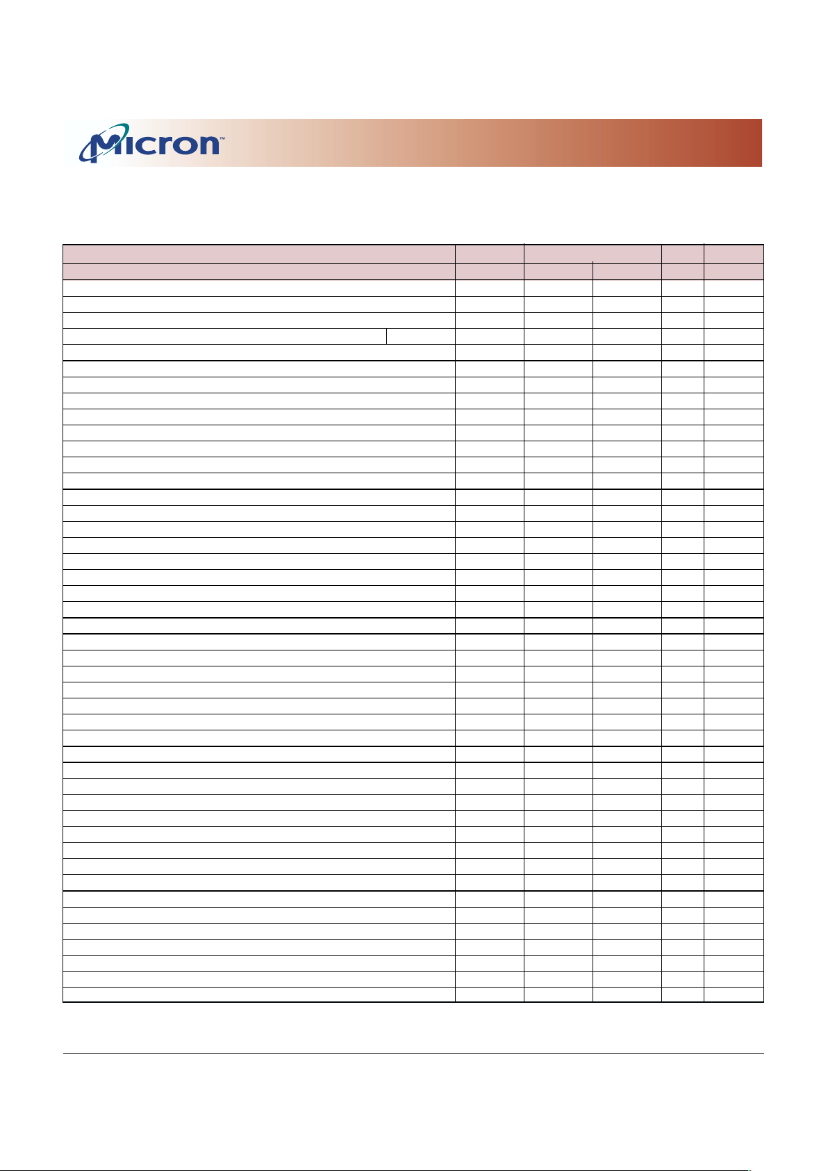
AC CHARACTERISTICS -5 (TSOP)
PARAMETER SYMBOL MIN MAX UNITS NOTES
Access window of DQs from CK/CK#
t
AC -0.6 +0.6 ns
CK high-level width
t
CH 0.45 0.55
t
CK 30
CK low-level width
t
CL 0.45 0.55
Clock cycle time CL = 3
t
CK 5 5 ns 45,52
DQ and DM input hold time relative to DQS
t
DH 0.45 na ns 26,31
DQ and DM input setup time relative to DQS
t
DS 0.45 ns 26,31
DQ and DM input pulse width (for each input)
t
DIPW 1.4 ns 31
Access window of DQS from CK/CK#
t
DQSCK -0.50 +0.50 ns
DQS input high pulse width
t
DQSH 0.4
t
CK
DQS input low pulse width
t
DQSL 0.4
t
CK
DQS-DQ skew, DQS to last DQ valid, per group, per access
t
DQSQ 0.35 ns 25, 26
Write command to first DQS latching transition
t
DQSS 0.75 1.25
t
CK
DQS falling edge to CK rising - setup time
t
DSS 0.22
t
CK
DQS falling edge from CK rising - hold time
t
DSH 0.22
t
CK
Half clock period
t
HP
t
CH,tCL ns 34
Data-out high-impedance window from CK/CK#
t
HZ +0.60 ns 18,42
Data-out low-impedance window from CK/CK#
t
LZ -0.60 ns 18,43
Address and control input hold time (fast slew rate)
t
IH
F
0.75 ns 14
Address and control input setup time (fast slew rate)
t
IS
F
0.75 ns 14
Address and control input hold time (slow slew rate)
t
IH
S
na n s 14
Address and control input setup time (slow slew rate)
t
IS
S
na n s 14
Address and control input pulse width
t
IPW 1.8 ns
LOAD MODE REGISTER command cycle time
t
MRD 10 ns
DQ-DQS hold, DQS to first DQ to go non-valid, per access
t
QH
t
HP
-
t
QHS ns 25, 26
Data Hold Skew Factor
t
QHS 0.50 ns
ACTIVE to AUTOPRECHARGE command
t
RAP 20 ns 46
ACTIVE to PRECHARGE command
t
RAS 40 70,000 ns 35
ACTIVE to ACTIVE/AUTO REFRESH command period
t
RC 60 ns
AUTO REFRESH command period
t
RFC 70 ns 50
ACTIVE to READ or WRITE delay
t
RCD 20 n s
PRECHARGE command period
t
RP 20 ns
DQS read preamble
t
RPRE 0.9 1.1
t
CK 42
DQS read postamble
t
RPST 0.4 0.6
t
CK
ACTIVE bank a to ACTIVE bank b command
t
RRD 10 n s
DQS write preamble
t
WPRE 0.25
t
CK
DQS write preamble setup time
t
WPRES 0 ns 20, 21
DQS write postamble
t
WPST 0.4 0.6
t
CK 19
Write recovery time
t
WR 15 ns
Internal WRITE to READ command delay
t
WTR 2
t
CK
Data valid output window na
t
QH - tDQSQ ns 25
REFRESH to REFRESH command interval
t
REFC 140.6 µs 23
Average periodic refresh interval
t
REFI 15.6 µs 23
Terminating voltage delay to VDD
t
VTD 0 ns
Exit SELF REFRESH to non-READ command
t
XSNR 75 ns
Exit SELF REFRESH to READ command
t
XSRD 200
t
CK
ELECTRICAL CHARACTERISTICS AND RECOMMENDED AC OPERATING CONDITIONS
(Notes: 1-5, 14-17, 33; refer to DDR200/266 data sheet for all notes)
(0°C ≤ TA ≤ 50°C; VDDQ = +2.65V ±0.10V, VDD = +2.65V ±0.10V)
Page 9

9
128Mb: x8DDR400 SDRAM Micron Technology, Inc., reserves the right to change products or specifications without notice.
128Mbx8DDR400.p65 – Rev. A (1/30/02-B) ©2002, Micron Technology, Inc.
128Mb: x8
DDR400 SDRAM Addendum
PREVIEW
8000 S. Federal Way, P.O. Box 6, Boise, ID 83707-0006, Tel: 208-368-3900
E-mail: [email protected], Internet: http://www.micron.com, Customer Comment Line: 800-932-4992
Micron is a registered trademark and the Micron logo and M logo are trademarks of Micron Technology, Inc.
 Loading...