

Page 1
MT3608
AEROSEMI
FEATURES
• Integrated 80mΩ Power MOSFET
• 2V to 24V Input Voltage
• 1.2MHz Fixed Switching Frequency
• Internal 4A Switch Current Limit
• Adjustable Output Voltage
• Internal Compensation
• Up to 28V Output Voltage
• Automatic Pulse Frequency Modulation
Mode at Light Loads
• up to 97% Efficiency
• Available in a 6-Pin SOT23-6 Package
APPLICATIONS
• Battery-Powered Equipment
• Set-Top Boxed
• LCD Bais Supply
• DSL and Cable Modems and Routers
• Networking cards powered from PCI
or PCI express slots
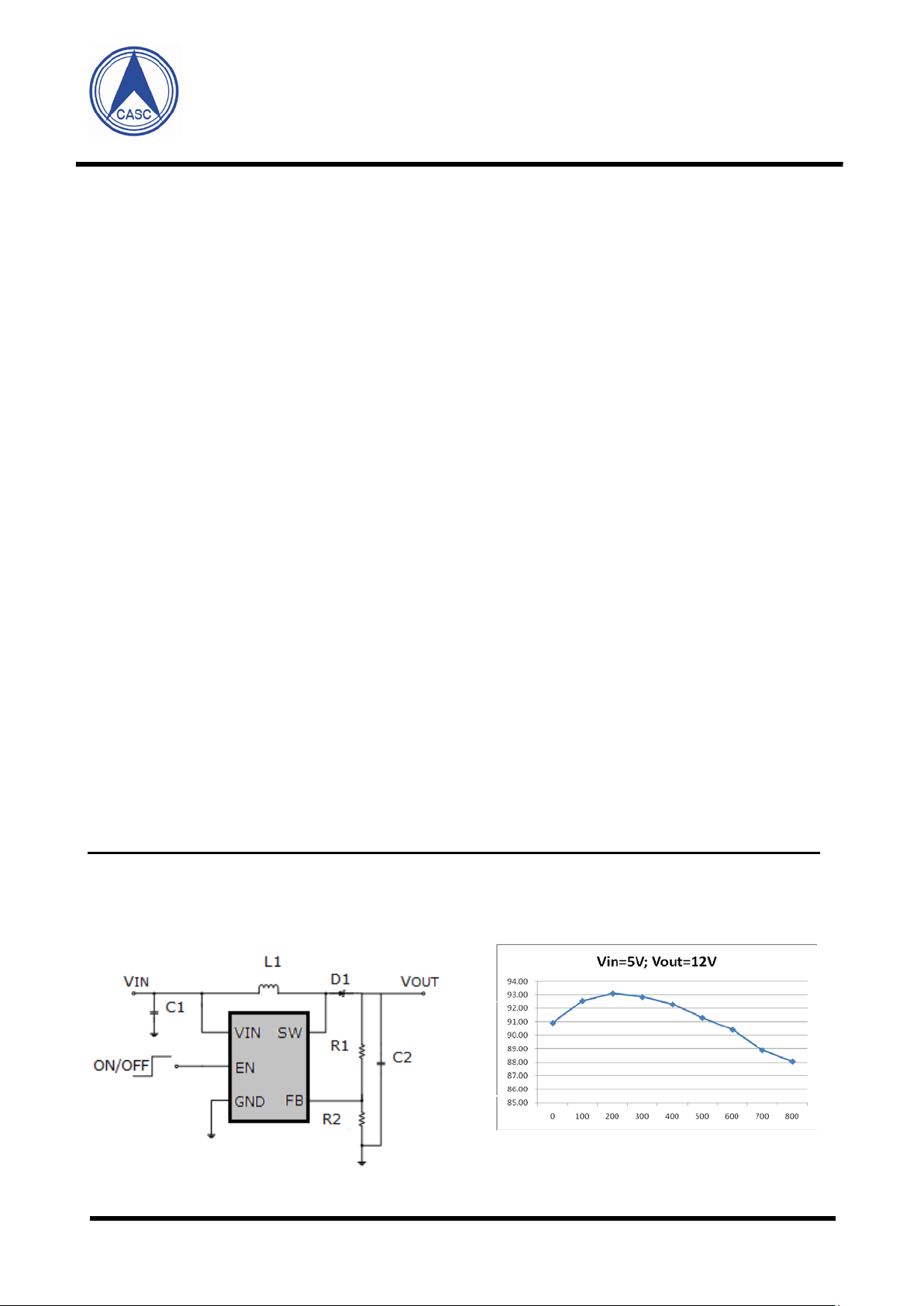
TYPICAL APPLICATION
High Efficiency 1.2MHz
2A Step Up Converter
GENERAL DESCRIPTION
The MT3608 is a constant frequency, 6-pin SOT23
current mode step-up converter intended for small,
low power applications. The MT3608 switches at
1.2MHz and allows the use of tiny, low cost
capacitors and inductors 2mm or less in height.
Internal soft-start results in small inrush current and
extends battery life.
The MT3608 features automatic shifting to pulse
frequency modulation mode at light loads. The
MT3608 includes under-voltage lockout, current
limiting, and thermal overload protection to prevent
damage in the event of an output overload. The
MT3608 is available in a small 6-pin SOT-23
package.
Efficiency
Figure 1. Basic Application Circuit
Aerosemi Technology Co., Ltd
1
Efficiency (%)
Iout (mA)
Figure 2. Efficiency Curve
Page 2
MT3608
Aerosemi Technology Co., Ltd
3
1
2
4
6
SOT23-5
IN
GND
FB
SW
EN
(MT3540)
5
NC
Power Switch Output. SW is the drain of the internal MOSFET switch. Connect the
Regulator On/Off Control Input. A high input at EN turns on the converter , and a
Input Supply Pin. Must be locally bypassed.
6
NC
NC
SOT23-6
ABSOLUTE MAXIMUM RATINGS
IN, EN voltages ………..….…… -0.3V to 26V
Operating Temperature….... -40°C to +85°C
FB Voltages ................................-0.3V to 6V
Junction Temperature ………………...160°C
SW Voltage ……………………..-0.3V to 30V
Storage Temperature Range -65°C to 150°C
Peak SW Sink and Source Curr ent ………4A
Lead Temperature (Soldering, 10s) ...+300°C
PACKAGE/ORDER INFORMATION
(MT3608)
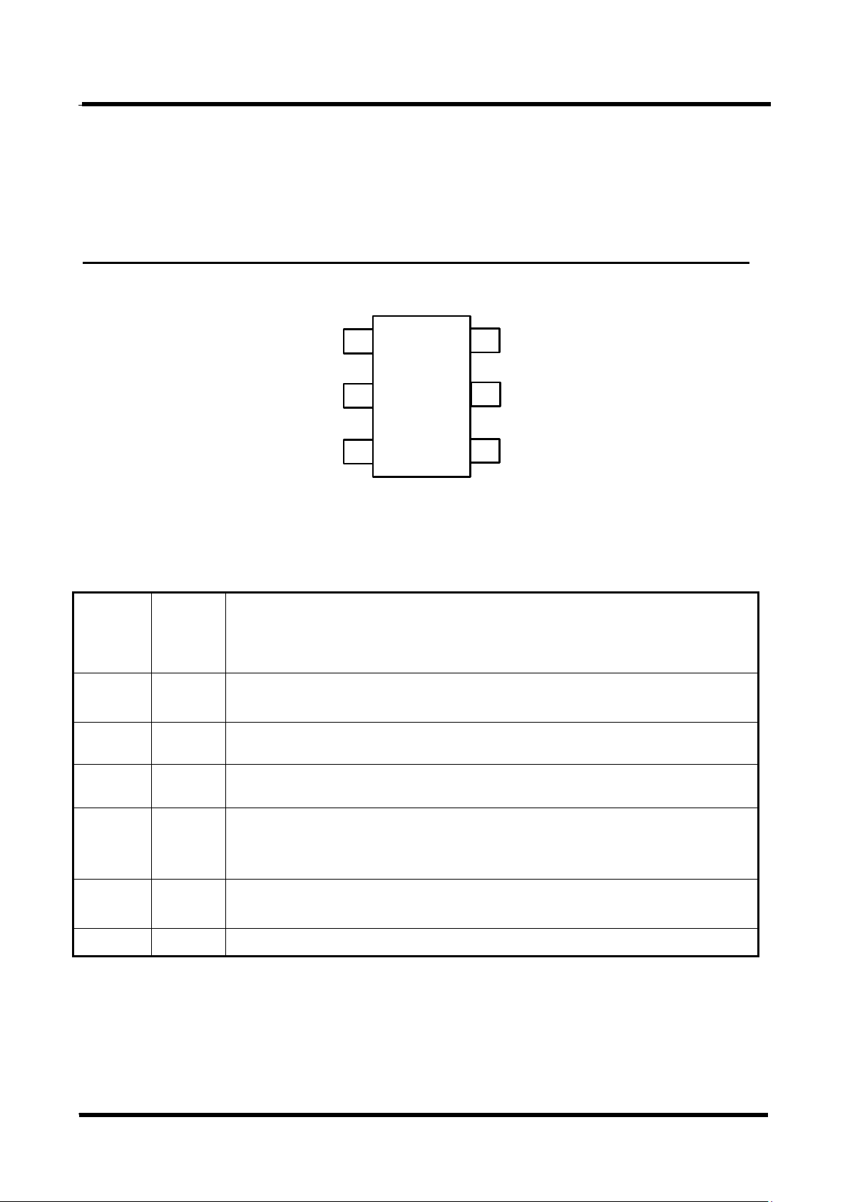
PIN DESCRIPTION
PIN
1 SW
2 GND Ground Pin
3 FB Feedback Input. The FB voltage is 0.6V. Connect a resistor divider to FB.
4 EN
5 IN
NAME FUNCTION
power inductor and output rectifier to SW. SW can swing between GND and 28V.
low input turns it off. When not used, connect EN to the input supply for automatic
startup.
2
Page 3

MT3608
Aerosemi Technology Co., Ltd
ELECTRICAL CHARACTERISTICS
(VIN=VEN=5V, TA = 25°C, unless otherwise noted.)
Parameter Conditions MIN TYP MAX unit
Operating Input Voltage 2 24 V
Under Voltage Lockout 1.98 V
Under Voltage Lockout Hysteresis 100 mV
Current (Shutdown) VEN= 0V 0.1 1 µA
Quiescent Current (PFM)
Quiescent Current (PWM)
VFB=0.7V,No switch
VFB=0.5V,switch
100 200 µA
1.6 2.2 mA
Switching Frequency 1.2 MHz
Maximum Duty Cycle VFB = 0V 90 %
EN Input High Voltage 1.5 V
EN Input Low Voltage 0.4 V
FB Voltage 0.588 0.6 0.612 V
FB Input Bias Current VFB = 0.6V -50 -10 nA
SW On Resistance (1) 80 150 mΩ
SW Current Limit (1) VIN= 5V, Duty cycle=50% 4 A
SW Leakage VSW = 20V 1 μA
Thermal Shutdown 155
℃
Note:
1) Guaranteed by design, not tested.
3
Page 4
MT3608
Aerosemi Technology Co., Ltd
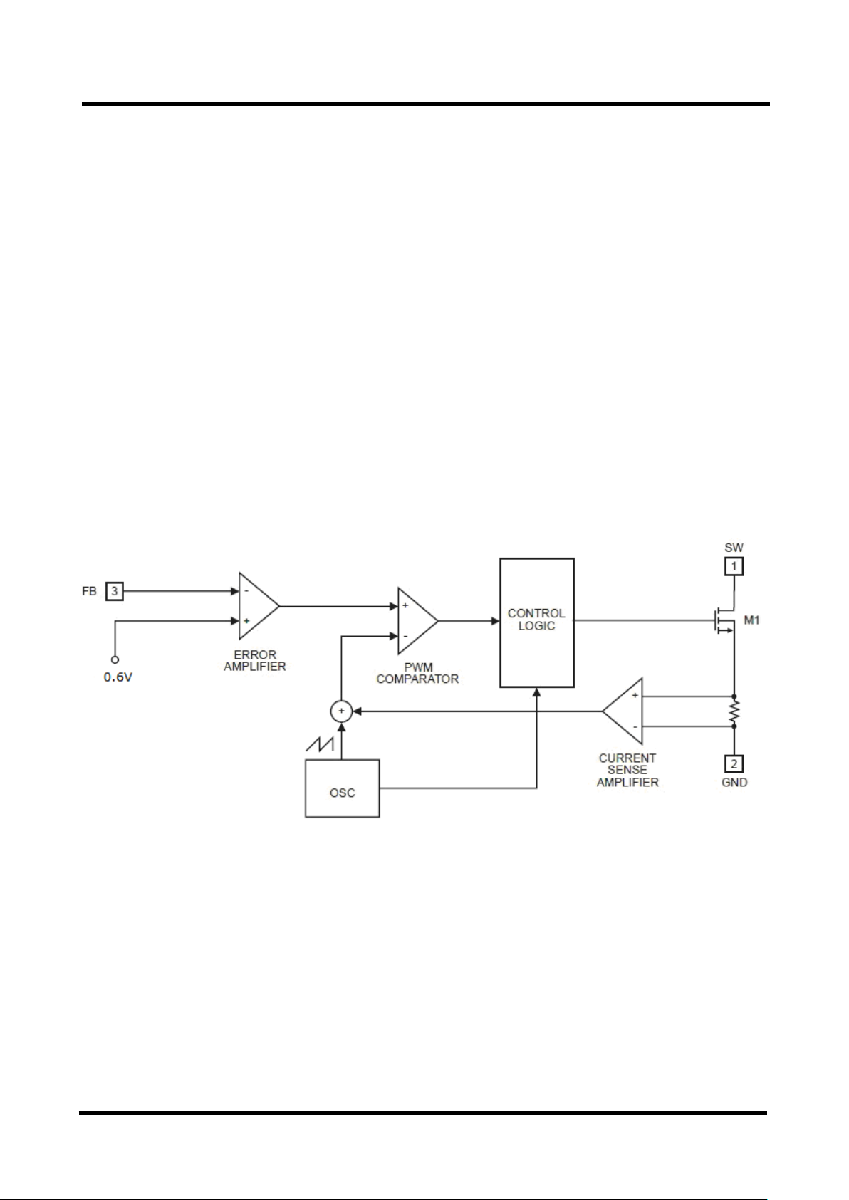
OPERATION
The MT3608 uses a fixed frequency, peak current
mode boost regulator architecture to regulate
voltage at the feedback pin. The operation of the
MT3608 can be understood by referring to the block
diagram of Figure 3. At the start of each oscillator
cycle the MOSFET is turned on through the control
circuitry. To prevent sub-harmonic oscillations at
duty cycles greater than 50 percent, a stabilizing
ramp is added to the output of the current sense
amplifier and the result is fed into the negative input
of the PWM comparator. When this voltage equals
The output voltage of the error amplifier the power
MOSFET is turned off. The voltage at the output of
the error amplifier is an amplified version of the
difference between the 0.6V bandgap reference
voltage and the feedback voltage. In this way the
peak current level keeps the output in regulation. If
the feedback voltage starts to drop, the output of the
error amplifier increases. These results in more
current to flow through the power MOSFET, thus
increasing the power delivered to the output. The
MT3608 has internal soft start to limit the amount of
input current at startup and to also limit the amount
of overshoot on the output.
Figure 3. Functional Block D iagr am
4
Page 5
MT3608
Aerosemi Technology Co., Ltd
Vout(V)
Vout(V)
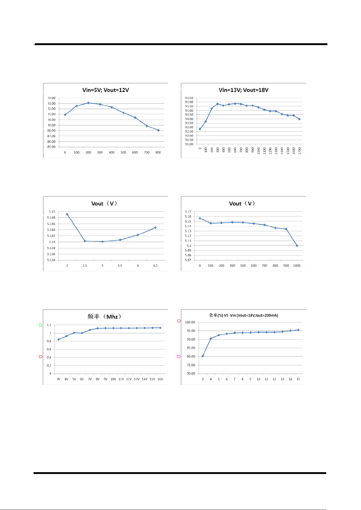
TYPICAL OPERATING CHARACTERISTICS
Efficiency Curve
Efficiency
Iout (mA)
line Regulation
Efficiency Curve
Current limit(A)
Iout(mA)
Load regualation
Vin (V)
Freq VS Vin
Iout (mA)
Efficiency VS Vin
5
Page 6

MT3608
Aerosemi Technology Co., Ltd
)1(
2
1
R
R
VV
REFOUT
+×=
PEAKOUTD
IIRMSI ×≈)(
APPLICATION INFORMATION
Setting the Output Voltage
The internal reference VREF is 0.6V (Typical).The
output voltage is divided by a resistor divider,R1 and
R2 to the FB pin. The output voltage is given by
Inductor Selection
The recommended values of inductor are 4.7 to
22μH. Small size and better efficiency are the major
concerns for portable device, such as MT3608 used
for mobile phone. The inductor should have low core
loss at 1.2MHz and low DCR for better efficiency. To
avoid inductor saturation current rating should be
considered.
Capacitor Selection
Input and output ceramic capacitors of 22μF are
recommended for MT3608 applications. For better
voltage filtering, ceramic capacitors with low ESR
are recommended. X5R and X7R types are suitable
because of their wider voltage and temperature
ranges.
Diode Selection
Schottky diode is a good choice for MT3608
because of its low forward voltage drop and fast
reverses recovery. Using Schottky diode can get
better efficiency. The high speed rectification is also
a good characteristic of Schottky diode for high
switching frequency. Current rating of the diode must
meet the root mean square of the peak current and
output average current multiplication as following :
Layout Consideration
For best performance of the MT3608, the following
guidelines must be strictly followed.
Input and Output capacitors should be placed
close to the IC and connected to ground plane
to reduce noise coupling.
The GND should be connected to a strong
ground plane for heat sinking and noise
protection.
Keep the main current traces as possible as
short and wide.
SW node of DC-DC converter is with high
frequency voltage swing. It should be kept at a
small area.
Place the feedback components as close as
possible to the IC and keep away from the
noisy devices.
The diode’ s reverse breakdown voltage should be
larger than the output voltage.
6
Page 7
MT3608
Aerosemi Technology Co., Ltd
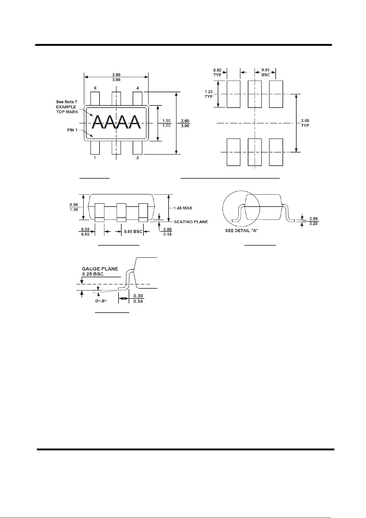
PACKAGE DESCRIPTION
Xi' an Aerosemi Technol ogy Co., Ltd
TOP VIEW RECOMMENDED LAND PATTERN
FRONT VIEW SIDE VIEW
DETAIL “A”
Figure 4. TSOT23-6/SOT23-6 Physical Dimensions
NOTE:
1)ALL DIMENSIONS ARE IN MILLIMETERS.
2) PACKAGE LENGTH DOES NOT INCLUDE MOLD FLASH,PROTRUSION OR GATE BURR.
3) PACKAGE WIDTH DOES NOT INCLUDE INTERLEAD FLASH OR PROTRUSION.
4) LEAD COPLANARITY (BOTTOM OF LEADS AFTER FORMING) SHALL BE 0.10 MILLIMETERS MAX.
5) DRAWING CONFORMS TO JEDEC MO-193, VARIATION AB.
6) DRAWING IS NOT TO SCALE.
7) PIN 1 IS LOWER LEFT PIN WHEN READING TOP MARK FROM LEFT TO RIGHT, (SEE EXAMPLE TOP MARK )
Tel: 029-88868021 0755-82879616 021-51905952
Fax: 029-88445284 0755-82877171 021-51905952
Http://www.aerosemi.com
E-mail: sales@aerosemi.com
MT3608/V1.0
7
 Loading...