

Page 1
MT3170B/71B, MT3270B/71B, MT3370B/71B
Wide Dynamic Range DTMF Receiver
Features
• Wide dynamic range (50dB) DTMF Receiver
• Call progress (CP) detection via cadence
indication
• 4-bit synchronous serial data output
• Softwa re con trolle d guard t ime f or MT3x 70B
• Internal guard time circuitry for MT3x71B
• Powerdown option (MT317xB & MT337xB)
• 4.194304MHz crystal or ceramic re sonator
(MT337xB and M T327 xB)
• External clock input (MT317xB)
• Guara ntees non-de tectio n of sp urious t ones
Applications
• Integrat ed te leph one answ ering mac hine
• End-to -end si gnall ing
• Fax Machines
Description
The MT3x7xB is a family of high performance DTMF
receivers which decode all 16 tone pairs into a 4-bit
binary code. These devices incorporate an AGC for
wide dynamic range and are suitable for end-to-end
ISSUE 2 May 1995
Ordering Information
MT3170/71BE 8 Pin Plastic DIP
MT3270/71BE 8 Pin Plastic DIP
MT3370/71BS 18 Pin SOIC
MT3370/ 71BN 20 Pin SS OP
-40 °C to +85 °C
signalling. The MT3x70B provides an early steering
(ESt) logic output to indicate the detection of a DTMF
signal and requires external software guard time to
validate the DTMF digit. The MT3x71B, with preset
internal guard times, uses a delay steering (DStD)
logic output to indicate the detection of a valid DTMF
digit. The 4-bit DTMF binary digit can be clocked out
synchronously at the serial data (SD) output. The
SD pin is multiplexed with call progress detector
output. In the presence of supervisory tones, the
call progress detector circuit indicates the cadence
(i.e., envelope) of the tone burst. The cadence
information can then be processed by an external
microcontroller to identify specific call progress
signals. The MT327xB and MT337xB can be used
with a crystal or a ceramic resonator without
additional components. A power-down option is
provided for the MT317xB and MT337xB.
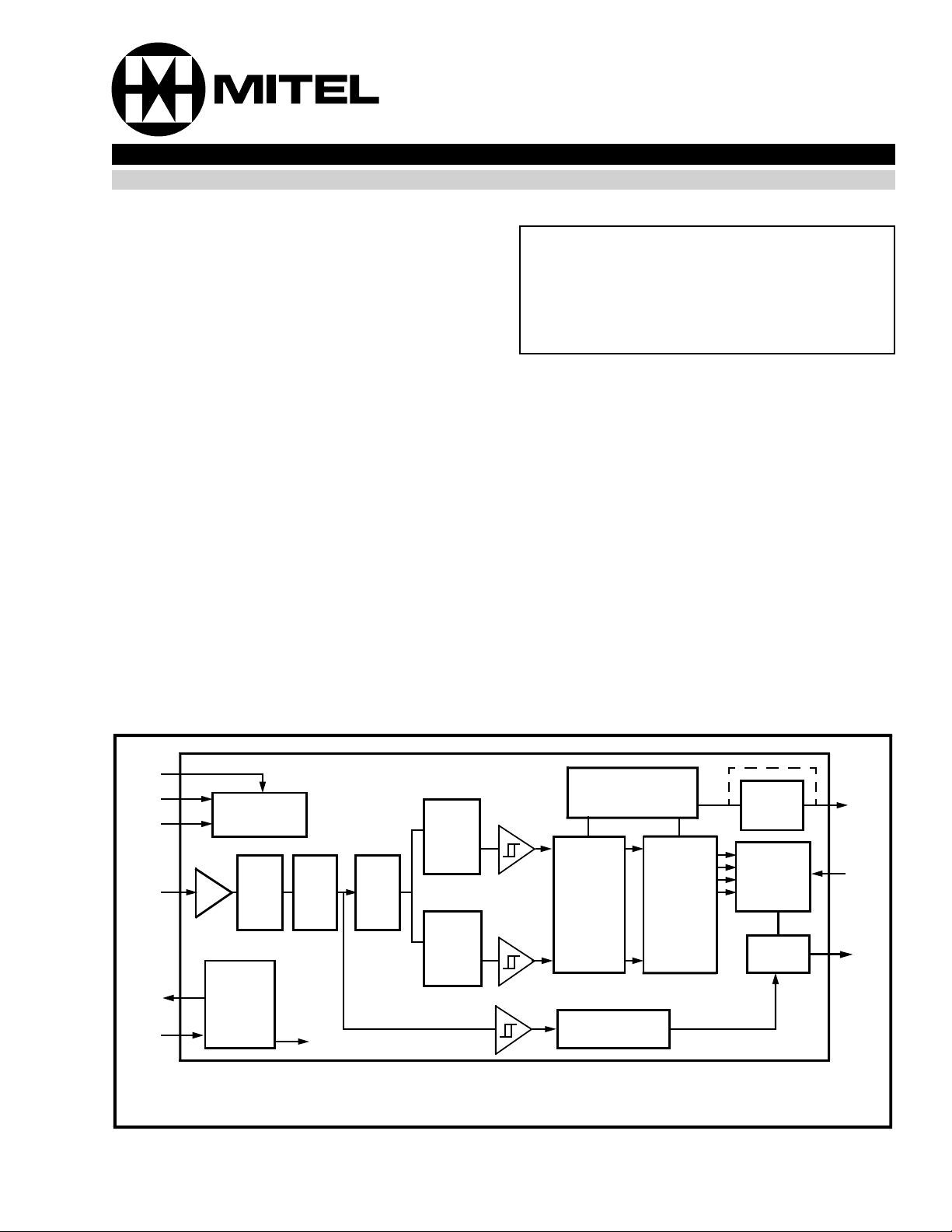
➀
PWDN
VDD
VSS
INPUT
➁
OSC2
OSC1
(CLK)
➀ MT3170B/71B and MT337xB only.
➁ MT3270B/71B and MT337xB only.
➂ MT3x71B only.
Voltage
Bias Circuit
AGC
Filter
Oscillator
and
Clock
Circuit
Antialias
To All Chip Clocks
Dial
Tone
Filter
Figure 1 - Functional Block Diagram
High
Group
Filter
Low
Group
Filter
Digital
Detector
Algorithm
Energy
Detection
Steering
Circuit
Code
Converter
and
Latch
Digital
Guard
➂
Time
Parallel to
Serial
Converter
& Latch
Mux
ESt
or
DStD
ACK
SD
4-3
Page 2
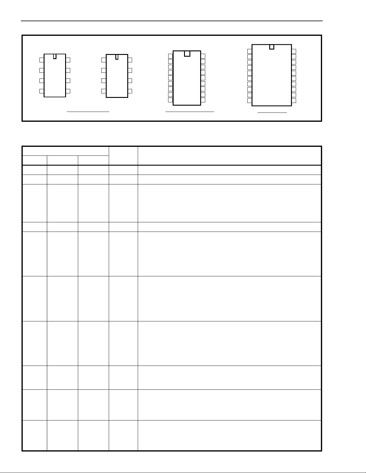
MT3170B/71B, MT3270B/71B, MT3370B/71B
NC
NC
NC
NC
NC
MT3370B/71B
1
2
3
4
5
6
7
8
9
10
20 PIN SSOP
20
19
18
17
16
15
14
13
12
11
MT3170B/71B MT3270B/ 71 B MT3370B/ 71 B
INPUT
PWDN
CLK
VSS
VDD
ESt/
DStD
ACK
SD
INPUT
OSC2
OSC1
VSS
1
2
3
4
1
8
2
7
3
6
4
5
8 PIN PLASTIC DIP
VDD
8
ESt/
7
DStD
ACK
6
SD
5
NC
INPUT
PWDN
OSC2
NC
OSC1
NC
NC
VSS
18 PIN PLASTIC SOIC
1
2
3
4
5
6
7
8
9
18
17
16
15
14
13
12
11
10
VDD
NC
NC
ESt/DStD
NC
ACK
NC
SD
NC
INPUT
PWDN
OSC2
OSC1
VSS
Figure 2 - Pin Connections
Pin Description
Pin #
337xB 327xB 317xB
2 1 1 INPUT DTMF/CP Input. Input signal must be AC coupled via capacitor.
42 -OSC2Oscillator Ou tpu t.
63 3OSC1
94 4V
11 5 5 SD Serial Data/Call Progress Output. This pin serves the dual function
13 6 6 ACK Acknow le dg e Pulse Inpu t . After ESt or DStD is high, applying a
15 7 7 ESt
Name Description
Oscillator/ Cl ock In pu t. This pin can either be driven by:
(CLK )
1) a n external dig ital clock with defi ned input logic levels. OSC2
should be left open.
2) connecting a crystal or ceramic resonator between OSC1 and
OSC2 pins.
Ground. (0V)
SS
of being the serial data output when clo ck pulse s are applied after
validation of DTMF signal, and also indicate s the cadence of call
progress input. As DTMF signal lies in the same frequency band a s
call progress signal, this pin may togg le for DTM F input. The SD pin
is at logic low in powerdown state.
sequence of four pulses on this pin will then shift out four bits on the
SD pin, representing the decoded DTMF digit. The rising edge of the
first clock is used to latch the 4-bit data prior to shifting. This pin is
pulled down internall y. The idle state of the ACK signal should be
low.
Early Steerin g Output. A logic high on ESt indicates that a DTMF
(MT3x70B)
signal is present. ESt is at logic low in powerdown state.
NC
NC
VDD
NC
ESt/DStD
NC
ACK
SD
NC
NC
DStD
(MT3x7 1B)
Delayed Steering Output. A logic high on DStD indicate s that a
valid DTMF digit has been dete cted. DStD is at logic low in
powerdown state.
18 8 8 V
Positive Power Supply (5V Typ.) Performance of the device can be
DD
optimized by minim izing noise on the supply rails. Decoupli ng
1,5,7,8,
capacitors across V
--NCNo Connection. Pin is unconnected internally.
and VSS are therefore recommend ed.
DD
10, 12,
14,16,
17
3- 2PWDNPower Dow n Inpu t. A logic high on this pin will power down the
device to reduce power consumption. This pin is pulled down
internally and can be left open if not used. ACK pin should be at logic
’0’ to power down device.
4-4
Page 3
MT3170B/71B, MT3270B/71B, MT3370B/71B
Summary of MT3x70/71B Product Family
Device
Type
MT3170B ✔✔✔✔
MT3171B ✔✔✔✔
MT3270B ✔✔✔✔
MT3271B ✔✔✔✔
MT3370B ✔✔✔✔✔✔
MT3371B ✔✔✔✔✔ ✔
Functional Description
The MT3x7xBs are high performance and low power
consumption DTMF receivers. These devices
provide wide dynamic range DTMF detection and a
serial decoded data output. These devices also
incorporate an energy detection circuit. An input
voiceband signal is applied to the devices via a
series decoupling capacitor. Following the unity gain
buffering, the signal enters the AGC circuit followed
by an anti-aliasing filter. The bandlimited output is
routed to a dial tone filter stage and to the input of
the energy detection circuit. A bandsplit filter is then
used to separate the input DTMF signal into high
and low group tones. The high group and low group
tones are then verified and decoded by the internal
frequency counting and DTMF detection circuitry.
Following the detection stage, the valid DTMF digit is
translated to a 4-bit binary code (via an internal lookup ROM). Data bits can then be shifted out serially
by applying external clock pulses.
Automatic Gain Control (A GC) Circ uit
As the device operates on a single power supply, the
input signal is biased internally at approximately
VDD/2. With large input signal amplitude (between 0
and approximately -30dBm for each tone of the
composite signal), the AGC is activated to prevent
the input signal from being clipped. At low input
level, the AGC remains inactive and the input signal
is passed directly to the hardware DTMF detection
algorithm and to the energy detection circuit.
Filter and Decoder Section
The signal entering the DTMF detection circuitry is
filtered by a notch filter at 350 and 440 Hz for dial
tone rejection. The composite dual-tone signal is
further split into its individual high and low frequency
components by two 6
bandpass filters. The high group and low group
tones are then smoothed by separate output filters
and squared by high gain limiting comparators. The
8 Pin 18 Pin 20 Pin PWDN
resulting squarewave signals are applied to a digital
detection circuit where an averaging algorithm is
employed to determine the valid DTMF signal. For
MT3x70B, upon recognition of a valid frequency from
each tone group, the early steering (ESt) output will
go high, indicating that a DTMF tone has been
detected. Any subsequent loss of DTMF signal
condition will cause the ESt pin to go low. For
MT3x71B, an internal delayed steering counter
validates the early steering signal after a
predetermined guard time which requires no external
components. The delayed steering (DStD) will go
high only when the validation period has elapsed.
Once the DStD output is high, the subsequen t loss of
early steering signal due to DTMF signal dropout will
activate the internal counter for a validation of tone
absent guard time. The DStD output will go low only
after this validation period.
Energy Detection
The output signal from the AGC circuit is also
applied to the energy detection circuit. The detection
circuit consists of a threshold comparator and an
active integrator. When the signal level is above the
threshold of the internal comparator (-35dBm), the
energy detector produces an energy present
indication on the SD output. The integrator ensures
the SD output will remain at high even though the
input signal is changing. When the input signal is
removed, the SD output will go low following the
integrator decay time. Short decay time enables the
signal envelope (or cadence) to be generated at the
SD output. A n external mic rocontroller c an monitor
this output for specific call progress signals. Since
presence of speech and DTMF signals (above the
threshold limit) can cause the SD output to toggle,
both ESt (DStD) and SD outputs should be
monitored to ensure correct signal identification. As
the energy detector is multiplexed with the digital
serial data out put at the SD pin, the detector output
th
order switched capacitor
is selected at all times except during the time
between the rising edge of the first pulse and the
falling edge of the fourth pulse applied at the ACK
pin.
2 Pin
OSC
Ext
CLK
ESt DStD
4-5
Page 4

MT3170B/71B, MT3270B/71B, MT3370B/71B
Serial Data (SD) O utput
When a valid DTMF signal burst is present, ESt or
DStD will go high. The application of four clock
pulses on the ACK pin will provide a 4-bit serial
binary code representing the decoded DTMF digit on
the SD pin output . The rising edge of the first pulse
applied on the ACK pin latches and shifts the least
significant bit of the decoded digit on the SD pin.
The next three pulses on ACK pin will shift the
remaining latched bits in a serial f ormat (see Figure
5). If less than four pulses are applied to the ACK
pin, new data cannot be latched even though ESt/
DStD can be valid. Clock pulses should be applied
to clock out any remaining data bits to resume
normal operation. Any transitions in excess of four
pulses will be ignored until the next rising edge of the
ESt/DStD. ACK should idle at logic low. The 4-bit
binary representing all 16 standard DTMF digits are
shown in Table 1.
Powerdow n Mod e (MT 317xB /337 xB )
The MT317xB/337xB devices offer a powerdown
function to preserve power consumption when the
device is not in use. A logic high can be applied at
the PWDN pin to place the device in powerdown
mode. The ACK pin should be kept at logic low to
avoid undefined ESt/DStD and SD outputs (see
Table 2).
F
LOW
F
HIGH
DIGIT b
b
3
b
2
1
6971209 1 0001
6971336 2 0010
6971477 3 0011
7701209 4 0100
7701336 5 0101
7701477 6 0110
8521209 7 0111
8521336 8 1000
8521477 9 1001
9411336 0 1010
9411209 * 1011
9411477 # 1100
6971633 A 1101
7701633 B 1110
8521633 C 1111
9411633 D 0000
0= LOGIC LOW, 1= LOGIC HIGH
Table 1. Serial Decode Bit Table
Note: b0=LSB of d ec od ed D T MF di gi t a nd s hi fte d out first.
b
0
ACK (input) PWDN (input) ESt/DStD (output) SD (output)
low low Refer to Fig. 4 for
timing waveforms
low high
+
low low powerdown mode
Refer to Fig. 4 for
timing waveforms
high low low undefined undefined
high h igh undefined undefined undefined
+
=ente rs po w erd ow n m o de on the r is in g ed ge .
Table 2. Powerdown Mode
Frequency 1 (Hz) Frequency 2 (Hz) On/Off Description
350 440 continuous North Ame rican Dial Tones
425 --- continuous European Dia l Ton es
400 --- continuous Far East Dial Tones
480 620 0.5s/0.5s North American Line Busy
440 --- 0.5s/0.5s Japanese Line Busy
480 620 0.25s/0.25s North American Reorder Tones
440 480 2.0s/4.0s North American Aud ible Ring ing
480 620 0.25s/0.25s North American Reorder Tones
Table 3. Call Progress Tones
MT317xB/337xB
status
normal operation
4-6
Page 5

MT3170B/71B, MT3270B/71B, MT3370B/71B
Parameter Unit Re sonator Crystal
R1 Ohms 6.580 25
L1 m H 0.359 95.355
C1 pF 4.441 15.1E-03
C0 pF 34.890 12.0
Qm - 1.299E+03 101.2E+ 03
∆f % ±0.2% ±0.01%
Table 4. Recommended Resonator and Crystal
Specifi cations
Note: Qm=q ua li ty fa ct or o f RLC mo de l, i.e ., 1/2 ΠƒR1C1.
be driven by an 4.194304 MHz external clock applied
on pin OSC 1. The OSC2 pin should be left open.
For MT317xB devices , the CLK input is driven
directly by an 4.194304 MHz external digital clock.
Applications
The circuit shown in Figure 3 illustrates the use of a
MT327xB in a typical receiver application. It requires
only a coupling capacitor (C1) and a crystal or
ceramic resonator (X 1) to c om ple te the circuit.
L1 C1 R1
R1 = Equivalent resistor.
L1 = Equivalent inductance.
C1 = Equivalent compliance.
C0 = Capacitance between electrode.
C0
Resonator and Crystal Electric Equivalent Circuit
Oscillator
The MT327xB/337xB can be used in both external
clock or two pin oscillator mode. In two pin oscillator
mode, the oscillator circuit is completed by
connecting either a 4.194304 MHz crystal or ceramic
resonator across OSC1 and OSC2 pins.
Specifications of the ceramic resonator and crystal
are tabulated in Table 4. It is also possible to
configure a number of these devices employing only
a single oscillator crystal. The OSC2 output of the
first device in the chain is connected to the OSC1
input of the next device. Subsequent devices are
connected similarily. The oscillator circuit can also
The MT3x70B is designed for user who wishes to
tailor the guard time for specific applications. When
a DTMF signal is present, the ESt pin will go high.
An external microcontroller monitors ESt in real time
for a period of time set by the user. A guard time
algorithm must be implemented such that DTMF
signals not meeting the timing requirements are
rejected. The MT3x71B uses an internal counter to
provide a preset DTMF validation period. It requires
no external components. The DStD output high
indicates that a valid DTMF digit has been detected.
The 4.194304 MHz frequency has a secondary
advantage in some applications where a real time
clock is required. A 22-bit counter will count
4,194,304 cycles to provide a one second time base.
DTMF/CP Input
X1
COMPONENTS LIST:
C1 = 0.1 µF ± 10 %
X1 = Crystal or Resonator (4.194304 MHz)
Figure 3 - Application Circuit for MT327xB
C1
1
2
3
4
INPUT
OSC2
OSC1
V
SS
MT327xB
ESt/DStD
V
DD
ACK
SD
V
8
7
6
5
DD
To microprocessor or
microcontroller
4-7
Page 6

MT3170B/71B, MT3270B/71B, MT3370B/71B
Absolute Maximum Ratings
†
- Voltages are with respect to V
=0V unless otherwise stated.
SS
Parame ter Symbol Min Max Units
1 DC Power S upply Voltage V
2 Voltage on any pin (other than supply) V
3 Current at any pin (other than supply) I
4 Storage t emperature T
5 Package power dissipation P
† Exceeding these values may cause permanent damage. Functional operation under these conditions is not implied.
Recommended Operating Conditions - Voltages are with respect to V
Parameter Sym Min Typ
1 Positive Power Su pply V
2 Oscillator Clock Frequency f
3 Oscillator Frequency Tol erance ∆f
OSC
OSC
4 Operating T e mperature T
‡ Typical figures are at 25°C and are for design aid only: not guaranteed and not subject to producti on testing.
4.75 5.0 5.25 V
DD
-40 25 85 °C
d
DD-VSS
I/O
I/O
S
D
‡
4.194304
-0.3 6.3 V
-65 150 °C
=0V unless otherwise stated
SS
Max Units Test Conditions
MHz
±0.1 %
6V
10 mA
500 mW
DC Electrical Characteristics - Voltages are with respect to V
otherwise stated.
Characteristics Sym Min Typ
1 Operating supply current I
2 Standby supply current I
3a Input logic 1 V
3b Input logic 1
DD
DDQ
IH
V
IH
4.0 V
3.5 V MT327xB/MT 337xB
=5V±5%,VSS=0V, and temperature -40 to 85°C, unless
DD
‡
Max Units Test Conditions
38mA
30 100 µA PWDN=5V, ACK=0V
(for OSC1 input only)
4a Input logic 0 V
4b Input logic 0
IL
V
IL
1.0 V
1.5 V MT327xB/MT 337xB
(for OSC1 input only)
5 Input impedance (pin 1) R
6 Pull-down Current
IN
I
PD
50 kΩ
25 µA with internal pull-down
(PWDN, ACK pin s)
7 Output high (source) current I
8 Output low (sink) current I
‡ Typical figures are at 25°C and are for design aid only: not guaranteed and not subject to producti on testing
OH
OL
0.4 4.0 mA V
1.0 9.0 mA V
ESt/DStD = SD = 0V
resistor of approx.
200kΩ. PWDN/ACK = 5V
OUT=VDD
OUT=VSS
-0.4V
+0.4V
4-8
Page 7

MT3170B/71B, MT3270B/71B, MT3370B/71B
AC Electrical Characteristics - voltages are with respect to V
otherwise stated.
Characteristics Sym Min Typ
1 Valid input signal level
(each tone of composite si gnal)
-50
2.45
=5V±5% , VSS=0V and temperature -40 to +85°C unless
DD
‡
Max Units Tes t Co ndi tions*
0
775
dBm
mV
1,2,3,5, 6, 1 2
RMS
2 Positive twist accept 8 dB 1,2,3,4,11,12,15
3 Negative twist accept 8 dB 1,2,3,4,11,12,15
4 Frequency deviation accept
5 Frequency deviation reject
±1.5%± 2Hz 1,2,3,5, 1 2
±3.5% 1,2,3,5, 12, 1 5
6 Third tone tolerance -16 dB 1,2,3,4,5,12
7 Noise tolerance -12 dB 7,9,12
8 Dial tone tole ra nce +15 dB 8,10,12
9 Superviso r y tones detect level
-35 dBm 16
(Total power)
10 Supervisor y tones reject level -50 dBm 16
11 Ene rgy det ecto r atta ck ti me t
12 Energy detector decay time t
13a
Powerdown time
13b
Powerup time
SA
SD
325ms16
10
1.0 6.5 ms 16
30
50
ms
ms
ms
IDDQ
MT3170B/3370B
MT3171B/3371B
≤ 100µA
Note 14
14 Tone present det ect time (ESt
t
DP
3 13 20 ms MT3x70B
logic output)
15 Tone absent detect time (ES t
t
DA
3 1 5 ms M T3x70B
logic output)
16 Tone durat ion ac cept
t
REC
40 ms MT3x71B
(DStD logic output)
17 Tone durat ion reject
t
REC
20 ms MT3x71B
(DStD logic output)
18 Interdigit pause accept (DStD
t
ID
40 ms MT3x71B
logic output)
19 Interdigit pause reject (DStD
t
DO
20 ms MT3x71B
logic output)
20 Data shift rate 40-6 0% duty c ycle f
21 Propagation delay
ACK
t
PAD
(ACK to Data Bit)
22 Data hol d tim e (ACK to SD ) t
‡ Typical figures are at 25 °C and are for design aid only: not guaranteed and not subject to produ ctio n testing
* Test Conditions 1. dBm refers to a reference power of 1 mW delivered into a 600 ohms load.
2. Data se qu en c e c o ns is ts o f a ll DTMF d ig it s.
3. Tone o n = 4 0 m s , ton e off = 40 m s .
4. Signal condition consists of nominal DTMF frequencies.
5. Both to ne s in co m po si te s ign a l h av e an equal am p lit ude.
6. Tone pair is deviated by ±1.5%± 2 Hz.
7. Band w id th limite d (0-3 k Hz) G au ss ia n no is e.
8. Precise dial tone frequencies are 350 Hz and 440 Hz (± 2%).
9. Referenced to lowest level frequency component in DTMF signal.
10. Referenced to the minimum valid accept level.
11. Both tone s mu st be w i thi n va li d i np ut s ig na l r a ng e.
12. Exter nal guard time for MT3x70B = 20ms.
13. Timin g pa ram eters ar e me a su red with 70 pF lo ad at SD ou tput.
14. Time du r at io n b et w ee n P WD N pin c ha ng e s fr om ‘ 1‘ to ‘0 ‘ an d ESt/DStD b ec om e s ac tive .
15. Gua r an te ed b y design an d ch ar ac terization . Not subje ct to pro d uc tio n testing .
16. Value me as ure d with a n ap pl ied tone of 4 50 H z .
DH
30 50 ns 13,15
1.0 3.0 MHz 13,15
100 140 ns 1MHz f
13,15
ACK
,
4-9
Page 8

MT3170B/71B, MT3270B/71B, MT3370B/71B
t
REC
t
DO
t
DP
t
REC
DTMF
Tone #n
t
DA
t
ID
INPUT
ESt
(MT3x70B)
DStD
(MT3x71B)
ACK
LSB
MSB
SD
b
0b1b2b3
t
DO
- maximum allowable dropout during valid DTMF signals. (MT3x7xB).
t
- minimum time between valid DTMF signals (MT3x71B).
ID
t
- maximum DTMF signal duration not detected as valid (MT3x7xB).
REC
t
- minimum DTMF signal duration required for valid recognition (MT3x71B).
REC
t
- time to detect the absence of valid DTMF signals (MT3x70B).
DA
t
- time to detect the presence of valid DTMF signals (MT3x70B).
DP
t
- supervisory tone integrator attack time (MT3x7xB).
SA
t
- supervisory tone integrator decay time (MT3x7xB).
SD
DTMF
Tone #n + 1
LSB
MSB
b0b1b2b
3
DTMF
Tone
#n + 1
Input
Signal
t
SA
t
SD
Input
Signal
Envelope
ESt/DStD
ACK
SD
4-10
V
IH
V
IL
V
IH
V
IL
DTMF Energy
Detect
t
PAD
1/f
ACK
Figure 4 - Timing Diagram
b
LSB
0
b
1
Figure 5 - ACK to SD Timing
t
DH
b
2
b
3
DTMF Energy
Detect
MSB
 Loading...