

Page 1
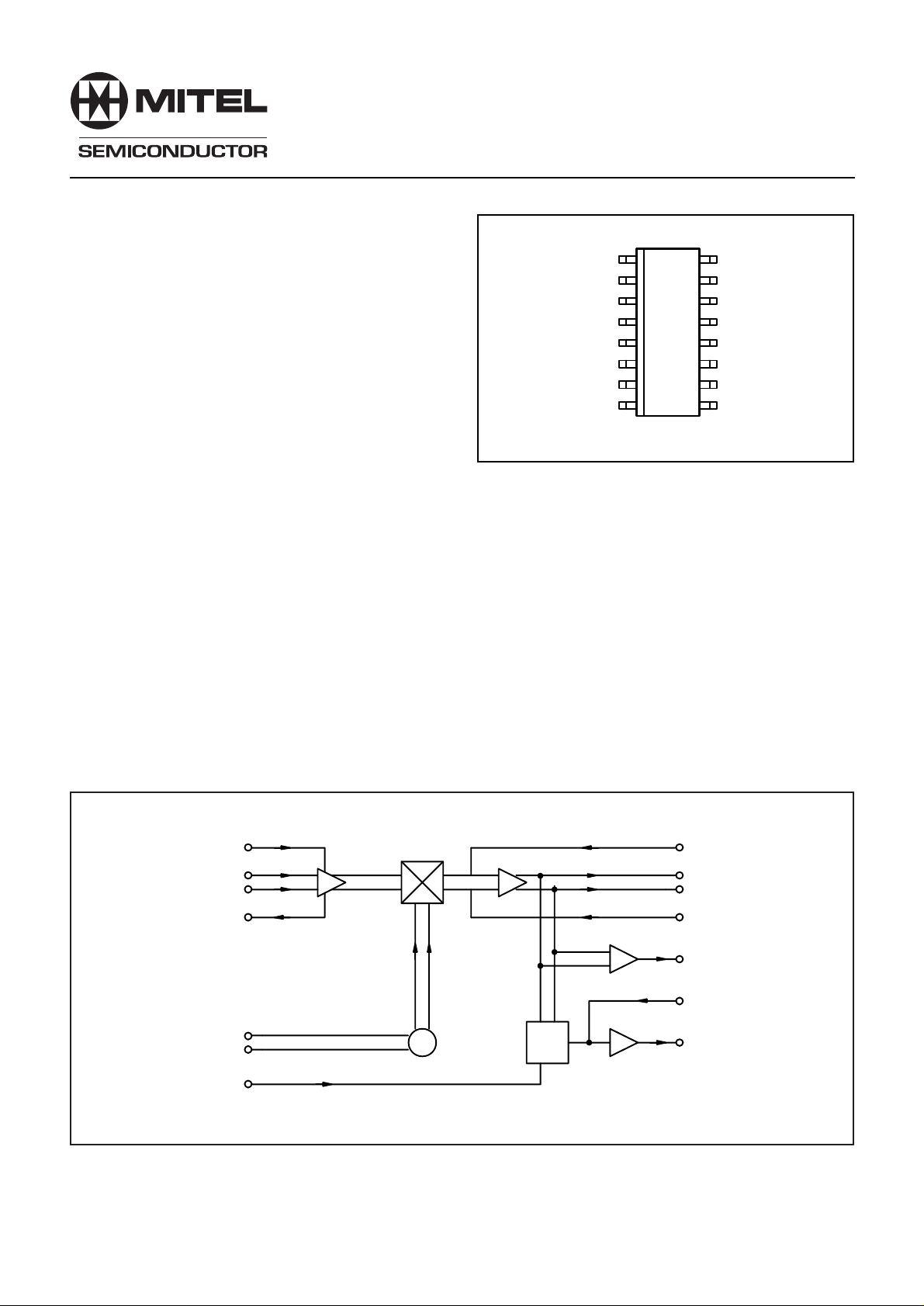
The SL1461SA is a wideband PLL FM demodulator,
intended primarily for application in satellite tuners.
The device contains all elements necessary, with the
exception of external oscillator sustaining network and loop
feedback components, to form a complete PLL system
operating at frequencies up to 800MHz.
An AFC with window adjust is provided, whose output
signal can be used to correct for any frequency drift at the head
end local oscillator.
FEATURES
■ Single chip PLL system for wideband FM
demodulation
■ Simple low component count application
■ Allows for application of threshold extension
■ Fully balanced low radiation design
■ High operating input sensivity
■ Improved VCO stability with variations in supply or
temperature
■ AGC detect and bias adjust
■ 75Ω video output drive with low distortion levels
■ Dynamic self biasing analog AFC
■ Full ESD Protection*
* Normal ESD handling procedures should be observed
Wideband PLL FM Demodulator
Advance Information
DS4049 - 1.2 December 1994
AFC PUMP
AFC WINDOW ADJUST
EE
V
OSCILLATOR +
OSCILLATOR –
AGC BIAS
AGC OUTPUT
RF INPUT
Fig.1 Pin connections - top view
APPLICATIONS
■ Satellite receiver systems
■ Data communications Systems
ORDERING INFORMATION
SL1461SA/KG/MPAS
16116
2
15
3
14
4
13
5
12
SL1461SA
6
11
10
7
89
SL1461SA
AFC OUTPUT
V
CC
VIDEO FEEDBACK +
VIDEO –
VIDEO +
VIDEO FEEDBACK –
VIDEO OUTPUT
RF INPUT
MP16
AGC BIAS
RF INPUTS
AGC OUTPUT
LOCAL
OSCILLATOR
AFC WINDOW
ADJUST
6
8
9
7
4
5
2
14
VIDEO
FEEDBACK +
12
VIDEO +
13
VIDEO –
11
VIDEO
FEEDBACK –
10
VIDEO
OUTPUT
1
AFC PUMP
16
AFC OUTPUT
Fig.2 SL1461SA block diagram
Page 2
SL1461SA
ELECTRICAL CHARACTERISTICS
T
= -20°C to +80°C, VCC = +4.5V to +5.5V. The electrical characteristics are guaranteed by either production test or design.
amb
They apply within the specified ambient temperature and supply voltage unless otherwise stated.
Characteristics
Supply current
Operating frequency
Input sensitivity
Input overload
VCO sensitivity (dF/dV)
VCO linearity
VCO supply stability
VCO temperature stability
Phase detector gain
Loop amplifier input impedance
Loop amplifier output impedance
Loop amplifier open loop gain
Loop amplifier gain bandwidth product
Loop amplifier output swing
Video drive output impedance
Video drive:
Luminance nonlinearity
- differential gain
- differential phase
- intermodulation
- signal/noise
- Tilt
- baseline distortion
AGC output current
AGC bias current
AFC window current
AFC charge pump current
AFC leakage current
AFC output saturation voltage
Value
Min. Typ. Max.
36
300
40
800
-40
0
25
32
39
25
2.0
20
0.5
0.25
450
570
700
25
38
240
1.2
55
75
1.9
0.5
1.0
95
5
2.5
3
-40
66
10
0
0
72
0.3
0.4
3
2
400
250
400
50
10
0.4
Units
mA
MHz
dBm
dBm
MHz/V
%
MHz/V
KHz/°C
V/rad
V/rad
Ω
Ω
dB
MHz
Vp-p
Ω
%
%
Degree
dB
dB
%
%
µA
µA
µA
µA
µA
V
Conditions
Preamp limiting
Refer to application in Fig. 3
Refer to application in Fig. 3; with
13.5MHz p-p deviation
See note 5
See note 5
Differential loop filter
Single ended loop filter
Single ended
Single ended
Single ended
Single ended
Single ended
1KΩ load, See note 3 and 4
75KΩ load, See note 3 and 4
75KΩ load, See note 3 and 4
See notes 1, 3 and 4
1KΩ load, See note 2 and 4
1KΩ load, See note 3 and 4
1KΩ load, See note 3 and 4
Maximum load voltage drop 2V
400µA gives 1.5V deadband window
With charge pump disabled
AFC output enabled
Note 1. Product of input modulation f 1 at 4.43MHz, 13.5MHz p–p deviation and f 2 at 6MHz p–p deviation, (PAL chroma and sound
subcarriers).
Note 2. Ratio of output video signal with input modulation at 1MHz, 13.5MHz p–p deviation, to output rms noise in 6MHz bandwidth with
no input modulation.
Note 3. Input test signal pre–emphasised video 13.5MHz p–p deviation. Output voltage 600mV pk–pk.
Note 4. See page 3
Note 5. Assuming operating frequency of 479.5MHz set with V
shown in Fig. 3. also refer to Fig. 8.
@ 5.0V and ambient temperature of +20°C. Only applies to Application
CC
2
Page 3

SL1461SA
TEST CONFIGURATION
VIDEO GENERATOR
ROHDE & SCHWARZ SGPF
PRE EMPHASISED BASE BAND VIDEO
DE EMPHASISED BASE BAND VIDEO 1V p–p
The video drive characteristics measurements were made using the above test configuration. The maximum figures recorded in
the Electrical Characteristics Table coincide with high temperatures and extremes of supply voltage. No adjustment to the recorded
figures has been made to compensate for the effects of temperature on the external components of the application test board, in
particular the varactor diodes. If operation of the device at high ambient temperatures is envisaged then attention to temperature
compensation of the external circuitry will result in performance figures closer to the stated typical figures.
BASE BAND VIDEO 1V p–p
ROHDE & SCHWARZ SFZ
RF CARRIER FREQ 479.5MHz
FM MODULATION 13.5MHz P–P
PRE–EMPHASISED VIDEO
MONTFORD
TEST OVEN
SL1461 TEST APPLICATION BOARD
See Fig. 3 for details
DE EMPHASISED NETWORK
ROHDE & SCHWARZ UAF
TV SAT TEST TX
VIDEO AMPLIFIER/
VIDEO ANAL YSER
ABSOLUTE MAXIMUM RATINGS
All voltages are referred to VEE at 0V
Characteristics
Supply voltage
RF input voltage
RF input DC offset
Oscillator ± DC offset
Video ± DC offset
Video feedback ± DC offset
Video output DC offset
AFC pump DC offset
AFC disable DC offset
AFC deadband DC offset
AGC bias DC offset
AGC output DC offset
Storage temperature
Junction temperature
MP16 package thermal resistance,
chip to ambient
Fig.2 SL1461SA block diagram
Min. Typ. Max.
-0.3
-0.3
-0.3
-0.3
-0.3
-0.3
-0.3
-0.3
-0.3
-0.3
-0.3
-55
7
2.5
V
+0.3
CC
V
+0.3
CC
V
+0.3
CC
VCC+0.3
V
+0.3
CC
V
+0.3
CC
V
+0.3
CC
VCC+0.3
V
+0.3
CC
V
+0.3
CC
125
150
111
V
Vp-p
V
V
V
V
V
V
V
V
V
V
°C
°C
°C/W
Conditions
3
Page 4
SL1461SA
ABSOLUTE MAXIMUM RATINGS cont.
All voltages are referred to V
Characteristics
EE
at 0V
Min. Typ. Max.
Conditions
MP16 package thermal resistance,
chip to case
Power consumption at 5.5V
ESD protection - pins 1 to 15
ESD protection - Pin 16
2K
AGC BIAS AFC WINDOW ADJUST
RV1 RV2
D1
BB515
BB515
D2
C5
470nF
TP3
4n7
C6
2
1.7
50K
47nF 100nF
R1
4K7
R2
5K1
R3
4K7
41
250
1nF
°C/W
mW
kV
kV
27K
C2C1
16116
2
15
3
14
4
13
5
12
SL1461SA
6
11
10
7
89
C8C7
Mil-std-883 method 3015 class 1
Mil-std-883 method 3015 class 1
R6
R5
1K2
R4
1K2
1nF
TP4
C9
100pF
47
100nF
C11
C10
F
C3
TP1
TP2
100pF
F
47
C4
VIDEO OUTPUT
+5V
1nF
C12
RF INPUT
Fig.3 Standard application circuit
FUNCTIONAL DESCRIPTION
The SL1461SA is a wideband PLL FM demodulator,
optimised for application in satellite receiver systems and
requiring a minimum external component count. It contains all
the elements required for construction of a phase locked loop
circuit, with the exception of tuning components for the local
oscillator, and an AFC detector circuit for generation of error
signal to correct for any frequency drift in the outdoor unit local
oscillator. A block diagram is contained in Fig. 2 and the typical
application in Fig. 3.
The internal pin connections are contained in Fig.6/6a
In normal applications the second satellite IF frequency of
typically 402 or 479.5MHz is fed to the RF preamplifier, which
has a working sensitivity of typically -40 dBm, depending on
application and layout. The preamplifier contains an RF level
detect circuit, which generates an AGC signal that can be used
for controlling the gain of the IF amplifier stages, so maintaining
a fixed level to the RF input of the SL1461SA, for optimum
threshold performance. The bias point of the AGC circuit can
be adjusted to cater for variation in AGC line voltage
requirement and device input power. The typical AGC curves
are shown in Fig. 9. It is recommended that the device is
operated with an input signal between -30 and -35dBm. This
ensures optimum linearity and threshold performance, and
gives a good safety margin over the typical sensitivity of
-40dBm.
The output of the preamplifier is fed to the mixer section
which is of balanced design for low radiation. In this stage the
RF signal is mixed with the local oscillator frequency, which is
generatedby an on–board oscillator. The oscillator block uses
an external varactor tuned sustaining network and is optimised
for high linearity over the normal deviation range. A typical
frequency versus voltage characteristic for the oscillator is
contained in Fig. 7. The loop output is designed to compensate
for first order temperature variation effects; the typical stability
is shown in Fig. 8
The output of the mixer is then fed to the loop amplifier
around which feedback is applied to determine loop transfer
characteristic . Feedback can be applied either in differential or
single ended mode; if the appropriate phase detector gains are
assumed in calculating loop filters, both modes should give the
same loop response.
The loop amplifier drives a 75Ω output impedance buffer
amplifier, which can either be connected to a 75Ω load or used
to drive a high input impedance stage giving greater linearity
and approximately 6dB higher demodulated signal output
level.
4
Page 5

DESIGN OF PLL LOOP PARAMETERS
where:
K
0
is the VCO gain in radian seconds per volt
K
D
is the phase detector gain in volts per radian
n
is the natural loop bandwidth
is the loop damping factor
R1 is loop amplifier input impedance
Note: K
0
is dependant on sensitivity of VCO used.
K
D
= 0.25V/rad single ended, 0.5V/rad differential
From these factors the loop 3dB bandwidth can be determined
from the following expression;
SL1461SA
GAIN = K
VCO
VOLT/RAD
D
GAIN = K
The SL1461SA is normally used as a type 1 second order
loop and can be represented by the above diagram. For such
a system the following parameters apply;
1
2
and
R2
RAD SEC/VOLT
0
Fig.4
C1
BASEBAND OUTPUTR1RF INPUT
K0K
1
2
D
2
n
2
n
AFC FACILITY
The SL1461SA contains an analog frequency error detect
circuit, which generates DC voltage proportional to the integral
of frequency error. If the incident RF is high then the AFC
voltage increases, if low then the voltage decreases. The AFC
voltage can then be converted by an ADC to be read by the
micro controller for frequency fine tuning; if used in an I2C
system it is recommended the device is used with either the
SP5055 or SP5056 frequency synthesiser which contains an
internal ADC readable via the I2C bus.
The voltage corresponding to frequency alignment is
arbitrary and user defined; if used with the SP5055 it is
suggested the aligned voltage is 0.375 VCC , corresponding to
the centre code of the ADC on port 6.
The AFC detect circuit contains a deadband centre
around the aligned frequency. The deadband can be adjusted
from zero window to approximately 25MHz width assuming an
oscillator dF/dV of 15MHz/V. If the incident RF is within this
window the AFC voltage does not integrate, except by
component leakage.
With reference to Fig.5; in normal operation the
demodulated video is fed to a dual comparator where it is
compared with two reference voltages, corresponding to the
extremes of the deadband, or window. These voltages are
variable and set by the window adjust input.
The comparators produce two digital outputs
corresponding to voltages above or below the voltage window,
or frequency above or below deadband. These digital control
signals are used to control a complimentary current source
pump. The current signals are then fed to the input of an
amplifier which is arranged as an integrator, so integrating the
pulses into a DC voltage.
If the frequency is correctly aligned both the current
source and sink are disabled, therefore the DC output voltage
remains constant. There will be a small drift due to component
leakage; the maximum drift can be calculated from;
5
Page 6

SL1461SA
BASEBAND
VIDEO
WINDOW
ADJUST
FREQ
V
V
ALIGN
V
HI
LO
V
CC
CC
V
+
–
C
EXT
R
V
AFC
EXT
+
–
V
EE
Fig.5 AFC system block diagram
6
Page 7

V
REF; 2.7V
V
CC
AGC OUTPUT
V
REF; 2V
SL1461SA
AGC BIAS
V
REF; 3V
RF INPUTS
AGC output
2x1500
10K
V
CC
AFC PUMP
V
REF; 1.6V
AGC bias adjust
AFC WINDOW
AFC window adjustRF inputs
VIDEO +
AFC output stage
AFC OUTPUT
Fig.6 SL1461SA I/O port internal circuitry
330 330
2mA 2mA
Video amp outputs
VIDEO –
7
Page 8

SL1461SA
REF; 1.2V
V
OSCILLATOR +
OSCILLATOR –
2 x 5k
Local oscillator
FROM PHASE DETECTOR
2x570
VIDEO
FEEDBACK +
VIDEO
FEEDBACK –
Video amp feedback inputs
Fig.6a SL1461SA I/O port internal circuitry
FREQ MHz
520
500
480
V
CC
68
105
4mA
Video output drive
VIDEO
OUTPUT
460
440
420
400
360
1 1.5 2 2.5 3 3.5 4 4.5 5
DC VOLTAGE
Fig.7 Typical VCO frequency vs DC control voltage
8
Page 9

480
479.5
SL1461SA
VCO STABILITY vs TEMP and SUPPLY
AGC
OUTPUT
VOLTAGE
479
478.5
478
477.5
477
FREQUENCY (MHz)
476.5
476
475.5
–20 30 80
555
TEMP/°C
SUPPLY (V)
Fig.8 SL1461SA VCO centre frequency uncompensated temperature stability
2.0
1.5
1.0
AGC BIAS RESISTOR 5.1K
AGC BIAS CURRENT 297 A
0.5
–70 –60 –50 –40 –30 –20 –10 0
AGC LOAD RESISTOR 3.9K
AGC BIAS RESISTOR 10.5K
AGC BIAS CURRENT 150
AGC LOAD RESISTOR 4.7K
AGC BIAS RESISTOR 32K
AGC BIAS CURRENT 52
AGC LOAD RESISTOR 10K
4.5
4.75
5
5.25
5.5
A
A
RF INPUT LEVEL (dBm) UNMODULATED
Fig.9 SL1461SA AGC output voltage for differing values of AGC bias resistor
APPLICATION NOTES
Capture range
Under conditions when there is no RF input signal present,
the SL1461SA may react to spurious radiation from the free
running oscillator coupling into the RF inputs. Because of the
constant phase error between the VCO input to the phase
detector and the spuriously coupled signal via the RF input, the
phase comparator will drive the control voltage to either the
bottom or the top of the range.
In such a case, the capture range will be asymmetrical
about the VCO free running frequency, since any control
voltage will only be able to tune the VCO in one direction if the
tuning voltage is already at the max or min.
This effect can be avoided by driving the RF input
differentially or achieving good common mode rejection to the
VCO signal.
The lock range is independant of the above effects and will
be symmetric about the centre of the phase detector S-curve
CC
= 5.0 VOLTS
V
provided the VCO is correctly aligned.
EXAMPLE
Loop out of lock
Tuning voltage =4.3V (maximum)
frequency =520MHz (maximum
It is only possible to capture signals below this frequency since
the VCO is already at its maximum frequency.
Testing of capture range should be done with the device
operating under normal conditions. An input signal of between
-35dBm to -10dBm is suitable for such a measurement.
9
Page 10

SL1461SA
Lock range
Lock range should be symmetric about the centre of the
S-curve. When the oscillator is sitting in the centre of the
S-curve, the two video outputs will be at the same DC voltage.
RF oscillator design
The standard application circuit for the SL1461SA is
shown in Fig.3 The layout of the VCO tank should follow normal
good RF techniques - ie as compact as possible. This will
minimise parasitics, thus giving improved VCO linearity and
stability. The PCB layout used for testing purpose is shown in
Fig. 10.
Setting up of oscillator
The VCO should be set up so that the desired input RF
frequency is at the centre of the lock range. This will coincide
with the centre of the S-curve and the point at which the AFC
toggles when set to zero deadband.
The easiest way to centralise the VCO is to input an RF
carrier which is being modulated by a low frequency
squarewave. The tuning coil(s) should be adjusted until the
AFC voltage toggles between 0.2V and V
the FM deviation of the squarewave used, the more accurate
the setting will be.
A pre-emphasised video input containing black to white
transitions can also be used for this setting, since the DC
content in a pre-emphased video is much less than that in non
pre–emphasised video. This is important as any dc content in
the input waveform will introduce an offset in the AFC transition
point.
The setting can be confirmed by measuring the DC
voltage on the two video outputs, the voltages should be the
same when the oscillator is centred around the incoming
frequency. This DC measurement must be carried out with an
unmodulated carrier of the required frequency. Modulation
must not be present, since by definition, the dc voltages would
be changing, thus making accurate measurement difficult.
CC-0.7V
. The smaller
10
Page 11

SL1461SA
Fig.10 Layout of demo board with component locations
11
Page 12

SL1461SA
PACKAGE DETAILS
Dimensions are shown thus: mm (in).
9·80/10·01
(0·386/0·394)
0·19/0·25
(0·008/0·010)
CHAMFER
REF.
PIN 1
0·33/0·51
(0·013/0·020)
0·69 (0·027)
MAX
16
SPOT REF.
16 LEADS AT
1·27 (0·050)
NOM SPACING
0·25/0·50
3·80/4·00
(0·150/0·157)
5·80/6·20
(0·228/0·244)
(0·010/0·020)
×45°
0-8°
NOTES
1. Controlling dimensions are inches.
0·10/0·25
(0·004/0·010)
1·35/1·75
(0·053/0·069)
2. This package outline diagram is for guidance
only. Please contact your Mitel Semiconductor
Customer Service Centre for further
16-LEAD MINIATURE PLASTIC DIL - MP16
0·40/1·27
(0·016/0·050)
Internet: http://www.mitelsemi.com
●
CUSTOMER SERVICE CENTRES
●
FRANCE & BENELUX Les Ulis Cedex
Tel: (1) 69 18 90 00 Fax: (1) 64 46 06 07
●
GERMANY Munich Tel: (089) 419508-20 Fax: (089) 419508-55
●
ITALY Milan Tel: (02) 6607151 Fax: (02) 66040993
●
JAPAN Tokyo Tel: (03) 5276-5501 Fax: (03) 5276-5510
●
KOREA Seoul Tel: (2) 5668141 Fax: (2) 5697933
●
NORTH AMERICA Scotts Valley, USA
Tel: (408) 438 2900 Fax: (408) 438 5576/6231
© Mitel Corporation 1998 Publication No. DS4049 Issue No. 1.2 December 1994 TECHNICAL DOCUMENTATION – NOT FOR RESALE. PRINTED IN UNITED KINGDOM
This publication is issued to provide information only which (unless agreed by the Company in writing) may not be used, applied or reproduced for any purpose nor form part of any order or contract nor to be regarded
as a representation relating to the products or services concerned. No warranty or guarantee express or implied is made regarding the capability, performance or suitability of any product or service. The Company
reserves the right to alter without prior notice the specification, design or price of any product or service. Information concerning possible methods of use is provided as a guide only and does not constitute any
guarantee that such methods of use will be satisfactory in a specific piece of equipment. It is the user's responsibility to fully determine the performance and suitability of any equipment using such information and
to ensure that any publication or data used is up to date and has not been superseded. These products are not suitable for use in any medical products whose failure to perform may result in significant injury
or death to the user. All products and materials are sold and services provided subject to the Company's conditions of sale, which are available on request.
All brand names and product names used in this publication are trademarks, registered trademarks or trade names of their respective owners.
SOUTH EAST ASIA Singapore
Tel:(65) 333 6193 Fax: (65) 333 6192
●
SWEDEN Stockholm Tel: 46 8 702 97 70 Fax: 46 8 640 47 36
●
TAIWAN, ROC Taipei Tel: 886 2 25461260 Fax: 886 2 27190260
●
UK, EIRE, DENMARK, FINLAND & NORWAY
Swindon Tel: (01793) 726666 Fax : (01793) 518582
These are supported by Agents and Distibutors in major countries
worldwide.
12
 Loading...