

Page 1
MOS-TECH Semiconductor Co.,LTD
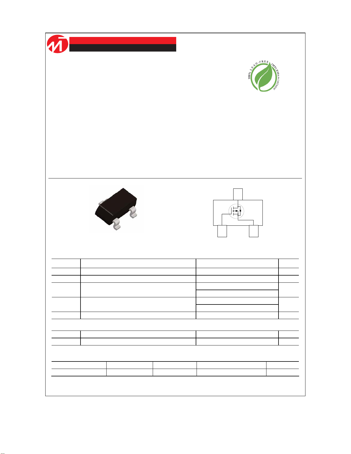
MT2301
Single P-Channel Power MOSFET
MT2301
General Description
This P-Channel Power MOSFET is pro duced
using MOS-TECH Semiconductor’s advanced
PowerTrench process that has b een especially tailored
to minimize the on-state r esistance and yet maintain
low gate charge for superior switching performance.
These devices a re well suit ed for portable electronics
applications: load s witching and power management,
battery charging circuits and DC/DC conversion.
D
Features
• –3.3 A, –20 V. R
R
• Low gate charge (3.6 nC typical)
• High performance trench technology for extremely
low R
• SuperSOT
higher power handling capability than SOT23 in
the same footprint
DS(ON)
TM
-23 provides low R
= 0.072 Ω @ VGS = –4.5 V
DS(ON)
= 0.096Ω @ VGS = –2.5 V
DS(ON)
DS(ON)
D
and 30%
S
G
SOT -23
TM
Absolute Maximum Ratings T
G
o
=25
C unless otherwise noted
A
Symbol Parameter Ratings Units
V
Drain-Source Voltage –20 V
DSS
V
Gate-Source Voltage
GSS
ID Drain Current – Continuous (Note 1a)
– Pulsed –10
Maximum Power Dissipation (Note 1a) 0.5 PD
TJ, T
Operating and Storage Junction Temperature Range –55 to +150
STG
(Note 1b)
±12
3.3
–
0.46
S
V
A
W
°C
Thermal Characteristics
R
θJA
R
θJC
Thermal Resistance, Junction-to-Ambient
Thermal Resistance, Junction-to-Case
(Note 1a) 250
(Note 1) 75
°C/W
°C/W
Package Marking and Ordering Information
Device Marking Device Reel Size Tape width Quantity
010X MT2301 7’’ 8mm 3000 units
©2010 MOS-TECH Semiconductor Corporation www.mtsemi.com Rev.D
Page 2
Electrical Characteristics (T
= 25 OC unless otherwise noted )
A
Symbol Parameter Conditions Min Typ Max Units
OFF CHARACTERISTICS
BV
∆BV
I
DSS
DSS
DSS
Drain-Source Breakdown Voltage VGS = 0 V, ID = -250 µA -20 V
Breakdown Voltage Temp. Coefficient
/∆T
J
Zero Gate Voltage Drain Current
ID = -250 µA, Referenced to 25 oC
VDS = -16 V, V
GS
= 0 V
-1 µA
TJ = 55°C
I
GSSF
I
GSSR
Gate - Body Leakage, Forward VGS = 8 V, VDS = 0 V 100 nA
Gate - Body Leakage, Reverse
VGS = -8 V, V
DS
= 0 V
ON CHARACTERISTICS (Note 2)
V
∆V
R
GS(th)
GS(th)
DS(ON)
Gate Threshold Voltage VDS = VGS, ID = -250 µA -0.8 -1.5 V
Gate Threshold Voltage Temp. Coefficient
/∆T
J
Static Drain-Source On-Resistance
ID = -250 µA, Referenced to 25 oC
VGS = -4.5 V, ID = -1.3 A
TJ =125°C 0.12 0.15
VGS = -2.5 V, I D = -1.1 A
I
g
D(ON)
FS
On-State Drain Current VGS = -4.5 V, VDS = -5 V -3.3 A
Forward Transconductance
VDS = -4.5 V, ID = -2 A
DYNAMIC CHARACTERISTICS
C
iss
C
oss
C
rss
Input Capacitance VDS = -10 V, VGS = 0 V,
Output Capacitance 80 pF
f = 1.0 MHz
Reverse Transfer Capacitance 35 pF
SWITCHING CHARACTERISTICS (Note 2)
t
t
t
t
Q
Q
Q
D(on)
r
D(off)
f
g
gs
gd
Turn - On Delay Time
Turn - On Rise Time 12 22 ns
VDD = -5 V, ID = -0.5 A,
VGS = -4.5 V, R
GEN
= 6 Ω
Turn - Off Delay Time 16 26 ns
Turn - Off Fall Time 5 12 ns
Total Gate Charge
Gate-Source Charge 0.8 nC
VDS = -10 V, ID = - 2 A,
VGS = -4.5 V
Gate-Drain Charge 0.7 nC
DRAIN-SOURCE DIODE CHARACTERISTICS AND MAXIMUM RATINGS
I
S
V
SD
Note:
1. R
is the sum of the junction-to-case and case-to-ambient thermal resistance where the case thermal reference is defined as the s older mounting surface of the drain pins. R
JA
θ
design while R
Maximum Continuous Drain-Source Diode Forward Current -0.42 A
Drain-Source Diode Forward Voltage VGS = 0 V, IS = -0.42 A
is determined by the user's board design.
CA
θ
(Note) -0.7 -1.2 V
-16
mV /o C
-10 µA
-100 nA
3
mV /oC
0.072 0.08
0.096 0.15
4 S
330 pF
7 15 ns
3.6 5 nC
is guaranteed by
JC
θ
Ω
o
a. 250
C/W when mounted on
a 0.02 in2 pad of 2oz Cu.
Scale 1 : 1 on letter size paper
2. Pulse Test: Pulse Width < 300µs, Duty Cycle < 2.0%.
o
b. 270
C/W when mounted on
2
a 0.001 in
pad of 2oz Cu.
Rev.D
Page 3

Typical Electrical Characteristics
10
V = -4.5V
GS
8
-3.5V
-3.0V
6
-2.5V
4
2
D
- I , DRAIN-SOURCE CURRENT (A)
0
0 1 2 3 4 5
-V , DRAIN-SOURCE VOLTAGE (V)
DS
-2.0V
Figure 1. On-Region Characteristics.
1.6
I = -1.3A
D
V = -4.5V
GS
1.4
1.2
1
DS(ON)
R , NORMALIZED
0.8
DRAIN-SOURCE ON-RESISTANCE
0.6
-50 -25 0 25 50 75 100 125 150
T , JUNCTION TEMPERATURE (°C)
J
2
1.8
V = -2.5 V
GS
1.6
1.4
1.2
DS(on)
R , NORMALIZED
1
DRAIN-SOURCE ON-RESISTANCE
0.8
0 2 4 6 8 10
-3.0V
-3.5V
- I , DRAIN CURRENT (A)
D
-4.0V
Figure 2. On-Resistance Variation with
Drain Current and Gate
0.5
0.4
0.3
0.2
0.1
DS(ON)
R , ON-RESISTANCE (OHM)
0
0 2 4 6 8 10
- V , GATE TO SOURCE VOLTAGE (V)
GS
T = 125°C
A
25°C
I = -0.6A
D
-4.5V
Figure 3. On-Resistance Variation
with Temperature.
4
V = -5V
DS
3
2
D
1
- I , DRAIN CURRENT (A)
0
0.5 1 1.5 2 2.5
-V , GATE TO SOURCE VOLTAGE (V)
GS
T = -55°C
J
25°C
125°C
Figure 5. Transfer Characteristics.
Figure 4. On-Resistance Variation with
Gate-to-Source Voltage.
10
V = 0V
GS
T = 125°C
1
J
25°C
0.1
0.01
S
- I , REVERSE DRAIN CURRENT (A)
0.001
0.2 0.4 0.6 0.8 1 1.2 1.4
-V , BODY DIODE FORWARD VOLTAGE (V)
SD
-55°C
Figure 6. Body Diode Forward Voltage
Variation with Source
Current
and Temperature.
Rev.D
Page 4

Typical Electrical Characteristics (continued)
5
I = -1.3A
D
4
V = -5V
DS
-10V
3
2
1
GS
-V , GATE-SOURCE VOLTAGE (V)
0
0 1 2 3 4
Q , GATE CHARGE (nC)
g
-15V
Figure 7. Gate Charge Characteristics.
30
10
DC
10ms
100ms
1s
10s
RDS(ON) LIMIT
3
1
0.3
V = -4.5V
GS
0.1
D
SINGLE PULSE
-I , DRAIN CURRENT (A)
R = 270°C/W
JA
θ
0.03
0.01
T = 25°C
A
0.2 0.5 1 3 5 10 30
-V , DRAIN-SOURCE VOLTAGE (V)
DS
1ms
700
400
200
100
CAPACITANCE (pF)
40
f = 1 MHz
V = 0 V
GS
0.1 0.2 0.5 1 2 5 10 20
-V , DRAIN TO SOURCE VOLTAGE (V)
DS
Figure 8. Capacitance Characteristics.
50
40
30
20
POWER (W)
10
0
0.0001 0.001 0.01 0.1 1 10 100 300
SINGLE PULSE TIME (SEC)
SINGLE PULSE
JA
R =270°C/W
θ
T = 25°C
A
C
C
C
iss
oss
rss
Figure 9. Maximum Safe Operating Area.
1
D = 0.5
0.5
0.2
0.2
0.1
0.05
0.02
0.01
0.005
r(t), NORMALIZED EFFECTIVE
0.002
TRANSIENT THERMAL RESISTANCE
0.001
0.0001 0.001 0.01 0.1 1 10 100 300
0.1
0.05
0.02
0.01
Single Pulse
Figure 11. Transient Thermal Response Curve.
Thermal characterization performed using the conditions described in Note 1b.
Transient thermal response will change depending on the circuit board design.
t , TIME (sec)
1
Figure 10. Single Pulse Maximum Power
Dissipation.
R (t) = r(t) * R
JA
θ
R = 270 °C/W
JA
θ
P(pk)
t
1
t
T - T = P * R (t)
J
A
Duty Cycle, D = t /t
JA
θ
2
JA
θ
1 2
Rev.D
Page 5

SOT-23 Std Tape and Reel Data
SOT23-3L Packaging
Configuration: F igure 1.0
PartNO.Label
Antistatic Cover Tape
Embossed
Carrier Tape
Packaging Description:
S OT23- 3L parts are s hipped in tape. T he c arrier tape is
made from a dis sipative (carbon filled) polycarbonate
res in. T he cove r tape i s a m ultilayer film (H eat Ac tiva ted
Adhes ive in nat ure) primarily c omposed o f polyester film,
adhes ive l ayer, seal ant, and ant i-static s prayed ag ent.
Thes e re eled pa rts in s tandard option ar e s hipped with
3,000 units per 7" or 177mm diamete r reel. The r eels ar e
dark blue in color and is made o f polystyrene p las tic (antistatic coated) . O ther option come s in 10, 000 units per 13"
or 330c m diameter reel. T his and s ome other options ar e
desc ribed in the P a cka ging Information table.
Thes e f ull reels are i ndividually labeled and placed inside
a s tandard imme diate box made o f r ecyclable corrugated
brown paper with a F airchild logo printing. One box
contains five r eels maxim um. And these immediate boxes
are placed ins ide a labe led s hipping box which c omes in
different s izes depending on the number of pa rts s hipped.
SOT23-3L Packaging Information
Packaging Option
Packaging type
Qty per Reel/Tube/Bag 3, 000 10,000
Reel Size
Box Dimension (mm) 193x 183x8 0 355x 333x4 0
Max qty per Box 15,000 30, 000
Weight per unit (gm ) 0. 0082 0.0082
Weight per Reel (kg) 0.1175 0. 4006
Note/Comments
S tandard
(no flow code)
TN R
7" D ia
D87Z
TN R
13"
B arcode L a bel s ample
XH1 MT2301ACTR
XH2 C97I27K1-018I-K133 M13274DSPEC :
D
MOS-TECH SEMICONDUCTOR LTD (ACTR)
QT Y: 3000
SOT23-3L Tape Leader and Trailer
Configuration: F igure 2.0
01 X X
018I
018I 018I 018I
SOT23-3L Unit Orientation
MARKING DIAGRAM
X:MonthCode
X:YearCode
01:Manufacturer ID
B
L
Pizza Box for Stan dard Option
B arcode
Lab el
193m m x 183m m x 80mm
C arrier Tape
C over T ape
Tra iler Ta pe
300mm mi nimum or
75 em pty pock ets
C omponents
Leade r T ape
500mm mi nimum or
125 empty pockets
©2010 MOS-TECH Semiconductor Corporation Rev. D
Page 6

SOT-23 Std Tape and Reel Data, continued
SOT23-3L Embossed Carrier Tape
Configuration: Figure 3.0
T
B0
Wc
D0P0 P2
D1
E1
W
F
E2
Tc
K0
P1
A0
User Direction of Feed
Dimensions are in millimeter
Pkg type
SOT-23
(8mm)
Notes: A0, B0, and K0 dimensions are determined with respect to the EIA/Jedec RS-481
rotational and lateral movem ent requirements (see sketches A, B, and C).
SOT23-3L Reel Configuration: Figure 4.0
A0 B0 W D0 D1 E1 E2 F P1 P0 K0 T Wc Tc
3.15
2.77
8.0
1.55
1.125
1.75
6.25
+/-0.10
+/-0.10
20 deg maximum component rotation
Sketch A (Side or Front Sectional View)
Component Rotation
+/-0.3
+/-0.05
+/-0.125
+/-0.10
B0
3.50
min
+/-0.05
20 deg maximum
A0
Sketch B (T op View)
Component Rotation
W1 Measured at Hub
4.0
+/-0.1
Typical
component
cavity
center line
Typical
component
center line
Dim A
Max
4.0
+/-0.1
1.30
0.228
+/-0.013
5.2
+/-0.3
0.5mm
maximum
+/-0.10
0.5mm
maximum
Sketch C (Top View)
Component la teral movement
0.06
+/-0.02
Dim A
max
Tape Size
8mm 7" Dia
8mm 13" Dia
Option
Dim N
7" Diameter Option
See detail AA
13" Diameter Option
W2 max Measured at Hub
Dimensions are in inches and millimeters
Reel
Dim A Dim B Dim C Dim D Dim N Dim W1 Dim W2 Dim W3 (LSL-USL)
7.00
0.059
177.8
13.00
330
1.5
0.059
1.5
512 +0.020/-0.008
13 +0.5/-0.2
512 +0.020/-0.008
13 +0.5/-0.2
0.795
2.165550.331 +0.059/-0.000
20.2
0.795
4.00
20.2
100
W3
Dim D
min
8.4 +1.5/0
0.331 +0.059/-0.000
8.4 +1.5/0
DETAIL AA
0.567
14.4
0.567
14.4
See detail AA
B Min
Dim C
0.311 - 0.429
7.9 - 10. 9
0.311 - 0.429
7.9 - 10. 9
October 2010, Rev. D
Page 7

MOS-TECH Semiconductor Co.,LTD
Notes regarding these materials
1. This document is provided for reference purposes only so that Mos-tech customers may select the appropriate
Mos-tech products for their use. Mos-tech neither makes warranties or representations with respect to the
accuracy or completeness of the information contained in this document nor grants any license to any
intellectual property rights or any other rights of Mos-tech or any third party with respect to the information in
this document.
2. Mos-tech shall have no liability for damages or infringement of any intellectual property or other rights arising
out of the use of any information in this document, including, but not limited to, product data, diagrams, charts,
programs, algorithms, and application circuit examples.
3. You should not use the products or the technology described in this document for the purpose of military
applications such as the development of weapons of mass destruction or for the purpose of any other military
use. When exporting the products or technology described herein, you should follow the applicable export
control laws and regulations, and procedures required by such laws and regulations.
4. All information included in this document such as product data, diagrams, charts, programs, algorithms, and
application circuit examples, is current as of the date this document is issued. Such information, however, is
subject to change without any prior notice. Before purchasing or using any Mos-tech products listed in this
document, please confirm the latest product information with a Mos-tech sales office. Also, please pay regular
and careful attention to additional and different information to be disclosed by Mos-tech such as that disclosed
through our website. (http://www.mtsemi.com )
5. Mos-tech has used reasonable care in compiling the information included in this document, but Mos-tech
assumes no liability whatsoever for any damages incurred as a result of errors or omissions in the information
included in this document.
6. When using or otherwise relying on the information in this document, you should evaluate the information in
light of the total system before deciding about the applicability of such information to the intended application.
Mos-tech makes no representations, warranties or guaranties regarding the suitability of its products for any
particular application and specifically disclaims any liability arising out of the application and use of the
information in this document or Mos-tech products.
7. With the exception of products specified by Mos-tech as suitable for automobile applications, Mos-tech
products are not designed, manufactured or tested for applications or otherwise in systems the failure or
malfunction of which may cause a direct threat to human life or create a risk of human injury or which require
especially high quality and reliability such as safety systems, or equipment or systems for transportation and
traffic, healthcare, combustion control, aerospace and aeronautics, nuclear power, or undersea communication
transmission. If you are considering the use of our products for such purposes, please contact a Mos-tech
sales office beforehand. Mos-tech shall have no liability for damages arising out of the uses set forth above.
8. Notwithstanding the preceding paragraph, you should not use Mos-tech products for the purposes listed below:
(1) artificial life support devices or systems
(2) surgical implantations
(3) healthcare intervention (e.g., excision, administration of medication, etc.)
(4) any other purposes that pose a direct threat to human life
Mos-tech shall have no liability for damages arising out of the uses set forth in the above and purchasers who
elect to use Mos-tech products in any of the foregoing applications shall indemnify and hold harmless Mos-tech
Technology Corp., its affiliated companies and their officers, directors, and employees against any and all
damages arising out of such applications.
9. You should use the products described herein within the range specified by Mos-tech, especially with respect
to the maximum rating, operating supply voltage range, movement power voltage range, heat radiation
characteristics, installation and other product characteristics. Mos-tech shall have no liability for malfunctions or
damages arising out of the use of Mos-tech products beyond such specified ranges.
10. Although Mos-tech endeavors to improve the quality and reliability of its products, IC products have specific
characteristics such as the occurrence of failure at a certain rate and malfunctions under certain use
conditions. Please be sure to implement safety measures to guard against the possibility of physical injury, and
injury or damage caused by fire in the event of the failure of a Mos-tech product, such as safety design for
hardware and software including but not limited to redundancy, fire control and malfunction prevention,
appropriate treatment for aging degradation or any other applicable measures. Among others, since the
evaluation of microcomputer software alone is very difficult, please evaluate the safety of the final products or
system manufactured by you.
11. In case Mos-tech products listed in this document are detached from the products to which the Mos-tech
products are attached or affixed, the risk of accident such as swallowing by infants and small children is very
high. You should implement safety measures so that Mos-tech products may not be easily detached from your
products. Mos-techshall have no liability for damages arising out of such detachment.
12. This document may not be reproduced or duplicated, in any form, in whole or in part, without prior written
approval from Mos-tech.
13. Please contact a Mos-tech sales office if you have any questions regarding the information contained in this
document, Mos-tech semiconductor products, or if you have any other inquiries.
©2010 MOS-TECH Semiconductor Corporation www.mtsemi.com
Page 8

 Loading...