

Page 1
MOSEL VITELIC
1/12
PID219D 02/96
MSu001/u001T
20" VOICE SMAR
T
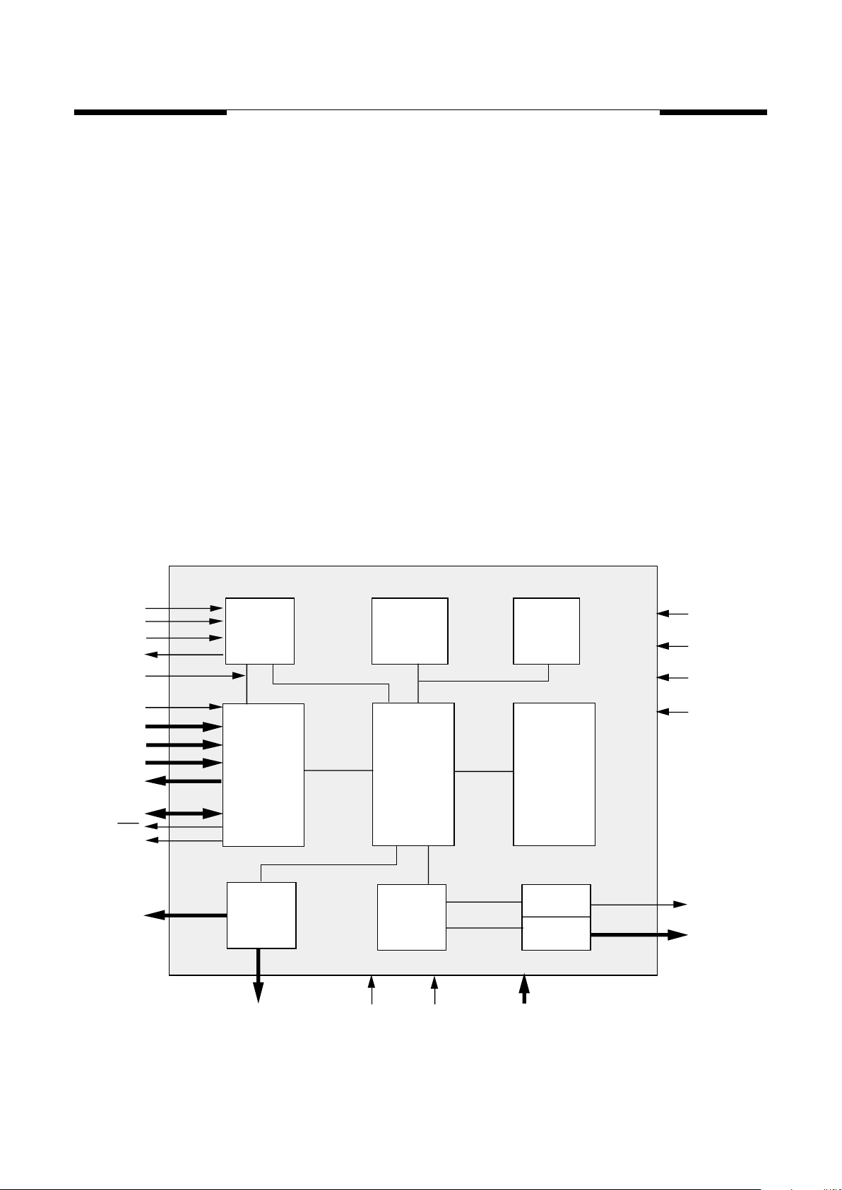
Block Diagram
OSC
C
out
G
eneral Description
The MSu001 is a monolithic talking microcomputer that can memorize voice up to 22 seconds using
MOSEL qualified coding method(MPCM). It's an integration of traditional 4-bit microcomputer and voice
chip with minimal external components. LCD driver and miscellaneous interface are provided for
versatile applications. With more than 10K ROM/RAM inside, this chip meets every intelligent novelty.
Customer requested function and voice data will be built in by changing masks during fabrication.
CAP
X1
X2
TIMER
CIRCUIT
PROGRAM
/DATA
ROM
DATA
RAM
BUZZER
&
LOGICS
CPU
VOICE
DATA
ROM
LCD
DRIVER
MPCM
DECODER
CURRENT
BUFFER
BUZZER
BUFFER
Vout1
Vout2
TEST
TESTA
TESTP
TESTN
RES
VBZ/INT
CUP1,2
S1,2,3,4
M1,2,3,4
P1,2,3,4
IOB3,4
EB2
PWR
COM1-3
SEG1-25 BAK V
dd Vss0-3
February 1996
Page 2
MOSEL VITELIC
MSu001/u001T
PID219D 02/96
2/12
H
ardware Features
Low current consumption
Maximal function with minimal cost
Current output could drive 8 ohm speaker with a
transistor, Vout could drive buzzer directly.
The voice content is stored up to 20 seconds at 6 KHz
S.R. and can be separated up to 64 sections.
22 seconds at 5.51 KHz sample rate (1DA00h)
LCD driver provided, can drive up to 75 segments
Built-In clock generator
Built-In doubler, halver, tripler
Internal program ROM : 1024 x 15 bits;
Internal program RAM : 64 x 4 bits
Two 4-bit input ports
Two 4-bit input/output ports
One 4-bit output port
Development Supports
Development tools are provided
Software / Hardware programming guide is provided
Engineering sample could be provided
S
oftware Features
78 instructions, in 48 categories
4-level subroutine nesting (also used for interrupt)
Two external factors (INT, S&M) for interrupt
Two internal factors (timer, divider) for interrupt
M
ask Options
mask option for either open or hold transistor on S
port & M port
mask option for either pull down or put up on
Interrupt switch
mask option for either leading edge or trailing edge
on Interrupt edge
mask option for either power back-up activated or
not when power on
mask option for either with reset or not when power
on
mask option for either 8 ms or 2 ms chattering
removal time on S port & M port
mask option for either slow (by 15.625 ms) or fast
(by 224.14 us) set time timer
mask option for either fast system clock ( Fosc)
or slow system clock ( Fosc / 2)
LCD display frequency : (1) 128 Hz /170.7 Hz (2)
64Hz /85.3 Hz (3) 32Hz /42.7Hz
LCD driver : (1) static (2) 1/2 bias 1/2 duty (3) 1/2
bias 1/3 duty
A
C Characteristics at 4.5 V & 6 KHz S.R.
Timing
Min. Max.
T
Write Enable pulse width
W
T
Trigger address hold time
H
T
Write Enable to BUSY delay time
WB
T
Write Enable to Audio delay time
WA
300ns
80ns
1 us
500us
Sample Applications
handy game with LCD
versatile timepiece with LCD
talking timer with LCD
intelligent calculator with LCD
smart stationery with LCD
talking home electronics with LCD
T
S
Trigger address setup time
220ns
MSM9058
MSM9012
MSM9011
MSM9009
Developing Card
LCD display emulation board
Program code emulation board
20" (30") Sound emulation board
talking education kit with LCD
Remarks
SRD
SRD
SRD
SRD
SRD
SRD := Sample Rate Dependent
Page 3
MOSEL VITELIC
Pad Descriptions
3/12 PID219D 02/96
1
2
3,4
5
6
7
8,35,34
9-33
38,39,36
37
40,41
42
43
44-47
48
49
50
51
52
53,54
55,56
57,58
59
60-63
64-67
68,69
70,71
Vdd1
Vreg
CUP1,2
X1
X2
CAP
Com1,2,3
SEG1-25
Vss1,2,3
BAK
S4,S3
PWR(alm)
#EB2
TG0,1,2,3
RESET
Vdd2
Rosc
Vss0
Cout
Vout1,2
TG4,5
IOB3,4
VBZ/INT
P1,2,3,4
M1,2,3,4
NC
S2,S1
1
1
2
1
1
1
3
25
3
1
2
1
1
4
1
1
1
1
1
2
2
2
1
4
4
1
2
Power
O
I
I
O
O
O
O
Power
Power
I
I/O
I/O
I/O
I
Power
I
Power
O
O
I/O
I/O
I/O
O
I
NC
I
Positive power supply for CPU function block
Voltage regulator
Voltage doubler capacitor
Crystal Oscillator input, 32768 Hz
Crystal Oscillator Output, 32768 Hz
Phase compensating capacitor
Common plate for LCD panel
25 segment outputs for LCD panel
Negative power supply
BackUp negative power supply
One-way input port; note 1
Pop noise eliminating signal; internally connected to CPU output port
Enable signal to latch section address; internally connected to CPU output port
Trigger address inputs to voice function block; note 2
System reset
Positive supply for voice function block, internally connected to pad 1
Oscillator Resistor for voice function block
Negative power supply for voice signal
Audio signal current output
Audio signal voltage output
Trigger address inputs to voice function block; note 3
Bidirectional input/output port, 2 bits
Busy status output; internally connected to INT (interrupt request) pin of CPU
One-way output port, 4 bits
One-way input port; note 1
No connection
One-way input port, note 1
Note 1. with chatter removal time for either 8 ms (ph8) or 2 ms (ph6)
Note 2. internally connected to CPU I/O port, IOA1=TG0, IOA2=TG1, IOA3=TG2, IOA4=TG3
Note 3. internally connected to CPU I/O port, IOB1=TG4, IOB2=TG5
Pad No. Signal I/O F u n c t i o n s
MSu001/u001T
Vss1
BAK
Vreg
CAP
X1
S1,2,3,4
M1,2,3,4
(IOA1,2,3,4)TG0,1,2,3
IOB1,2,3,4
VBZ/INT
RESET
Rosc
X2
PWR(ALM)
#EB2
P1,2,3,4
SEG1-25
COM1,2,3
CUP1,2
Vout1,2
T(operating)
T(storage)
1.2-1.8
0.0-0.6
0.0-0.6
Vreg-Vd
Vreg-Vdd
Vss-Vdd
Vss-Vdd
Vss-Vdd
Vss-Vdd
Vss-Vdd
Vss-Vdd
Vss-Vdd
Vreg-Vdd
Vss-Vdd
Vss-Vdd
Vss3-Vdd
Vss3-Vdd
Vss3-Vdd
Vss3-Vdd
Vss-Vdd
-60-+60
-55-+125
V
V
V
V
V
V
V
V
V
V
V
V
V
V
V
V
V
V
V
V
Degree C
Degree C
Symbol Rating Unit Symbol Rating Unit
Absolute Maximum Rating
(Vdd=3.0V, Vss=Vss2=0.0V, Vss3=0.0V/-1.5V)
Page 4
MOSEL VITELIC
DC Characteristics at 3.0 Vdd (u001,u001T)
4/12 PID219D 02/96
I sb
I op
I ohv
I oLv
I co
d F/F
d F/F
R osc
R osc
Vdd
Vdd
Vouts
Vouts
Cout
Cout
Rosc
Rosc
Rosc
Rosc
stand by I
operation I
output high I
output low I
cuurent output
frequency stability
frequency variation
oscillation R
oscillation R
-
-
-
-
-
-
-5
-10
-
-
-
-
1
0.2
5
5
2.5
1.5
-
-
1.2
880
1.1
830
-
-
-
-
-
-
5
10
-
-
-
-
uA
mA
mA
mA
mA
mA
%
%
Mohm
kohm
Mohm
kohm
DC Characteristics at 4.5 Vdd (u001, u001T)
I sb
I op
I ohv
I oLv
I co
V ohp
V oLp
V ohw
V oLw
V ohio
V oLio
V ohc
V oLc
V ohg
V oLg
d F/F
d F/F
R isn
R isf
R imn
R imf
R inh
R inL
R ir
R osc
R osc
stand by I
operation I
output high I
output low I
current output
o/p high V
o/p low V
o/p low V
o/p high V
o/p low V
o/p high V
o/p low V
o/p high V
o/p low V
o/p high V
frequency stability
frequency variation
input R when on
input R when off
input R when on
input R when off
input R
input R
input R
oscillation R
oscillation R
Vdd
Vdd
Vouts
Vouts
Cout
Cout
P port
P port
PWR
PWR
i/o port
i/o port
Com
Com
Seg's
Seg's
S port
S port
M port
M port
VBZ,INT
VBZ,INT
RESET
Rosc
Rosc
Rosc
Rosc
-
-
-
-
-
-
*-0.4V
*-0.4V
*-0.4V
*-0.4V
*-0.4V
-5
-10
-
-
-
-
-
-
-
-
-
-
-
1
0.8
12
12
4
2.5
-
-
330
30
30
30
140
3
18
1.2
910
1.1
800
-
-
-
-
-
*+0.4V
*+0.4V
*+0.4V
*+0.4V
*+0.4V
5
10
-
-
-
-
-
-
-
-
-
-
-
uA
mA
mA
mA
mA
mA
V
V
V
V
V
V
V
V
V
V
%
%
kohm
kohm
kohm
kohm
kohm
kohm
kohm
Mohm
kohm
Mohm
kohm
Symbol Name Valid Min. Typ. Max. Unit Remarks
Symbol Name Valid Min. Typ. Max. Unit Remarks
u001
u001T
[Fosc(3.0V)-Fosc(2.7V)]/Fosc(3.0V)
6 KHz S.R., 1.2 Mohm Rosc
S.R.=6000 Hz, u001
S.R.=8000 Hz, u001
S.R.=6000 Hz, u001T
S.R.=8000 Hz, u001T
u001
u001T
I oh = -400 uA
I oL = 400 uA
I oh = -1 mA
I oL = 1 mA
I oh = -100 uA
I oL = 100 uA
I oh = -4 uA
I oL = 4 uA
I oh = -0.4 uA
I oL = 0.4 uA
[Fosc(4.5V)-Fosc(4.0V)]/Fosc(4.5V)
6 KHz S.R., 1.2 Mohm Rosc
pulldown X'tor=on & note 1
pulldown X'tor=off, halt mode & note 1
pulldown X'tor=on & note 1
pulldown X'tor=off, halt mode & note 1
Vss2=0V, Vi=Vdd, VBZ=high
Vss2=0V, Vi=Vdd, VBZ=low
Vss2=0V, Vi=Vdd
S.R.=6000 Hz, u001
S.R.=8000 Hz, u001
S.R.=6000 Hz, u001T
S.R.=8000 Hz, u001T
Note 1. Vss2=0V, Vi=Vss2+0.4V Note 2. *:= Vdd
MSu001/u001T
COM1
COM2
COM2
Alternating Frequency
Static
V
-
32 Hz
1/2 duty
V
V
32 Hz
1/3 duty
V
V
V
43 Hz
Common Plate Usage
Page 5
MOSEL VITELIC
PID219D 02/96
5/12
02 cm 1
MOSEL 001
S4
S1
A4
A2
M4
M2
P4
P2
B4
B2
S3
S2
A3
A1
M3
M1
P3
P1
B3
B1
C7
C6
RESET
C5
C4
C3
C2
C1
C8
COM2
COM3
10P
R1
Q1
E
R1
R2
R2
VR
C7
C6
X1
COM2
COM1
BAK
VSS3
VSS1
VSS2
C5
MSu001/u001T
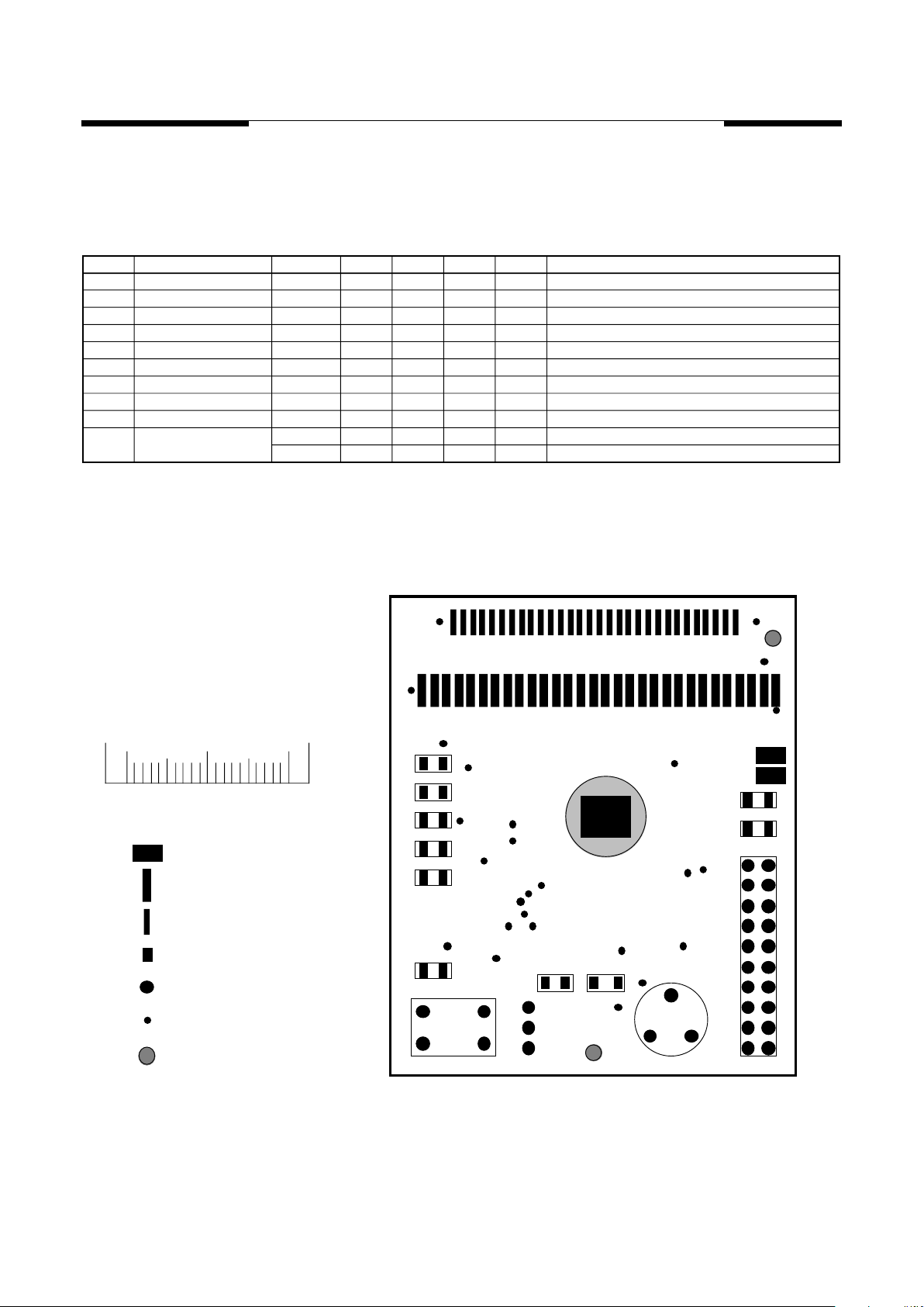
COB Information I
Silk screen & copper print
COB model number : MOSEL 001
Chip bonded : either u001 or u7001
Legend
Copper pad for X'tal
Copper pad for LCD
Copper pad for LCD
Copper pad
Through hole
Through hole
Alignment hole for Jig
DC Characteristics at 3.0 Vdd (u7001)
I sb
I op
I ohv
I oLv
I co
d F/F
d F/F
R is
R im
R osc
Vdd
Vdd
Vouts
Vouts
Cout
S port
M port
Rosc
Rosc
stand by I
operation I
output high I
output low I
cuurent output
frequency stability
frequency variation
input R
input R
oscillation R
-
-
-
-
-
-5
-10
-
-
-
-
300
0.5
7
6
2.5
-
-
-
-
1.2
850
-
-
-
-
5
10
-
-
-
-
uA
mA
mA
mA
mA
%
%
kohm
kohm
Mohm
kohm
Symbol Name Valid Min. Typ. Max. Unit Remarks
[Fosc(3.0V)-Fosc(2.7V)]/Fosc(3.0V)
6 KHz SR, 1.2 Mohm Rosc
S.R.=6000 Hz
S.R.=8000 Hz
Please refer next page for DC characteristics at 4.5V
Page 6

MOSEL VITELIC
PID219D 02/966/12
02 cm 1
MOSEL 001
S4
S1
A4
A2
M4
M2
P4
P2
B4
B2
S3
S2
A3
A1
M3
M1
P3
P1
B3
B1
RESET
C4
C3
C2
C1
C8
E
R1 R2
VR
C7
C6
X1
BAK
C5
CAP
CAP
VSS3
VSS1
VSS2
S4
S3
VDD
VDD
VDD
RESET
VDD
RESET
RESET
ALARM
RESET
C
B
VSS
Cout
RoscVDD
VSS
Cout
Cout
Cout
VSS
VSS
INT
Vout2
Vout1
A1
A2
A3
A4
LIGHT
VPP
VREG
CUP1CUP2
Xout
Xin
CAP
C
O
M
2
C
O
M
3
S
2
5
S
2
4
S
2
3
S
2
2
S
2
1
S
2
0
S
1
9
S
1
8
S
1
7
S
1
6
S
1
5
S
1
4
S
1
3
S
1
2
S
1
1
S
1
0
S9S8S7S6S5S4S3S2S
1
C
O
M
1
COM1
C
O
M
2
COM2
510152025
25 20 15 10
1
15
MSu001/u001T
COB Information II
Signal Name & Location Description
COB model number : MOSEL 001
Chip bonded : either u001 or u7001
Please refer previous page for legends
DC Characteristics at 4.5 Vdd (u7001)
I sb
I op
I ohv
I oLv
I co
d F/F
d F/F
R is
R im
R osc
stand by I
operation I
output high I
output low I
current output
frequency stability
frequency variation
input R
input R
oscillation R
Vdd
Vdd
Vouts
Vouts
Cout
S port
M port
Rosc
Rosc
-
-
-
-
-
-5
-10
-
-
-
-
900
1.0
16
12
4
-
140
150
1.2
880
-
-
-
-
5
10
-
-
-
-
uA
mA
mA
mA
mA
%
%
kohm
kohm
Mohm
kohm
Symbol Name Valid Min. Typ. Max. Unit Remarks
[Fosc(4.5V)-Fosc(V-0.5)]/Fosc(4.5V)
6 KHz S.R., 1.2 Mohm Rosc
Vss2=0V, Vi=Vss2+0.4, halt mode
Vss2=0V, Vi=Vss2+0.4, open mode
S.R.=6000 Hz
S.R.=8000 Hz
Please refer to previous page for Characteristics at 3.0 V
Page 7

MOSEL VITELIC
MSu001/u001T
7/12 PID219D 02/96
Timing Diagram
I. Addressing 6 - bit
AUDIO
BUSY
EB2
TG5(IOB2)
Low
TG4(IOB1)
Low
TG3(IOA4)
TG2(IOA3)
TG1(IOA2)
TG0(IOA1)
S06
S09
AUDIO
BUSY
II. PWR Signal
PWR
T
WB
T
WA
T
H
T
W
One portion of the program to play a sound
CLRM 4h ; #EB2 Low
OUT PA , R5 ;
OUT PB , R6 ;
SETM 4h ; #EB2 High
1. When PWR is high , MSu001 audio output signal will stay at approx. 2.4V even there is no audio output .
2. When PWR is low , MSu001 audio output signal will stay at GND level when there is no audio output .
3. For eliminating the "pop" noise purpose , PWR should be at high level when a sound section is played
over , and also at high level in between two sound sections .
4. For energy saving purpose , PWR should not always stay at high level , since there will be a hundred-mA
current consumption when PWR is high . So it should go to low level when its not needed .
T
S
S
tandardCode LineUp
MSSu001-066 Mandarin talking watch/clock
MSSu001-068 English talking watch/clock
MSSu001-078 Russian talking calculator
MSSu001-090 Mandarin talking calculator
Page 8

MOSEL VITELIC
MSu001/u001T
8/12 PID219D 02/96
Bonding Diagram
Designation
VDD
VREG
CUP1
CUP2
X1
X2
CAP
COM1
SEG1
SEG2
SEG3
SEG4
Pad No.
1
2
3
4
5
6
7
8
9
10
11
12
XY
Designation
SEG5
SEG6
SEG7
SEG8
SEG9
SEG10
SEG11
SEG12
SEG13
SEG14
SEG15
SEG16
Pad No.
13
14
15
16
17
18
19
20
21
22
23
24
XY
Designation
SEG17
SEG18
SEG19
SEG20
SEG21
SEG22
SEG23
SEG24
SEG25
COM3
COM2
VSS3
Pad No.
25
26
27
28
29
30
31
32
33
34
35
36
XY
Designation
BAK
VSS1
VSS2
S4
S3
PWR(ALM)
EB2 (LIGHT)
TG0(IOA1)
TG1(IOA2)
TG2(IOA3)
TG3(IOA4)
RESET
Pad No.
37
38
39
40
41
42
43
44
45
46
47
48
XY
Designation
VDD
OSC
VSS0
COUT
VOUT1
VOUT2
TG4(IOB1)
TG5(IOB2)
IOB3
IOB4
VBZ/INT
P1
Pad No.
49
50
51
52
53
54
55
56
57
58
59
60
XY
Designation
P2
P3
P4
M1
M2
M3
M4
NC
NC
S2
S1
Pad No.
61
62
63
64
65
66
67
68
69
70
71
XY
-1443.1
-1263.1
- 903.1
- 723.1
- 543.1
- 363.1
- 183.1
- 3.1
176.9
356.9
536.9
-1083.1
-1639.5
-1639.5
-1639.5
-1639.5
-1639.5
-1639.5
-1639.5
-1639.5
-1639.5
-1639.5
-1639.5
-1639.5
-1983.1
-1983.1
-1983.1
-1983.1
-1983.1
-1983.1
-1983.1
-1983.1
-1983.1
-1983.1
-1983.1
-1983.1
325.2
145.2
- 34.8
- 214.8
- 394.8
- 665.1
-1033.7
-1261.4
-1459.4
-1639.5
-1639.5
-1639.5
716.9
896.9
1256.9
1436.9
1616.9
1796.9
1976.9
1983.9
1983.9
1983.9
1947.1
1076.9
-1639.5
-1639.5
-1639.5
-1639.5
-1639.5
-1639.5
-1639.5
-1459.5
-1279.3
-1036.3
- 856.3
-1639.5
1947.1
1937.1
-1983.1
-1983.1
-1983.1
-1983.1
-1983.1
-1983.1
-1983.1
-1983.1
-1983.1
-1983.1
- 676.3
- 496.3
- 316.3
- 136.3
43.7
223.7
403.7
583.7
763.7
943.7
1303.7
1123.7
1941.2*
1588.6
1370
1151.4
524.5
122.1
- 98.2
- 278.2
- 458.2
- 638.2
- 998.2
- 818.2
1637.8
1636.1
1630.6
1611.4
1612.3
1612.3
1642.9
1642.9
1642.9
1642.9
1642.9
1642.9
-1178.2
-1358.2
-1538.2
-1718.2
-1983.1
-1898.2
1642.9
1642.9
1642.9
1642.9
1405.2
1642.9
1225.2
1045.2
865.2
685.2
-1983.1
-1983.1
-1983.1
-1983.1
-1983.1 505.2
Page 9

MOSEL VITELIC
9/12
PID219D 02/96
MSu001/u001T
Application Circuit
1
2
3
4
5
6
8
9
11 1213 14 1516 17 2122 23 24
27
28 30
31
34
35
36
37
38
39
40
41
42
43
44
45
46
47
48
5152535455565758596061626364
66
67
68
69
71
70
7
1819 20 25 26
29
Substrate is Vdd
4290 x 3670 um
Pad size : 90 x 90 um
Rosc
P1
P2
P3
P4
VBZ/INT
T
G
4
Buzzer
VSS0
RES
TG3
TG2
TG1
TG0
EB2
PWR
S3
S4
VSS2
VSS1
BAK
VSS3
COM2
COM3
SEG25
SEG25
COM3
COM2
SEG16SEG8SEG1
COM1
COM1
SEG1
CAP
X2
32768Hz
CUP1
S1
S2
M4
LCD (1/3 duty , 1/2 bias)
Note:
1. T(transistor) = ß > 150, R2=470Ω ,S(speaker) = 1/4 w, 8 Ω; all typical.
2. R2=470Ω ( typical ) to bypass extra current into base to get rid of waveform saturation on collector .
3. Piezo buzzer resonant frequency is around 1K Hz.
4. All the above components need to adjust possibly case by case to meet required performance.
5. Vout1,Vout2 are tristate during stand by.
+
-
R2
CUP2
X1
0.1u
0.1u
0.1u
VDD
0.1u
M3 M2 M1
T
G
5
Vout1
Vout2
Reset
Taiwan
#1, Creation Road I,
Science-based Industrial Park,
Hsinchu 30077
Taiwan, ROC
"taylor_hsiao@ccmail.mosel.com.tw"
TEL: 886-35-770055
FAX: 886-35-772788
FAX: 886-35-784732
Taipei
7F, #102 Section 3,
Ming Chung East Road,
Taipei,
Taiwan, ROC
TEL: 886-2-5451213
FAX: 886-2-5451214
Hongkong
#19 Dai Fu Street,
Taipo Industrial Estate,
Taipo, N.T.
Hongkong
TEL: 852-2388-8277
TEL: 852-2665-4883
FAX: 852-2664-2406
FAX: 852-2770-8011
U.S.A.
#3910 North First Street,
San Jose,
CA.65134-1501
U.S.A.
TEL: 1-408-433-6000
FAX: 1-408-433-0952
MSµ001
Page 10

MOSEL VITELIC
Product Request Form
10/12 PID219D 02/96
Customer
Agent
Sales
Represen.
Sound
Providing
to
MVI
Code
Providing
to MVI
Serviced
Required
from
MVI
Who is MVI sales you contact ?
8-bit PCM sound files
.WAV sound files
DAT or equivalent
Something special in written memo
Others
.TRA program file, name =
.EVA LCD file, name =
.HEX program file, name =
.HEX LCD file, name =
EPROMs with data inside
files to pro'med into EPROM
9011 & 9012 emulation boards
u7001 chip on board
Confirm table
Others
Buzzer (F fr= 1K Hz)
Speaker (8 ohm, 1" diam)
Other
2.5 V
3.0 V
3.5 V
4.0 V
4.5 V
5.0 V
5.5 V
6.0 V
Battery size "D"
Battery size "AA"
Battery size "AAA"
Battery button cell
Mains
Other
T i t l e
SampleRate
Output
Device
Working
Voltage
Power
Source
General Descriptions Chip Descriptions
Hz
Company Name :
Signature :
Position Title :
Department, Section :
Signature Date :
Mosel Vitelic Inc.
886-35-772788 (fax)
Sales & Marketing Department
We hereby request MVI to start preparing produce MSSu001 which is specified as
I already read this data sheet and understand MSu001 completely and know how to
below descriptions as well as form A and form B.
specify to fit my requirement.
T O :
Attention :
MSu001/u001T
Page 11

MOSEL VITELIC
Product Request Form A : Voice Word Definitions : There are words defined.
1< <6 4
11/12 PID219D 02/96
T I T L E
00
01
02
03
04
05
06
07
08
09
10
11
12
13
14
15
16
17
18
19
20
21
22
23
24
25
26
27
28
29
30
31
32
33
34
35
36
37
38
39
40
41
42
43
44
45
46
47
48
49
50
51
52
53
54
55
56
57
58
59
60
61
62
63
00h
00h
00h
00h
00h
00h
00h
00h
00h
00h
00h
00h
00h
00h
00h
00h
00h
00h
00h
00h
00h
00h
00h
00h
00h
00h
00h
00h
00h
00h
00h
00h
00h
00h
00h
00h
00h
00h
00h
00h
00h
00h
00h
00h
00h
00h
00h
00h
00h
00h
00h
00h
00h
00h
00h
00h
00h
00h
00h
00h
00h
00h
00h
00h
00h
00h
00h
00h
00h
00h
00h
00h
00h
00h
00h
00h
00h
00h
00h
00h
00h
00h
00h
00h
00h
00h
00h
00h
00h
00h
00h
00h
00h
00h
00h
00h
00h
00h
00h
Length summ. of above 64 words
must be
< 1DA00h00h
00h
00h
00h
00h
00h
00h
00h
00h
00h
00h
00h
00h
00h
00h
00h
00h
00h
00h
00h
00h
00h
00h
00h
00h
00h
00h
00h
00h
00h
00h
00h
00h
00h
00h
00h
00h
00h
00h
00h
00h
00h
00h
00h
00h
00h
00h
00h
00h
00h
00h
00h
00h
00h
00h
00h
00h
00h
00h
00h
00h
00h
00h
00h
00h
00h
00h
00h
00h
00h
00h
00h
00h
00h
00h
00h
00h
00h
00h
00h
00h
00h
00h
00h
00h
00h
00h
00h
00h
00h
00h
00h
00h
00h
Voice Description VoiceLength MuteLength
WordTotal
< 80000h
Address
Signature & date
MVI Sales & date
S
S
S
S
S
S
S
S
S
S
S
S
S
S
S
S
S
S
S
S
S
S
S
S
S
S
S
S
S
S
S
S
S
S
S
S
S
S
S
S
S
S
S
S
S
S
S
S
S
S
S
S
S
S
S
S
S
S
S
S
S
S
S
S
S
S
S
S
S
S
S
S
S
S
S
S
S
S
S
S
S
S
S
S
S
S
S
S
S
S
S
S
S
S
S
S
S
S
S
S
S
S
S
S
S
S
S
S
S
S
S
S
S
S
S
S
S
S
S
S
S
S
S
S
S
S
S
S
00h
01h
02h
03h
04h
05h
06h
07h
08h
09h
0Ah
0Bh
0Ch
0Dh
0Eh
0Fh
10h
11h
12h
13h
14h
15h
16h
17h
18h
19h
1Ah
1Bh
1Ch
1Dh
1Eh
1Fh
20h
21h
22h
23h
24h
25h
26h
27h
28h
29h
2Ah
2Bh
2Ch
2Dh
2Eh
2Fh
30h
31h
32h
33h
34h
35h
36h
37h
38h
39h
3Ah
3Bh
3Ch
3Dh
3Eh
3Fh
MSu001/u001T
Page 12

MOSEL VITELIC
Product Request Form B : Mask Definitions
PID219D 02/96
T I T L E
Signature & date
MVI sales & date
Power bias
LCD driver &
display frequency
S-port defined
M-port defined
Interrupt switch
Interrupt edge
Power-on mode
External Reset
Chatter Removal time
Set time
Oscillator
System Clock
Alarm frequency
P-port
Input port signal
Light mode
Reset level
I/O port
Light
Li - 1/2 Bias
1/2 duty 128 Hz
1/3 duty 170.7 Hz
Static 128 Hz
Open
Open
Pull down
Rising
BackUp
and PowerOn reset
8 mS time
Slower (Tk=512 mS)
Crystal
Fast (Fosc)
Level shift
Level shift
Level shift
Always
High
Level shift
Level shift
1/2 duty 64 Hz
1/3 duty 85.3 Hz
Static 64 Hz
Hold transistor
Hold transistor
Pull up
Falling
Non-BackUp
Only
2 mS time
Faster (Tk=8000uS)
Slow (Fosc/2)
1/2 duty 32 Hz
1/3 duty 42.7 Hz
Static 32 Hz
1
2
3
4
5
6
7
8
9
10
11
12
13
14
15
16
17
18
19
Mask options S e l e c t i o n s
V
V
V
V
V
V
V
V
V
note
note
note
Note 9 : For S port and M port
Note 10 : Set time = (set value + 1) * Tk / Fosc ; Fosc is in KHz
Note 15 : Input port control signal level shift, J48, J49
MSu001/u001T
12/12
 Loading...