

Page 1
PRELIMINARY DATA SHEET
MICRONAS
MSP 44x8G
Multistandard
Sound Processor
Edition Feb. 25, 2000
6251-516-1PD
MICRONAS
Page 2

MSP 44x8G PRELIMINARY DATA SHEET
Contents
Page Section Title
5 1. Introduction
6 1.1. Features of the MSP 44x8G Family
6 1.2. MSP 44x8G Version List
7 1.3. MSP 44x8G Versions and their Application Fields
8 2. Functional Description
8 2.1. Architecture of the MSP 44x8G Family
9 2.2. MSP 44x8G Sound IF Processing
9 2.2.1. Analog Sound IF Input
9 2.2.2. Demodulator: Standards and Features
9 2.2.3. Preprocessing of Demodulator Signals
10 2.2.4. Automatic Sound Select
10 2.2.5. Manual Mode
2
12 2.3. Preprocessing for SCART and I
12 2.4. Source Selection and Output Channel Matrix
12 2.4.1. Mixing Unit
12 2.5. Audio Baseband Processing
12 2.5.1. Automatic Volume Correction (AVC)
13 2.5.2. Main and Aux Outputs
13 2.5.3. Quasi-Peak Detector
13 2.6. SCART Signal Routing
13 2.6.1. SCART DSP In and SCART Out Select
13 2.6.2. Stand-by Mode
2
13 2.7. I
13 2.7.1. Synchronous I
13 2.7.2. Asynchronous I
S Bus Interfaces
2
S-Interface(s)
2
S-Interface
14 2.8. ADR Bus Interface
14 2.9. Digital Control I/O Pins and Status Change Indication
14 2.10. Preemphasis
14 2.11. Clock PLL Oscillator and Crystal Specifications
S Input Signals
15 3. Control Interface
2
15 3.1. I
C Bus Interface
15 3.1.1. Device and Subaddresses
16 3.1.2. Description of CONTROL Register
16 3.1.3. Protocol Description
2
17 3.1.4. Proposals for General MSP 44x8G I
C Telegrams
17 3.1.4.1. Symbols
17 3.1.4.2. Write Telegrams
17 3.1.4.3. Read Telegrams
17 3.1.4.4. Examples
2
17 3.2. Start-Up Sequence: Power-Up and I
C Controlling
17 3.3. MSP 44x8G Programming Interface
17 3.3.1. User Regi sters Overview
20 3.3.2. Description of User Registers
21 3.3.2.1. STANDARD SELECT Register
21 3.3.2.2. STANDARD RESULT Register
2 Micronas
Page 3

PRELIMINARY DATA SHEET
Contents, continued
Page Section Title
MSP 44x8G
22 3.3.2.3. Write Registers on I2C Subaddress 10
25 3.3.2.4. Read Registers on I2C Subaddress 11
26 3.3.2.5. Write Registers on I2C Subaddress 12
33 3.3.2.6. Read Registers on I2C Subaddress 13
hex
hex
hex
hex
34 3.4. Programming Tips
34 3.5. Examples of Minimum Initialization Codes
34 3.5.1. B/G-FM (A2 or NICAM)
34 3.5.2. BTSC-Stereo
34 3.5.3. BTSC-SAP with SAP at Main Channel
35 3.5.4. FM-Stereo Radio
35 3.5.5. Automatic Standard Detection
35 3.5.6. Software Flow for Interrupt driven STATUS Check
37 4. Specifications
37 4.1. Outline Dimensions
39 4.2. Pin Connections and Short Descriptions
42 4.3. Pin Descriptions
45 4.4. Pin Configurations
48 4.5. Pin Circuits
50 4.6. Electrical Characteristics
50 4.6.1. Absolute Maximum Ratings
51 4.6.2. Recommended Operating Conditions (T
= 0 to 70 °C)
A
51 4.6.2.1. General Recommended Operating Conditions
51 4.6.2.2. Analog Input and Output Recommendations
52 4.6.2.3. Recommendations for Analog Sound IF Input Signal
53 4.6.2.4. Crystal Recommendations
54 4.6.3. Characteristics
54 4.6.3.1. General Characteristic s
55 4.6.3.2. Digital Inputs, Digital Outputs
56 4.6.3.3. Reset Input and Power-Up
2
57 4.6.3.4. I
58 4.6.3.5. I
C-Bus Characteristics
2
S-Bus Characteristics
60 4.6.3.6. Analog Baseband Inputs and Outputs, AGNDC
62 4.6.3.7. Sound IF Inputs
62 4.6.3.8. Power Supply Rejection
63 4.6.3.9. Analog Performance
66 4.6.3.10. Sound Standard Dependent Characteristics
69 5. Appendix A: Overview of TV-Sound Standards
69 5.1. NICAM 728
70 5.2. A2-Systems
71 5.3. BTSC-Sound System
71 5.4. Japanese FM Stereo System (EIA-J)
72 5.5. FM Satellite Sound
72 5.6. FM-Stereo Radio
Micronas 3
Page 4

MSP 44x8G PRELIMINARY DATA SHEET
Contents, continued
Page Section Title
73 6. Appendix B: Manual Mode
73 6.1. Demodulator Write and Read Registers for Manual Mode
74 6.2. DSP Write and Read Registers for Manual Mode
74 6.3. Manual Mode: Description of Demodulator Write Registers
74 6.3.1. Automatic Switching between NICAM and Analog Sound
74 6.3.1.1. Function in Automatic Sound Select Mode
75 6.3.1.2. Function in Manual Mode
76 6.3.2. A2 Threshold
76 6.3.3. Carrier-Mute Threshold
77 6.3.4. DCO-Registers
77 6.4. Manual Mode: Description of Demodulator Read Registers
78 6.4.1. NICAM Mode Control/Additional Data Bits Register
78 6.4.2. Additional Data Bits Register
78 6.4.3. CIB Bits Register
78 6.4.4. NICAM Error Rate Register
79 6.5. Manual Mode: Description of DSP Write Registers
79 6.5.1. Additional Channel Matrix Modes
79 6.5.2. FM Fixed Deemphasis
79 6.5.3. FM Adaptive Deemphasis
79 6.5.4. NICAM Deemphasis
79 6.5.5. Identification Mode for A2 Stereo Systems
80 6.6. Manual Mode: Description of DSP Read Registers
80 6.6.1. Stereo Detection Register for A2 Stereo Systems
80 6.6.2. DC Level Register
80 6.7. Demodulator Source Channels in Manual Mode
80 6.7.1. Terrestrial Sound Standards
80 6.7.2. SAT Sound Standards
82 7. Appendix C: Application Information
82 7.1. Exclusions of Audio Baseband Features
82 7.2. Phase Relationship of Analog Outputs
83 7.3. Application Circuit
84 8. Data Sheet History
4 Micronas
Page 5
PRELIMINARY DATA SHEET MSP 44x8G
Multistandard Sound Processor Family
1. Introduction
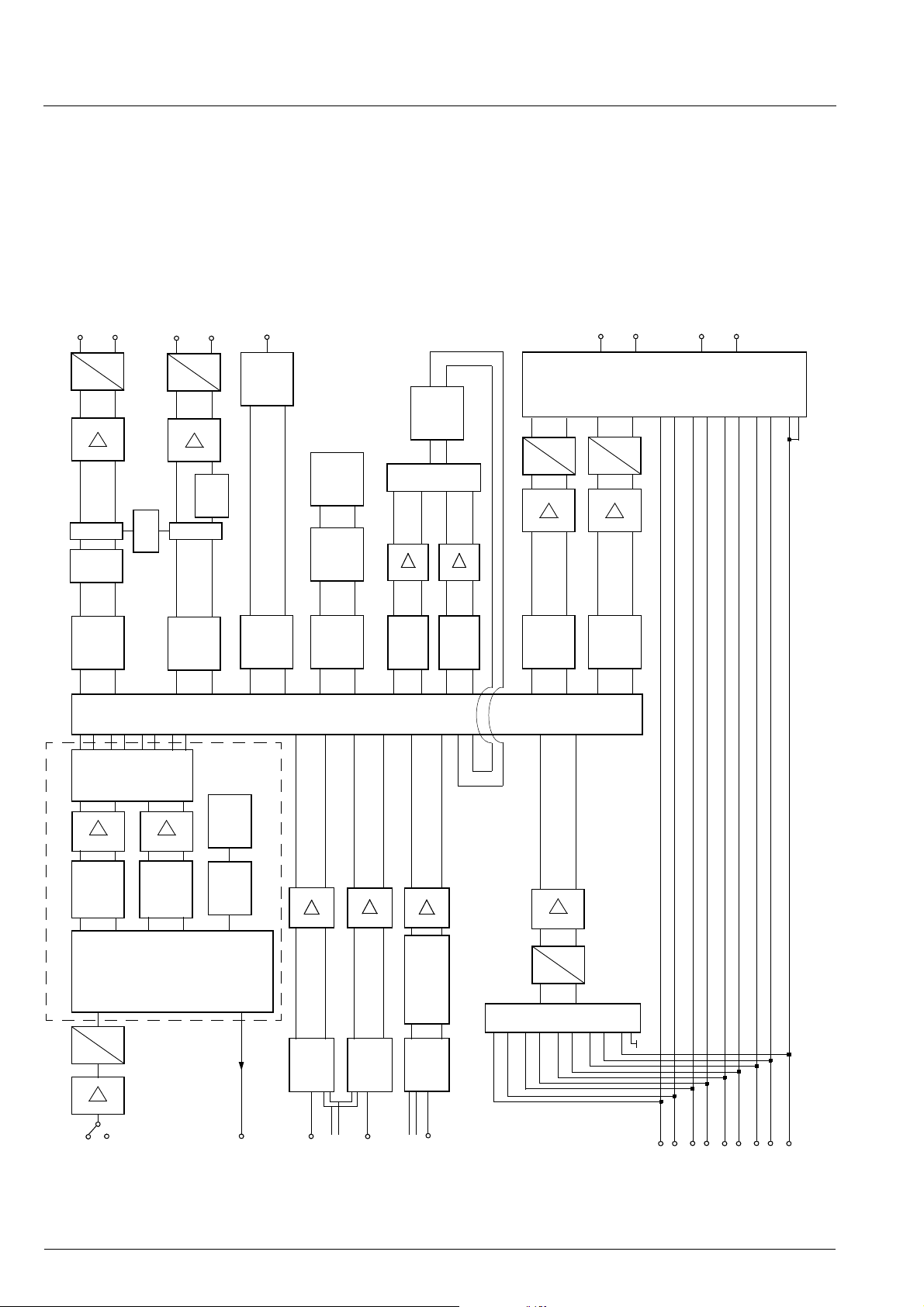
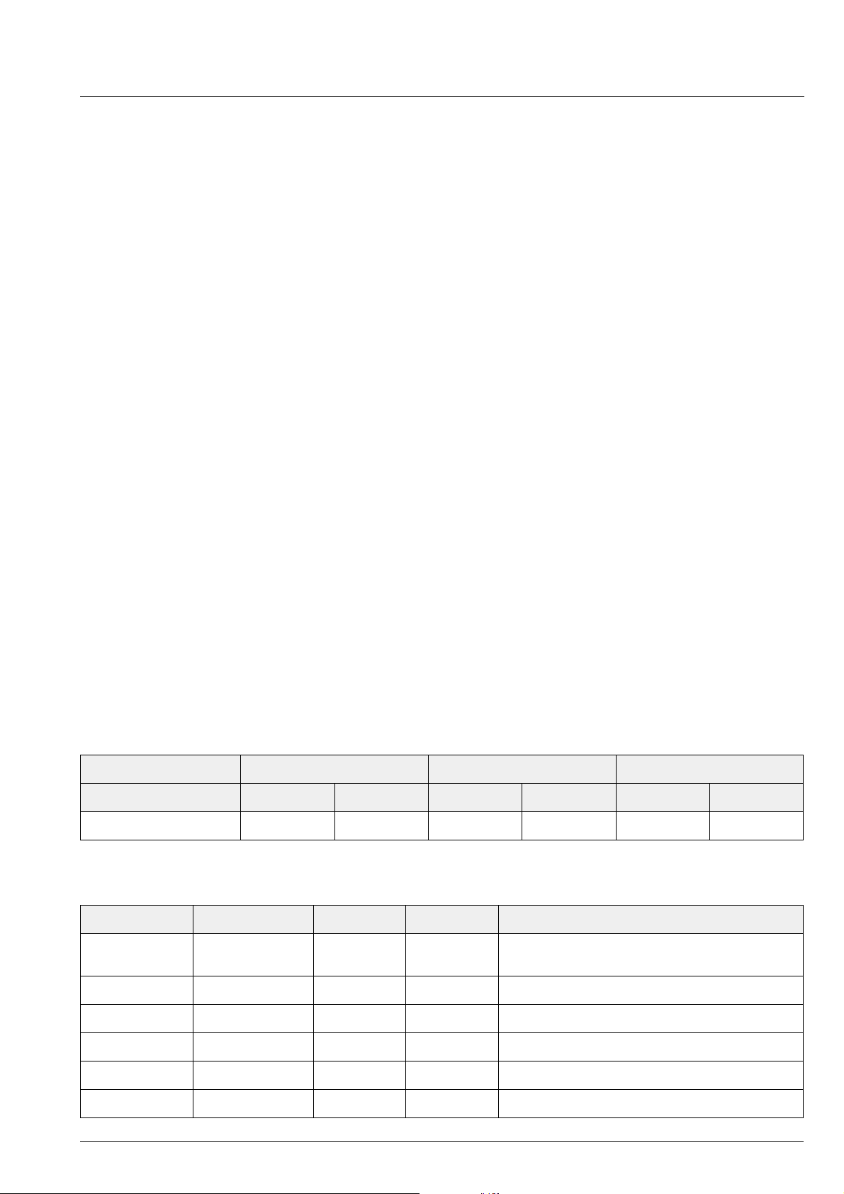
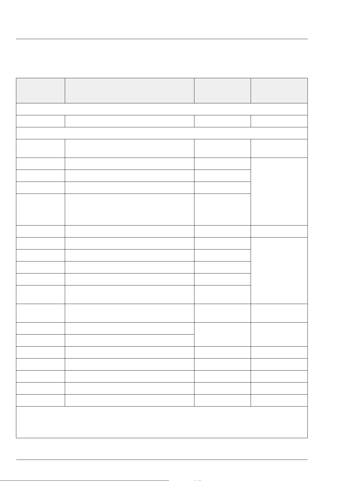
The MSP 44x8G family of Multistandard Sound Processors covers the soun d proce ssi ng of a ll anal og T VStandards worldwide, as well as the NICAM digital
sound standards. The fu ll TV so und processing , star ting with analog sound IF signa l-in, down to process ed
analog AF-out, is perform ed on a single chi p. Fig. 1–1
shows a simplified functional block diagram of the
MSP 44x8G.
The high-quality A /D and D/A converters offer the full
audio bandwidth of 20 kHz and the backend DSP processing is performed at a 48 kHz sample rate.
The MSP 44x 8G has been designed for the usage in
hybrid set-top boxes and multimedia applications. Its
asynchronous I
2
S slave interface allows the recepti on
of digital stereo signals with arbitrary sample rates
ranging from 5 to 50 kHz. Synchronization is performed by means of an adaptive sample rate converter.
This generation of TV soun d processing ICs includes
versions for processing the multichannel television
sound (MTS) signal conforming to the standard recommended by the Broadcast Television Systems Committee (BTSC). The DBX noise red uction, or alter nati vely,
Micronas Noise Reductio n (MNR) is performed alignment free.
Other processed s tandards are the Japanese FM-FM
multiplex standard (EIA-J) and the FM Stereo Radio
standard.
The MSP 44x 8G versions are pin and software compatible to other MSP families. Standard selection
requires only a single I
2
C transmission.
The MSP 44x8G has built-in automatic functions: The
IC is able to detect the actual sound standard automatically (Automatic Standard Detection). Furthermore,
pilot levels and identification sign als can be evaluated
internally with subsequent switching between mono/
stereo/bilingual; no I
2
C interaction is ne cessar y (Auto-
matic Sound Selection).
The ICs are produced in submicron CMOS technology
and are available in the following packages: PQFP 80,
PLQFP64, and PSDIP64.
Sound IF1
Sound IF2
I2S1
I2S2
I2S3
SCART1
SCART2
SCART3
SCART4
MONO
ADC
synchron.
2
I
S
asychron.
2
S
I
SCART
DSP
Input
Select
De-
modulator
ADC
Pre-
processing
Prescale
Prescale
Fig. 1–1: Simplified functional block diagram of the MSP 44x8G
Main
Sound
Processing
Aux
Sound
Processing
Source Select
DAC
DAC
DAC
DAC
DAC
SCART
Output
Select
Main
Channel
Aux
Channel
I2S
SCART1
SCART2
Micronas 5
Page 6
MSP 44x8G PRELIMINARY DATA SHEET
1.1. Features of the MSP 44x8G Family
Feature 4408 4418 4428 4448 4458
2
Standard Selection with single I
Automatic Standard Detection of terrestrial TV standards X X X X X
Automatic Sound Selection (mono/stereo/bilingual), new registers MODUS, STATUS X X X X X
Two selectable sound IF (SIF) inputs X X X X X
Automatic Carrier Mute function X X X X X
Interrupt output programmable (indicating status change) X X X X X
Main/Aux channel with volume, balance, bass, treble, loudness X X X X X
AVC: Automatic Volume Correction X X X X X
Two channel mixer XXXXX
Selectable preemphasis for Aux channel X X X X X
Four Stereo SCART (line) inputs, one Mono input; two Stereo SCART outputs X X X X X
Complete SCART in/out switching matrix X X X X X
2
Two 48kHz I
S inputs; one ansynchronous 5..50 kHz I2S input, one 48 kHz I2S output X X X X X
C transmission X X X X X
All analog FM-Stereo A2 and satellite standards; AM-SECAM L standard X X X
Simultaneous demodulation of (very) high-deviation FM-Mono and NICAM X X
Adaptive deemphasis for satellite (Wegener-Panda, acc. to ASTRA specification) X X X
ASTRA Digital Radio (ADR) together with DRP 3510A X X X
All NICAM standards XX
Demodulation of the BTSC multiplex signal and the SAP channel X X X
Alignment free digital DBX noise reduction for BTSC Stereo and SAP X X
Alignment free digital Micronas Noise Reduction (MNR) for BTSC Stereo and SAP X
BTSC stereo and EIA-J separation significantly better than spec. X X X
SAP and stereo detection for BTSC system XXX
Korean FM-Stereo A2 standard X X X X X
Alignment-free Japanese standard EIA-J XXX
Demodulation of the FM-Radio multiplex signal X X X
1.2. MSP 44x8G Version List
Version Status Description
MSP 4408G planned FM Stereo (A2) Version
MSP 4418G planned NICAM and FM Stereo (A2) Version
MSP 4428G planned NTSC Version (A2 Korea, BTSC with Micronas Noise Reduction (MNR), and Japanese EIA-J system)
MSP 4448G planned NTSC Version (A2 Korea, BTSC with DBX noise reduction, and Japanese EIA-J system)
MSP 4458G available Global Version (all sound standards)
6 Micronas
Page 7
PRELIMINARY DATA SHEET MSP 44x8G
1.3. MSP 44x8G Versions and their Application Fields
Table 1–1 provides an overview of TV sound standards
that can be processed by the MSP 44x8G family. In
addition, the MSP 44x8G is able to handle the terrestrial FM-Radio stand ard. W ith the MSP 44x8G, a com-
plete multimedia r eceiver covering all TV sound standards together with terrestrial and satellite radio sound
can be built; even ASTRA Digital Radio can be processed (with a DRP 3510A coprocessor).
Table 1–1: TV Stereo Sound Standards covered by the MSP 44x8G Family (details see Appendix A)
MSP Version System Position of Sound
4408
4418
4408
B/G
L 6.5/5.85 AM-Mono/NICAM SECAM-L France
I 6.0/6.552 FM-Mono/NICAM PAL UK, Hong Kong
D/K
4458
Satellite
Carrier / MHz
5.5/5.7421875 FM-Stereo (A2) PAL Germany
5.5/5.85 FM-Mono/NICAM PAL Scandinavia, Spain
6.5/5.85 FM-Mono/NICAM PAL China, Hungary
6.5/6.2578125 FM-Stereo (A2, D/K1) SECAM-East Slovak. Rep.
6.5/6.7421875 FM-Stereo (A2, D/K2) PAL currently no broadcast
6.5/5.7421875 FM-Stereo (A2, D/K3) SECAM-East Poland
6.5
7.02/7.2
7.38/7.56
etc.
Sound
Modulation
FM-Mono
FM-Stereo
ASTRA Digital Radio (ADR)
with DRP 3510A
Color
System
PAL
Broadcast e.g. in:
Europe Sat.
ASTRA
4428/48
Tuner
4.5/4.724212 FM-Stereo (A2) NTSC Korea
M
FM-Radio 10.7 FM-Stereo Radio USA, Europe
SAW Filter
Vision
Demodulator
COMPOSITE
Video
4.5 FM-FM (EIA-J) NTSC Japan
4.5 BTSC-Stereo + SAP NTSC USA
33 34 39MHz 4.5 9MHz
Sound
IF
Mixer
1
2
2
2
2
MSP 44x8G
2
2
SCART1
SCART2
SCART
Inputs
Mono
SCART1
SCART2
SCART3
SCART4
Main
Channel
Aux
Channel
Aux
Channel/
FM-Modulator
SCART
Outputs
I2S3
DolbyDigital/
MPEG
ADR
Digital
Signal
I2S2I2S1
ADR
Decoder
Fig. 1–2: Typical MSP 44x8G application
Micronas 7
Page 8
MSP 44x8G PRELIMINARY DATA SHEET
2. Functional Description
2.1. Architecture of the MSP 44x8G Family
Fig. 2–1 shows a simplified block diagram of the IC.
The block diagram contains all features of the
AVC
DACM_L
DACM_R
A
D
)
(00
Volume
Σ
)
hex
(29
AVC*
)
hex
(08
DACA_L
DACA_R
A
D
hex
Volume
)
hex
(14
Beeper
phasis
Preem-
Σ
)
hex
(09
I2S_DA_OUT
(sync. 48 kHz)
S
2
I
Interface
)
hex
(06
)
hex
(34
)
hex
(0B
*
location is
programmable
Note:
C
2
I
Read
Register
)
(0C
Mix1
hex
Detector
Quasi-Peak
MSP 4458G. Other members of the MSP 44x8G family
do not have the complete set of features, handling only
a subset of the standards (see dashed block in
Fig. 2–1).
)
hex
(3A
scale
)
hex
(38
SC1_OUT_R
SC1_OUT_L
)
hex
(29
AVC*
Σ
)
hex
(3B
Mix2
scale
)
hex
(39
SCART1_L/R
D
Volume
SCART2_L/R
A
A
D
)
hex
(07
)
hex
(40
Volume
)
hex
(0A
)
hex
(41
SC2_OUT_R
SC2_OUT_L
)
hex
SCART Output Select
(13
S
2
Main
Matrix
Channel
Aux
Matrix
Channel
I
Matrix
Channel
Matrix
Channel
Quasi-Peak
Mix1
Channel
Mix2
Matrix
Channel
Matrix
Matrix
Channel
SCART1
Matrix
Channel
SCART2
Source Select
0
1
3
4
5
6
7
15
2
FM/AM
Stereo or A
Stereo or A
Automatic
Soundselect
FM/AM
Deemphasis:
)
hex
(0E
Prescale
Panda1
50/75 µs
DBX/MNR
Stereo or B
)
C
hex
2
I
Read
(10
Standard
and Sound
Register
Detection
)
hex
(16
S1
2
I
Prescale
)
hex
(12
S2
2
I
Prescale
)
hex
(11
S3
2
I
Prescale
)
hex
(0D
SCART
Prescale
NICAM
Prescale
J17
Deemphasis:
D
A
)
SCART DSP Input Select
hex
(13
DEMODULATOR
A2
AM
SAT
EIA-J
BTSC
NICAM
Decoded
Standards:
(incl. Carrier Mute)
FM-Radio
Interpolation
Synchronization /
D
A
S
2
I
Interface
S
2
I
Interface
S
2
I
Interface
AGC
I2S_CL
I2S_WS
ANA_IN2+
ANA_IN1+
Interface
ADR-Bus
I2S_DA_IN1
(sync. 48 kHz)
I2S_DA_IN2
(sync. 48 kHz)
I2S_CL3
I2S_WS3
I2S_DA_IN3
(async. 5-50 kHz)
SC2_IN_L
SC1_IN_L
SC2_IN_R
SC1_IN_R
SC4_IN_L
SC3_IN_L
SC3_IN_R
MONO_IN
SC4_IN_R
8 Micronas
Fig. 2–1: Signal flow block diagram of the MSP 44x8G (input and output names correspond to pin names).
Page 9

PRELIMINARY DATA SHEET MSP 44x8G
2.2. MSP 44x8G Sound IF Processing
2.2.1. Analog Sound IF Input
The input pins ANA_IN1+, ANA_IN2+, and ANA_IN
offer the possibility to conn ect two different sound IF
(SIF) sources to the MSP 44x8G. The preselected
sound IF signal is fed into an A/D-converter. An analog
automatic gain circuit (AG C) allows a wide range of
input levels. The highpass filters, formed by the coupling capacitors at pins ANA_IN1+ and ANA_IN2+
(see Section 7.3. “Application Circuit” on page 83), are
sufficient in most cases to suppress video components. Some combinations of SAW filters and sound IF
mixer ICs, however, show large picture components on
their outputs. In this case, further filtering is recommended.
2.2.2. Demodulator: Standards and Features
The MSP 44x8G is able to demodulate all TV-sound
standards worldw ide including the digita l NICAM system. Depending on the MSP 44x8G version, the following demodulation modes can be performed:
FM-Satellite Sound: Demodulation of one or two FM
carriers. Processi ng of high-deviation mono or na rrow
bandwidth mono, stereo, or bilingual satellite sound
according to the ASTRA specification.
−
FM-Stereo-Radio: Detection and FM d emodulati on of
the aural carrier resu lting in the MPX si gnal. Detecti on
and evaluation of the pilot carrier and AM demodulation of the (L−R)-carrier.
The demodulator blocks of all MSP 44x8G versions
have identical user interfaces. Even completely different systems like the BTSC and NICAM systems are
controlled the same way. Standards are selected by
means of MSP Standard Cod es. Automatic processes
handle standard detection and identification without
controller interaction. The key features of the
MSP 44x8 G demodu lator blocks are described below.
Standard Selection: The controlling of the de mod ula tor is minimized: All parameters, such as tuning frequencies or filter bandwidth, are adjusted automatically by transmitting one single value to the
STANDARD SELECT reg ister. For all standards, specific MSP standard codes are defined.
A2 Systems: Detection and demodu lation of two separate FM carriers ( FM1 and FM2), demodulation and
evaluation of the identification signal of carrier FM2.
NICAM Systems: (Only possible in the MSP 4418G
and MSP 4458G ). Demodulation and decoding of the
NICAM carrier, detection and demodulation of the analog FM or AM carri er. For D/K-NICAM, the FM carr ier
may have a maximum deviation of 384 kHz.
Very high deviation FM-Mono: Detection and robust
demodulation of on e FM carr ier with a maximum deviation of 540 kHz.
BTSC-Stereo: Detection and FM demodulation of the
aural carrier resulting in the MTS/MPX signal. Detection and evaluation of the pilot carr ier, AM demodulation of the (L−R)-carrier and d etecti on of the SA P subcarrier. Processing of DBX noise reduction or
Micronas Noise Reduction (MNR).
BTSC-Mono + SAP: Detection and FM demodulation
of the aural carrier resulting in the MTS/MPX signal.
Detection and evaluation of the pilot car rier, detection
and FM demodul ation of t he SAP subcar r ier. Processing of DBX noise reduction or Micronas Noise Redu ction (MNR).
Japan Stereo: Detection and FM demodulation of the
aural carrier resulting in the MPX signal. Demodulation
and evaluation of the identification signal and FM
demodulation of the (L−R)-carrier.
Automatic Standar d Detecti on: If the TV sound standard is unknown, the MSP 44x8G can automatically
detect the actual standard, switch to that standard, and
respond the actual MSP standard code.
Automatic Carrier Mute: To prevent noise effects or
FM identification problems in the absence of an FM
carrier, the MSP 44 x8G offers a carrier mute feature,
which is activated automatically if the standard is
selected by means of th e STANDARD SELECT register. If no FM carrier is available at one of the two MSP
demodulator channels, the corresponding demodulator output is muted.
2.2.3. Preprocessing of Demodulator Signals
All demodulated signals must be processed by a
deemphasis filte r and adjusted i n level (analog signals
must also be dematrixed). The co rrect deemphas is filters are already sele cte d by settin g the stan dard i n the
STANDARD SELECT register. The level adjustment
has to be done by means of the FM/A M and NICAM
prescale registers. The necessary dematrix function
depends on the selected sound standard and the
actual broadcasted sound mode (mono, stereo, or
bilingual). It can be manually set by the FM Matrix
Mode register or automatically set by the Automatic
Sound Selection.
Micronas 9
Page 10
MSP 44x8G PRELIMINARY DATA SHEET
2.2.4. Automatic Sound Select
In the Automatic Sound Select mode, the dematrix
function is automatically selected based on the identification information in the ST ATUS register. No I
2
C interaction is necessary when the broadcasted sound
mode changes (e.g. from mono to stereo).
The demodulator sup ports the identification ch eck by
switching between mono comp atible standards (standards that have the same FM mono c arrier) aut omatically and non-audible. If B/G-FM or B/G-NICAM is
selected, the MSP will switch between these standards. The same action is performed for the standards:
D/K1-FM, D/K2-FM, and D/K-NICAM. Switching is only
done in the absence of any stereo or bilingua l identification. If identification is found, the MSP keeps the
detected standard.
In case of high bit-error rates, the MSP 44x8G automatically falls back from digital NI CAM sound to analog FM or AM mono.
Table 2–1 on page 11 summarizes all actions that take
place when Automatic Sound Select is switched on.
Fig. 2–2 and Table 2–2 show the source channel
assignment of the demodulated signals in case of
Automatic Sound Select mode for all sound standards
(see Section 6.).
Note: The analog primar y input channel contains the
signal of the mono FM/AM c arrie r or the L+R sig nal of
the MPX carrier. The secondary input channel contains the signal of the seco nd FM carr ier, the L−R signal of the MPX carrier, or the SAP signal.
Source Select
LS Ch.
Matrix
Output-Ch.
Matrices must
be set once to
stereo
SC2 Ch.
Matrix
primary
channel
secondary
channel
NICAM A
NICAM
FM/AM
Prescale
NICAM
Prescale
Automatic
Sound
Select
FM/AM
Stereo or A/B
Stereo or A
Stereo or B
0
1
3
4
Fig. 2–2: Source channel assignment of demodulated
signals in Automatic Sound Select Mode
To provide m ore fl exibility, the Automatic Sound Select
block prepares four different source channels of
demodulated sound (Fi g. 2–2). By choosing one of the
four demodulator channels, the p referred sound mode
can be selected by means of the Source Sele ct registers, independent for all MSP-outputs.
The following source chan nels of demodulated sound
are defined:
– “FM/AM” channel: Analog mono sound, stereo if
available. In case of NICAM, analog mono only
(FM or AM mono).
– “Stereo or A/B” channel: Analog or digital mono
sound, stereo if available. In case of bilingual broadcast, it contains both languages A (left) and B
(right).
– “Stereo or A” channel: Analog or digital mono
sound, stereo if available. In case of bilingual broadcast, it contains language A (on left and right).
– “Stereo or B” channel: Analog or digital mono
sound, stereo if available. In case of bilingual broadcast, it contains language B (on left and right).
2.2.5. Manual Mode
Fig. 2–3 shows the source channel assignment of
demodulated signals in ca se of manual mode. If manual mode is required, more information can be found in
Section 6.7. “Demodulator Source Channels in Manual
Mode” on page 80.
Source Select
LS Ch.
Matrix
Output-Ch.
Matrices
must be set
according
the standard
SC2 Ch.
Matrix
primary
channel
secondary
channel
NICAM A
NICAM
FM/AM
Prescale
NICAM
Prescale
FM-Matrix
FM/AM
NICAM
(Stereo or A/B)
0
1
Fig. 2–3: Source channel assignment of demodulated
signals in Manual Mode
10 Micronas
Page 11
PRELIMINARY DATA SHEET MSP 44x8G
Table 2–1: Performed actions of the Automatic Sound Selection
Selected TV Sound Standard Performed Actions
B/G-FM, D/K-FM, M-Korea,
and M-Japan
B/G-NICAM, L-NICAM, I-NICAM,
and D/K-NICAM
Evaluation of the identification signal and automatic switching to mono, stereo, or bilingual. Preparing four
demodulator source channels according to Table 2–2. Identification is acquired after 500 ms.
Evaluation of NICAM-C-bits and automatic switching to mono, stereo, or bilingual. Preparing four
demodulator source channels according to Table 2–2. NICAM detection is acquired within 150 ms.
In case of bad or no NICAM reception, the MSP switches automatically to FM/AM mono and switches
back to NICAM if possible. A hysteresis prevents periodical switching.
B/G-FM, B/G-NICAM
or
D/K1-FM, D/K2-FM, D/K-NICAM
Automatic searching for stereo/bilingual-identification in case of mono transmission. Automatic and nonaudible changes between Dual-FM and FM-NICAM standards while listening to the basic FM-Mono sound
carrier.
Example: If starting with B/G-FM-Stereo, there will be a periodical alternation to B/G-NICAM in the
absence of FM-Stereo/Bilingual or NICAM-identification. Once an identification is detected, the MSP
keeps the corresponding standard.
BTSC-STEREO, FM Radio Evaluation of the pilot signal and automatic switching to mono or stereo. Preparing four demodulator
source channels according to Table 2–2. Detection of the SAP carrier. Pilot detection is acquired after
200 ms.
BTSC-SAP In the absence of SAP, the MSP switches to BTSC-Stereo if available. If SAP is detected, the MSP
switches automatically to SAP (see Table 2–2).
Table 2–2: Sound modes for the demodulator source channels with Automatic Sound Select
Source Channels in Automatic Sound Select Mode
Broadcasted
Sound
Standard
Selected
MSP Standard
3)
Code
Broadcasted
Sound Mode
FM/AM
(source select: 0)
Stereo or A/B
(source select: 1)
Stereo or A
(source select: 3)
Stereo or B
(source select: 4)
M-Korea
B/G-FM
D/K-FM
M-Japan
B/G-NICAM
L-NICAM
I-NICAM
D/K-NICAM
D/K-NICAM
(with high
deviation FM)
02
1)
03, 08
04, 05, 0B
30
2)
08, 03
09
0A
2)
, 05
0B, 04
0C
1)
MONO Mono Mono Mono Mono
STEREO Stereo Stereo Stereo Stereo
BILINGUAL:
Languages A and B
NICAM not available or
Left = A
Right = B
Left = A
Right = B
AB
analog Mono analog Mono analog Mono analog Mono
error rate too high
2)
MONO analog Mono NICAM Mono NICAM Mono NICAM Mono
STEREO analog Mono NICAM Stereo NICAM Stereo NICAM Stereo
BILINGUAL:
Languages A and B
analog Mono Left = NICAM A
Right = NICAM B
NICAM A NICAM B
20, 21 MONO Mono Mono Mono Mono
STEREO Stereo Stereo Stereo Stereo
20 MONO+SAP Mono Mono Mono Mono
BTSC
21 MONO+SAP Left = Mono
STEREO+SAP Stereo Stereo Stereo Stereo
Right = SAP
STEREO+SAP Left = Mono
Right = SAP
Left = Mono
Right = SAP
Left = Mono
Right = SAP
Mono SAP
Mono SAP
FM Radio 40 MONO Mono Mono Mono Mono
STEREO Stereo Stereo Stereo Stereo
1)
The Automatic Sound Select process will automatically switch to the mono compatible analog standard.
2)
The Automatic Sound Select process will automatically switch to the mono compatible digital standard.
3)
The MSP Standard Codes are defined in Table 3–7 on page 20.
Micronas 11
Page 12
MSP 44x8G PRELIMINARY DATA SHEET
2.3. Preprocessing for SCART and
2
S Input Signals
I
2
The SCART and I
level by means of the SCART and I
S inputs need only be a djusted in
2
S prescale re gis-
ters.
2.4. Source Selection and Output Channel Matrix
The Source Selec tor makes it possible to di stribute all
source signals (o ne of the demodulator source ch annels, SCART, or I
2
S input) to the desir ed output ch annels (Main, Aux, etc.). All in put and ou tput sig nals ca n
be processed simult aneously. Each source chan nel is
identified by a unique source address.
For each output channel, the output channel matrix
can be set to sound A, sound B, stereo, or mono.
If Automatic Sound Select is on, the output channel
matrix can stay fixed to stereo (transparent) for demodulated signals.
2.4.1. Mixing Unit
2.5. Audio Baseband Processing
2.5.1. Automatic Volume Correction (AVC)
Different sound sources (e.g. terrest rial ch annels, SAT
channels, or SCART) fairly often do not have the same
volume level. Advertisements during movies usually
have a higher volume level than the movie itself. This
results in annoying volume chang es. The AVC solves
this problem by equalizing the volume level.
In the standard confi guration the AVC block is located
in the main channel. Alternatively, the AVC function
can be moved to the mixer path.
To p revent clipping, the AVC’s gain decreases q uickly
in dynamic boost conditions. To suppress oscillation
effects, the gain increases rather slowly for low-level
inputs. The decay time is programmable by the AVC
register (see page 29).
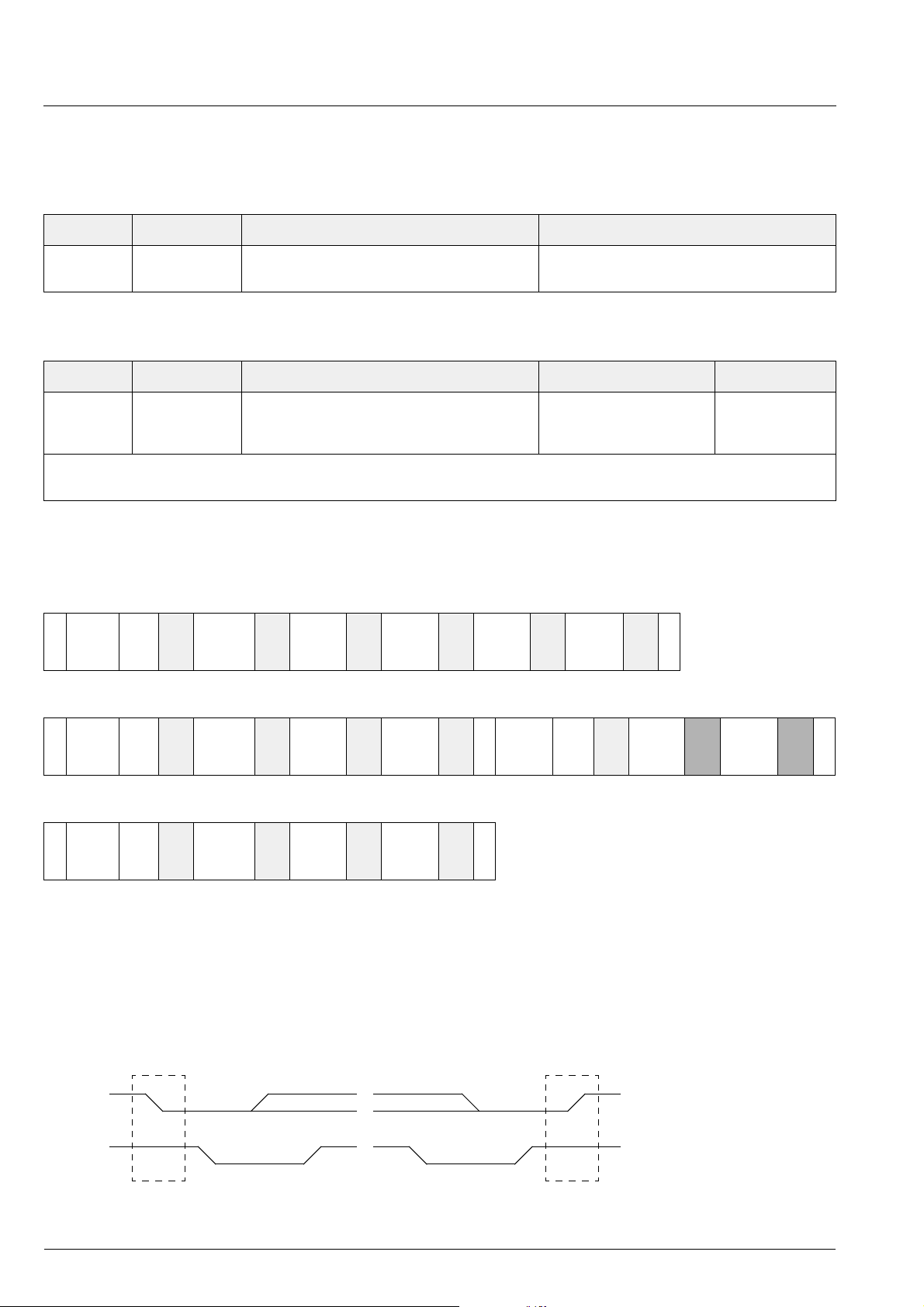
For input signals ranging from −24 dBr to 0 dBr, the
AVC maintains a fixed output level of −18 dBr. Fig. 2–4
shows the AVC output level versus its input level. For
prescale and volume registers set to 0 dB, a level of
0 dBr corresponds to full scale input/output. This is
Any source can be selected as the input for the two
channels of the Mixi ng unit. The mixer channel matr ices and the scal ing factors can be programmed separately for each channel.
After adding up both channels, the signal is fed back
and is available as source 15 (Mix output) of the
Source Selector.
– SCART input/output 0 dBr = 2.0 V
– Main and Aux output 0 dBr = 1.4 V
rms
rms
output level
[dBr]
12
−
18
−
24
−
30−24−18−12
−
6
−
0
Fig. 2–4: Simplified AVC characteristics
6
+
input level
[dBr]
12 Micronas
Page 13

PRELIMINARY DATA SHEET MSP 44x8G
2.5.2. Main and Aux Outputs
The Main and Aux output channels ar e adjustable in
volume. A square wave beeper with adjustable frequency and volume can be added to them.
2.5.3. Quasi-Peak Detector
The Quasi-Peak Readout register can be used to read
out the quasi-pe ak level of any input source. The feature is based on following filter time constants:
– attack time: 1.3 ms
– decay time: 37 ms
2.6. SCART Signal Routing
2.6.1. SCART DSP In and SCART Out Select
The SCART DSP Input Select and SCART Output
Select blocks include full matr ix switching facilities. To
design a TV set with four pairs of SCART-inputs and
two pairs of SCART-outputs, no external switching
hardware is required. The switches are controlled by
the ACB user register (see page 31).
2.7.1. Synchronous I
The synchronous I
2
S-Interface(s)
2
S bus interface consists of the
pins:
– I2S_DA_IN1, I2S_DA_IN2/3 (I2S_DA_IN2 in
PQFP80 package):
2
S serial data input, 16, 18...32 bits per sample.
I
– I2S_DA_OUT:
2
S serial data output, 16, 18...32 bits per sample.
I
– I2S_CL:
2
S serial clock.
I
– I2S_WS:
2
S word strobe signal defines the left and right
I
sample.
If the MSP 44x8G serves as the master on the I
2
interface, the clock and word strobe lines are driven by
the MSP. In this mode, only 16, 32 bits per s amp le can
be selected. In slave mode, these lines are input to the
MSP 44x8G and the MSP clock is synchronized to
384 times the I2S_WS rate (48 kHz). NICAM operation
is not possible in slave mode.
2
S timing diagram is shown in Fig. 4–22 on
An I
page 59.
S
2.6.2. Stand-by Mode
If the MSP 44x8G is switched off by first pulling
STANDB YQ l ow and th en (a fter >1µs delay) switching
off the 5-V, but keeping the 8-V power supply ( ‘Stand-
by’- m ode), the SCART switches maintain their position and function. This allows the copying from
selected SCART-inputs to SCART-outputs in the TV
set’s stand-by mode.
In case of power on or starting from stand-by (see
details on the power-up sequence in Fig. 4–20 on
page 56), al l inter na l regi sters except the ACB register
(page 31) are reset to the default configuration (see
Table 3–5 on page 18) . The reset posi tion of the ACB
register becomes active after the fir st I
2
C transmission
into the Baseband Processing part (subaddress
). By transmitting the ACB register first, the reset
12
hex
state can be redefined.
2
S Bus Interfaces
2.7. I
The MSP 44x8G has two kinds of inte rfaces: synchr onous master/slave input/output interfaces running on
48 kHz and an asynchronous slave interface.
2
2.7.2. Asynchronou s I
The asynchronous I
S-Interface
2
S slave interface allows the
reception of digital stereo signals with arbitrary sample
rates from 5 to 50 kHz. The synchronization is performed by means of an adaptive sample rate converter. No oversampling clock is required.
The following pins are used for the asynchron ous I
2
bus interface:
– I2S_WS3 (serves only as input)
– I2S_CL3 (serves only as input)
– I2S_DA_IN2/3 (I2S_DA_IN3 in PQFP80 package).
2
The interface accepts I
S-input streams with M SB first
and with sample widths of 16,18...32 bits. With left/
right alignment and wordstrobe timing polarity, there
are additional paramet ers available for the adaption to
a variety of formats in the I
2
S-CONFIG register (see
page 24).
S
The interfaces accept a variety o f formats with d if ferent
sample width, bit-orientation, and wordstrobe timing.
2
S options are set by means of the MODUS or
All I
2
S_CONFIG register.
I
Micronas 13
Page 14

MSP 44x8G PRELIMINARY DATA SHEET
2.8. ADR Bus Interface
For the ASTRA Digital Radio System (ADR), the
MSP 4408G, M SP 441 8G, and MSP 4458G performs
preprocessing such as carrier selection and filtering.
Via the 3-line ADR-bus, the resulting signals are transferred to the DRP 3510A coprocessor, where the
source decoding i s performed. To b e prepared for an
upgrade to ADR with an a ddi ti onal D RP board, the following lines of MSP 44x8G should be provided on a
feature connector:
– AUD_CL_OUT
– I2S_DA_IN1, 2, or 3
– I2S_DA_OUT, I2S_WS, I2S_CL
– ADR_CL, ADR_WS, ADR_DA
For more details, please refer to the DRP 3510A data
sheet.
2.9. Digital Control I/O Pins and
Status Change Indication
The static level of the digital input/output pins
D_CTR_I/O_0/1 is switchable between HIGH and
LOW via the I
(see page 31). Thi s enables the controlling of external
hardware switches or other devices via I
2
C-bus by means of the ACB register
2
C-bus.
The digital input/ou tput pins can b e set to high imp edance by means of the MODUS register (see page 23).
In this mode, the pins can be used as input. The current state can be rea d ou t of the S TATUS register (see
page 25).
Optionally, the pin D_CTR_I/O_1 can be used as an
interrupt reque st signal to the co ntrol ler, indicating any
changes in the read register STATUS. This makes polling unnecessary, I
2
C bus interactions are reduced to a
minimum (see “STATUS Register” on page 25 and
“MODUS Register” on page 23).
2.10. Preemphasis
When using the Aux output for feeding an external
modulator, a preemphasis can be applied to the r ight
channel.
The signal is sc aled down by −3 dB. An overmodulation protection is i ncluded in the algo rithm which lim its
the output signal to 0 dBFS. Due to the nature of a preemphasis, its gain at hig h frequencies exceeds 3 dB.
Thus, even with 0 dB input si gnals and p rescal er / volume set to 0 dB, clipping can occur.
There are three modes present: preemphasis off,
50µs, and 75µs. (see Table 3–11on page 29) for the
register settings.
2.11. Clock PLL Oscillator and Crystal Specifications
The MSP 44x8G derives all internal system clocks
from the 18.432 MHz oscillator. In NICAM or in I
2
SSlave mode of the synchronous interface, the clock is
phase-locked to the correspo nding source. Therefore,
it is not possible to use NICAM a nd I
2
S-Slave mode of
the synchronous interface at the same time.
For proper performance, the MSP clock oscillator
requires a 18.432-MHz crystal. Note that for the
phase-locked modes (NICAM, I
tighter tolerance are required. Please note also, that
the asynchronous I
2
S3 slave interface uses a different
2
S-Slave), crystals with
locking mechanism and does not require tighter crystal
tolerances.
Remark on using the crystal:
External cap acitors at each crystal pin to ground are
required. They are necessary for tuning the open-loop
frequency of the internal PLL and for stabilizing the frequency in closed-loop operation. The higher the
capacitors, the lower the resulting clock frequency. The
nominal free running frequency should match
18.432 MHz as closely as possible.
Clock measurements should be done at pin
AUD_CL_OUT. This pin must be acti vated for this purpose (see MODUS register on page 23).
14 Micronas
Page 15
PRELIMINARY DATA SHEET MSP 44x8G
3. Control Interface
2
C Bus Interface
3.1. I
3.1.1. Device and Subaddresses
2
The MSP 44x8G is controlled via the I
C bus slave
interface.
The IC is selected by transmitting one of the
MSP 44x8G device addr esses. In order to allow up to
three MSP ICs to be connected to a single bus, an
address select pin (ADR_SEL) has been implemented.
With ADR_SEL pulled to high, low, or left open, the
MSP 44x8G r espon ds to different device address es. A
device address pair is defined as a write address and a
read address (see Table 3–1).
Writing is d one by sending the device write address,
followed by the subaddress byte, two address bytes,
and two data bytes. Reading i s done by sending the
write device address, followed by the subaddre ss byte
and two address bytes. Without sending a sto p condition, reading of the addressed data is completed by
sending the device read address and reading two
bytes of data. Refer to Section 3.1.2. for the I
protocol and to Section 3.4. “Programming Tips” on
page 34 for proposals of MSP 44x8G I
2
C bus
2
C telegrams.
See Table 3–2 for a list of available subaddresses.
Due to the internal architecture of the MSP 44x8G, the
IC cannot react immediately to an I
2
C request. The
typical respons e time is abou t 0.3 ms. If the MSP cannot accept another complete byte of data until it has
performed some other function (for example, serv icing
an internal i nterrupt), it wil l hold the clock line I2C_CL
low to force the transmitter into a wait state. The posi tions within a transmissio n where thi s may happen are
indicated by “Wait” in Section 3.1.3. The maximum
wait period of t he MSP dur ing nor mal operation mode
is less than 1 ms.
Internal hardware error handling:
In case of any internal hardware error (e.g. interruption
of the pow e r sup ply o f th e MSP ), t he MS P’s wait period
is extended to 1.8 ms. After thi s time period elapses,
the MSP releases data and clock lines.
Indication and solving of the error status:
To indicate the error status, the remaining acknowledge bits of the actual I
Additionally, bit[14] of CONTROL is set to one. The
MSP can then be r eset via the I
2
C-protocol will be left high.
2
C bus by transmitting
the reset condition to CONTROL.
Indication of reset:
Besides the possibility of hardware reset, the MSP can
also be reset by means of the RE SET bit in the CONTROL register by the controller via I
2
C bus.
Any reset, even caused by an unstable reset line etc.,
is indicated in bit[15] of CONTROL.
2
A general timing diagram of the I
C Bus is shown in
Fig. 4–21 on page 57.
2
Table 3–1: I
ADR_SEL Low High Left Open
Mode Write Read Write Read Write Read
MSP device address 80
C Bus Device Addresses
hex
81
hex
84
hex
85
hex
88
hex
89
Table 3–2: I2C Bus Subaddresses
Name Binary Value Hex Value Mode Function
CONTROL 0000 0000 00 Read/Write Write: Software reset of MSP (see Table 3–3)
Read: Hardware error status of MSP
TEST 0000 0001 01 Write only for internal use
WR_DEM 0001 0000 10 Write write address demodulator
hex
RD_DEM 0001 0001 11 Write read address demodulator
WR_DSP 0001 0010 12 Write write address DSP
RD_DSP 0001 0011 13 Write read address DSP
Micronas 15
Page 16
MSP 44x8G PRELIMINARY DATA SHEET
3.1.2. Description of CONTROL Register
Table 3–3: CONTROL as a Write Register
Name Subaddress Bit[15] (MSB) Bits[14:0]
CONTROL 00
hex
1 : RESET
0 : normal
0
Table 3–4: CONTROL as a Read Register
Name Subaddress Bit[15] (MSB) Bit[14] Bits[13:0]
CONTROL 00
hex
Reading of CONTROL will reset the bits[15,14] of CONTROL. After Power-on,
Reset status after last reading of CONTROL:
0 : no reset occured
1 : reset occured
Internal hardware status:
not of interest
0 : no error occured
1 : internal error occured
bit[15] of CONTROL will be set; it must be
read once to be reset.
3.1.3. Protocol Description
Write to DSP or Demodulator
Swrite
device
address
Wait
ACK sub-addr ACK addr-byte
high
ACK addr-byte
low
ACK data-byte-
high
ACK data-byte
low
ACK P
Read from DSP or Demodulator
Swrite
device
address
ACK sub-addr ACK addr-byte
Wait
high
ACK addr-byte
low
ACK S read
device
address
Wait
ACK data-byte-
high
ACK data-byte
Write to Control or Test Registers
Swrite
device
address
Wait
Note: S = I
P = I
ACK sub-addr ACK data-byte
2
C-Bus Start Condition from master
2
C-Bus Stop Condition from master
high
ACK data-byte
low
ACK P
ACK = Acknowledge-Bit: LOW on I2C_DA from slave (= MSP, light gray) or master (= controller, dark gray)
NAK = Not Acknowledge-Bit: HIGH on I2C_DA from master (dark gray) to indicate ‘End of Read’
or from MSP indicating internal error state
2
Wait = I
I2C_DA
C-Clock line is held low, while the MSP is processing the I2C command.
1
0
S P
I2C_CL
NAK P
low
2
Fig. 3–1: I
C bus protocol (MSB first; data must be stable while clock is high)
16 Micronas
Page 17

PRELIMINARY DATA SHEET MSP 44x8G
3.1.4. Proposals for General MSP 44x8G
2
C Telegrams
I
3.1.4.1. Symbols
daw write device address (80
dar read device address (81
hex
hex
, 85
hex
hex
or 88
or 89
hex
hex
)
)
, 84
< Start Condition
> Stop Condition
aa Address Byte
dd Data Byte
3.1.4.2. Write Telegrams
<daw 00 d0 00> write to CONTROL register
<daw 10 aa aa dd dd> write data into demodulator
<daw 12 aa aa dd dd> write data into DSP
3.1.4.3. Read Telegrams
<daw 11 aa aa <dar dd dd> read data from demodulator
<daw 13 aa aa <dar dd dd> read data from DSP
3.1.4.4. Examples
3.2. Start-Up Sequence:
Power-Up and I
2
C Controlling
After POWER ON or RESET (see Fig. 4–20 on
page 56), the IC is in an inactive state. All registers are
in the reset position (seeTable 3–5 and Table 3–6), the
analog outputs a re muted. T he con troll er h as to in itial ize all registers for whic h a non-default setting is necessary.
3.3. MSP 44x8G Programming Interface
3.3.1. User Registers Overview
The MSP 44x 8G is control led by means of user registers. The complete lis t of all user registers is given in
the following tables. The regist ers are parti tioned into
the demodulator s ection (sub addre ss 10
for reading) and the baseband proc essing sec-
11
hex
tions (subaddress 12
for writing, 13
hex
Write and r ead registers are 16-bit wide, whereby the
MSB is denoted bit[15]. Transmissions via I
for writing,
hex
for reading).
hex
2
C bus have
to take place in 16-bit words (two byte transfers, with the
most significant byte transferred first). All write register s,
except the demodulator write registers, are readable.
<80 00 80 00> RESET MSP statically
<80 00 00 00> Clear RESET
<80 10 00 20 00 03> Set demodulator to stand. 03
<80 11 02 00 <81 dd dd> Read STATUS
<80 12 00 08 01 20> Set main channel
source to NICAM and
Matrix to STEREO
hex
More examples of typical application protocols are
listed in Section 3.4. “Programming Tips” on page 34.
Unused parts of the 16-bit write registers must be zero.
Addresses not given in this table must not be written.
An overview of all MSP 44x8G write registers is shown
in Table 3–5; all read registers are given in Table 3–6.
Additional read and write registers, together with a
detailed descr ip tion of the manual mode, can be found
in the “Appendix B: Manual Mode” on page 73.
Micronas 17
Page 18
MSP 44x8G PRELIMINARY DATA SHEET
Table 3–5: List of MSP 44x8G Write Registers
Write Register Address
(hex)
I2C Subaddress = 10
; Registers are
hex
not
Bits Description and Adjustable Range Reset See
Page
readable
STANDARD SELECT 00 20 [15:0] Initial Programming of complete Demodulator 00 00 21
2
MODUS 00 30 [15:0] Demodulator, Automatic and I
I2C Subaddress = 12
; Registers are
hex
all
readable by using I2C Subaddress = 13
hex
S options 00 00 22
Volume main channel 00 00 [15:8] [+12 dB ... −114 dB, MUTE] MUTE 29
[7:5]
[4:0]
1/8 dB Steps
must be set to 0
000
bin
00000
bin
Volume Aux channel 00 06 [15:8] [+12 dB ... −114 dB, MUTE] MUTE 29
[7:5]
[4:0]
1/8 dB Steps
must be set to 0
000
bin
00000
bin
Volume SCART1 output channel 00 07 [15:8] [+12 dB ... −114 dB, MUTE] MUTE 30
2
Main source select 00 08 [15:8] [ FM/AM, NICAM, SCART, I
S1..3, Mix output] FM/AM 28
Main channel matrix [7:0] [SOUNDA, SOUNDB, STEREO, MONO] SOUNDA 28
2
Aux source select 00 09 [15:8] [ FM/A M, NICAM , SC ART, I
S1..3, Mix output] FM/AM 28
Aux channel matrix [7:0] [SOUNDA, SOUNDB, STEREO, MONO] SOUNDA 28
2
SCART1 source select 00 0A [15:8] [FM/AM, NICAM, SCART, I
S1..3, Mix output] FM/AM 28
SCART1 channel matrix [7:0] [SOUNDA, SOUNDB, STEREO, MONO] SOUNDA 28
2
S source select 00 0B [15:8] [FM/AM, NICAM, SCART, I2S1..3, Mix output] FM/AM 28
I
2
S channel matrix [7:0] [SOUNDA, SOUNDB, STEREO, MONO] SOUNDA 28
I
2
Quasi-peak detector source select 00 0C [15:8] [FM/AM, NICAM, SCART, I
S1..3, Mix output] FM /AM 28
Quasi-peak detector matrix [7:0] [SOUNDA, SOUNDB, STEREO, MONO] SOUNDA 28
Prescale SCART input 00 0D [15:8] [00
Prescale FM/AM 00 0E [15:8] [00
hex
hex
... 7F
... 7F
]00
hex
]00
hex
hex
hex
27
26
FM matrix [7:0] [NO_MAT, GSTEREO, KSTEREO] NO_MAT 27
Prescale NICAM 00 10 [15:8] [00
2
Prescale I
Prescale I
S3 00 11 [15:8] [00
2
S2 00 12 [15:8] [00
hex
hex
hex
... 7F
... 7F
... 7F
SCART switches and D_CTR_I/O 00 13 [15:0] Bits [15:0] 00
Beeper 00 14 [15:0] [00
2
Prescale I
S1 00 16 [15:8] [00
hex
hex
... 7F
... 7F
]00
hex
]10
hex
]10
hex
]/[00
hex
hex
... 7F
hex
]10
] 00/00
hex
hex
hex
hex
hex
hex
hex
27
27
27
31
32
27
AVC: Aut omatic Volume Correction 00 29 [15:8] [off, on, decay time] off 29
Aux Preemphasis on right channel 00 34 [15:8] [ OFF, 50µs, 75µs] OFF 29
2
Mix1 source select 00 38 [15:8] [FM/AM, NICAM, SCART, I
S1..3, Mix output] FM/AM 28
Mix1 channel matrix [7:0] [SOUNDA, SOUNDB, STEREO, MONO] SOUNDA 28
2
Mix2 source select 00 39 [15:8] [FM/AM, NICAM, SCART, I
S1..3, Mix output] FM/AM 28
Mix2 channel matrix [7:0] [SOUNDA, SOUNDB, STEREO, MONO] SOUNDA 28
Scale Mix1 00 3A [15:8] [00
Scale Mix2 00 3B [15:8] [00
hex
hex
... 7F
... 7F
]00
hex
]00
hex
hex
hex
32
32
18 Micronas
Page 19
PRELIMINARY DATA SHEET MSP 44x8G
Table 3–5: Lis t of MSP 44x8G Write Register s, co ntinue d
Write Register Address
Bits Descript ion and Adjustable Range Reset See
(hex)
Volume SCAR T2 output channel 00 40 [15:8] [+12 dB ... −114 dB, MUTE] 00
2
SCART2 source select 00 41 [15:8] [FM/AM, NICAM, SCART, I
S1..3, Mix output] FM 28
hex
SCART2 channel matrix [7:0] [SOUNDA, SOUNDB, STEREO, MONO] SOUNDA 28
Table 3–6: List of MSP 44x8G Read Registers
Read Register Address
(hex)
I2C Subaddress = 11
; Registers are
hex
not
STANDARD RESULT 00 7E [15:0] Result of Automatic Standard Detection (see Table 3–8) 25
STATUS 02 00 [15:0] Monitoring of settings e.g. Stereo, Mono, Mute, D_CTR_I/O etc. . 25
I2C Subaddress = 13
; Registers are
hex
not
writable
Quasi peak readout left 00 19 [15:0] [00
Quasi peak readout right 00 1A [15:0] [00
MSP hardware version code 00 1E [15:8] [00
MSP major revision code [7:0] [00
MSP product code 00 1F [15:8] [00
MSP ROM version code [7:0] [00
Bits Descript ion and Adjustable Range See
writable
... 7FFF
hex
... 7FFF
hex
... FF
hex
... FF
hex
... FF
hex
... FF
hex
]16 bit two’s complement 33
hex
]16 bit two’s complement 33
hex
]33
hex
]33
hex
]33
hex
]33
hex
Page
30
Page
Micronas 19
Page 20
MSP 44x8G PRELIMINARY DATA SHEET
3.3.2. Description of User Registers
Table 3–7: Standard Codes for STANDARD SELECT register
MSP Standard
Code
(Data in hex)
TV Sound Standard Sound Carrier
Frequencies in
MHz
MSP 44x8G
Version
Automatic Standard Detection
00 01 Start Automatic Standard Detection all
Standard Selection
00 02 M-Dual FM-Stereo 4.5/4.724212 4408, 4418, 4448,
4458
00 03 B/G-Dual FM-Stereo
00 04 D/K1-Dual FM-Ster eo
00 05 D/K2-Dual FM-Ster eo
1)
2)
2)
00 06 D/K-FM-Mono with HDEV3
Automatic Standard Detection, for China
HDEV3
3)
SAT-Mono (i.e. Eutelsat,
3)
, not detectable by
5.5/5.7421875 4408, 4418, 4458
6.5/6.2578125
6.5/6.7421875
6.5
see Table 6–12)
00 07 D/K3-Dual FM-Stereo 6.5/5.7421875 4408, 4418, 4458
00 08 B/G-NICAM-FM
1)
5.5/5.85 4418, 4458
00 09 L-NICAM-AM 6.5/5.85
00 0A I-NICAM-FM 6.0/6.552
00 0B D/K-NICAM-FM
2)
00 0C D/K-NICAM-FM with HDEV2
4)
, not detectable by
6.5/5.85
6.5/5.85
Automatic Standard Detection, for China
00 0D D/K-NICAM-FM with HDEV3
, not detectable by
6.5/5.85 4418, 4458
3)
Automatic Standard Detection, for China
00 20 BTSC-Stereo 4.5 4438, 4448, 4458
00 21 BTSC-Mono + SAP
00 30 EIA-J Japan Stereo 4.5 4448, 4458
00 40 FM-Stereo Radio 10.7 4438, 4448, 4458
00 50 SAT-Mono (see Table6–12) 6.5 4408, 4418, 4458
00 51 SAT-Stereo (see Table 6–12) 7.02/7.20 4408, 4418, 4458
00 60 SAT ADR (Astra Digital Radio) 6.12 4408, 4418, 4458
1)
In case of Automatic Sound Select, the B/G-codes 3
2)
In case of Automatic Sound Select, the D/K-codes 4
3)
HDEV3: Max. FM deviation must not exceed 540 kHz
4)
HDEV2: Max. FM deviation must not exceed 360 kHz
hex
hex
and 8
, 5
hex
are equivalent.
hex
, 7
and B
hex
are equivalent.
hex
20 Micronas
Page 21
PRELIMINARY DATA SHEET MSP 44x8G
3.3.2.1. STANDARD SELECT Register
The TV sound standard of the MSP 44x8G demodulator is determined by the STANDARD SELECT register.
There are two ways to use the STANDARD SELECT
register:
– Setting up the demodulator for a TV sound standard
by sending the corresponding standard code with a
single I
2
C-Bus transmission.
– Starting the Automatic Standard Detection for ter-
restrial TV s tandards. This is the most comfor table
way to set up the demodulator. Within 0.5 s, the
detection and set-up of the actual TV sound standard is performed. The detected standard can be
read out of the STANDARD RESULT register by the
control process or. This feature is recommende d for
the primary set-up of a TV set. Output s should be
muted during Automatic Standard Detection.
The Standard Codes are listed in Table 3–7.
Selecting a TV sound standard via the STANDARD
SELECT register initializes the demodulator. This
includes: AGC, tuning frequency, band-pass filters,
demodulation mode (FM, AM, or NICAM), carrier
mute, deemphasis, and identification mode.
If a present sound sta nda rd is im pos s ible for a specifi c
MSP version, it switches to the analog m ono soun d of
this standard. In that case, stereo or bi lingual processing will not be possible.
As long as the STANDARD RESULT register contains
a value greater than 07 FF
, the Automatic Standard
hex
Detection is still active. During this period, the MODUS
and STA NDARD SELECT regi ste r must not be written.
The STATUS regist er will be updated when the Automatic Standard Detection has finished.
If a present sound sta nda rd is im pos sible for a spec ifi c
MSP version, it detects and switches to the analog
mono sound of this standard.
Example:
The MSPs 4438G and 4448G will detect a B/G-NICAM
signal as stand ard 3 and will switch to t he analog FMMono sound.
Table 3–8: Results of the Automatic Standard
Detection
Broadcasted Sound
Standard
Automatic Standard
Detection could not
find a sound standard
B/G-FM 0003
B/G-NICAM 0008
I 000A
STANDARD RESULT Register
Read 007E
0000
hex
hex
hex
hex
hex
For a complete setup of the TV sound processing from
analog IF input to the source selection, the following
transmissions are necess ary : MODUS register, STANDARD SELECT register, prescale values, FM matrix.
Note: The FM matrix is set automatically if Automatic
Sound Select is active (MODUS[0]=1). In this case, the
FM matrix will b e i nit ial ized w ith “S ou nd A Mo no”. Du ring operation, the FM matrix will be automatically
selected according to the actual identif ication information.
3.3.2.2. STANDARD RESULT Register
If Automatic Standard Detection is selected in the
STANDARD SELEC T register, status and res ult of the
Automatic Standard Detection process can be read out
of the STANDARD RESULT register. The possible
results are based on the mentioned Standard Code
and are listed in Table 3–8.
In cases where no s ound st andard h as been detected
(no standard present , too much noise, strong interferers, etc.) the STANDARD RESULT register contains
00 00
. In that case, the controller has to start further
hex
actions (for example, set the standard according to a
preference list or by manual input).
FM-Radio 0040
M-FM
EIA-J
BTSC
L-AM
D/K1
D/K2
L-NICAM
D/K-NICAM
Automatic Standard
Detection still activ e
0002
0020
0030
0009
0004
0009
000B
>07FF
hex
(if MODUS[14,13]=00)
hex
(if MODUS[14,13]=01)
hex
(if MODUS[14,13]=10)
hex
(if MODUS[12]=0)
hex
(if MODUS[12]=1)
hex
(if MODUS[12]=0)
hex
(if MODUS[12]=1)
hex
hex
Micronas 21
Page 22

MSP 44x8G PRELIMINARY DATA SHEET
3.3.2.3. Write Registers on I2C Subaddress 10
Table 3–9: Write Registers on I2C Subaddress 10
Register
Function Name
Address
STANDARD SELECTION
00 20
hex
STANDARD SELECTION Register
Defines TV Sound or FM-Radio Standard
bit[15:0] 00 01
00 02
start Automatic Standard Detection
hex
Standard Codes (see Table 3–7))
hex
...
hex
00 60
hex
hex
STANDARD_SEL
22 Micronas
Page 23

PRELIMINARY DATA SHEET MSP 44x8G
Table 3–9: Write Registers on I
Register
Function Name
Address
MODUS
00 30
hex
MODUS Register
General MSP 44x8G Options
bit[15] 0 undefined, must be 0
bit[14:13] detected 4.5 MHz carrier is interpreted as:
0 standard M (Korea)
1 standard M (BTSC)
2 standard M (Japan)
3 Carrier at 4.5 MHz is ignored (chroma carrier)
Preference in Automatic Standard Detection:
bit[12] detected 6.5 MHz carrier is interpreted as:
0 standard L (SECAM)
1 standard D/K1, D/K2, or D/K NICAM
bit[11:9] 0 undefined, must be 0
bit[8] 0/1 ANA_IN_1+/ANA_IN_2+;
2
C Subaddress 10
, continued
hex
select analog sound IF input pin
MODUS
1)
1)
bit[7] 0/1 active/tristate state of audio clock output pin
AUD_CL_OUT
bit[6] word strobe alignment (synchronous I
0 WS changes at data word boundary
1 WS changes one clock cycle in advance
bit[5] 0/1 master/slave mode of I
(= Master) in case of NICAM mode)
bit[4] 0/1 active/tristate state of I
bit[3] state of digital output pins D_CTR_I/O_0 and _1
0 active: D_CTR_I/O_0 and _1 are output pins
(can be set by means of the ACB register.
see also: MODUS[1])
1 tristate: D_CTR_I/O_0 and _1 are input pins
(level can be read out of STATUS[4,3])
bit[2] 0 undefined, must be 0
bit[1] 0/1 disable/enable STATUS change indication by means of
the digital I/O pin D_CTR_I/O_1
Necessary condition: MODUS[3] = 0 (active)
bit[0] 0/1 off/on: Automatic Sound Select
1)
Valid at the next start of Automatic Standard Detection.
2
S)
2
S interface (must be set to 0
2
S output pins
Micronas 23
Page 24

MSP 44x8G PRELIMINARY DATA SHEET
Table 3–9: Write Registers on I
Register
Function Name
Address
0040
hex
I2S Configuration Register
(not mentioned bit combinations must not be used)
bit[15:12] 0 undefined, must be set to 0
bit[11] I
0 left aligned
1 right aligned
bit[10] word strobe polarity (I
1 0 = right, 1 = left
0 1 = right, 0 = left
bit[9] word strobe alignment (asynchronous I
0 WS changes at data word boundary
1 WS changes one clock cycle in advance
bit[8:2] 0 undefined, must be set to 0
bit[1:0] I2S_CL frequency and I
00 2 * 16Bit (1.536MHz Clk)
01 2 * 32Bit (3.072MHz Clk)
1x undefined, must not be used
2
C Subaddress 10
2
S Data alignment (I2S_3)
, continued
hex
2
S_3)
2
S_3)
2
S_DA_OUT sample length
I2S_CONFIG
24 Micronas
Page 25

PRELIMINARY DATA SHEET MSP 44x8G
3.3.2.4. Read Registers on I2C Subaddress 11
hex
Table 3–10: Read Registers on I2C Subaddress 11
Register
Function Name
Address
STANDARD RESULT
00 7E
hex
STANDARD RESULT Register
Readback of the detected TV Sound or FM-Radio Standard
bit[15:0] 00 00
Automatic Standard Detection could not find
hex
a sound standard
00 02
MSP Standard Codes (see Table 3–8)
hex
...
00 40
>07 FF
hex
Automatic Standard Detection still active
hex
STATUS
02 00
hex
STATUS Register
Contains all user relevant internal information about the status of the MSP
hex
STANDARD_RES
STATUS
bit[15:10] undefined
bit[8] 0/1 “1” indicates bilingual sound mode or SAP present
bit[7] 0/1 “1” indicates independent mono sound
(only for NICAM on MSP 4418G and MSP 4458G)
bit[6] 0/1 mono/stereo indication
bit[5,9] 00 analog sound standard (FM or AM) active
01 this pattern will not occur
10 digital sound (NICAM) available (MSP 4418G and
MSP 4458G only)
11 bad receptio n co nd itio n o f di gi ta l so un d (N ICAM ) du e to :
a. high error rate
b. unimplemented sound code
c. data transmission only
bit[4] 0/1 low/high level of digital I/O pin D_CTR_I/O_1
bit[3] 0/1 low/high level of digital I/O pin D_CTR_I/O_0
bit[2] 0 detected secondary carrier (2nd A2 or SAP carrier)
1 no secondary carrier detected
bit[1] 0 detected primary carrier (Mono or MPX carrier)
1 no primary carrier detected
bit[0] undefined
If STATUS change indication is activated by means of MODUS[1]: Each
change in the ST ATUS register sets the digital I/O pin D_CTR_I/O_1 to high
level. Reading the STATUS register resets D_CTR_I/O_1.
Micronas 25
Page 26

MSP 44x8G PRELIMINARY DATA SHEET
3.3.2.5. Write Registers on I2C Subaddress 12
hex
Table 3–11: Write Registers on I2C Subaddress 12
Register
Function Name
Address
PREPROCESSING
00 0E
hex
FM/AM Prescale
bit[15:8] 00
7F
00
hex
hex
hex
... Defines the input prescale gain for the demodulated FM or
AM signal
off (RESET condition)
For all FM modes except satellite FM, the combinations of prescale value and
FM deviation listed below lead to internal full scale.
FM mode
bit[15:8] 7F
48
30
24
18
13
hex
hex
hex
hex
hex
hex
28 kHz FM deviation
50 kHz FM deviation
75 kHz FM deviation
100 kHz FM deviation
150 kHz FM deviation
180 kHz FM deviation (limit)
hex
PRE_FM
FM high deviation mode (HDEV2, MSP Standard Code = C
bit[15:8] 30
14
hex
hex
150 kHz FM deviation
360 kHz FM deviation (limit)
hex
)
FM very high deviation mode (HDEV3, MSP Standard Code = 6)
bit[15:8] 20
1A
hex
hex
450 kHz FM deviation
540 kHz FM deviation (limit)
Satellite FM with adaptive deemphasis
bit[15:8] 10
hex
recommendation
AM mode (MSP Standard Code = 9)
bit[15:8] 7C
hex
recommendation for SIF input levels from
0.1 V
to 0.8 V
pp
pp
(Due to the AGC switched on, the AM-output level remains
stable and independent of the actual SIF-level in the mentioned input range)
26 Micronas
Page 27

PRELIMINARY DATA SHEET MSP 44x8G
Table 3–11: Write Registers on I
Register
Function Name
Address
(continued)
00 0E
hex
FM Matrix Modes
Defines the dematrix function for the demodulated FM signal
bit[7:0] 00
01
02
03
04
hex
hex
hex
hex
hex
In case of Automatic Sound Select, the FM Matrix Mode is set autom atically,
i.e. the low-part of any I
To enable a Forced Mono Mode for all analog stereo systems by overriding the
internal pilot or id en ti fica ti on evalua ti on , t he following ste ps m u st be transmitted:
1. MODUS with bit[0] = 0 (Automatic Sound Select off)
2. FM Presc./Matrix with FM Matrix = Sound A Mono (SAP: Sound B Mono)
3. Select FM/AM source channel, with channel matrix set to “Stereo” (transparent)
2
C Subaddress 12
, continued
hex
no matrix (used f o r bi lin gu al and un ma trixed stereo soun d)
German stereo (Standard B/G)
Korean stereo (also used for BTSC, EIA-J, and FM Radio)
sound A mono (left and right channel contain the mono
sound of the FM/AM mono carrier)
sound B mono (i.e. SAP)
2
C transmission to the register 00 0E
is ignored.
hex
FM_MATRIX
00 10
00 16
00 12
00 11
00 0D
hex
hex
hex
hex
hex
NICAM Prescale
Defines the input prescale value for the digital NICAM signal
bit[15:8] 00
hex
... 7F
prescale gain
hex
examples:
00
20
5A
7F
hex
hex
hex
hex
off
0dB gain
9 dB gain (recommendation)
12 dB gain (maximum gain)
+
I2S1 Prescale
I2S2 Prescale
I2S3 Prescale
2
Defines the input prescale value for digital I
bit[15:8] 00
hex
... 7F
prescale gain
hex
S input signals
examples:
00
10
7F
hex
hex
hex
off
0 dB gain (recommendation)
18 dB gain (maximum gain)
+
SCART Input Prescale
PRE_NICAM
PRE_I2S1
PRE_I2S2
PRE_I2S3
PRE_SCART
Defines the input prescale value for the analog SCART input signal
bit[15:8] 00
hex
... 7F
prescale gain
hex
examples:
00
19
7F
hex
hex
hex
off
0dB gain (2 V
14 dB gain (400 mV
+
RMS
input leads to digital full scale)
input leads to digital full scale)
RMS
Micronas 27
Page 28

MSP 44x8G PRELIMINARY DATA SHEET
Table 3–11: Write Registers on I
Register
Function Name
2
C Subaddress 12
hex
Address
SOURCE SELECT AND OUTPUT CHANNEL MATRIX
Source for:
00 08
00 09
00 0A
00 41
00 0B
00 0C
00 38
00 39
hex
hex
hex
hex
hex
hex
hex
hex
Main Output
Aux Output
SCART1 DA Output
SCART2 DA Output
2
S Output
I
Quasi-Peak Detector
Mix1 Input
Mix2 Input
bit[15:8] 0 “FM/AM”: demodulated FM or AM mono signal
1 “Stereo or A/B”: demodulator Stereo or A/B signal
3 “Stereo or A”: demodulator Stereo Sound or
Language A (only defined for Automatic Sound Select)
4 “Stereo or B”: demodulator Stereo Sound or
Language B (only defined for Automatic Sound Select)
, continued
SRC_MAIN
SRC_AUX
SRC_SCART1
SRC_SCART2
SRC_I2S
SRC_QPEAK
SRC_MIX1
SRC_MIX2
00 08
00 09
00 0A
00 41
00 0B
00 0C
00 38
00 39
hex
hex
hex
hex
hex
hex
hex
hex
2 SCART input
2
5I
6I
7I
S1 input
2
S2 input
2
S3 input
15 Mix output
For demodulator sources, see Table 2–2.
Matrix Mode for:
Main Output
Aux Output
SCART1 DA Output
SCART2 DA Output
2
S Output
I
Quasi-Peak Detector
Mix1 Input
Mix2 Input
bit[7:0] 00
10
20
30
hex
hex
hex
hex
Sound A Mono (or Left Mono)
Sound B Mono (or Right Mono)
Stereo (transparent mode)
Mono (sum of left and right inputs divided by 2)
More modes are listed in Section 6.5.1.
MAT_MAIN
MAT_AUX
MAT_SCART1
MAT_SCART2
MAT_I2S
MAT_QPEAK
MAT_MIX1
MAT_MIX2
In Automatic Sound Select mode, the demodulator source channels are set
according to T ab le 2–2. Therefore, the matrix modes of the corresponding output
channels should be set to “Stereo” (transparent).
28 Micronas
Page 29

PRELIMINARY DATA SHEET MSP 44x8G
Table 3–11: Write Registers on I
Register
Function Name
Address
MAIN AND AUX PROCESSING
00 00
00 06
hex
hex
Volume Main
Volume Aux
bit[15:8] volume table with 1 dB step size
7F
hex
7E
hex
...
74
hex
73
hex
72
hex
...
02
hex
01
hex
00
hex
FF
hex
bit[7:5] higher resolution volume table
0
1
...
7
2
C Subaddress 12
12 dB (maximum volume)
+
11 dB
+
1dB
+
, continued
hex
0dB
1dB
−
113 dB
−
114 dB
−
Mute (reset condition)
Fast Mute (needs about 75 ms until the signal is completely ramped down)
0dB
+
0.125 dB increase in addition to the volume table
+
0.875 dB increase in addition to the volume table
+
VOL_MAIN
VOL_AUX
0029
00 34
hex
hex
bit[4:0] not used
must be set to 0
With large scale input signals , positive volume settings may lead to signal clipping.
The MSP 44x8G Main and Aux volume function is divided into a dig ital and an
analog section. With Fast Mute, volume is reduced to mute position by digital volume only. Analog volume is not changed. This reduces any audible DC plops. To
turn volume on again, the volume step that has been used before Fast Mute was
activated must be transmitted.
Automatic Volume Correction (AVC)
bit[15] 0 AVC off, reset of internal variables
1AVC on
bit[14] 0 AVC in Main path
1 AVC in Mixer path
bit[13:12] 0 must be set to zero
bit[11:8] 8 8 s decay time
4 4 s decay time (recommended)
2 2 s decay time
1 20 ms decay time (should be used for approx. 100 ms
after channel change)
Preemphasis Aux Channel
AVC
AVC_DECAY
PREEMP_AUX
bit[15:8] 00
7F
FF
hex
hex
hex
Preemphasis OFF
Preemphasis 50µs (−3 dB scaling)
Preemphasis 75µs (−3 dB scaling)
Micronas 29
Page 30

MSP 44x8G PRELIMINARY DATA SHEET
Table 3–11: Write Registers on I
Register
Function Name
Address
SCART OUTPUT CHANNEL
00 07
00 40
hex
hex
Volume SCART1 Output Channel
Volume SCART2 Output Channel
bit[15:8] v olume table with 1 dB step size
7F
hex
7E
hex
...
74
hex
73
hex
72
hex
...
02
hex
01
hex
00
hex
bit[7:5] higher resolution volume table
0
1
...
7
2
C Subaddress 12
12 dB (maximum volume)
+
11 dB
+
1dB
+
, continued
hex
0dB
1dB
−
113 dB
−
114 dB
−
Mute (reset condition)
0 dB
+
0.125 dB increase in addition to the volume table
+
0.875 dB increase in addition to the volume table
+
VOL_SCART1
VOL_SCART2
bit[4:0] 01
hex
this must be 01
hex
30 Micronas
Page 31

PRELIMINARY DATA SHEET MSP 44x8G
Table 3–11: Write Registers on I
Register
Function Name
2
C Subaddress 12
Address
SCART SWITCHES AND DIGITAL I/O PINS
00 13
hex
ACB Register
Defines the level of the digital output pins and the position of the SCART switches
bit[15] 0/1 low/high of digital output pin D_CTR_I/O_0
(MODUS[3]=0)
bit[14] 0/1 low/high of digital output pin D_CTR_I/O_1
(MODUS[3]=0)
bit[13:5] SCART DSP Input Select
xxxx00 xx0 SCART1 to DSP input (RESET position)
xxxx01 xx0 MONO to DSP input (Sound A Mono must be selected in
the channel matrix mode for the corresponding output
channels)
xxxx10 xx0 SCART2 to DSP input
xxxx11 xx0 SCART3 to DSP input
xxxx00 xx1 SCART4 to DSP input
xxxx11 xx1 mute DSP input
, continued
hex
ACB_REG
bit[13:5] SCART1 Output Select
xx00xx x0x SCART3 input to SCART1 output (RESET position)
xx01xx x0x SCART2 input to SCART1 output
xx10xx x0x MONO input to SCART1 output
xx11xx x0x SCART1 DA to SCART1 output
xx00xx x1x SCART2 DA to SCART1 output
xx01xx x1x SCART1 input to SCART1 output
xx10xx x1x SCART4 input to SCART1 output
xx11xx x1x mute SCART1 output
bit[13:5] SCART2 Output Select
00xxxx 0xx SCAR T1 DA to SCART2 output (RESET position)
01xxxx 0xx SCART1 input to SCART2 output
10xxxx 0xx MONO input to SCART2 output
00xxxx 1xx SCART2 DA to SCAR T2 output
01xxxx 1xx SCART2 input to SCART2 output
10xxxx 1xx SCART3 input to SCART2 output
11xxxx 1xx SCART4 input to SCART2 output
11xxxx 0xx mute SCART2 output
The RESET position becomes active at the time of the first write transmission on
the control bus to the audio pr ocessing p ar t. By wri ting to the ACB regis ter first,
the RESET state can be redefined.
Micronas 31
Page 32

MSP 44x8G PRELIMINARY DATA SHEET
Table 3–11: Write Registers on I
Register
Function Name
Address
MIXING UNIT
00 3A
00 3B
hex
hex
MIX1 Scale
MIX2 Scale
Defines the input scale value for the digital mixing unit
bit[15:8] 00
20
40
7F
hex
hex
hex
hex
Note: If the sum of both mixing inputs exceeds 100%, clipping may occur in the
successive processing.
BEEPER
00 14
hex
Beeper Volume and Frequency
bit[15:8] Beeper Vo lu me
00
hex
7F
hex
bit[7:0] Beeper Frequency
01
hex
40
hex
FF
hex
2
C Subaddress 12
, continued
hex
off
50% (−6dB gain)
100% (0 dB gain)
200% (+6 dB gain = maximum gain)
off
maximum volume
16 Hz (lowest)
1kHz
4kHz
VOL_MIX1
VOL_MIX2
BEEPER
32 Micronas
Page 33

PRELIMINARY DATA SHEET MSP 44x8G
3.3.2.6. Read Registers on I2C Subaddress 13
hex
Table 3–12: Read Registers on I2C Subaddress 13
Register
Function Name
Address
QUASI-PEAK DETECTOR READOUT
00 19
00 1A
hex
hex
Quasi-Peak Detector Readout Left
Quasi-Peak Detector Readout Right
bit[15:0] 0
... values are 16 bit two’s complement (only positive)
hex
7FFF
hex
MSP 44x8G VERSION READOUT Registers
001E
hex
MSP Hardware Version Code
bit[15:8] 01
hex
MSP 44x8G-A1
A change in the hardware version code defines hardware optimizations that
may have influence on the chip’s behavior. The readout of this register is identical to the hardware version code in the chip’s imprint.
MSP Family Code
hex
QPEAK_L
QPEAK_R
MSP_HARD
MSP_FAMILY
001F
hex
bit[7:4] 1
hex
MSP 44x8G-A1
MSP Major Revision Code
bit[3:0] 7
hex
MSP 44x8G-A1
MSP Product Code
bit[15:8] 08
12
1C
30
3A
hex
hex
hex
hex
hex
MSP 4408G-A1
MSP 4418G-A1
MSP 4428G-A1
MSP 4448G-A1
MSP 4458G-A1
By means of the MSP-Product Code, the control processor is able to decide
which TV sound standards have to be considered.
MSP ROM Version Code
bit[7:0] 41
hex
MSP 44x8G-A1
A change in the ROM version code defines internal software optimizations, that
may have influence on the chip’s behavior, e.g. new features may have been
included. While a software change is intended to create no compatibility problems, customers that want to use the new functions can identify new
MSP 44x8G versions according to this number.
MSP_REVISION
MSP_PRODUCT
MSP_ROM
Micronas 33
Page 34

MSP 44x8G PRELIMINARY DATA SHEET
3.4. Programming Tips
This section desc ribes the pr eferred method for initializing the MSP 44x8G. The initialization is grou ped int o
four sections:
– SCART Signal Path (analog signal path)
– Demodulator Input
2
– SCART and I
S Inputs
– Output Channels
See Fig. 2–1 on page 8 for a complete signal flow.
SCART Signal Path
1. Select analog input for the SCART baseband processing (SCART DSP Input Select) b y me ans of the
ACB register.
2. Select the source for each analog SCART output
(SCART Output Select) by means of the ACB register.
Demodulator Input
For a complete setup of the sound processing from
analog IF input to the source selection, the following
steps must be performed:
1. Set MODUS register to the preferred mode and
Sound IF input.
3.5. Examples of Minimum Initialization Codes
Initialization of the MSP 44x8G according to these listings reproduces sound of the selected standard on the
main output. All num bers are hexadecima l. The examples have the following structure:
1. Perform an I
2
C controlled reset of the IC.
2. Write MODUS register
(with Automatic Sound Select).
3. Set Source Selection for main channel
(with matrix set to STEREO).
4. Set Prescale
(FM and/or NICAM and dummy FM matrix).
5. Wri te STANDARD SELECT register.
6. Set Volume main channel to 0 dB.
3.5.1. B/G-FM (A2 or NICAM)
<80008000>
<80000000>
<801000302003>
<801200080320>
<8012000E2403>
<80120010005A>
<801000200003>
<801000200008>
<801200007300>
or
// Softreset
// MODUS-Regist er: Automatic = on
// So u rce Sel. = (St or A) & Ch . M atr. = St
// FM/AM-Prescale = 24
FM-Matrix = MONO/SOUNDA
// NICAM-Prescale = 5A
// Standard Select: A2 B/G or NICAM B/G
// Main Volume 0 dB
hex
hex
,
2. Write STANDARD SELECT register.
3. Choose preferred prescale (FM and NICAM) values.
4. If Automatic Sound Select is not active:
Choose FM matrix repeatedly according to the
sound mode indicated in the STATUS register.
2
SCART and I
S Inputs
1. Select preferred pre scale for SCART.
2
2. Select preferred prescale for I
S inputs
(set to 0 dB after RESET).
Output Channels
1. Select the source channel and matrix for each output channel.
2. Set audio baseband features (i.e. AVC, 75µs preemphasis)
3. Select volume for each output channel.
3.5.2. BTSC-Stereo
<80008000>
<80000000>
<801000302003>
<801200080320>
<8012000E2403>
<801000200020>
<801200007300>
// Softreset
// MODUS-Regist er: Automatic = on
// So u rce Sel. = (St or A) & Ch . M atr. = St
// FM/AM-Prescale = 24
FM-Matrix = Sound A Mono
// Standard Select: BT SC -ST ERE O
// Main Volume 0 dB
hex
,
3.5.3. BTSC-SAP with SAP at Main Channel
<80008000>
<80000000>
<801000302003>
<801200080420>
<8012000E2403>
<801000200021>
<801200007300>
// Softreset
// MODUS-Regist er: Automatic = on
// So u rce Sel. = (St or B) & Ch . M atr. = St
// FM/AM-Prescale = 24
FM-Matrix = Sound A Mono
// Standard Select : BTSC-SAP
// Main Volume 0 dB
hex
,
34 Micronas
Page 35

PRELIMINARY DATA SHEET MSP 44x8G
3.5.4. FM-Stereo Radio
<80008000>
<80000000>
<801000302003>
<801200080320>
<8012000E2403>
<801000200040>
<801200007300>
// Softreset
// MODUS-Register: Automatic = on
// Source Sel. = (St or A) & Ch. Matr. = St
// FM/AM-Prescale = 24
FM-Matrix = Sound A Mono
// Standard Select: FM-S TE REO -R ADI O
// Main Volume 0 dB
hex
,
3.5.5. Automatic Standard Detection
A detailed software flow diagram is shown in Fig. 3 –2
on page 36.
<80008000>
<80000000>
<801000302003>
<801200080320>
<8012000E2403>
<80120010005A>
<801000200001>
// Wait till STANDARD RESULT contains a value ≤ 07FF
// IF STANDARD RESULT contains 0000
// ELSE
<801200007300>
// Softreset
// MODUS-Register: Automatic = on
// Source Sel. = (St or A) & Ch. Matr. = St
// FM/AM-Prescale = 24
FM-Matrix = Sound A Mono
// NICAM-Prescale =
// Standard Select:
Automatic Standard Detection
// do some error handling
// Main Volume 0 dB
5A
hex
hex
,
3.5.6. Software Flow for
Interrupt driven STATUS Check
A detailed software flow diagram is shown in Fig. 3 –2
on page 36.
If the D_CTR_I/O_1 pin of the MSP 44x8G is connected to an interrupt input pin of the controller, the following interrupt handler can be applied to be automatically called with each status change of the
MSP 44x8G. T he interr upt handl er may adjust the di splay according to the new status information.
Interrupt Handler:
<80 11 02 00 <81 dd dd>
// adjust display with given status information
// R e turn from In terrupt
// Read STATUS
Micronas 35
Page 36

MSP 44x8G PRELIMINARY DATA SHEET
Write MODUS Register
Example
[0] = 1 Automatic Sound Select = on
[1] = 1 Enable interrupt if STATUS changes
[8] = 0 ANA_IN1+ is selected
Define Preference for Automatic Standard
Detection:
[12] = 0 If 6.5 MHz, set SECAM-L
[14:13] = 3 Ignore 4.5 MHz carrier
for the essential bits:
:
Write SOURCE SELECT Settings
Example:
set main Source Select to "Stereo or A"
set aux Source Select to "Stereo or B"
set SCART_Out Source Select to "Stereo or A/B"
set Channel Matrix mode for all outputs to "Stereo"
Write FM/AM-Prescale
Write NICAM-Prescale
set previous standard or
set standard manually according
picture information
In case of interrupt from
MSP to Controller:
Write 01 into
STANDARD SELECT Register
(Start Automatic Standard Detection)
yes
expecting interrupt from MSP
Result = 0
?
no
Read STATUS
Adjust Display
If bilingual, adjust Source Select setting if required
Fig. 3–2: Software flow diagram for a minimum demodulator setup for a European multistandard set applying the
Automatic Sound Select feature
36 Micronas
Page 37

PRELIMINARY DATA SHEET MSP 44x8G
4. Specifications
4.1. Outline Dimensions
65
8
0.15±
0.15±
17.2
1.8
10.3
9.8
80
16
23.2
Fig. 4–1:
80-Pin Plastic Quad Flat Pack
(PQFP80)
Weight approximately 1.61 g
Dimensions in mm
3348
49
0.2±
12
64
1.75
116
1.75
0.2±
12
32
17
4164
241
0.145
1.5
0.04±
0.17
40
0.05±
0.37
25
0.05±
1.3
±0.2
3
0.055±
0.1±
0.05±
0.22
0.05±
1.4
0.1
0.1±
10
0.1±
2.7
0.1
15 x 0.5 = 7.5
0.5
10
0.1±
14
0.1±
0.5
0.1±
0.8
1.8
23 x 0.8 = 18.4
0.1±
15 x 0.5 = 7.5
0.1±
0.1±
8
5
0.1±
20
SPGS705000-1(P80)/1E
0.8
15 x 0.8 = 12.0
D0025/3E
Fig. 4–2:
64-Pin Plastic Low-Profile Quad Flat Pack
(PLQFP64)
Weight approximately 0.35 g
Dimensions in mm
Micronas 37
Page 38

MSP 44x8G PRELIMINARY DATA SHEET
132
3364
57.7
±0.1
0.8
±0.2
3.8
±0.1
3.2
±0.2
1.778
1
±0.05
31 x 1.778 = 55.1
±0.1
0.48
±0.06
20.3
±0.5
0.28
±0.06
18
±0.05
19.3
±0.1
SPGS0016-5(P64)/1E
Fig. 4–3:
64-Pin Plastic Shrink Dual-Inline Package
(PSDIP64)
Weight approximately 9.0 g
Dimensions in mm
38 Micronas
Page 39

PRELIMINARY DATA SHEET MSP 44x8G
4.2. Pin Connections and Short Descriptions
NC = not connected (leave vacant for future compatibility reasons)
TP = Test Pin (leave vacant - pin is used for production test only)
LV = leave vacant
X = obligatory; connect as described in application circuit diagram
PQFP
80-pin
Pin No. Pin Name Type Connection
PLQFP
64-pin
PSDIP
64-pin
(if not used)
Short Description
1 64 8 NC LV Not connected
2
219I2C_CL IN/OUTX I
3 2 10 I2C_DA IN/OUT X I
4 3 11 I2S_CL IN/OUT LV I
5 4 12 I2S_WS IN/OUT LV I
6 5 13 I2S_DA_OUT OUT LV I
7 6 14 I2S_DA_IN1 IN LV I
C clock
2
C data
2
S clock
2
S word strobe
2
S data output
2
S1 data input
8 7 15 ADR_DA OUT LV ADR data output
9 8 16 ADR_WS OUT LV ADR word strobe
10 9 17 ADR_CL OUT LV ADR clock
11
12
−−
−−
DVSUP X Digital power supply +5 V
DVSUP X Digital power supply +5 V
13 10 18 DVSUP X Digital power supply +5 V
14
15
−−
−−
DVSS X Digital ground
DVSS X Digital ground
16 11 19 DVSS X Digital ground
2
−
17
12 20 I2S_DA_IN2/3 IN LV I
−−
I2S_DA_IN2 IN LV
S2/3-data input
PQFP80: pin 22 separate I2S_DA_IN3
18 13 21 NC LV Not connected
2
19 14 22 I2S_CL3 IN LV I
20 15 23 I2S_WS3 IN LV I
S3 clock
2
S3 word strobe
21 16 24 RESETQ IN X P ower-on-reset
2
22
23
−−
−−
I2S_DA_IN3 IN LV I
NC LV Not connected
S3-data input
24 17 25 DACA_R OUT LV Aux out, right
25 18 26 DACA_L OUT LV Aux out, left
26 19 27 VREF2 X Reference ground 2
Micronas 39
Page 40

MSP 44x8G PRELIMINARY DATA SHEET
Pin No. Pin Name Type Connection
PQFP
80-pin
27 20 28 DACM_R OUT LV Main out, right
28 21 29 DACM_L OUT LV Main out, left
29 22 30 NC LV Not connected
30 23 31 NC LV Not connected
31 24 32 NC LV Not connected
32
33 25 33 SC2_OUT_R OUT LV SCART output 2, right
34 26 34 SC2_OUT_L OUT LV SCART output 2, left
35 27 35 VREF1 X Reference ground 1
36 28 36 SC1_OUT_R OUT LV SCART output 1, right
37 29 37 SC1_OUT_L OUT LV SCART output 1, left
38 30 38 CAPL_A X Volume capacitor Aux
PLQFP
64-pin
−−
PSDIP
64-pin
NC LV Not connected
(if not used)
Short Description
39 31 39 AHVSUP X Analog power supply 8.0 V
40 32 40 CAPL_M X Volume capacitor Main
41
42
43
44 33 41 AHVSS X Analog ground
45 34 42 AGNDC X Analog reference voltage
46
47 35 43 SC4_IN_L IN LV SCART 4 input, left
48 36 44 SC4_IN_R IN LV SCART 4 input, right
49 37 45 ASG AHVSS Analog Shield Ground
50 38 46 SC3_IN_L IN LV SCART 3 input, left
51 39 47 SC3_IN_R IN LV SCART 3 input, right
52 40 48 ASG AHVSS Analog Shield Ground
−−
−−
−−
−−
NC LV Not connected
NC LV Not connected
AHVSS X Analog ground
NC LV Not connected
53 41 49 SC2_IN_L IN LV SCART 2 input, left
54 42 50 SC2_IN_R IN LV SCART 2 input, right
55 43 51 ASG AHVSS Analog Shield Ground
56 44 52 SC1_IN_L IN LV SCART 1 input, left
57 45 53 SC1_IN_R IN LV SCART 1 input, right
40 Micronas
Page 41

PRELIMINARY DATA SHEET MSP 44x8G
PQFP
80-pin
Pin No. Pin Name Type Connection
PLQFP
64-pin
PSDIP
64-pin
(if not used)
Short Description
58 46 54 VREFTOP X Reference voltage IF A/D converter
59
−−
NC LV Not connected
60 47 55 MONO_IN IN LV Mono input
61
−−
AVSS X Analog ground
62 48 56 AVSS X Analog ground
63
64
65
−−
−−
−−
NC LV Not connected
NC LV Not connected
AVSUP X Analog power supply +5V
66 49 57 AVSUP X Analog power supply +5V
67 50 58 ANA_IN1
68 51 59 ANA_IN
69 52 60 ANA_IN2
+
−
+
IN LV IF input 1
IN AVSS via
56 pF / LV
IN AVSS via
56 pF / LV
IF common
IF input 1 is also not in use)
IF input 2 (Can be left vacant, only if
IF input 1 is also not in use)
(Can be left vacant, only if
70 53 61 TESTEN IN AVSS Test pin
71 54 62 XTAL_IN IN X Crystal oscillator
72 55 63 XTAL_OUT OUT X / LV Crystal oscillator
“Pin Descriptions” on page42)
(See also Section 4.3.
73 56 64 TP LV Test pin
74 57 1 AUD_CL_OUT OUT LV Audio clock output (18.432 MHz)
75 58 2 NC LV Not connected
76 59 3 NC LV Not connected
77 60 4 D_CTR_I/O_1 IN/OUT LV D_CTR_I/O_1
78 61 5 D_CTR_I/O_0 IN/OUT LV D_CTR_I/O_0
2
79 62 6 ADR_SEL IN X I
C Bus address select
80 63 7 ST ANDBYQ IN X Stand-by (low-active)
Micronas 41
Page 42

MSP 44x8G PRELIMINARY DATA SHEET
4.3. Pin Descriptions
Pin numbers refer to the 80-pin PQFP package.
Pin 1, NC – Pin not connected.
2
Pin 2, I2C_CL – I
Via this pin, the I
C Clock Input/Output (Fig. 4–8)
2
C-bus clock signal has to be supplied. The signal can be pulled down by the MSP in
case of wait conditions.
2
Pin 3, I2C_DA – I
Via this pin, the I
C Data Input/Output (Fig. 4–8)
2
C-bus data is written to or read from
the MSP.
2
Pin 4, I2S_CL – I
Clock line for the synchronous I
mode, this line is driven by the MSP; in slave mode, an
external I
2
S clock has to be supplied.
Pin 5, I2S_WS – I
(Fig. 4–11)
Word strobe line for the synchronous I
ter mode, this line is driven by the MSP; in slave mode,
an external I
Pin 6, I2S_DA_OUT1 – I
Output of digital serial sound data of the MSP on the
synchronous I
Pin 7, I2S_DA_IN1 – I
First input of digital seri al sound data to the MSP via
the synchronous I
S Clock Input/Output (Fig. 4–11)
2
S Word Strobe Input/Output
2
S word strobe has to be supplied.
2
S Data Output (Fig. 4–7)
2
S bus.
2
S Data Input 1 (Fig. 4–9)
2
S bus.
2
S bus. In master
2
S bus. In mas-
Pin 8, ADR_DA – ADR Bus Data Output (Fig. 4–7)
Output of digital ser ial data to the DRP 3510A via the
ADR bus.
Pin 9, ADR_WS – ADR Bus Word Strobe Output
(Fig. 4–7)
Word strobe output for the ADR bus.
Pin 10, ADR_CL – ADR Bus Clock Output (Fig. 4–7)
Clock line for the ADR bus.
Pins 11, 12, 13, DVSUP* – Digital Supply Voltage
Power supply for the digital circuitr y of the MSP. Must
be connected to a +5 V power supply.
Pins 19, I2S_CL3 – I
Clock line for the asynch ronous I
slave mo de is available a n external I
2
S Clock Input (Fig. 4–9)
2
S bus. Since only a
2
S clock has to be
supplied.
2
Pins 20, I2S_WS3 – I
Word strobe line for the asynchronous I
only a slave mode is available an external I
S Word Strobe Input (Fig. 4–9)
2
S bus. Since
2
S word
strobe has to be supplied.
Pin 21, RESETQ – Reset Input (Fig. 4–9)
In the steady state, high level is required. A low level
resets the MSP 44x8G.
2
Pin 22, I2S_DA_IN3 – I
Input of digital serial sound data to the MSP via the
asynchronous I
2
PQFP80, this pin is also connected to synchronous I
S Data Input 3 (Fig. 4–9)
S bus. In all packages except
2
interface 2.
Pins 23, NC – Pin not connected.
Pins 24, 25, DA CA_R/L – Aux Outputs (Fig. 4–17)
Output of the Aux signal. A 1 nF capacitor to AHVSS
must be connected to these pins. The DC offset on
these pins depends on the selected Aux volume.
Pin 26, VREF2 – Reference Ground 2
Reference analog ground. This pi n mus t be co nne cte d
separately to the ground (AHVSS). VREF2 serves as a
clean ground and sho uld be used as the reference for
analog connections to the Main and Aux outputs.
Pins 27, 28, DACM_R/L – Main Outputs
(Fig. 4–17)
Output of the Main signal. A 1 nF capacitor to AHVSS
must be connected to these pins. The DC offset on
these pins depends on the selected Main volume.
Pin 29, 30, 31, 32 NC – Pin not connected.
Pins 33, 34, SC2_OUT_R/L – SCART2 Outputs
(Fig. 4–19)
Output of the SCART2 signal. Connections to these
pins must use a 100-Ω series resist or an d ar e in ten ded
to be AC-coupled.
S
Pins 14, 15, 16, DVSS* – Digital Ground
Ground connection for the digital circuitry of the MSP.
2
Pin 17, I2S_DA_IN2 – I
Second input of digita l serial sound data to the MSP
via the synchronous I
PQFP80, this pin is also connected to the asynchro-
2
nous I
S interface 3.
S Data Input 2 (Fig. 4–9)
2
S bus. In all packages except
Pin 35, VREF1 – Reference Ground 1
Reference analog ground. This pi n mus t be co nne cte d
separately to the ground (AHVSS). VREF1 serves as a
clean ground and sho uld be used as the reference for
analog connections to the SCART outputs.
Pins 36, 37, SC1_OUT_R/L – SCART1 Outputs
(Fig. 4–19)
Output of the SCART1 signal. Connections to these
Pins 18, NC – Pin not connected.
pins must use a 100-Ω series resist or an d ar e in ten ded
to be AC-coupled.
42 Micronas
Page 43

PRELIMINARY DATA SHEET MSP 44x8G
Pin 38, CAPLA – Volume Capacitor Aux (Fig. 4–14)
A 10-µF capacitor to AHVSUP must be connected to
this pin. It se rves as a smoothing f ilter for Aux volume
changes in order to su ppress audible plops. The value
of the capacitor can be lowered to 1-µF if faster
response is requi red. The area encircled by the trace
lines should be minimized; keep traces as short as
possible. This input is sensitive for magnetic induction.
Pin 39, AHVSUP* – Ana log Power Supply High Voltage
Power is supplied via this pin for the analog c irc ui try of
the MSP (except IF input). This pin must be connected
to the +8 V supply. (+5 V-operation is possible with
restrictions in performance)
Pin 40, CAPLM – Volume Capacitor Main (Fig. 4–14)
A 10-µF capacitor to AHVSUP must be connected to
this pin. It serves as a smoothing filter for Main volume
changes in order to su ppress audible plops. The value
of the capacitor can be lowered to 1µF if faster
response is requi red. The area encircled by the trace
lines should be minimized; keep traces as short as
possible. This input is sensitive for magnetic induction.
Pins 41, 42, NC – Pins not connected.
Pins 43, 44, AHVSS* – Analog Power Supply High
Voltag e
Ground connection for the analog circuitr y o f the MS P
(except IF input).
Pin 45, AGNDC – Internal Analog Reference Voltage
This pin ser ves as the internal ground c onnection for
the analog circuitr y (except IF input). It must be connected to the VREF pins with a 3.3-µF and a 100-nF
capacitor in parallel. This pins shows a DC level of typically 3.73 V.
Pins 56, 57 SC1_IN_L/R – SCART1 Inputs (Fig. 4–16)
The analog input sig nal for SCART1 is fed to this pin.
Analog input connection must be AC-coupled.
Pin 58, VREFTOP – Reference Voltage IF A/D Converter (Fig. 4–13)
Via this pin, the reference voltage for the IF A/D converter is decoupled. It must be connected to AVSS
pins with a 10-µF and a 100-nF capac itor in parallel.
Traces must be kept short.
Pin 59, NC – Pin not connected.
Pin 60 MONO_IN – Mono Input (Fig. 4–16)
The analog mono input signal is fed to this pin . A nal og
input connection must be AC-coupled.
Pins 61, 62, AVSS* – Analog Power Supply Voltage
Ground connect ion for the analog IF input circuitry of
the MSP.
Pins 63, 64, NC – Pins not connected.
Pins 65, 66, AVSUP* – Analog Power Supply Voltage
Power is supplied via this pin for the analog IF input circuitry of the MSP. This pin must be connected to the
5V supply.
+
Pin 67, ANA_IN1+ – IF Input 1 (Fig. 4–13)
The analog sound IF signal is supplied to this pin.
Inputs must be AC-coupled. This pin is designed as
symmetrical input: ANA_IN1+ is internally connected
to one input of a symmetr ical op amp, ANA_IN- to the
other.
Pin 68, ANA_IN− – IF Common (Fig. 4–13)
This pins serves as a common reference for ANA_IN1/
2+ inputs and must be AC-coupled.
Pin 46, NC – Pin not connected.
Pins 47, 48, SC4_IN_L/R – SCART4 Inputs
(Fig. 4–16)
The analog input s ignal for SCART4 is fed to this pin.
Analog input connection must be AC-coupled.
Pins 49, 52, and 55, ASG* – Analog Shield Gr ound
Analog ground (AHVSS) should be connected to this
pin to reduce cross-coupling between SCART inputs.
Pins 50, 51, SC3_IN_L/R – SCART3 Inputs
(Fig. 4–16)
The analog input s ignal for SCART3 is fed to this pin.
Analog input connection must be AC-coupled.
Pins 53, 54 SC2_IN_L/R – SCART2 Inputs (Fig. 4–16)
The analog input s ignal for SCART2 is fed to this pin.
Analog input connection must be AC-coupled.
Micronas 43
Pin 69, ANA_IN2+ – IF Input 2 (Fig. 4–13)
The analog sound if signal is supplied to this pin.
Inputs must be AC-coupled. This pin is designed as
symmetrical input: ANA_IN2+ is internally connected
to one input o f a sy mmetr ica l op amp, ANA_IN− to the
other.
Pin 70, TESTEN – Test Enable Pin (Fig. 4–9)
This pin enables factory test modes. For normal opera-
tion, it must be connected to ground.
Page 44

MSP 44x8G PRELIMINARY DATA SHEET
Pins 71, 72 XTAL_IN, XTAL_OUT – Crystal Input and
Output Pins (Fig. 4–12)
These pins are connected to an 18.432 MHz crystal
oscillator which is di gitally tuned by integrated c apacitances. An external clock can be fed into XTAL_IN
(leave XTAL_OUT vacant in this case). The audio
clock output signal AUD_CL_OUT is derived from the
oscillator. External capacitors at each crystal pin to
ground (AVSS) are required. It should be verified by
layout, that no supply current for the digital circuitr y is
flowing through the ground connection point.
Pin 73, TP – This pin enables factory test m odes. For
normal operation, it must be left vacant.
Pin 74, AUD_CL_OUT – Audio Clock Output
(Fig. 4–12)
This is the 18.432 MHz main clock output.
Pins 75, 76, NC – Pins not connected.
Pins 77, 78, D_CTR_I/O_1/0 – Digital Control Input/
Output Pins (Fig. 4–11)
These pins serve as general purpose input/output
pins. Pin D_CTR_I/O_1 can be used as an interrupt
request pin to the controller.
* Application Note:
All ground pins shoul d be connected to one low-resi stive ground plane.
All supply pins should be connected separately with
short and low-resistive lines to the power supply.
Decoupling capa citors from DVSUP to DVSS, AVSUP
to AVSS, and AHVSUP to AHVSS are r ecommended
as closely as possible to these pins. Decoupling of
DVSUP and DVSS is most impor t ant. We recommend
using more than one capacitor. By choosing different
values, the frequency range of a ctive decoupling can
be extended. In our application boards we use: 220 pF,
470 pF, 1.5 nF, and 10µF. The capacito r with the lowest value should be placed nearest to the pins.
The ASG pins should be connected as closely as possible to the MSP ground. They are intended for leading
with the SCART signals as shield lines and sh ould not
be connected to ground at the SCART-connector.
2
Pin 79, ADR_SEL – I
C Bus Address Select
(Fig. 4–10)
By means of this pin, one of three device addresses for
the MSP ca n be selected. T he p i n ca n be connected to
ground (I
ply (84/85
2
C device addresses 80/81
), or left open (88/89
hex
hex
hex
).
), to +5 V sup-
Pin 80, STANDBYQ – Stand-by
In normal opera tion, this pin must b e High. If t he MSP
is switched off by first pulling STANDBYQ low and then
(after >1µs delay) switching off the 5 V, but keeping
the 8-V power supply (‘Stand-by’-mode), the SCART
switches maintain their position and function.
2
Pin -, I2S_DA_IN2/3 −I
S data input (see Fig. 4–9).
This pin is connected to I2S_DA_IN2 and
I2S_DA_IN3. Not available for PQFP80-pin package.
44 Micronas
Page 45

PRELIMINARY DATA SHEET MSP 44x8G
4.4. Pin Configurations
SC2_IN_L ASG
AVSUP
AVSUP
ANA_IN1+
ANA_IN−
ANA_IN2+
TESTEN
XTAL_IN
XTAL_OUT
AUD_CL_OUT
NC
NC
D_CTR_I/O_1
D_CTR_I/O_0
ADR_SEL
STANDBYQ
SC2_IN_R
ASG
SC1_IN_L
SC1_IN_R
VREFTOP
NC
MONO_IN
AVSS
AVSS
NC
NC
64 63 62 61 60 59 58 57 56 55 54 53 52 51 50 49 48 47 46 45 44 43 42 41
65
66
67
68
69
70
71
72
73
TP
74
75
76
77
78
79
80
1 2 3 4 5 6 7 8 9 101112131415161718192021222324
MSP 44x8G
SC3_IN_R
SC3_IN_L
ASG
SC4_IN_R
SC4_IN_L
NC
AGNDC
AHVSS
AHVSS
NC
NC
40
39
38
37
36
35
34
33
32
31
30
29
28
27
26
25
CAPL_M
AHVSUP
CAPL_A
SC1_OUT_L
SC1_OUT_R
VREF1
SC2_OUT_L
SC2_OUT_R
NC
NC
NC
NC
DACM_L
DACM_R
VREF2
DACA_L
NC
I2C_CL
I2C_DA
I2S_CL
I2S_WS
I2S_DA_OUT
I2S_DA_IN1
ADR_DA
ADR_WS
ADR_CL
Fig. 4–4: 80-pin PQFP package
DVSUP
DVSUP DVSUP
DACA_R
NC
I2S_DA_IN3
RESETQ
I2S_WS3
I2S_CL3
NC
I2S_DA_IN2
DVSS
DVSS
DVSS
Micronas 45
Page 46

MSP 44x8G PRELIMINARY DATA SHEET
SC2_IN_L
SC2_IN_R
ASG
SC1_IN_L
SC1_IN_R
VREFTOP
MONO_IN
AVSS
48 47 46 45 44 43 42 41 40 39 38 37 36 35 34 33
49AVSUP
50ANA_IN1+
51ANA_IN−
52ANA_IN2+
53TESTEN
54XTAL_IN
55XTAL_OUT
56TP
57AUD_CL_OUT
58NC
59NC
60D_CTR_I/O_1
61C_CTR_I/O_0
62ADR_SEL
63STANDBYQ
64NC
12345678910111213141516
MSP 44x8G
ASG
SC3_IN_R
SC3_IN_L
ASG
SC4_IN_R
SC4_IN_L
AGNDC
AHVSS
CAPL_M32
AHVSUP31
CAPL_A30
SC1_OUT_L29
SC1_OUT_R28
VREF127
SC2_OUT_L26
SC2_OUT_R25
NC24
NC23
NC22
DACM_L21
DACM_R20
VREF219
DACA_L18
DACA_R17
I2C_CL
I2C_DA
I2S_CL
I2S_WS
I2S_DA_OUT
I2S_DA_IN1
ADR_DA
ADR_WS
Fig. 4–5: 64-pin PLQFP package
RESETQ
I2S_WS3
I2S_CL3
NC
I2S_DA_IN2/3
DVSS
DVSUP
ADR_CL
46 Micronas
Page 47

PRELIMINARY DATA SHEET MSP 44x8G
VREF2
DACM_R
DACM_L
NC
NC
NC
1AUD_CL_OUT
2NC
3NC
4D_CTR_I/O_1
5D_CTR_I/O_0
6ADR_SEL
7STANDBYQ
8NC
9I2C_CL
10I2C_DA
11I2S_CL
12I2S_WS
13I2S_DA_OUT
14I2S_DA_IN1
15ADR_DA
16ADR_WS
17ADR_CL
18DVSUP
19DVSS
MSP 44x8G
20I2S_DA_IN2/3
21NC
22I2S_CL3
23I2S_WS3
24RESETQ
25DACA_R
26DACA_L
27
28
29
30
31
32
38
37
36
35
34
33
TP64
XTAL_OUT63
XTAL_IN62
TESTEN61
ANA_IN2+60
ANA_IN−59
ANA_IN+58
AVSUP57
AVSS56
MONO_IN55
VREFTOP54
SC1_IN_R53
SC1_IN_L52
ASG51
SC2_IN_R50
SC2_IN_L49
ASG48
SC3_IN_R47
SC3_IN_L46
ASG45
SC4_IN_R44
SC4_IN_L43
AGNDC42
AHVSS41
CAPL_M40
AHVSUP39
CAPL_A
SC1_OUT_L
SC1_OUT_R
VREF1
SC2_OUT_L
SC2_OUT_R
Fig. 4–6: 64-pin PSDIP package
Micronas 47
Page 48

MSP 44x8G PRELIMINARY DATA SHEET
DVSUP
P
N
GND
N
GND
ADR_SEL
GND
DVSUP
23 k
Ω
23 k
Ω
4.5. Pin Circuits
Pin numbers refer to the PQFP80 package.
DVSUP
P
N
GND
Fig. 4–7: Output Pins 6, 8, 9, and 10
(I2S_DA_OUT, ADR_DA, ADR_WS, ADR_CL)
Fig. 4–8: Input/Output Pins 2 and 3
(I2C_CL, I2C_DA)
Fig. 4–9: Input Pins 7, 17, 22, 19, 20, 21, 70, and 80
(I2S_DA_IN1..3, I2S_CL3, I2S_WS3, RESETQ,
TESTEN, STANDBYQ)
Fig. 4–11: Input/Output Pins 4, 5, 77, and 78
(I2S_CL, I2S_WS, D_CTR_I/O_1, D_CTR_I/O_0)
P
Gain=0.5
500 k
3−30 pF
3−30 pF
Ω
N
2.5 V
Fig. 4–12: Output/Input Pins 71, 72, and 74
(XTAL_IN, XTAL_OUT, AUD_CL_OUT)
ANA_IN1+
ANA_IN2+
A
D
ANA_IN
−
VREFTOP
Fig. 4–13: Input Pins 58, 67, 68, and 69
Fig. 4–10: Input Pin 79 (ADR_SEL)
(VREFTOP, ANA_IN1+, ANA_IN-, ANA_IN2+)
48 Micronas
Page 49

PRELIMINARY DATA SHEET MSP 44x8G
125 k
0...2 V
Ω
3.75 V
≈
Fig. 4–14: Capacitor Pins 38 and 40
(CAPL_A, CAPL_M)
24 k
Ω
3.75 V
≈
Fig. 4–15: Input Pin 60 (MONO_IN)
40 k
Ω
3.75 V
≈
Fig. 4–16: Input Pins 47, 48, 50, 51, 53, 54, 56, and 57
(SC4-1_IN_L/R)
Fig. 4–18: Pin 45 (AGNDC)
26 pF
120 k
Ω
300
Ω
3.75 V
≈
Fig. 4–19: Output Pins 33, 34, 36, and 37
(SC_2_OUT_R/L, SC_1_OUT_R/L)
AHVSUP
0...1.2 mA
3.3 k
Ω
Fig. 4–17: Output Pins 24, 25, 27, and 28
(DACA_R/L, DACM_R/L)
Micronas 49
Page 50

MSP 44x8G PRELIMINARY DATA SHEET
4.6. Electrical Ch ara cteristics
4.6.1. Absolute Maximum Ratings
Symbol Parameter Pin Name Min. Max. Unit
T
T
V
V
V
dV
P
V
I
Idig
V
I
Iana
A
S
SUP1
SUP2
SUP3
SUP23
TOT
Idig
Iana
Ambient Operating Temperature
Storage Temperature
−
−−
First Supply Voltage AHVSUP
Second Supply Voltage DVSUP
Third Supply Voltage AVSUP
Voltage between AVSUP
and DVSUP
Package Power Dissipation
PSDIP64
PLQFP64
AVSUP ,
DVSUP
AHVSUP,
DVSUP,
AVSUP
PQFP80
Input Voltage, all Digital Inputs
Input Current, all Digital Pins
Input Voltage, all Analog Inputs SCn_IN_s,
MONO_IN
Input Current, all Analog Inputs SCn_IN_s,
MONO_IN
0701)°
40 125
0.3 9.0 V
−
0.3 6.0 V
−
0.3 6.0 V
−
0.5 0.5 V
−
1300
960
1000
0.3 V
−
20
−
3)
3)
0.3 V
−
5
−
+
+
0.3 V
+
SUP2
20 mA
0.3 V
+
SUP1
5mA
C
C
°
mW
mW
mW
2)
2)
I
Oana
I
Oana
Output Current, all SCART Outputs SCn_OUT_s
Output Current, all Analog Outputs
DACp_s
3) 4), 5) 4), 5)
3) 4) 4)
except SCART Outputs
I
Cana
1)
PLQFP64: 65°C
2)
positive value means current flowing into the circuit
3)
“n” means “1”, “2”, “3”, or “4”, “s” means “L” or “R”, “p” means “M” or “A”
4)
The Analog Outputs are short-circuit proof with respect to First Supply Voltage and Ground.
5)
Total chip power dissipation must not exceed absolute maximum rating.
Output Current, other pins
connected to capacitors
CAPL_p,
AGNDC
3)
4) 4)
Stresses beyond those listed in the “Absolute Maximum Ratings” may cause permanent damage to the device. This
is a stress rating onl y. Functional operation of the device at these or any oth er condi tions beyond those indic ated i n
the “Recommended Operating Condit ions/Characte ristics” of this spe cification is not implie d. Exposure to a bsolute
maximum ratings conditions for extended periods may affect device reliability.
50 Micronas
Page 51

PRELIMINARY DATA SHEET MSP 44x8G
4.6.2. Recommended Operating Conditions (TA = 0 to 70 °C)
4.6.2.1. General Recommended Operating Conditions
Symbol Parameter Pin Name Min. Typ. Max. Unit
V
SUP1
First Supply Voltage
AHVSUP 7.6 8.0 8.7 V
(8-V Operation)
First Supply Voltage
4.75 5.0 5.25 V
(5-V Operation)
V
SUP2
Second Supply Voltage
DVSUP 4.75 5.0 5.25 V
(5-V Operation)
Second Supply Voltage
3.15 3.3 3.45 V
(3.3-V Operation)
V
SUP3
t
STBYQ1
Third Supply Voltage AVSUP 4.75 5.0 5.25 V
STANDBYQ Setup Time before
Turn-off of Second Supply Voltage
STANDBYQ,
DVSUP
1
4.6.2.2. Analog Input and Output Recommendations
Symbol Parameter Pin Name Min. Typ. Max. Unit
C
AGNDC
AGNDC-Filter-Capacitor AGNDC
20% 3.3
−
s
µ
F
µ
Ceramic Capacitor in Parallel
C
inSC
DC-Decoupling Capacitor in front of
SCn_IN_s
SCART Inputs
V
inSC
V
inMONO
R
LSC
C
LSC
C
VMA
SCART Input Level 2.0 V
Input Level, Mono Input MONO_IN 2.0 V
SCART Load Resistance SCn_OUT_s
SCART Load Capacitance 6.0 nF
Main/Aux Volume Capacitor CAPL_M,
CAPL_A
C
FMA
1)
“n” means “1”, “2”, or “3”, “s” means “L” or “R”, “p” means “M” or “A”
Main/Aux Filter Capacitor DACM_s,
DACA_s
1)
20% 100 nF
−
1)
1)
20% 330 nF
−
10 k
10
10% 1
−
10% nF
+
µ
RMS
RMS
Ω
F
Micronas 51
Page 52

MSP 44x8G PRELIMINARY DATA SHEET
4.6.2.3. Recommendations for Analog Sound IF Input Signal
Symbol Parameter Pin Name Min. Typ. Max. Unit
C
VREFTOP
F
IF_FMTV
F
IF_FMRADIO
V
IF_FM
V
IF_AM
R
FMNI
R
AMNI
R
FM
R
FM1/FM2
VREFTOP-Filter-Capacitor VREFTOP
Ceramic Capacitor in Parallel
Analog Input Frequency Range
for TV Applications
ANA_IN1+,
ANA_IN2+,
ANA_IN
−
Analog Input Frequency for
20 % 10
−
20 % 100 nF
−
µ
09MHz
10.7 MHz
FM-Radio Applications
Analog Input Range FM/NICAM 0.1 0.8 3 V
Analog Input Range AM/NICAM 0.1 0.45 0.8 V
Ratio: NICAM Carrier/FM Carrier
(unmodulated carriers)
BG:
I:
Ratio: NICAM Carrier/AM Carrier
20
−
23
−
25
−
7
−
10
−
11 0 dB
−
0
0
dB
dB
(unmodulated carriers)
Ratio: FM-Main/FM-Sub Satellite 7 dB
Ratio: FM1/FM2
7dB
German FM-System
F
pp
pp
R
FC
R
FV
PR
SUP
FM
IF
HF
MAX
Ratio: Main FM Carrier/
Color Carrier
Ratio: Main FM Carrier/
Luma Components
Passband Ripple
Suppression of Spectrum
above 9.0 MHz (not for FM Radio)
Maximum FM-Deviation (approx.)
normal mode
HDEV2: high deviation mode
HDEV3: very high deviation mode
15
15
−−±
−−
−−
2dB
dB
dB
15 dB
±
±
±
180
360
540
kHz
kHz
kHz
52 Micronas
Page 53

PRELIMINARY DATA SHEET MSP 44x8G
4.6.2.4. Cr ystal Reco mme ndati ons
Symbol Parameter Pin Name Min. Typ. Max. Unit
General Crystal Recommendations
f
P
Crystal Parallel Resonance Frequency at 12 pF Load Capacitance
R
R
C
0
C
L
Crystal Series Resista nce 8 25
Crystal Shunt (Parallel) Capacitance 6.2 7.0 pF
External Load Capacitance
1)
XTAL_IN,
XTAL_OUT
Crystal Recommendations for Master-Slave Applications
f
TOL
D
TEM
Accuracy of Adjustment
Frequency Variation
versus Temperature
C
1
f
CL
Crystal Recommendations for FM / NICAM Applications
f
TOL
D
TEM
Motional (Dynamic) Capacitance 19 24 fF
Required Open Loop Clock
Frequency (T
amb
= 25°C)
AUD_CL_OUT
(No MSP-clock synchronization to I2S clock possible)
Accuracy of Adjustment
Frequency Variation
versus Temperature
18.432 MHz
Ω
PSDIP approx. 1.5
P(L)QFP approx. 3.3
(MSP-clock must perform synchronization to I2S clock)
20
−
20
−
20 ppm
+
20 ppm
+
pF
pF
18.431 18.433 MHz
30
−
30
−
30 ppm
+
30 ppm
+
C
1
f
CL
Crystal Recommendations for all analog FM/AM Applications
f
TOL
D
TEM
Motional (Dynamic) Capacitance 15 fF
Required Open Loop Clock
Frequency (T
amb
= 25 °C)
Accuracy of Adjustment
Frequency Variation
AUD_CL_OUT
(No MSP-clock synchronization to I2S clock possible)
18.4305 18.4335
−
−
100
50
100 ppm
+
50 ppm
+
MHz
versus Temperature
f
CL
Required Open Loop Clock
Frequency (T
amb
= 25 °C)
Amplitude Recommendation for Operation with External Clock Input (C
V
XCA
1)
External capacito rs at each c rystal pin to ground are required. T hey are ne cessary to tun e the ope n-loop fre-
External Clock Amplit ude XTAL_IN 0.7 V
AUD_CL_OUT 18.429 18.435 MHz
after reset typ. 22 pF)
load
pp
quency of the internal PLL and to stabilize the frequency in closed-loop operation.
Due to different layouts , the accurate capac itor size should b e determined with the customer PCB
. The sug-
gested values (1.5...3.3 pF) are figures based on experience and should serve as “start value”.
To define the capacitor size, r eset the MSP without transmitti ng any further I2C telegrams. Measure the fre-
quency at AUD_CL_OUT-pin. Change the capacitor size until the free running frequency matches 18.432 MHz
as closely as possible. The higher the capacity, the lower the resulting clock frequency.
Micronas 53
Page 54

MSP 44x8G PRELIMINARY DATA SHEET
4.6.3. Characteristics
= 0 to 70 °C, f
at T
A
= 60 °C, f
at T
A
= Junction Temperature
T
J
CLOCK
= 18.432 MHz, V
CLOCK
= 18.432 MHz, V
SUP1
= 7.6 to 8.7 V, V
SUP1
= 8 V, V
SUP2
= 4.75 to 5.25 V for min./max. values
SUP2
= 5 V for typical values,
Main (M) = Main Channel, Aux (A) = Aux Channel
4.6.3.1. General Characteristics
Symbol Parameter Pin Name Min. Typ. M ax. Unit Test Conditions
Supply
I
SUP1A
I
SUP2A
I
SUP3A
I
SUP1S
Clock
First Supply Current (active)
(8-V Operation)
Analog Volume for Main and Aux at 0 dB
Analog Volume for Main and Aux at −30 dB
First Supply Current (active)
(5-V Operation)
Analog Volume for Main and Aux at 0 dB
Analog Volume for Main and Aux at −30 dB
Second Supply Current (active)
(5-V Operation)
Second Supply Current (active)
(3.3-V Operation)
Third Supply Current (active) AVSUP 35 45 mA
First Supply Current
(8-V Operation)
(standby mode) at T
First Supply Current
(5-V Operation)
(standby mode) at T
= 27 °C
j
= 27 °C
j
AHVSUP
18
12
12
8
DVSUP 70 85 mA
60 75 mA
AHVSUP 5.6 7.7 mA STANDBYQ = low
3.7 5.1 mA STANDBYQ = low
25
17
17
11
mA
mA
mA
mA
f
CLOCK
D
CLOCK
t
JITTER
V
xtalDC
t
Startup
V
ACLKAC
V
ACLKDC
r
outHF_ACL
Clock Input Frequency XTAL_IN 18.432 MHz
Clock High to Low Ratio 45 55 %
Clock Jitter (Verification not
provided in Production Test)
DC-Voltage Oscillator 2.5 V
Oscillator Startup Time at
VDD Slew-rate of 1 V/µs
Audio Clock Output AC Voltage AUD_CL_OUT 1.2 1.8 V
Audio Clock Output DC Voltage 0.4 0.6 V
HF Output Resistance 140
XTAL_IN,
XTAL_OUT
0.4 2 ms
50 ps
pp
SUP3
Ω
load = 40 pF
I
= 0.2 mA
max
54 Micronas
Page 55

PRELIMINARY DATA SHEET MSP 44x8G
4.6.3.2. Digital Inputs, Digital Outputs
Symbol Parameter Pin Name Min. Typ. Max. Unit Test Condition s
Digital Inputs Levels
V
DIGIL
V
DIGIH
Z
DIGI
I
DLEAK
V
DIGIL
V
DIGIH
I
ADRSEL
Digital Input Low Voltage STANDBYQ
Digital Input High Voltage 0.5 V
Input Impedance 5 pF
Digital Input Leakage Current
ADR_SEL Input Low Voltage ADR_SEL 0.2 V
ADR_SEL Input High Voltage 0.8 V
Input Current
Digital Output Level s
V
DCTROL
V
DCTROH
Digital Output Low Voltage D_CTR_I/O_0
Digital Output High Voltage V
D_CTR_I/O_0/1
D_CTR_I/O_1
0.2 V
11
−
−
500
−
220
220 500
SUP2
SUP2
A0V < U
µ
SUP2
SUP2
AU
µ
AU
µ
0.4 V IDDCTR = 1 mA
−
SUP2
0.3
V IDDCTR = −1 mA
< DVSUP
INPUT
D_CTR_I/O_0/1: tri-state
= DVSS
ADR_SEL
= DVSUP
ADR_SEL
Micronas 55
Page 56

MSP 44x8G PRELIMINARY DATA SHEET
4.6.3.3. Reset Input and Power-Up
Symbol Parameter Pin Name Min. Typ. M ax. Unit Test Conditions
RESETQ Input Levels
V
V
Z
I
RES
RES
RHL
RLH
V
DVSUP
AVSUP
− 10%
SUP2
Reset High-Low Transition Voltage RESETQ 0.45 0.55 V
Reset Low-High Transition Voltage 0.7 0.8 V
Input Impedance 5 pF
Input Pin Leakage Current -1 1
µ
t/ms
SUP2
SUP2
A0V < U
INPUT
< DVSUP
RESETQ
0.7×V
0.45...0.55×V
Internal
Reset
SUP2
SUP2
Low-to-High
Threshold
Reset Delay
>2 ms
High
Low
High-to-Low
Threshold
t/ms
t/ms
Note: The reset should
not reach high level
before the oscillator has
started. This requires a
reset delay of >2 ms
0.7 x V
SUP2
means
3.5 Volt with
= 5.0 V
V
SUP2
Fig. 4–20: Power-up sequence
56 Micronas
Page 57

PRELIMINARY DATA SHEET MSP 44x8G
4.6.3.4. I2C-Bus Characteristics
Symbol Parameter Pin Name Min. Typ. Max. Unit Test Condition s
V
I2CIL
V
I2CIH
t
I2C1
t
I2C2
t
I2C5
t
I2C6
t
I2C3
t
I2C4
f
I2C
V
I2COL
I
I2COH
t
I2COL1
t
I2COL2
I2C-BUS Input Low Voltage I2C_CL,
I2C-BUS Input High Voltage 0.6 V
I2C START Condition Setup Time 120 ns
I2C STOP Condition Setup Time 120 ns
I2C-Data Setup Time
before Rising Edge of Clock
I2C-Data Hold Time
after Falling Edge of Clock
I2C-Clock Low Pulse Time I2C_CL 500 ns
I2C-Clock High Pulse Time 500 ns
I2C-BUS Frequency 1.0 MHz
I2C-Data Output Low Voltage I2C_CL,
I2C-Data Output
High Leakage Current
I2C-Data Output Hold Time
after Falling Edge of Clock
I2C-Data Output Setup Time
before Rising Edge of Clock
I2C_DA
55 ns
55 ns
I2C_DA
15 ns
100 ns f
0.3 V
0.4 V I
1.0
SUP2
SUP2
AV
µ
I2COL
I2COH
= 1 MHz
I2C
= 3 mA
= 5 V
I2C_CL
I2C_DA as input
I2C_DA as output
2
Fig. 4–21: I
C bus timing diagram
T
I2C1
T
I2C5
T
I2COL2
T
I2C4
1/F
I2C
T
T
I2C3
I2C6
T
I2COL1
T
I2C2
Micronas 57
Page 58

MSP 44x8G PRELIMINARY DATA SHEET
4.6.3.5. I2S-Bus Characteristics
Symbol Parameter Pin Name Min. Typ. M ax. Unit Test Conditions
V
I2SIL
V
I2SIH
Z
I2SI
I
LEAKI2S
V
I2SOL
V
I2SOH
f
I2SOWS
f
I2SOCL
R
I2S10/I2S20
Synchronous I
t
s_I2S
t
h_I2S
t
d_I2S
f
I2SWS
f
I2SCL
R
I2SCL
Asynchronous I
Input Low Voltage I2S_CL
I2S_WS
Input High Voltage 0.5 V
Input Impedance 5 pF
Input Leakage Current
I2S_CL3
I2S_WS3
I2S_DA_IN1..3
11
−
I2S Output Low Voltage I2S_CL
0.2 V
SUP2
SUP2
A0V < U
µ
0.4 V I
I2S_WS
I2S Output High Voltage V
I2S_DA_OUT
SUP2
0.3
−
VI
I2S-Word Strobe Output Frequency I2S_WS 48.0 kHz
I2S-Clock Output Frequency I2S_CL 1.536 MHz
I2S-Clock Output High/Low-Ratio 0.9 1.0 1.1
2
S Interface
I2S Input Setup Time
before Rising Edge of Clock
I2S Input Hold Time
I2S_DA_IN1/2
I2S_CL
12 ns for details see Fig. 4–22
40 ns
after Rising Edge of Clock
I2S Output Delay Time
after Falling Edge of Clock
I2S_CL
I2S_WS
28 ns C
I2S_DA_OUT
I2S-Word Strobe Input Frequency I2S_WS 48.0 kHz
I2S-Clock Input Frequency I2S_CL 1.536 MHz
I2S-Clock Input Ratio 0.9 1.1
2
S Interface
< DVSUP
INPUT
= 1 mA
I2SOL
= −1 mA
I2SOH
2
S timing diagram (syn-
“I
chronous interface)”
=30 pF
L
t
s_I2S3
t
h_I2S3
f
I2S3WS
f
I2S3CL
R
I2S3CL
I2S3 Input Setup Time
before Rising Edge of Clock
I2S_CL3
I2S_WS3
4 ns for details see Fig. 4–23
I2S_DA_IN3
I2S3 Input Hold Time
40 ns
after Rising Edge of Clock
I2S3-Word Strobe Input Frequency I2S_WS3 5 50 kHz
I2S3-Clock Input Frequency I2S_CL3 3.2 MHz
I2S3-Clock Input Ratio 0.9 1.1
2
“I
S timing diagram (asyn-
chronous interface)”
58 Micronas
Page 59

PRELIMINARY DATA SHEET MSP 44x8G
1/F
I2S_WS
I2S_CL
I2S_DA_IN*
MODUS[6] = 0
MODUS[6] = 1
)
R LSB L MSB
Detail A
16/32 bit left channel
I2SWS
Detail C
L LSB
R MSB
16/32 bit right channel
R LSB L LSB
I2S_DA_OUT
I2S_WS
I2S_CL
I2S_DA_IN*
I2S_DA_OUT
R LSB
L MSB
Data: MSB first, I2S synchronous master
Detail B
MODUS[6] = 0
MODUS[6] = 1
)
R LSB L MSB
Detail A
16,18...32 bit left channel
16, 18...32 bit left channel
R LSB
Detail B
L MSB
Data: MSB first, I2S synchronous slave
1/F
L LSB
I2SWS
Detail C
L LSB
L LSB
R MSB
R MSB
R MSB
16/32 bit right channel16/32 bit left channel
R LSB L LSB
R LSB L LSB
16, 18...32 bit right channel
R LSB L LSB
16, 18...32 bit right channel
Detail C
1/F
I2SCL
I2S_CL
T
s_I2S
I2S_WS as INPUT
T
d_I2S
I2S_WS as OUTPUT
Fig. 4–22: I2S timing diagram (synchronous interface)
Detail A,B
I2S_CL
I2S_DA_IN
I2S_DA_OUT
1)
T
s_I2S
T
h_I2S
Note:
1)
I2S_DA_IN can be
I2S_DA_IN1,
−
I2S_DA_IN2, or
−
I2S_DA_IN2/3
−
T
d_I2S
Micronas 59
Page 60

MSP 44x8G PRELIMINARY DATA SHEET
I2S_CL3
I2S_WS3
I2S_DA_IN3
I2S_DA_IN3
I2S_CL3
I2S_DA_IN3
I2S_WS3
Left sample (I
Left sample (I
MSB
MSB
2
S_CONFIG[10] = 0)
2
S_CONFIG[10] = 1)
T
s_I2S3
T
s_I2S3
T
h_I2S3
Left aligned (I2S_CONFIG[9] = 0)
16,18...32 Bit data & clocks allo we d
Left aligned (I
16,18...32 Bit data & clocks allowed
I2S_DA_IN3
1/F
I2S3CL
2
S_CONFIG[9] = 1)
1/F
I2S3WS
Fig. 4–23: I2S timing diagram (asynchronous interface)
Right sample (I2S_CONFIG[10] = 0)
Right sample (I
MSB
Right aligned (I2S_CONFIG[11] = 1, I2S_CONFIG[9] = 0)
LSB
2
S_CONFIG[10] = 1)
MSB
16 Bit data & 16...32 clocks allowed
LSB
4.6.3.6. Analog Baseband Inputs and Outputs, AGNDC
Symbol Parameter Pin Name Min. Typ. M ax. Unit Test Conditions
Analog Ground
V
AGNDC0
AGNDC Open Circuit Voltage
8-V Operation:
5-V Operation:
R
outAGN
AGNDC Output Resistance
8-V Operation:
5-V Operation:
Analog Input Resistance
R
inSC
R
inMONO
1)
“n” means “1”, “2”, “3”, or “4”; “s” means “L” or “R”
SCART Input Resistance
= 0 to 70 °C
from T
A
MONO Input Resistance
= 0 to 70 °C
from T
A
AGNDC
SCn_IN_s
3.77
2.49
70
47
1)
25 40 58 k
125
83
180
120
V
V
k
Ω
k
Ω
Ω
MONO_IN 152435kΩf
R
≥10 M
load
3 V ≤ V
AGNDC
f
= 1 kHz, I = 0.05 mA
signal
= 1 kHz, I = 0.1 mA
signal
Ω
4 V
≤
60 Micronas
Page 61

PRELIMINARY DATA SHEET MSP 44x8G
Symbol Parameter Pin Name Min. Typ. Max. Unit Test Condition s
Audio Analog-to-Digital-Converter
V
AICL
Effective Analog Input Clipping
Level for Analog-to-DigitalConversion
(8-V Operation)
SCn_IN_s,
MONO_IN
1)
2.00 2.25 V
RMS
f
signal
= 1 kHz
Effective Analog Input Clipping
Level for Analog-to-DigitalConversion
(5-V Operation)
SCART Outputs
R
outSC
dV
OUTSC
A
SCtoSC
f
rSCtoSC
SCART Output Resistance
= 27 °C
at T
j
from T
Deviation of DC-Level at SCART
Output from AGNDC Voltage
Gain from
Analog Input to SCART Output
Frequency Response from
Analog Input to SCART Output
(0 to 20000 Hz)
V
outSC
Effective Signal Level at
SCART-Output during full-scale
Digital Input Signal from I
(8-V Operation)
Effective Signal Level at
SCART-Output during full-scale
Digital Input Signal from I
(5-V Operation)
Main and Aux Outputs
R
outMA
V
outDCMA
Main/Aux Output Resistance
= 27 °C
at T
j
from T
DC-Level at Main/Aux-Output
for Analog Volume at 0 dB
for Analog Volume at −30 dB
(8-V Operation)
= 0 to 70 °C
A
= 0 to 70 °C
A
1.13 1.51 V
SCn_OUT_s
SCn_IN_s,
1)
200
200
−
1)
−
70
1.0
330 460
500
70 mV
+
0.5 dB f
+
MONO_IN
→
SCn_OUT_s
SCn_OUT_s
2
S
1)
0.5
−
1)
1.8 1.9 2.0 V
0.5 dB with resp. to 1 kHz
+
1.17 1.27 1.37 V
2
S
1)
DACp_s
2.1
2.1
3.3 4.6
5.0
Ω
Ω
k
k
RMS
RMS
RMS
Ω
Ω
f
= 1 kHz, I = 0.1 mA
signal
= 1 kHz
signal
f
= 1 kHz
signal
f
= 1 kHz, I = 0.1 mA
signal
1.80 2.04612.28 V
mV
DC-Level at Main/Aux-Output
for Analog Volume at 0 dB
for Analog Volume at −30 dB
1.12 1.36401.60 V
mV
(5-V Operation)
V
outMA
Effective Signal Level at Main/
Aux-Output during full-scale
Digital Input Signal from I
2
S
1.23 1.37 1.51 V
RMS
f
signal
= 1 kHz
for Analog Volume at 0 dB
(8-V Operation)
Effective Signal Level at Main/
Aux-Output during full-scale
Digital Input Signal from I
2
S
0.76 0.90 1.04 V
RMS
for Analog Volume at 0 dB
(5-V Operation)
1)
“n” means “1”, “2”, “3”, or “4”; “s” means “L” or “R”; “p” means “M” or “A”
Micronas 61
Page 62

MSP 44x8G PRELIMINARY DATA SHEET
4.6.3.7. Sound IF Inputs
Symbol Parameter Pin Name Min. Typ. M ax. Unit Test Conditions
R
IFIN
DC
VREFTOP
DC
ANA_IN
XTALK
BW
IF
Input Impedance ANA_IN1+
ANA_IN2+
ANA_IN
−
1.5
6.8
2
9.1
2.5
11.4
k
Ω
k
Ω
DC Voltage at VREFTOP 2.45 2.65 2.75 V
DC Voltage on IF Inputs 1.3 1.5 1.7 V
IF
Crosstalk Attenuation 40 dB f
3 dB Bandwidth 10 MHz
Gain AGC = 20 dB
Gain AGC = 3 dB
= 1 MHz
signal
Input Level = −2 dBr
AGC AGC Step Width 0.85 dB
4.6.3.8. Power Supply Rejection
Symbol Parameter Pin Name Min. Typ. M ax. Unit Test Conditions
PSRR: Rejection of Noise on AHVSUP at 1 kHz
PSRR AGNDC AGNDC 80 dB
2
From Analog Input to I
From Analog Input to
SCART Output
2
S Input to SCART Output SCn_OUT_s
From I
2
S Input to Main/Aux Output DACp_s
From I
1)
“n” means “1”, “2”, “3”, or “4”; “s” means “L” or “R”; “p” means “M” or “A”
S Output MONO_IN,
SCn_IN_s
MONO_IN,
SCn_IN_s
SCn_OUT_s
1)
1)
1)
1)
1)
70 dB
70 dB
60 dB
80 dB
62 Micronas
Page 63

PRELIMINARY DATA SHEET MSP 44x8G
4.6.3.9. Ana log Performance
Symbol Parameter Pin Name Min. Typ. Max. Unit Test Condition s
Specifications for 8-V Operation
SNR Signal-to-Noise Ratio
2
from Analog Input to I
S Output MONO_IN,
SCn_IN_s
1)
90 93 dB Input Level = −20 dB with
, f
resp. to V
A-weighted
AICL
= 1 kHz,
sig
20 Hz ...20 kHz
from Analog Input to
SCART Output
2
S Input to SCART Output SCn_OUT_s
from I
2
S Input to Main/Aux-Output DACp_s
from I
MONO_IN,
SCn_IN_s
1)
→
SCn_OUT_s
1)
1)
1)
THD Total Harmonic Distortion
2
from Analog Input to I
from Analog Input to
SCART Output
2
S Input to SCART Output SCn_OUT_s
from I
2
S Input to Main or Aux Out-
from I
put
1)
“n” means “1”, “2”, “3”, or “4”; “s” means “L” or “R”; “p” means “M” or “A”
S Output MONO_IN,
SCn_IN_s
MONO_IN,
SCn_IN_s
→
SCn_OUT_s
DACA_s,
DACM_s
1)
1)
1)
1)
93 96 dB Input Level = −20 dB,
= 1 kHz,
f
sig
A-weighted
20 Hz ...20 kHz
Volume = 0 dB
90 93 dB
90 93 dB
0.01 0.03 % Input Level = −3 dBr with
, f
resp. to V
unweighted
AICL
= 1 kHz,
sig
20 Hz ...20 kHz
0.01 0.03 % Input Level = −3 dBr,
= 1 kHz,
f
sig
unweighted
20 Hz ...20 kHz
0.01 0.03 %
0.01 0.03 %
Micronas 63
Page 64

MSP 44x8G PRELIMINARY DATA SHEET
Symbol Parameter Pin Name Min. Typ. M ax. Unit Test Conditions
Specifications for 5-V Operation
SNR Signal-to-Noise Ratio
2
from Analog Input to I
S Output MONO _IN,
SCn_IN_s
1)
87 90 dB Input Level = −20 dB with
, f
resp. to V
A-weighted
AICL
= 1 kHz,
sig
20 Hz...20 kHz
from Analog Input to
SCART Output
2
S Input to SCART Output SCn_OUT_s
from I
2
S Input to Main/Aux-Output
from I
MONO_IN,
SCn_IN_s
1)
→
SCn_OUT_s
DACp_s
1)
1)
1)
for Analog Volume at 0 dB
for Analog Volume at −30 dB
THD Total Harmonic Distortion
2
from Analog Input to I
from Analog Input to
SCART Output
2
S Input to SCART Output SCn_OUT_s
from I
2
S Input to Main or Aux Out-
from I
put
1)
“n” means “1”, “2”, “3”, or “4”; “s” means “L” or “R”; “p” means “M” or “A”
S Output MONO _IN,
SCn_IN_s
MONO_IN,
SCn_IN_s
→
SCn_OUT_s
DACA_s,
DACM_s
1)
1)
1)
1)
90 93 dB Input Level = −20 dB,
= 1 kHz,
f
sig
A-weighted
20 Hz...20 kHz
Volume = 0 dB
87 90 dB
87
75
90
80
dB
dB
0.03 0.1 % Input Level = −3 dBr with
, f
resp. to V
unweighted
AICL
= 1 kHz,
sig
20 Hz...20 kHz
0.1 % Inpu t L evel = −3 dBr,
= 1 kHz,
f
sig
unweighted
20 Hz...20 kHz
0.1 %
0.1 %
64 Micronas
Page 65

PRELIMINARY DATA SHEET MSP 44x8G
Symbol Parameter Pin Name Min. Typ. Max. Unit Test Condition s
Crosstalk Specifications for 8-V and 5-V Operation
XTALK Crosstalk Attenuation Input Level = −3 dB,
= 1 kHz, unused analog
f
sig
inputs connected to ground
between left and right channel within
SCART Input/Output pair (L→R, R→L)
SCn_IN → SCn_OUT
1)
SC1_IN or SC2_IN → I2S Output
2
SC3_IN → I
2
S Input → SCn_OUT
I
S Output
1)
between left and right channel within
Main or Aux Output pair
2
S Input → DACp
I
between SCART Input/Output pairs
1)
1)
D = disturbing program
O = observed program
D: MONO/SCn_IN → SCn_OUT
O: MONO/SCn_IN → SCn_OUT
D: MONO/SCn_IN → SCn_OUT or unsel.
O: MONO/SCn_IN → I
D: MONO/SCn_IN → SCn_OUT
2
S Input → SCn_OUT
O: I
D: MONO/SCn_IN → unselected
2
S Input → SC1_OUT
O: I
2
S Output
1)
1)
1)
80
80
80
80
dB
dB
dB
dB
75 dB
100
95
100
100
dB
dB
dB
dB
by Z < 1 k
unweighted
20 Hz ...20 kHz
unweighted
20 Hz ...20 kHz
(unweighted
20 Hz ...20 kHz)
same signal source on left
and right disturbing channel, effect on each
observed output channel
Ω
Crosstalk between Main and Aux Output pairs
2
S Input DSP → DACp
I
1)
XTALK Crosstalk from Main or Aux Output to SCART Output
and vice versa
D = disturbing program
O = observed program
D: MONO/SCn_IN/DSP → SCn_OUT
2
S Input → DACp
O: I
D: MONO/SCn_IN/DSP → SCn_OUT
2
S Input → DACp
O: I
D: I2S Input → DACp
O: MONO/SCn_IN → SCn_OUT
D: I2S Input → DACM
2
S Input → SCn_OUT
O: I
1)
“n” means “1”, “2”, “3”, or “4”; “s” means “L” or “R”; “p” means “M” or “A”
1)
1)
1)
1)
90 dB
80
85
95
95
dB
dB
dB
dB
(unweighted
20 Hz ...20 kHz)
same signal source on left
and right disturbing channel, effect on each
observed output channel
(unweighted
20 Hz ...20 kHz)
same signal source on left
and right disturbing channel, effect on each
observed output channel
SCART output load resistance 10 k
Ω
SCART output load resistance 30 k
Ω
Micronas 65
Page 66

MSP 44x8G PRELIMINARY DATA SHEET
4.6.3.10. Sound Standard Dependent Characteristics
Symbol Parameter Pin Name Min. Typ. M ax. Unit Test Conditions
NICAM Characteristics (MSP Standard Code = 8)
dV
NICAMOUT
S/N
NICAM
THD
NICAM
BER
NICAM
fR
NICAM
XTALK
SEP
NICAM
NICAM
Tolerance of Output V oltage
of NICAM Baseband Signal
S/N of NICAM Baseband Signal 72 dB NICAM: −6 dB, 1 kHz,
Total Harmonic Distortion + Noise
of NICAM Baseband Signal
NICAM: Bit Error Rate 1 10
NICAM Frequency Response,
20...15000 Hz
NICAM Crosstalk Attenuation
(Dual)
NICAM Channel Separation
(Stereo)
FM Characteristics (MSP Standard Code = 3)
dV
S/N
THD
FMOUT
FM
FM
Tolerance of Output V oltage
of FM Demodulated Signal
S/N of FM Demodulated Signal 73 dB 1 FM-carrier 5.5 MHz,
Total Harmonic Distortion + Noise
of FM Demodulated Signal
DACp_s
SCn_OUT_s
DACp_s,
SCn_OUT_s
1.5
−
1)
1.0
−
80 dB
80 dB
1.5
−
1)
1.5 dB 2.12 kHz, Modulator input
+
level = 0 dBref
RMS unweighted
0 to 15 kHz, Vol = 9 d B
NIC_Presc = 7Fh
Output level 1 V
DACp_s
RMS
at
0.1 % 2.12 kHz, Modulator input
level = 0 dBref
7
−
FM+NICAM,
norm conditions
1.0 dB Modulator input
+
level = −12 dB dBref; RMS
1.5 dB 1 FM-carrier, 50 µs, 1 kHz,
+
40 kHz deviation; RMS
50µs, 1 kHz, 40 kHz devi-
0.1 %
ation; RMS, unweighted
0 to 15 kHz (for S/N);
full input range, FM-Prescale = 46 h, Vol= 0 dB
Output Level 1 V
→
DACp_s
RMS
at
fR
FM
FM Frequency Responses,
20...15000 Hz
1.0
−
1.0 dB 1 FM-carrier 5.5 MHz,
+
50 µs, Modulator input
level = −14.6 dBref; RMS
XTALK
FM
FM Crosstalk Attenuation (Dual) 80 dB 2 FM-carriers
5.5/5.74 MHz, 50 µs,
1 kHz, 40 kHz deviation;
Bandpass 1 kHz
SEP
FM
FM Channel Separation (Stereo) 50 dB 2 FM-carriers
5.5/5.74 MHz, 50 µs,
1 kHz, 40 kHz deviation;
RMS
1)
“n” means “1”, “2”, “3”, or “4”; “s” means “L” or “R”; “p” means “M” or “A”
2)
EIM refers to 75-µs Equivalent Input Modulation. It is defined as the audio-signal level which results in a stated percentage modulation,
when the DBX encoding process is replaced by a 75-µs preemphasis network.
66 Micronas
Page 67

PRELIMINARY DATA SHEET MSP 44x8G
Symbol Parameter Pin Name Min. Typ. Max. Unit Test Condition s
AM Characteristics (MSP Standard Code = 9)
S/N
S/N
THD
fR
AM
AM(1)
AM(2)
AM
S/N of AM Demodulated Signal
measurement condition: RMS/Flat
S/N of AM Demodulated Signal
measurement condition: QP/CCIR
Total Harmonic Distortion + Noise
of AM Demodulated Signal
AM Frequency Response
50 Hz... 12 kHz
BTSC Characteristics (MSP Standard Code = 20
S/N
BTSC
S/N of BTSC Stereo Signal
S/N of BTSC-SAP Signal
THD
BTSC
THD+N of BTSC Stereo Signal
THD+N of BTSC SAP Signal
fR
BTSC
Frequency Response of BTSC
Stereo, 50Hz...12 kHz
Frequency Response of BTSC
SAP, 50 Hz...9 kHz
XTALK
BTSC
Stereo → SAP
SAP → Stereo
Sep
BTSC
Stereo Separation
50 Hz...10 kHz
50 Hz...12 kHz
DACp_s ,
SCn_OUT_s
, 21
hex
hex
DACp_s ,
SCn_OUT_s
55 dB SIF level: 0.1−0.8 V
1)
AM-carrier 54% at 6.5 MHz
pp
Vol = 0 dB, FM/AM
45 dB
0.6 %
2.5
−
1.0 dB
+
prescaler set for
output = 0.5 V
Main out;
Standard Code = 09
no video/chrominance
RMS
at
hex
components
)
68
1)
57
dB
dB
1 kHz L or R or SAP, 100%
modulation, 75
µs deem-
phasis, RMS unweighted 0
to 15 kHz
0.1
0.5
%
%
1 kHz L or R or SAP, 100%
75µs EIM
2)
, DBX NR,
RMS unweighted
0 to 15 kHz
−
−
76
80
35
30
0.5
1.0
0.5
0.6
dB
dB
dB
dB
dB
dB
L or R or SAP,
1%...66% EIM
2)
, DBX NR
1 kHz L or R or SAP, 100%
modulation, 75µs deemphasis, Bandpass 1 kHz
L or R 1%...66% EIM
2)
,
DBX NR
FM
ThrPilot
Pilot deviation threshold
Stereo off → on
Stereo on → off
f
Pilot
1)
“n” means “1”, “2”, “3”, or “4”; “s” means “L” or “R”; “p” means “M” or “A”
2)
EIM refers to 75-µs Equivalent Input Modulation. It is defined as the audio-signal level which results in a stated percentage modulation,
Pilot Frequency Range ANA_IN1+
ANA_IN1+,
ANA_IN2+
ANA_IN2+
4.5 MHz carrier modulated
=15.743 kHz
with f
3.2
1.2
3.5
1.5
kHz
kHz
h
SIF level=100mV
indication: STATUS Bit[6]
pp
15.563 15.843 kHz standard BTS C stereo signal, sound carrier only
when the DBX encoding process is replaced by a 75-µs preemphasis network.
Micronas 67
Page 68

MSP 44x8G PRELIMINARY DATA SHEET
Symbol Parameter Pin Name Min. Typ. M ax. Unit Test Conditions
BTSC Characteristics (MSP Standard Code = 20
with a minimum IF input signal level of 70 mVpp (measured without any video/chroma signal components)
S/N
BTSC
S/N of BTSC Stereo Signal
S/N of BTSC-SAP Signal
THD
BTSC
THD+N of BTSC Stereo Signal
THD+N of BTSC SAP Signal
fR
BTSC
Frequency Response of BTSC Stereo, 50Hz...12 kHz
Frequency Response of BTSC-
, 21
hex
hex
DACp_s,
SCn_OUT_s
)
64
1)
55
0.15
0.8
0.5
−
1.0
−
0.5
0.6
dB
dB
%
%
dB
dB
SAP, 50 Hz...9 k H z
XTALK
BTSC
Stereo → SAP
SAP → Stereo
Sep
BTSC
Stereo Separation
50 Hz...10 kHz
50 Hz...12 kHz
EIA-J Characteristics (MSP Standard Code = 30
S/N
EIAJ
S/N of EIA-J Stereo Signal
S/N of EIAJ Sub-Channel
THD
EIAJ
THD+N of EIA-J Stereo Signal
THD+N of EIA-J Sub-Channel
)
hex
DACp_s,
SCn_OUT_s
75
75
35
30
60
1)
60
0.2
0.3
dB
dB
dB
dB
dB
dB
%
%
1 kHz L or R or SAP, 100%
modulation, 75
µs deem-
phasis, RMS unweighted 0
to 15 kHz
1 kHz L or R or SAP, 100%
75µs EIM
2)
, DBX NR,
RMS unweighted
0 to 15 kHz
L or R or SAP,
1%...66% EIM
2)
, DBX NR
1 kHz L or R or SAP, 100%
modulation, 75µs deemphasis, Bandpass 1 kHz
L or R 1%...66% EIM
2)
,
DBX NR
1 kHz L or R,
100% modulation,
75µs deemphasis,
RMS unweighted
0 to 15 kHz
fR
EIAJ
Frequency Response of EIA-J
Stereo, 50 Hz...12 kHz
Frequency Response of EIA-J Sub-
0.5
−
1.0
−
0.5
0.5
dB
dB
100% modulation,
75µs deemphasis
Channel, 50 Hz...12 kHz
XTALK
EIAJ
Main → SUB
Sub → Main
SEP
EIAJ
Stereo Separation
50 Hz...5 kHz
50 Hz...10 kHz
FM-Radio Characteristics (MSP Standard Code = 40
S/N
THD
fR
UKW
UKW
UKW
S/N of FM-Radio Stereo Signal DACp_s,
THD+N of FM-Radio Stereo Signal 0.1 %
Frequency Response of
FM-Radio Stereo
)
hex
SCn_OUT_s
66
80
dB
dB
1 kHz L or R, 100% modulation, 75µs deemphasis,
Bandpass 1 kHz
EIA-J Stereo Signal, L or R
35
28
70 dB 1 kHz L or R, 100% modu-
1)
dB
dB
100% modulation
lation, 75µs deemphasis,
RMS unweighted
0 to 15 kHz
1.0 0.5 dB L or R, 1%...100% modula-
−
tion, 75µs deemphasis
50 Hz...15 kHz
Sep
UKW
f
Pilot
1)
“n” means “1”, “2”, “3”, or “4”; “s” means “L” or “R”; “p” means “M” or “A”
2)
EIM refers to 75-µs Equivalent Input Modulation. It is defined as the audio-signal level which results in a stated percentage modulation,
Stereo Separation 50 Hz...15 kHz 45 dB
Pilot Frequency Range ANA_IN1+
18.844 19.125 kHz standard FM radio
ANA_IN2+
stereo signal
when the DBX encoding process is replaced by a 75-µs preemphasis network.
68 Micronas
Page 69

PRELIMINARY DATA SHEET MSP 44x8G
5. Appendix A: Overview of TV-Sound Standards
5.1. NICAM 728
Table 5–1: Summary of NICAM 728 sound modulation parameters
Specification I B/G L D/K
Carrier frequency of
digital sound
Transmission rate 728 kbit/s
Type of modulation Differentially encoded quadrature phase shift keying (DQPSK)
Spectrum shaping
Roll-off factor
Carrier frequency of
analog sound component
Power ratio between
vision carrier and
analog sound carrier
Power ratio between
analog and modulated
digital sound carrier
6.552 MHz 5.85 MHz 5.85 MHz 5.85 MHz
by means of Roll-off filters
1.0 0.4 0.4 0.4
6.0 MHz
FM mono
10 dB 13 dB 10 dB 16 dB 13 dB
10 dB 7 dB 17 dB 11 dB China/
5.5 MHz
FM mono
6.5 MHz AM mono 6.5 MHz
FM mono
terrestrial cable
Hungary
12 dB 7 dB
Poland
Table 5–2: Summary of NICAM 728 sound coding characteristics
Characteristics Values
Audio sampling frequency 32 kHz
Number of channels 2
Initial resolution 14 bit/sample
Companding characteristics near instantaneous, with compression to 10 bits/sample in 32-samples (1 ms) blocks
Coding for compressed samples 2’s complement
Preemphasis CCITT Recommendation J.17 (6.5dB attenuation at 800 Hz)
Audio overload level +12 dBm measured at the unity gain frequency of the preemphasis network (2 kHz)
Micronas 69
Page 70

MSP 44x8G PRELIMINARY DATA SHEET
5.2. A2-Systems
Table 5–3: Key parameters for A2 Systems of Standards B/G, D/K, and M
Characteristics Sound Carrier FM1 Sound Carrier FM2
TV-Sound Standard
Carrier frequency in MHz 5.5 6.5 4.5 5.7421875 6.2578125
Vision/sound power difference 13 dB 20 dB
Sound bandwidth 40 Hz to 15 kHz
Preemphasis 50 µs75 µs50 µs75 µs
Frequency deviation (nom/max) ±27/±50 kHz ±17/±25 kHz ±27/±50 kHz ±15/±25 kHz
Transmission Modes
Mono transmission mono mono
Stereo transmissio n (L+R)/2 (L+R)/2 R (L−R)/2
Dual sound transmission language A language B
Identification of Transmission Mode
Pilot carrier frequency 54.6875 kHz 55.0699 kHz
Max. deviati on portion ±2.5 kHz
Type of modulation / modulation depth AM / 50%
B/G D/K M B/G D/K M
4.724212
6.7421875
Modulation frequency mono: unmodulated
stereo: 117.5 Hz
dual: 274.1 Hz
149.9 Hz
276.0 Hz
70 Micronas
Page 71

PRELIMINARY DATA SHEET MSP 44x8G
5.3. BTSC-Sound System
Table 5–4: Key parameters for BTSC-Sound Systems
Aural
BTSC-MPX-Components
Carrier
(L+R) Pilot (L−R) SAP Prof. Ch.
Carrier frequency (f
= 15.734 kHz) 4. 5 MHz Baseband f
h
h
2 f
h
5 f
h
6.5 f
Sound bandwidth in kHz 0.05 - 15 0.05 - 15 0.05 - 12 0.05 - 3.4
Preemphasis 75 µs DBX DBX 150 µs
Max. deviation to Aural Carrier 73 kHz
25 kHz1) 5kHz 50kHz1) 15 kHz 3 kHz
(total)
Max. Freq. Deviation of Subcarrier
Modulation Type AM
1)
Sum does not exceed 50 kHz due to interleaving effects
10 kHz
FM
3kHz
FM
5.4. Japanese FM Stereo System (EIA-J)
Table 5–5: Key parameters for Japanese FM-Stereo Sound System EIA-J
Aural
Carrier
FM
(L+R) (L−R) Identification
EIA-J-MPX-Components
h
Carrier frequency (f
= 15.734 kHz) 4.5MHz Baseband 2 f
h
h
3.5 f
h
Sound bandwidth 0.05 - 15 kHz 0.05 - 15 kHz −
Preemphasis 75 µs75µs none
Max. deviation portion to Aural Carrier 47 kHz 25 kHz 20 kHz 2 kHz
Max. Freq. Deviation of Subcarrier
Modulation Type
10 kHz
FM
60%
AM
Transmitter-sided delay 20 µs0 µs0 µs
Mono transmission L+R − unmodulated
Stereo tran smission L+RL−R 982.5 Hz
Bilingual transmission Language A Language B 922.5 Hz
Micronas 71
Page 72

MSP 44x8G PRELIMINARY DATA SHEET
5.5. FM Satellite Sound
Table 5–6: Key parameters for FM Satellite Sound
Carrier Frequency Maximum
FM Deviation
6.5 MHz 85 kHz Mono 15 kHz 50 µs
7.02/7.20 MHz 50 kHz Mono/Stereo/Bilingual 15 kHz adaptive
7.38/7.56 MHz 50 kHz Mono/Stereo/Bilingual 15 kHz adaptive
7.74/7.92 MHz 50 kHz Mono/Stereo/Bilingual 15 kHz adaptive
Sound Mode Bandwidth Deemphasis
5.6. FM-Stereo Radio
Table 5–7: Key parameters for FM-Stereo Radio Systems
Aural
Carrier
Carrier frequency (f
Sound bandwidth inkHz 0.05 - 15 0.05 - 15
= 19 kHz) 10.7 MHz Baseb and f
p
(L+R) Pilot (L−R) RDS/ARI
FM-Radio-MPX-Components
p
2 f
p
3 f
p
Preemphasis:
− USA
− Europe
Max. deviation to Aural Carr ier 75 kHz
(100%)
1)
Sum does not exceed 90% due to interleaving effects
75 µs
50 µs
1)
10% 90%1) 5%
90%
75 µs
50 µs
72 Micronas
Page 73

PRELIMINARY DATA SHEET MSP 44x8G
6. Appendix B: Manual Mode
To adapt the modes of the STANDARD SELECT register to individual requiremen ts, the MSP 4 4x8G offers a
Manual Mode, which provides sophisti cated programming of the MSP 44x8G.
The Manual Mode can be used only in those cases,
where user specific requirements concerning detection, identification, or carrier positioning have to be
met.
After the setting of the STANDARD SELECT register,
the MSP 44x8G is set up for optimal beh avior. There-
fore, it is not recommended to use the Manual
mode.
Table 6–1: Demodulator Write Registers; Subaddress: 10
Demodulator
Write Registers
AUT O_FM/AM 00 21 4418,
Address
(hex)
MSPVersion
1)
4458
Description Reset
1. MODUS[0]=1 (Automatic Sound Select): Switching Level threshold of
Automatic Switching between NICAM and FM/AM in case of bad NICAM
reception
2. MODUS[0]=0 (Manual Mod e): Activation and configuration of Automatic
Switching between NICAM and FM/AM in case of bad NICAM reception
6.1. Demodulator Write and Read Registers for
Manual Mode
In case of Automatic Sound Select (MODUS[0]=1),
any modifications of all DCO registers listed in
Table 6–1 are ignored.
; these registers are not readable!
hex
Mode
00 00
hex
Page
74
A2_Threshold 00 22 A2 Stereo Identification Threshold 00 19
CM_Threshold 00 24 Carrier-Mute Threshold 00 2A
DCO1_LO
DCO1_HI
DCO2_LO
DCO2_HI
1)
not in BTSC, EIA-J, and FM-Radio mode
Table 6–2: Demodulator Read Registers; Subaddress: 11
Demodulator
Read Registers
C_AD_BITS 00 23 4410,
ADD_BITS 00 38 NICAM: bit[10:3] of additional data bits 78
CIB_BITS 00 3E NICAM: CIB1 and CIB2 control bits 78
ERROR_RATE 00 57 NICAM error rate, updated with 182 ms 78
00 93
00 9B
00 A3
00 AB
Address
(hex)
MSPVersion
4450
Note: Modifications are ignored for Automatic Sound Select = on
(MODUS[0]=1)
Increment channel 1 Low Part
Increment channel 1 High Part
Increment channel 2 Low Part
Increment channel 2 High Part
; these registers are not writable!
hex
Description Page
NICAM-Sync bit, NICAM-C-Bits, and bit[2:0] of additional data bits 78
00 00
hex
hex
hex
77
Micronas 73
Page 74

MSP 44x8G PRELIMINARY DATA SHEET
6.2. DSP Write and Read Registers for Manual Mode
Table 6–3: DSP-Write Registers; Subaddress: 12
Write Register Address
(hex)
Additional Channel Matrix Modes 00 08
00 09
00 0A
00 41
00 0B
00 0C
FM Fixed Deemphasis 00 0F [15:8] [OFF, 50µs, 75µs] OFF 79
FM Adaptive Deemphasis [7:0] [OFF, WP1] OFF 79
Identification Mode 00 15 [7:0] [B/G, M] B/G 79
Bits Operational Modes and Adjustable Range Reset
[7:0] [SUM/DIFF, AB_XCHANGE, PHASE_CHANG E_B,
Table 6–4: DSP Read Registers; Subaddress: 13
Additional Read Registers Address
Stereo detection register for
A2 Stereo Systems
(hex)
00 18 [15:8] [80
Bits Output Range Page
, all registers are readable as well
hex
PHASE_CHANGE_A, A_ONLY, B_ONLY]
, all registers are not wr itable
hex
... 7F
hex
] 8 bit two’s complement 80
hex
Mode
00
hex
Page
79
DC level readout FM1/Ch2-L 00 1B [15:0] [8000
DC level readout FM2/Ch1-R 00 1C [15:0] [8000
6.3. Manual Mode:
Description of Demodulator Write Registers
6.3.1. Automatic Switching between NICAM and
Analog Sound
In case of bad NICAM reception or loss of the
NICAM-carrier, the MSP 44x8G offers an Automatic
Switching (fall back) to the analog sound (FM/AMMono), without the necessity of the controller reading
and evaluating any parameters. If a proper NICAM signal retur ns, switching back to this source is perfor med
automatically as well . T h e feature evaluates th e NIC AM
ERROR_RATE and switches, if necessary, all output
channels which are assigned to the NICAM source, to
the analog source, and vice versa.
An appropriate hysteresis algorithm avoids oscillating
effects (see Fig. 6–1). STATUS[9] and C_AD_BITS[11]
(Addr: 0023
) provide information about the actual
hex
NICAM-FM/AM-status.
... 7FFF
hex
... 7FFF
hex
Selected Sound
NICAM
analog
Sound
] 16 bit two’s complement 80
hex
] 16 bit two’s complement 80
hex
thresholdthreshold/2
ERROR_RATE
Fig. 6–1: Hysteresis for automatic switching
6.3.1.1. Function in Automatic Sound Select Mode
The Automatic Sound Select feature (MODUS[0]=1)
includes the procedure mentioned above. By default, the
internal ERROR_RATE threshold is set to 700
dec
–NICAM → analog sound if ERROR_RATE > 700
– analog sound → NICAM if ERROR_RATE < 700/2
. i.e.:
74 Micronas
Page 75

PRELIMINARY DATA SHEET MSP 44x8G
The ERROR_RATE value of 700 corresponds to a
BER of approximately 5.46*10
-3
/s.
6.3.1.2. Function in Manual Mode
If the manual mode (MODUS[0]=0) is required, the
Individual config uration of the threshold can be done
using Table 6–5, whereby the bits [0] and [11] of
AUTO_FM are ignored. It is recom mended to use the
internal setting used by the standard selection.
activation and configuration of the Automatic Switching
feature has to be done as described in Table 6–5.
Note, that the channel matrix of the corresponding output channels must be set according to the
NICAM mode and need not to be changed in the
The optimum NICAM sound can be assigned to the
FM/AM-fallback case.
MSP output channels by selecting one of the “Ster eo or
A/B”, “Stereo or A”, or “Stereo or B” source channels.
Example:
Required threshold = 500: bits [10:1]=00 1111 1010
Table 6–5: Coding of Automatic NICAM/Analog Sound Switching;
Reset Status: Mode 0;
Automatic Sound Select is on
Mode Description AUTO_FM [11:0]
1 Automatic Switching wi th
internal threshold
(Default, if Automatic Sound
Select is on)
(MODUS[0] = 1)
Addr. = 00 21
Bit[11] = igno red
Bit[10:1] = 0
Bit[0] = ignored
hex
ERROR_RATEThreshold/dec
700 NICAM or FM/AM,
Source Select:
Input at NICAM Path
depending on
ERROR_RATE
1)
2 Automatic Switching wi th
1)
The NICAM path may be assigned to “Stereo or A/B”, “Stereo or A”, or “Stereo or B” source channels
(see Table 2–2 on page 11).
external threshold
(Customizing of Automatic
Sound Select)
Bit[11] = ignored
Bit[10:1] = 25...1000
= threshold/2
Bit[0] = ignored
set by customer;
recommended
range: 50...2000
Table 6–6: Coding of Automatic NICAM/Analog Sound Switching;
Reset Status: Mode 0;
Automatic Sound Select is off
Mode Description AUTO_FM [11:0]
0 Forced NICAM
(Automatic Switching disabled)
1 Automatic Switching wi th
internal threshold
(Default, if Automatic Sound
Select is on)
(MODUS[0] = 0)
Addr. = 00 21
Bit[11] = 0
Bit[10:1] = 0
Bit[0] = 0
Bit[11] = 0
Bit[10:1] = 0
Bit[0] = 1
hex
ERROR_RATEThreshold/dec
none always NI CA M; Mu te in
700 NICAM or FM/AM,
Source Select:
Input at NICAM Path
case of no NICAM available
depending on
ERROR_RATE
2 Automatic Switching wi th
external threshold
(Customizing of Automatic
Sound Select)
3 Forced Analog Mono
(Automatic Switching disabled)
Bit[11] = 0
Bit[10:1] = 25...1000
= threshold/2
Bit[0] = 1
Bit[11] = 1
Bit[10:1] = 0
Bit[0] = 1
set by customer;
recommended
range: 50...2000
none always FM/ A M
Micronas 75
Page 76

MSP 44x8G PRELIMINARY DATA SHEET
6.3.2. A2 Threshold
The threshold between Stereo/Bilingual and Mono
Identification for the A2 Standard has bee n made pro-
grammable according to the user’s preferences.
An internal hysteresis ensures robustness and stability.
Table 6–7: Write Register on I
Register
Function Name
C Subaddress 10
: A2 Threshold
hex
2
Address
THRESHOLDS
00 22
(write) A2 THRESHOLD Register
hex
Defines threshold of all A2 and EIA_J standards for Stereo and Bilingual
detection
bit[11:0] 7F0
hex
force Mono Identif ication
...
190
hex
default setting after reset
...
0A0
hex
minimum Threshold for stable detection
A2_THRESH
recommended range: 0A
hex
...3C
6.3.3. Carrier-Mute Threshold
The Carrier-Mute threshold has been made programmable according to the us ers preferences. An inter nal
hysteresis ensures stable behavior.
Table 6–8: Write Register on I2C Subaddress 10
Register
Function Name
: Carrier-Mute Threshold
hex
Address
THRESHOLDS
00 24
(write) Carrier-Mute THRESHOLD Register
hex
Defines threshold for the carrier mute feature
bit[6:0] 00
hex
Carrier-Mute always ON (both channels muted)
...
2A
hex
default setting after reset
...
FF
hex
Carrier-Mute always OFF (both channels forced
on)
hex
CM_THRESH
recommended range: 14
hex
...50
hex
76 Micronas
Page 77

PRELIMINARY DATA SHEET MSP 44x8G
6.3.4. DCO-Registers
Note: The use of this r egister is not rec ommended. It
should be used o nly i n c as es where non-standard ca rrier frequencies have to be processed. Please note,
that the usage of user specific demodulation frequencies is not possible in combination with the Automatic
Sound Select (MODUS[0]=1).
When selecting a TV-sound standard by means of the
STANDARD SELECT register, all frequency tuning is
performed automatically.
If manual setting of the tuning fre quency is re quired, a
set of 24-bit registers d etermini ng the mixing frequ encies of the quadrature mixers can be written manuall y
into the MSP. In Table 6–9, examples for DCO register
programming are listed. It is necessary to separate
these registers into two categories: low part an d high
part. The formula for the calculation of the INCR values for any chosen IF frequency is as follows:
INCR
= int (f / fs ⋅ 224)
dec
with: int = integer function
f = IF frequency in MHz
= sampling frequency (18.432 MHz)
f
S
Conversion of INCR into hex-format and separation of
the 12-bit low and high parts lead to the required register values (DCO1_HI and _LO for MSP-Ch1, DCO2_HI
and _LO for MSP-Ch2).
6.4. Manual Mode:
Description of Demodulator Read Registers
Note: This register should be used only in cases
where software compatibility to the MSP 44x0D is
required. Using the STANDARD SELECTION register
together with the STATUS register provides a more
economic way to program the MSP 44x8G and to
retrieve information from the MSP.
All registers except C_AD _BITs are 8 bits wide. They
can be read out of the RAM of the MSP 44x8G.
All transmissions take place in 16-bit words. The valid
8-bit data are the 8 LSBs of the received data word.
If the Automatic Sound Se lect feature is not used, the
NICAM or FM-identifica tion parameters must be read
and evaluated by the controller in order to enable
appropriate switching of the channel select matrix of
the baseband processing part. The FM-identification
registers are described in Section 6.6.1. To han dle the
NICAM-sound and to observe the NICAM-quality, at
least the registers C_AD_BITS and ERROR_RATE
must be read and evaluated by the controller. Additional data bits and CIB bits, if supp lied by the NICAM
transmitter, can be obtained by reading the registers
ADD_BITS and CIB_BITS.
Table 6–9: DCO registers for the MSP 44x8G; reset status: DCO_HI/LO = “00 00”
DCO1_LO 00 93
IF-Freq. [MHz] DCO_HI [hex] DCO_LO [hex] IF-Freq. [MHz] DCO_HI [hex] DCO_LO [hex]
4.5 03E8 0000
5.04
5.5
5.58
5.7421875
6.0
6.2
6.5
6.552
7.02 06 18 00 00 7.2 06 40 00 00
7.38 06 68 00 00 7.56 06 90 00 00
04 60
04 C6
04 D8
04 FC
05 35
05 61
05 A4
05 B0
, DCO1_HI 00 9B
hex
00 00
03 8E
00 00
00 AA
05 55
0C 71
07 1C
00 00
; DCO2_LO 00 A3
hex
5.76
5.85
5.94
6.6
6.65
6.8
, DCO2_HI 00 AB
hex
05 00
05 14
05 28
05 BA
05 C5
05 E7
hex
00 00
00 00
00 00
0A AA
0C 71
01 C7
Micronas 77
Page 78

MSP 44x8G PRELIMINARY DATA SHEET
6.4.1. NICAM Mode Control/Additional Data Bits
Register
NICAM operation mode control bits and A[2:0] of the
additional data bits.
Format:
MSB C_AD_BITS 00 23
11...76543210
Auto
... A[2] A[1] A[0] C4 C3 C2 C1 S
_FM
hex
LSB
Important: “S” = Bit[0] indicates correct NICAM-syn-
chronization (S = 1). If S = 0, the MSP 4418/4458G
has not yet synchronized correctly to frame and
sequence, or has lost synchronization. T he remaining
read registers are therefore not valid. The MSP mutes
the NICAM output au tomatically and trie s to synchronize again as long as any NICAM st andard is sele cted
by the STANDARD SELECT register.
The operation mode is coded by C4-C1 as s hown in
Table 6–10.
6.4.2. Additional Data Bits Register
Contains the remaining 8 of the 11 additional data bits.
The additional data bits are not yet defined by the
NICAM 728 system.
Format:
MSB ADD_BITS 00 38
76543210
A[10] A[9] A[8] A[7] A[6] A[5] A[4] A[3]
hex
LSB
6.4.3. CIB Bits Register
CIB bits 1 and 2 (see NICAM 728 specifications).
Format:
MSB CIB_BITS 00 3E
76543210
xxxxxxCIB1CIB2
hex
LSB
Table 6–10: NICAM operation modes as defined by
the EBU NICAM 728 specification
C4 C3 C2 C1 Operation Mode
0 0 0 0 Stereo sound (NICAMA/B),
independent mono sound (FM1)
0 0 0 1 Two independent mono signals
(NICAMA, FM1)
0 0 1 0 Three independent mono channels
(NICAMA, NICAMB, FM1)
0 0 1 1 Data transmission only; no audio
1 0 0 0 Stereo sound (NICAMA/B), FM1
carries same channel
1 0 0 1 One mono signal (NIC AMA). FM 1
carries same channel as NICAMA
1 0 1 0 Two independent mono channels
(NICAMA, NICAMB). FM1 carries
same channel as NICAMA
1 0 1 1 Data transmission only; no audio
x 1 x x Unimplemented sound coding
option (not yet defined by EBU
NICAM 728 specification)
6.4.4. NICAM Error Rate Register
ERROR_RATE 00 57
Error free 0000
maximum error rate 07FF
hex
hex
hex
Average error rate of the NICAM reception in a time
interval of 182 ms, which should be close to 0. The initial and maximum value of ERROR_RATE is 2047.
This value is also active if no NICAM-standard is
selected. Si nc e t he value is ac hi eved by filterin g, a c er tain transition time (approx. 0.5 sec) is unavoidable.
Acceptable audio may have error rates up to a value of
. Individual evaluation of this value by the con-
700
dec
troller and an appropriate threshold may define the fallback mode from NICAM to FM/AM-Mono in case of
poor NICAM reception.
The bit error rate per second (B ER) can be calculate d
by means of the following formula:
6
−
BER = ERROR_RATE * 12.3*10
/s
AUTO_FM: monitor bit for the AUTO_FM Status:
0: NICAM source is NICAM
1: NICAM source is FM
Note: It is not necessa ry to read out an d evaluate the
C_AD_BITS. All evaluation is performed in the MSP
and indicated in the STATUS register.
78 Micronas
Page 79

PRELIMINARY DATA SHEET MSP 44x8G
6.5. Manual Mode:
Description of DSP Write Registers
6.5.1. Additional Channel Matrix Modes
Main Matrix 00 08
Aux Matrix 00 09
SCART1 Matrix 00 0A
SCART2 Matrix 00 41
I2S Matrix 00 0B
Quasi-Peak
Detector Matrix
00 0C
hex
hex
hex
hex
hex
hex
SUM/DIFF 0100 0000 40
AB_XCHANGE 0101 0000 50
PHASE_CHANGE_B 0110 0000 60
PHASE_CHANGE_A 0111 0000 70
A_ONLY 1000 0000 80
B_ONLY 1001 0000 90
L
L
L
L
L
L
hex
hex
hex
hex
hex
hex
This table shows additional modes for the channel
matrix registers.
6.5.3. FM Adaptive Deemphasis
FM Adaptive
Deemphasis WP1
OFF 0000 0000 00
WP1 0011 1111 3F
00 0F
RESET
hex
L
hex
hex
Note: The Adaptive Deemphasis WP1 requires setting
of fixed deemphasis to 75µs.
6.5.4. NICAM Deemphasis
A J17 Deemphasis is always applied to the NICAM signal. It is not switchable.
6.5.5. Identification Mode for A2 Stereo Systems
Identification Mode 00 15
Standard B/G
(German Stereo)
Standard M
hex
0000 0000 00
RESET
0000 0001 01
(Korean Stereo)
Reset of Ident-Filter 0011 1111 3F
L
hex
hex
hex
The sum/difference mode can be used together with
the quasi-peak detector to deter mine the so und m aterial mode. If the difference signal on channe l B (right)
is near to zero, and the sum signal on chann el A (left)
is high, the incomi ng aud io si gna l i s mon o. If there is a
significant level on the difference signa l, the incoming
audio is stereo.
6.5.2. FM Fixed Deemphasis
FM Deemphasis 00 0F
hex
50 µs 0000 0000 00
RESET
75 µs 0000 0001 01
OFF 0011 1111 3F
H
hex
hex
hex
To shorten the response time of the identification algorithm after a p rogram change between two F M-Stereo
capable programs, the reset of the ident-filter can be
applied.
Sequence:
1. Program change
2. Reset ident-filter
3. Set identification mode back to standard B/G or M
4. Read stereo detection register
Micronas 79
Page 80

MSP 44x8G PRELIMINARY DATA SHEET
6.6. Manual Mode:
Description of DSP Read Registers
All readable registers are 16-bit wide. Transmissions
2
C bus have to take place in 16-bit words. Some of
via I
the defined 16-bit words are d ivided into low and high
byte, thus holding two different control entities.
These registers are not writable.
6.6.1. Stereo Detection Register
for A2 Stereo Systems
Stereo Detection
Register
Stereo Mode Reading
MONO near zero
STEREO positive value (ideal
BILINGUAL negative value (ideal
00 18
hex
(two’s complement)
reception: 7F
reception: 80
hex
hex)
)
H
6.7. Demodulator Source Channels in Manual Mode
6.7.1. Terrestrial Sound Standards
Table 6–11 shows the source channel assignment of
the demodulated sign als in case of manual mode for
all terrestrial sound standards. See Table 2–2 for the
assignment in the Automatic Sound Select mode. In
manual mode for terrestrial s ound standar ds, only two
demodulator sources are defined.
6.7.2. SAT Sound Standards
Table 6–12 shows the source channel assignment of
the demodulated signals for SAT sound standards.
Note: It is not necessa ry to read out an d evaluate the
A2 identification level. All evaluation is performed in
the MSP and indicated in the STATUS register.
6.6.2. DC Level Register
DC Level Readout
FM1 (MSP-Ch2)
DC Level Readout
FM2 (MSP-Ch1)
DC Level [8000
00 1B
hex
00 1C
hex
... 7FFF
hex
values are 16 bit two’s
complement
H+L
H+L
hex
]
The DC level register measures the DC com ponent of
the incoming FM signals (FM1 and FM2). Th is can be
used for seek functions in satel lite receivers and for IF
FM frequencies fine tuning. If the DCO frequency is
lower than the actuel carrier frequency, the resulting
DC level will be positive, an dvia versa. In the audio
signal the DC content is suppressed. The time constant τ, defining the transition time of the DC Level
Register, is approximately 28 ms.
80 Micronas
Page 81

PRELIMINARY DATA SHEET MSP 44x8G
Table 6–11: Manual Sound Select Mode for Terrestrial Sound Standards
Source Channels of Sound Select Block
Broadcasted
Sound
Standard
B/G-FM
D/K-FM
M-Korea
M-Japan
B/G-NICAM
L-NICAM
I-NICAM
D/K-NICAM
D/K-NICAM
(with high
deviation FM)
BTSC
Selected MSP
Standard
Code
03
04, 05
02
30
08
09
0A
0B
0C
20
21
Broadcasted
Sound Mode
FM Matrix FM/AM
(use 0 for channel select)
Stereo or A/B
(use 1 for channel select)
MONO Sound A Mono Mono Mono
STEREO German Stereo
Stereo Stereo
Korean Stereo
BILINGUAL,
Languages A and B
NICAM not available
or NICAM error rate
too high
No Matrix Left = A
Right = B
Left = A
Right = B
Sound A Mono analog Mono no sound
with AUTO_FM:
analog Mono
MONO Sound A Mono analog Mono NICAM Mono
STEREO Sound A Mono analog Mono NICAM Stereo
BILINGUAL,
Languages A and B
Sound A Mono analog Mono Left = NICAM A
Right = NICAM B
MONO Sound A Mono Mono Mono
STEREO Korean Stereo Stereo Stereo
MONO + SAP Sound A Mono Mono Mono
STEREO + SAP Korean Stereo Stereo Stereo
MONO
Sound A Mono Mono Mono
STEREO
MONO + SAP
No Matrix
STEREO + SAP
Left = Mono
Right = SAP
Left = Mono
Right = SAP
FM-Radio 40
MONO Sound A Mono Mono Mono
STEREO Korean Stereo Stereo Stereo
Table 6–12: Manual Sound Select Modes for SAT-reception (FM Matrix is set automatically)
Source Channels of Sound Select Block for SAT-Modes
Broadcasted
Sound
Standard
FM SAT
Selected
MSP Standard
Code
6, 50
hex
51
hex
Broadcasted
Sound Mode
MONO Mono Mono Mono Mono
STEREO Stereo Stereo Stereo Stereo
BILINGUAL Left = A (FM1)
FM/AM
(source select: 0)
Right = B (FM2)
Stereo or A/B
(source select: 1)
Left = A (FM1)
Right = B (FM2 )
Stereo or A
(source select: 3)
A (FM1) B (FM2)
Stereo or B
(source select: 4)
Micronas 81
Page 82

MSP 44x8G PRELIMINARY DATA SHEET
7. Appendix C: Application Information
7.1. Exclusions of Audio Baseband Features
In general, all functions can be switched independently.
Two exceptions e xi st:
1. NICAM cannot be processed simultaneously with
secondary channel (see Fig. 2–3 and Fig. 2–2 on
page 10).
2. FM adaptive deemphasis cannot be processed
simultaneously with FM-identification.
7.2. Phase Relationship of Analog Outputs
The analog output signals: Main, Aux, and SCART2 all
have the same phases. The SCART1 output has opposite phase.
2
Using the I
ers, care must be taken to adjust for the correct phase.
S-outputs for other DSPs or D/A convert-
SCART1
SCART2
SCART3
SCART4
MONO
SCART
DSP
Input
Select
I2S_OUT1/2I2S_IN1/2/3
Audio
Baseband
Processing
MONO, SCART1...4
SCART1-Ch.
SCART2-Ch.
Main
Aux
SCART1
SCART2
SCART
Output Select
Fig. 7–1: Phase diagram of the MSP 44x8G
82 Micronas
Page 83

PRELIMINARY DATA SHEET MSP 44x8G
7.3. Application Circuit
5V
DVSS
AHVSS
AHVSS
AHVSS
5V
DVSS
Tuner 2
Tuner 1
330 nF
330 nF
330 nF
330 nF
330 nF
330 nF
330 nF
330 nF
330 nF
IF 2 IN
Signal GND
IF 1 IN
56 pF 56 pF 56 pF
ANA_IN1+ 67
60 MONO_IN
56 SC1_IN_L
57 SC1_IN_R
55 ASG
53 SC2_IN_L
54 SC2_IN_R
52 ASG
50 SC3_IN_L
51 SC3_IN_R
49 ASG
47 SC4_IN_L
48 SC4_IN_R
80 STANDBYQ
79 ADR_SEL
3 I2C_DA
2 I2C_CL
75 ADR_WS
10 ADR_CL
8 ADR_DA
5 I2S_WS
4 I2S_CL
6 I2S_DA_OUT
7 I2S_DA_IN1
17 I2S_DA_IN2/3
22 I2S_DA_IN3
20 I2S_WS_3
19 I2S_CL_3
if ANA_IN2+
not used
100
10
nF
µF
+
3.3 µF100
+
ANA_IN− 68
ANA_IN2+ 69
VREFTOP 58
MSP 44x8G
C s. section 4.6.2.
nF
18.432
MHz
10 µF10 µF
8V(5V)
++
100 pF 56 pF
1 kΩ
ANA_IN1+
Alternative circuit for
ANA_IN1+ for more
attenuation of video
components:
AGNDC 45
XTAL_IN 71
XTAL_OUT 72
CAPL_A 38
CAPL_M 40
DACM_L 28
DACM_R 27
DACA_L 25
DACA_R 24
SC1_OUT_L 37
SC1_OUT_R 36
SC2_OUT_L 34
SC2_OUT_R 33
D_CTR_I/O_0 78
D_CTR_I/O_1 77
AUD_CL_OUT 74
TESTEN 70
1 nF
1 nF
1 nF
1 nF
100 Ω
100 Ω
100 Ω
100 Ω
1 µF
1 µF
1 µF
1 µF
+
+
+
+
Main Channel
Aux Channel
Aux Channel/
FM-Modulator
22 µF
22 µF
22 µF
22 µF
AVSS
39 AHVSUP
470
pF
1.5
nF
10
µF
44 AHVSS
AHVSS
35 VREF1
AHVSS
26 VREF2
AHVSS
Note: Pin numbers refer
to the PQFP80 package.
RESETQ
(from Controller, see section 4.6.3.3.)
13 DVSUP
21 RESETQ
220
pF
470
pF
1.5
nF
10
µF
5 V 5 V 8 V
66 AVSUP
16 DVSS
470
pF
1.5
nF
10
µF
DVSS
62 AVSS
AVSS
(5 V)
Micronas 83
Page 84

MSP 44x8G PRELIMINARY DATA SHEET
8. Data Sheet History
1. Preliminary data sheet: “MSP 44x8G Multistandard
Sound Processor Family, Feb. 25, 2000,
6251-516-1PD. First release of the preliminary data
sheet.
Micronas GmbH
Hans-Bunte-Strasse 19
D-79108 Freiburg (Germany)
P.O. Box 840
D-79008 Freiburg (Germany)
Tel. +49-761-517-0
Fax +49-761-517-2174
E-mail: docservice@micronas.com
Internet: www.micronas.com
Printed in Germany
Order No. 6251-516-1PD
All information and data contained in this data sheet are without any
commitment, are not to be considered as an offer for conclusion of a
contract, nor shall they be construed as to create any liability. Any new
issue of this data sheet invalidates previous issues. Product availability
and delivery are exclusively subject to our respective order confirmation
form; the same applies to orders based on development samples delivered. By this publication, Micronas GmbH does not assume responsibility for patent infr ingements or other right s of third parties whic h may
result from its use.
Further, Micronas GmbH reserves the right to revise this publication and
to make changes to its conte nt, at any t ime, withou t obligatio n to noti fy
any person or entity of such revisions or changes.
No part of this publication may be reproduced, photocopied, stored on a
retrieval system, or transmitted without the express written consent of
Micronas GmbH .
84 Micronas
 Loading...