

Datasheet MSM9803-xxxRS, MSM9805-xxxGS-AK, MSM9805-xxxGS-K, MSM9805-xxxRS, MSM9803-xxxGS-K Datasheet (OKI)
...Page 1
E2D0018-39-93
This version: Sep. 1999
MSM9802/03/05-xxx¡ Semiconductor
¡ Semiconductor
Previous version: May. 1997
MSM9802/03/05-xxx
Voice Synthesis IC with Built-in Mask ROM
GENERAL DESCRIPTION
The MSM9802/03/05 is a PCM voice synthesis IC with built-in mask ROM.
This IC has two user selectable playback algorithms, OKI Non-linear PCM and straight PCM. It
also contains a current mode 10-bit D/A converter and a low-pass filter.
External control has been made easy by the built-in edit ROM that can form sentences by linking
phrases. By using Oki's Sound Analysis and Editing Tool, ROM data such as Phrase Control
Table can be easily set, created, edited, and evaluated.
With the stand-alone mode/microcontroller interface mode switching pin, the MSM9802/03/
05 can support various applications.
FEATURES
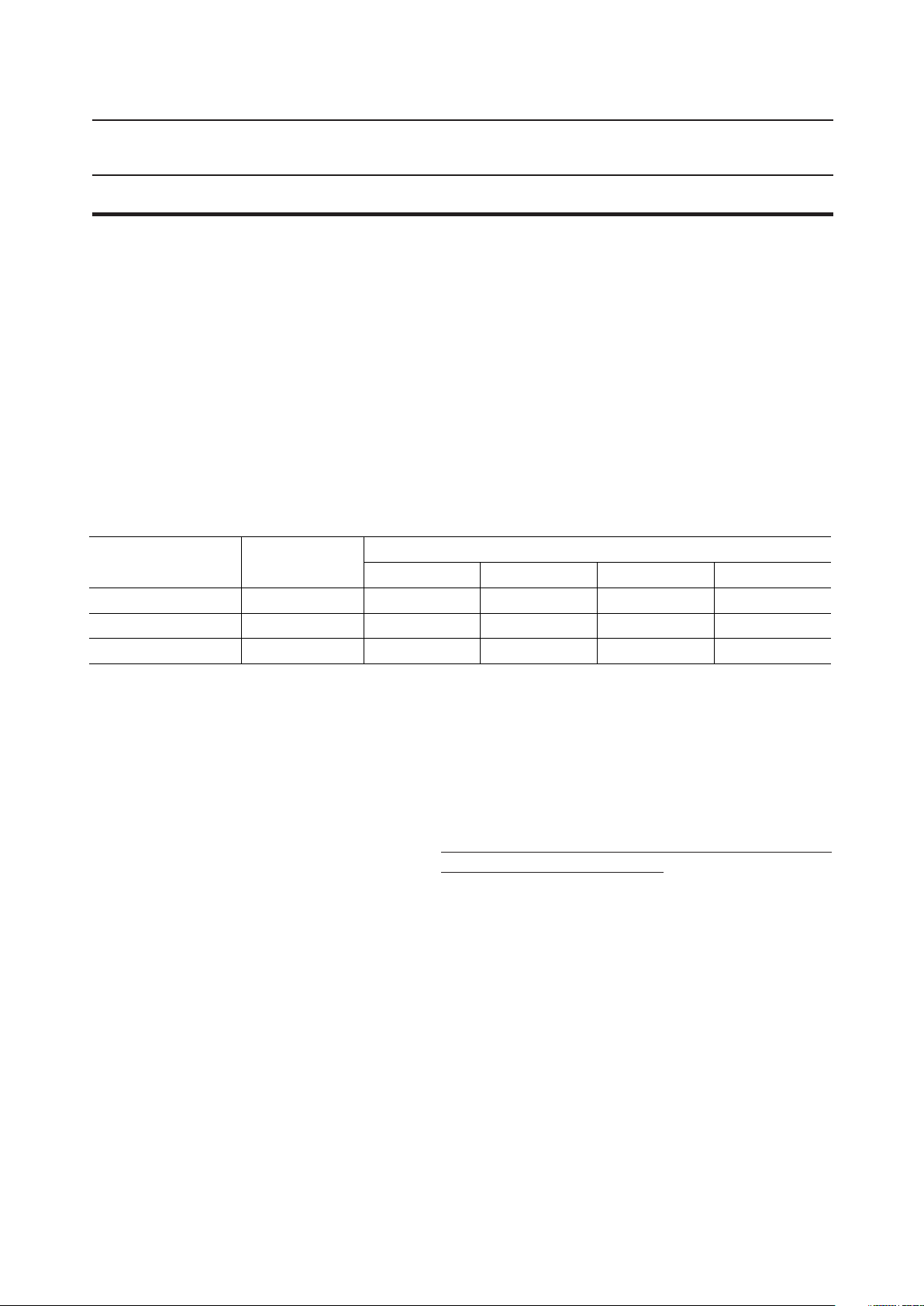
Device
MSM9802
MSM9803
MSM9805
* Actual voice ROM area is smaller by 11 Kbits.
• ROM custom
• 8-bit OKI nonlinear PCM method/8-bit straight PCM method
• Built-in edit ROM
• Random playback function
• Sampling frequency : 4.0 kHz/5.3 kHz/6.4 kHz/8.0 kHz/10.6 kHz/12.8 kHz/
• Maximum number of phrases : 63 (Microcontroller interface mode)
• Built-in current mode 10-bit D/A converter
• Built-in low-pass filter
• Standby function
• RC oscillation (256 kHz)/ceramic oscillation (4.096 MHz) selectable
• Package options:
18-pin plastic DIP (DIP18-P-300-2.54) (Product name: MSM9802-xxxRS/MSM9803-xxxRS/
24-pin plastic SOP (SOP24-P-430-1.27-K) (Product name: MSM9802-xxxGS-K/MSM9803-xxxGS-K/
30-pin plastic SSOP (SSOP30-P-56-0.65-K) (Product name: MSM9802-xxxGS-AK/MSM9803-xxxGS-
Chip
ROM size*
512 Kbits 16.0 10.0 8.0 4.0
1 Mbit 32.4 20.2 16.2 8.1
2 Mbits 65.1 40.7 32.5 16.2
=4.0 kHz f
f
SAM
16.0 kHz
Note: If RC oscillation is selected, 10.6 kHz, 12.8 kHz, and
16.0 kHz cannot be selected.
56 (Stand-alone mode)
Speech period (sec)
=6.4 kHz f
SAM
MSM9805-xxxRS)
MSM9805-xxxGS-K)
AK/MSM9805-xxxGS-AK)
=8.0 kHz f
SAM
xxx indicates code number.
=16.0 kHz
SAM
Note: This data sheet explains a stand-alone mode and a microcontroller interface mode,
separately.
1/51
Page 2

MSM9802/03/05-xxx¡ Semiconductor
CONTENTS
(1) Stand-alone Mode
BLOCK DIAGRAM ............................................................................................................................. 3
PIN CONFIGURATION ..................................................................................................................... 4
PIN DESCRIPTIONS ........................................................................................................................... 6
ABSOLUTE MAXIMUM RATINGS ................................................................................................. 8
RECOMMENDED OPERATING CONDITIONS ........................................................................... 8
ELECTRICAL CHARACTERISTICS ................................................................................................ 9
TIMING DIAGRAMS ....................................................................................................................... 12
FUNCTIONAL DESCRIPTION....................................................................................................... 14
1. Playback Code Specification ............................................................................................. 14
2. Pull-up/Pull-down Resistor .............................................................................................. 14
3. Stand-alone Mode ............................................................................................................... 14
APPLICATION CIRCUITS .............................................................................................................. 19
(2) Microcontroller Interface Mode
BLOCK DIAGRAM ........................................................................................................................... 21
PIN CONFIGURATION ................................................................................................................... 22
PIN DESCRIPTIONS ......................................................................................................................... 24
ABSOLUTE MAXIMUM RATINGS ............................................................................................... 25
RECOMMENDED OPERATING CONDITIONS ......................................................................... 25
ELECTRICAL CHARACTERISTICS .............................................................................................. 26
TIMING DIAGRAMS ....................................................................................................................... 29
FUNCTIONAL DESCRIPTION....................................................................................................... 31
1. Playback Code Specification ............................................................................................. 31
2. Address Data ....................................................................................................................... 31
3. Stop Code ............................................................................................................................. 32
4. Generating Pseudo - BUSY Signal through NAR pin .................................................... 33
APPLICATION CIRCUIT................................................................................................................. 34
(3) Common
1. Sampling Frequency ........................................................................................................... 35
2. Recording/Playback Time................................................................................................. 35
3. Playback Method ................................................................................................................ 36
4. Phrase Control Table ..........................................................................................................37
5. RC Oscillation ...................................................................................................................... 39
6. Ceramic Oscillation ............................................................................................................ 40
7. Low-pass Filter .................................................................................................................... 42
8. Standby Transition.............................................................................................................. 43
9. Voice Output Unit Equivalent Circuit (AOUT, V
Pins) .......................................... 44
REF
D/A CONVERTER CURRENT CHARACTERISTICS ................................................................ 45
PAD CONFIGURATION ................................................................................................................. 46
2/51
Page 3
3/51
MSM9802/03/05-xxx¡ Semiconductor
(1) STAND-ALONE MODE (CPU/STD: "L" level)
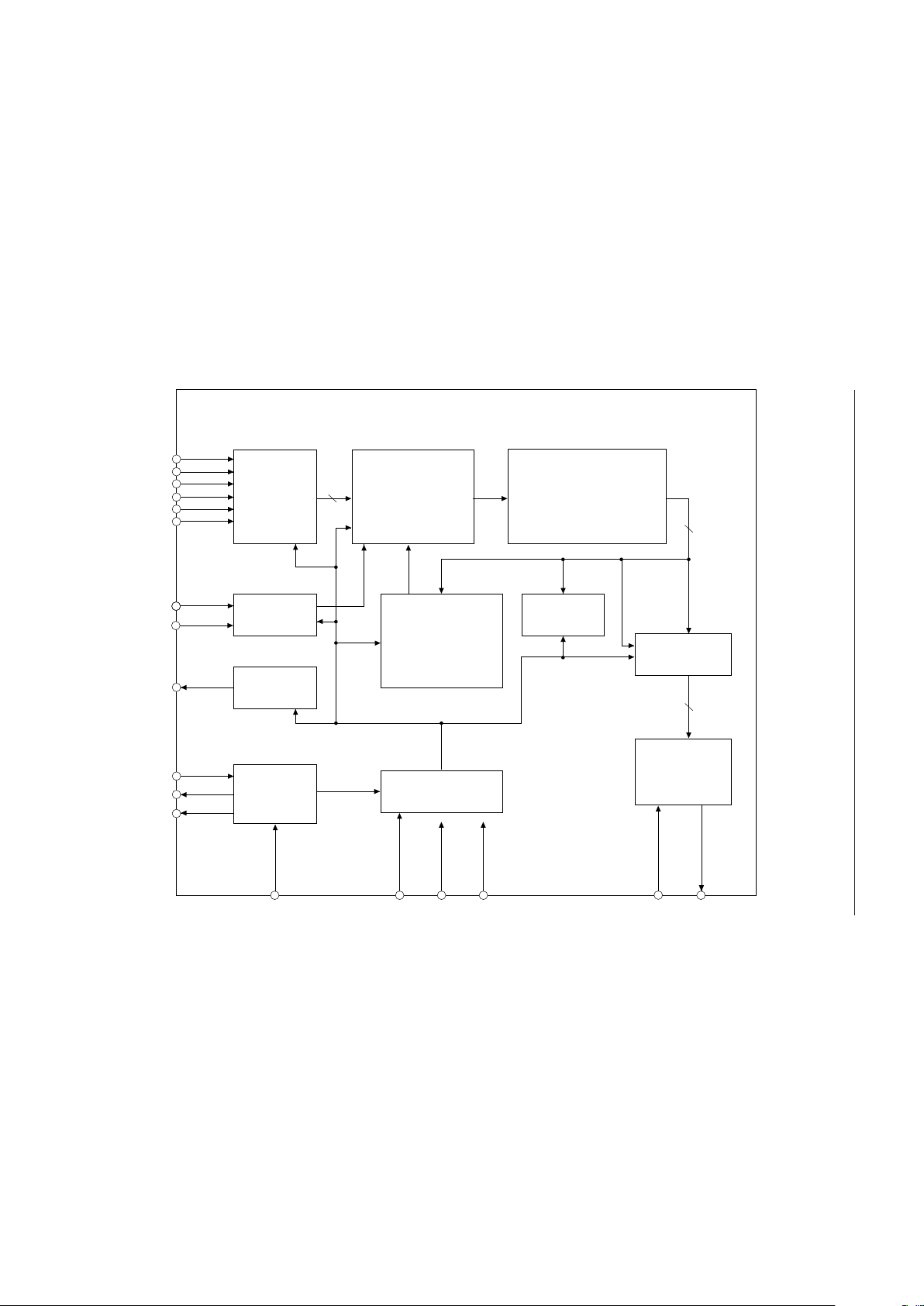
BLOCK DIAGRAM
512-Kbit (MSM9802)
1-Mbit (MSM9803)
2-Mbit (MSM9805)
Multiplexer
Address &
Switching
Controller
6
PCM
Synthesizer
10
8
10-Bit
DAC
&
LPF
AOUT
DATA
Controller
16-Bit (MSM9802)
17-Bit (MSM9803)
18-Bit (MSM9805)
Timing Controller
GNDV
DD
RESET
Random
Circuit
I/O
Interface
OSC
XT/RC
XT/CR
A2
A1
A0
SW2
SW1
SW0
RND
BUSY
OSC1
OSC2
OSC3/TEST
CPU/STD
V
REF
16-Bit (MSM9802)
17-Bit (MSM9803)
18-Bit (MSM9805)
Address Counter
ROM
(Including 11 Kbits of
Edit ROM & Address ROM)
Page 4
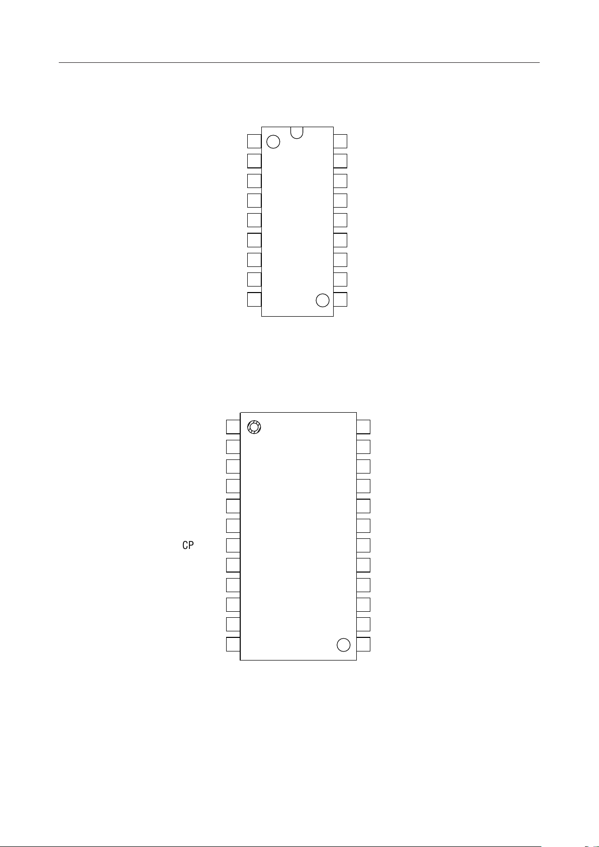
PIN CONFIGURATION (TOP VIEW)
MSM9802/03/05-xxx¡ Semiconductor
A0
A1
A2
RESET
XT/CR
BUSY
GND
V
REF
AOUT
1
2
3
4
5
6
7
8
9
18
SW2
17
SW1
16
SW0
15
RND
14
CPU/STD
13
OSC3/TEST
12
OSC2
11
OSC1
10
V
DD
18-Pin Plastic DIP
Note: Applicable to MSM9802-xxxRS, MSM9803-xxxRS, and MSM9805-xxxRS.
V
1
DD
24
AOUT
23
22
21
20
19
18
17
16
15
14
13
NC
NC
RND
NC
SW0
SW1
SW2
2
3
4
5
6
7
8
9
10
11
12
OSC1
OSC2
OSC3/TEST
CPU/STD XT/CR
NC: No connection
24-Pin Plastic SOP
V
REF
GND
NC
BUSY
NC
RESET
NC
A2
A1
A0
Note: Applicable to MSM9802-xxxGS-K, MSM9803-xxxGS-K, and MSM9805-xxxGS-K.
4/51
Page 5
MSM9802/03/05-xxx¡ Semiconductor
V
DD
OSC1
OSC2
NC
NC
OSC3/TEST
NC
CPU/STD
NC
RND
NC
SW2
30
29
28
27
26
25
24
23
22
21
20
16
AOUT
V
GND
NC
NC
BUSY
NC
XT/CR
NC
RESET
NC
A0
1
2
3
4
5
6
7
8
9
10
11
12 19NC NC
13 18SW0 A2
14 17SW1 A1
15
REF
NC: No connection
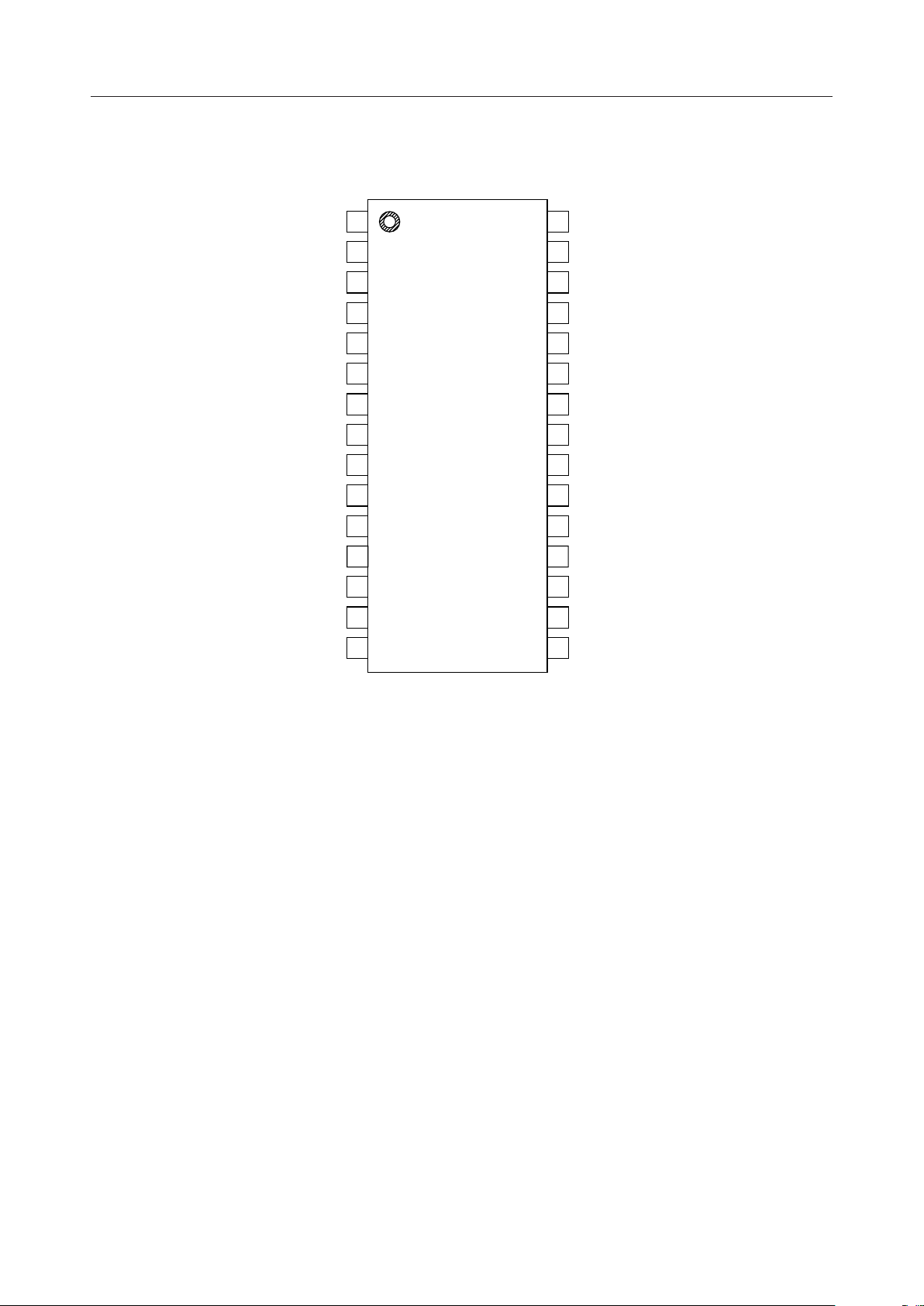
30-Pin Plastic SSOP
Note: Applicable to MSM9802-xxxGS-AK, MSM9803-xxxGS-AK, and MSM9805-xxxGS-AK.
5/51
Page 6
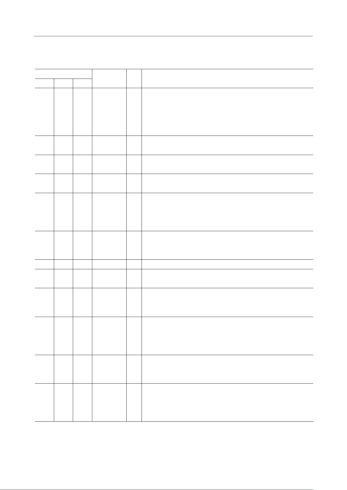
PIN DESCRIPTIONS
MSM9802/03/05-xxx¡ Semiconductor
Pin
DIP4SOP17SSOP
21
62025
51823
14 7 8
82329
92430
72228
10 1 1
11 2 2
12 3 3
13 5 6
15810
Symbol Type Description
The IC enters the standby state if this pin is set to "L" level. At this time,
oscillation stops and AOUT drives a current of 0mA and becomes GND
RESET I
level, then the IC returns to the initial state.
Apply a "L" pulse upon power-on.
This pin has an internal pull-up resistor.
Outputs "L" level while voice is being played back.
BUSY O
At power-on, this pin is at "H" level.
XT/RC switching pin. Set to "H" level if ceramic oscillation is used.
XT/CR I
Set to "L" level if RC oscillation is used.
Microcontroller interface/stand-alone mode switching pin.
CPU/STD I
Set to "L" level if the MSM9802/03/05 is used in stand-alone mode.
Volume setting pin. If this pin is set to GND level, the maximum
current is forced in. If this pin is set to V
V
REF
I
is forced in. A pull-down resistor of approx. 10 W is internally
connected to this pin during operation.
Voice output pin.
AOUT O
The voice signals are output as current changes. In standby state, this
pin drives a current of 0 mA and becomes GND level.
GND —
Ground pin.
Power supply pin. Insert a bypass capacitor of 0.1 mF or more between
V
DD
—
and GND pins.
V
DD
Ceramic oscillator connection pin when ceramic oscillation is selected.
OSC1 I
RC connection pin when RC oscillation is selected.
Input from this pin if external clock is used.
Ceramic oscillator connection pin when ceramic oscillation is selected.
RC connection pin when RC oscillation is selected.
OSC2 O
Leave this pin open if external clock is used.
Outputs "L" level in standby state.
Leave this pin open when ceramic oscillation is used.
OSC3/TEST O
RC connection pin when RC oscillation is selected.
Outputs "H" level in standby state when RC oscillation is selected.
Random playback starts if RND pin is set to "L" level.
Fetches addresses from random address generation circuit in the IC at
RND I
fall of RND. Set to "H" level when the random playback function is not
used. This pin has internal pull-up resistor.
level, the minimum current
DD
6/51
Page 7

MSM9802/03/05-xxx¡ Semiconductor
Pin
DIP SOP SSOP
16-18 10-12 13-15
1-3 13-15 16-18
Symbol Type Description
Phrase input pins corresponding to playback sound.
SW0 - SW2 I
A0 - A2 I
If input changes, SW0 to SW2 pins fetch addresses after 16 ms and
start voice synthesis.
Each of these pins has internal pull-down resistor.
Phrase input pins corresponding to playback sound.
Input logic of A0 pin becomes invalid if the random playback function
is used.
7/51
Page 8
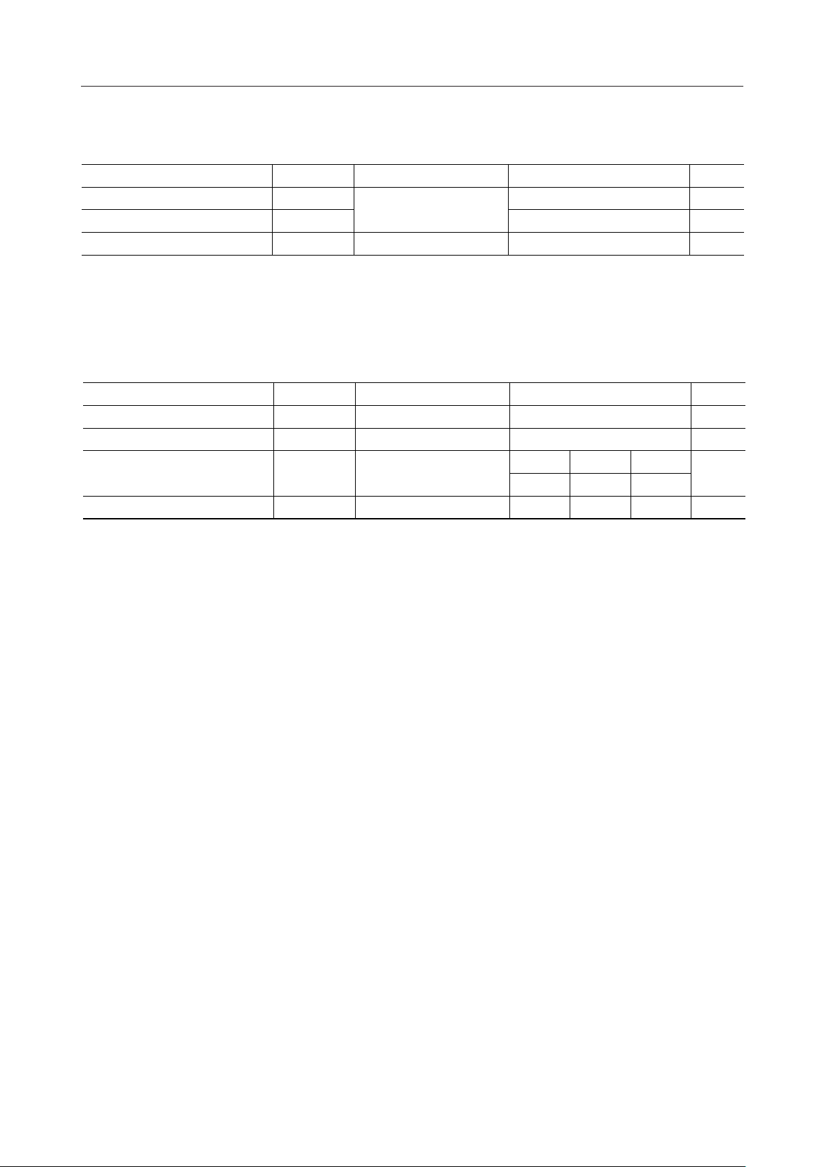
ABSOLUTE MAXIMUM RATINGS
Parameter Symbol Condition Rating Unit
Power Supply Voltage
Input Voltage
Storage Temperature
T
V
V
DD
IN
STG
Ta=25°C
RECOMMENDED OPERATING CONDITIONS
Parameter Symbol Condition Range Unit
Power Supply Voltage V
Operating Temperature —
Master Clock Frequency 1
T
f
OSC1
OSC2
DD
op
— 2.0 to 5.5 V
MSM9802/03/05-xxx¡ Semiconductor
–0.3 to +7.0 V
–0.3 to VDD+0.3 V
–55 to +150 °C—
–40 to +85 °C
Min. Max.
Typ.
4.0963.5 4.5
256200 300Master Clock Frequency 2 f
(GND=0 V)
(GND=0 V)
MHzWhen crystal is selected
kHzWhen RC is selected (*1)
*1 The accuracy of the oscillation frequency when RC oscillation is selected depends largely on
the accuracy of the external R and C.
8/51
Page 9
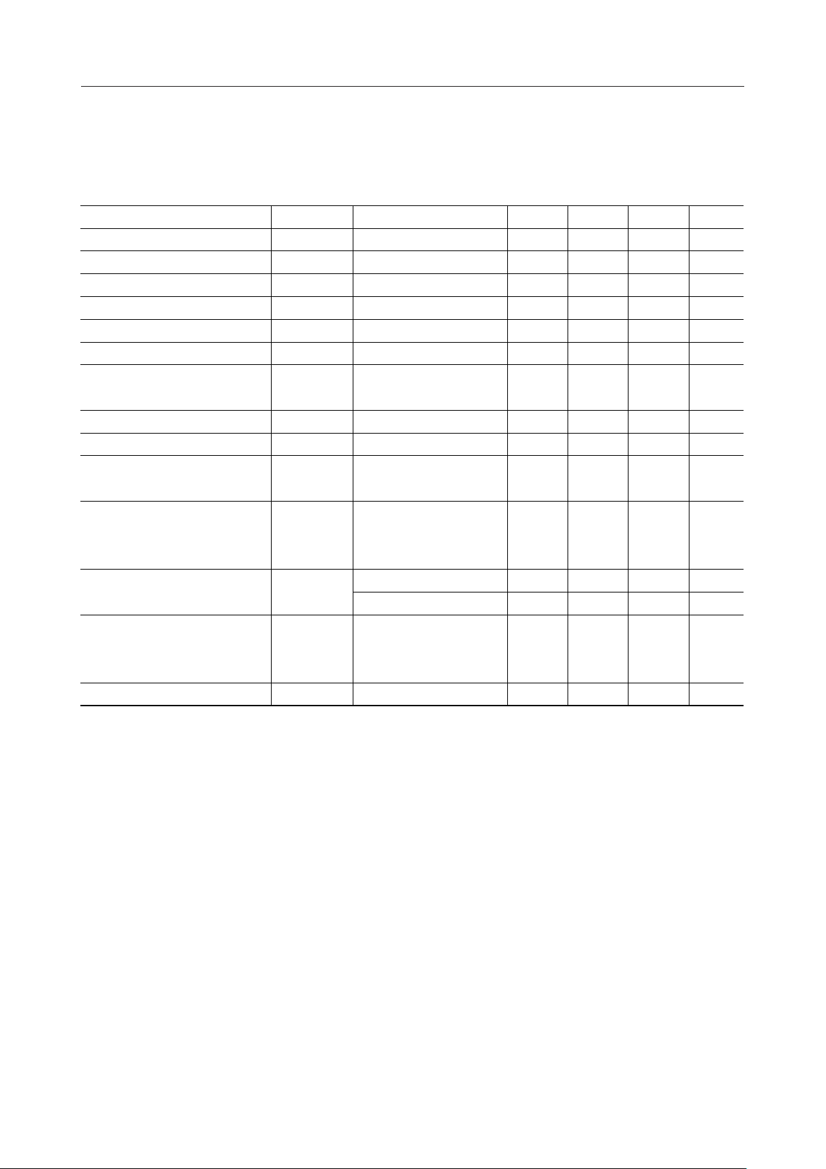
ELECTRICAL CHARACTERISTICS
DC Characteristics
(V
=5.0 V, GND=0 V, Ta=–40 to +85°C, unless otherwise specified)
DD
Parameter Symbol Condition Unit
"H" Input Voltage V
"L" Input Voltage —
*1
*2
*3
*4
Standby Current I
V
Pin Pull-down Resistance
REF
IH
V
IL
V
OH
V
OL
IH1
Internal pull-down resistor
Applies to OSC1 pin only.
I
IH2
IH3
IL1
IL2
V
DD1
AOUT bias voltage=0V
At maximum output current
DD2
V
AOUT bias voltage=0V
DS
At maximum output current,
AOUT
V
AOUT bias voltage=0V
R
VREF
MSM9802/03/05-xxx¡ Semiconductor
Min. Max.
——V
4.2 —
— 0.8
4.6 —
DD
V
IH=VDD
REF=VDD
REF
REF
,
=GND,
=GND,
Typ.
—V
—V"H" Output Voltage IOH=–1 mA
—— 0.4
——10"H" Input Current 1 I
9030 200"H" Input Current 2 I
——15"H" Input Current 3
—–10 —"L" Input Current 1 I
–90–200 –30"L" Input Current 2 I
0.4—1Dynamic Supply Current 1 I
——16Dynamic Supply Current 2 I
V"L" Output Voltage IOL=2 mA
µAVIH=V
µA
µA
µAVIL=GND
µAInternal pull-up resistor
mA
mA
——10µATa=–40 to +70°C
——50
9.5615AOUT Output Current I
10713
µATa=70 to 85°C
mA
kW—
*1 Applicable to SW0-SW2
*2 Applicable to RESET, RND
*3 Dynamic supply current (excluding DAC output current)
*4 Dynamic supply current at maximum output current
9/51
Page 10
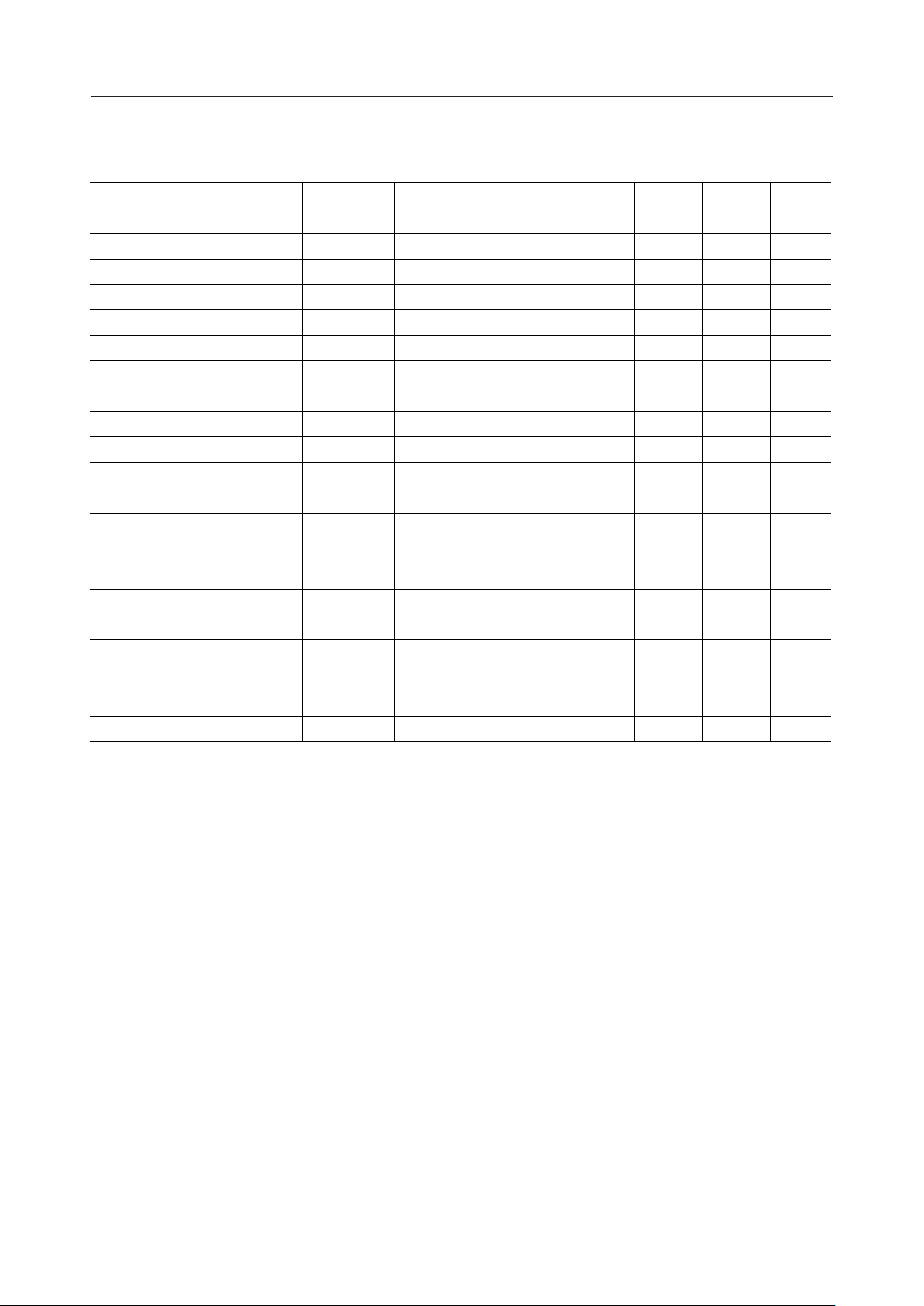
DC Characteristics
(V
=3.1 V, GND=0 V, Ta=–40 to +85°C, unless otherwise specified)
DD
Parameter Symbol Condition Unit
"H" Input Voltage V
"L" Input Voltage —
*1
*2
*3
*4
Standby Current I
V
Pin Pull-down Resistance
REF
IH
V
IL
V
OH
V
OL
IH1
IH2
Internal pull-down resistor
Applies to OSC1 pin only.
IH3
IL1
IL2
V
DD1
AOUT bias voltage=0V
At maximum output current
I
DD2
V
AOUT bias voltage=0V
DS
At maximum output current,
AOUT
V
AOUT bias voltage=0V
R
VREF
MSM9802/03/05-xxx¡ Semiconductor
Min. Max.
——V
2.7 —
— 0.5
2.6 —
DD
V
IH=VDD
REF=VDD
REF
REF
,
=GND,
=GND,
Typ.
—V
—V"H" Output Voltage IOH=–1 mA
—— 0.4
——10"H" Input Current 1 I
3010 100"H" Input Current 2 I
——15"H" Input Current 3 I
—–10 —"L" Input Current 1 I
–30–100 –10"L" Input Current 2 I
0.15— 0.5Dynamic Supply Current 1 I
—— 5.5Dynamic Supply Current 2
V"L" Output Voltage IOL=2 mA
µAVIH=V
µA
µA
µAVIL=GND
µAInternal pull-up resistor
mA
mA
——5µATa=–40 to +70°C
——20
3.21.4 5AOUT Output Current I
10713
µATa=70 to 85°C
mA
kW—
*1 Applicable to SW2-SW0
*2 Applicable to RESET, RND
*3 Dynamic supply current (excluding DAC output current)
*4 Dynamic supply current at maximum output current
10/51
Page 11
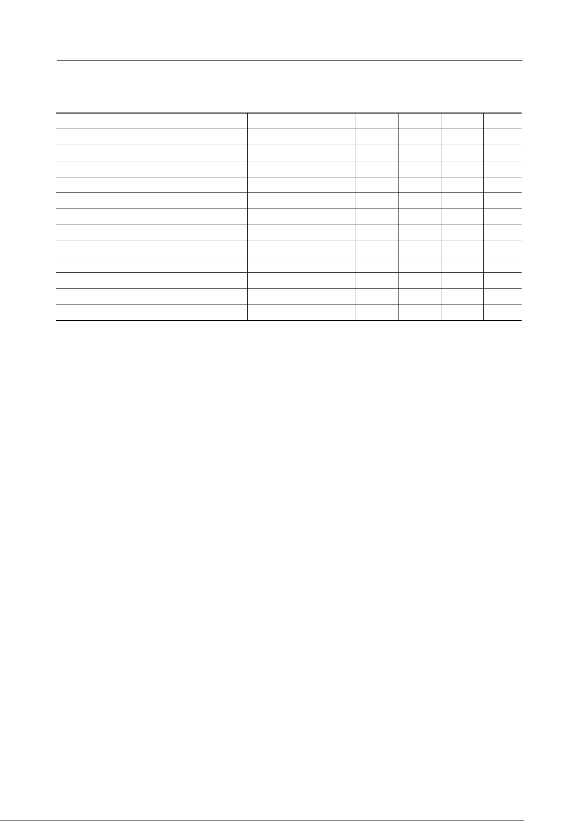
AC Characteristics
Parameter Symbol Condition Unit
Master Clock Duty Cycle f
RESET Input Pulse Width —
RESET Input Time After Power-on
BUSY
Output Time t
duty
t
w(RST)
t
D(RST)
t
w(RAN)
w(SW)
SBS
CHA
CHB
, t
DAR
DAF
STB
BLN
RA
f
MSM9802/03/05-xxx¡ Semiconductor
(V
=5.0 V, GND=0 V, Ta=–40 to +85°C)
DD
Min. Max.
—50%
40 60
10 —
—
0—
(note)
(note)
—
(note)
(note)
(note)
SAM
=8 kHz
(note)
(note)
Typ.
—µs
—µs
—100 —
—16 —SW0-SW2 Input Pulse Width t
——10
1514 16Chattering Prevention Time 1 t
——16Chattering Prevention Time 2 t
6460 68D/A Converter Change Time t
250200 300Standby Transition Time t
375350 500Silence Time Between Phrases t
1615 17Random Address Fetch Time t
µsRND Input Pulse Width —
ms—
µs—
ms—
ms
ms—
ms—
µs
µs—
(Note) Proportional to master the periods of oscillation frequencies f
The rated values show values when the standard master oscillation frequency is used.
OSC1
and f
OSC2
.
11/51
Page 12
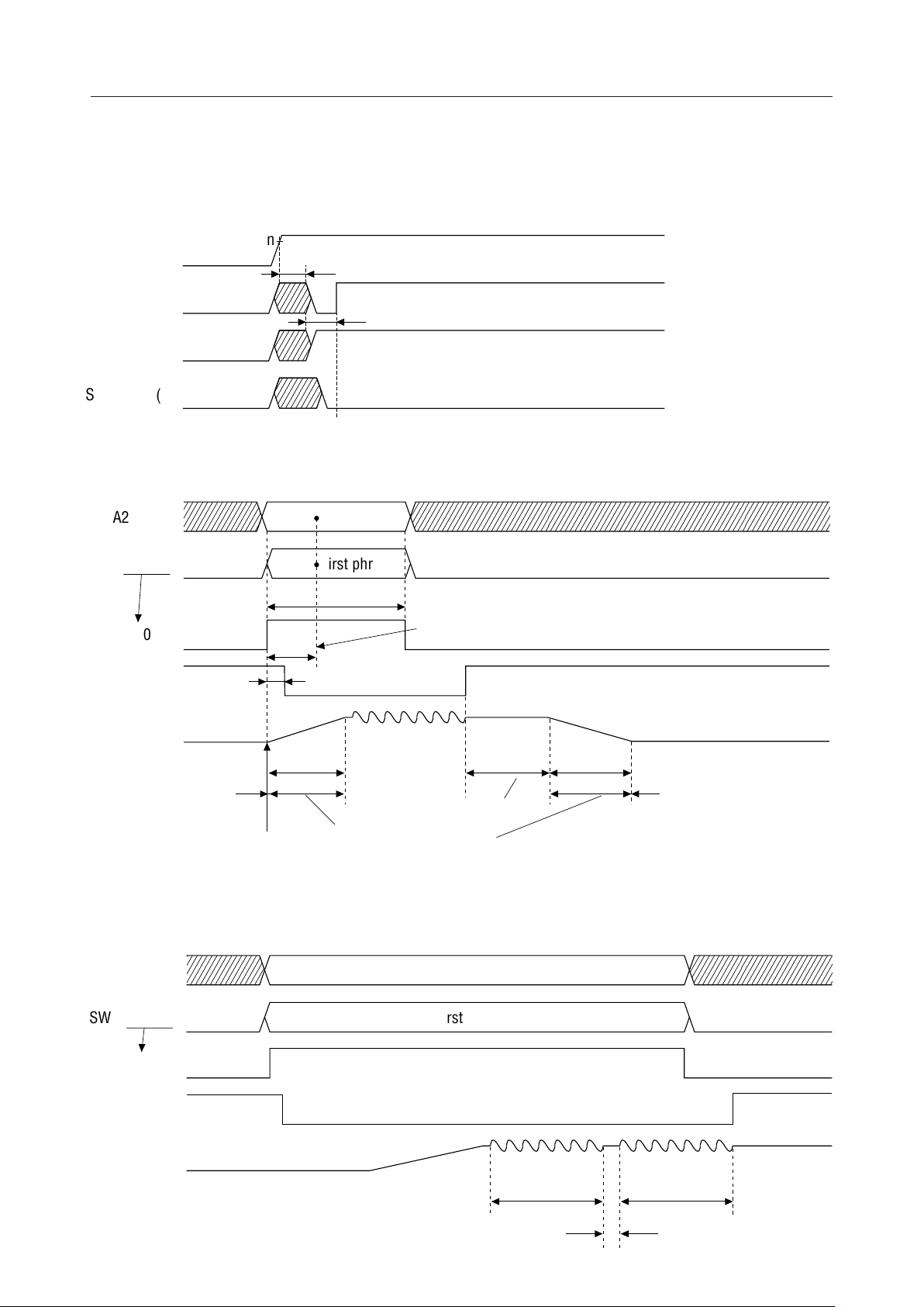
TIMING DIAGRAMS
AC Characteristics at Power-On
MSM9802/03/05-xxx¡ Semiconductor
V
DD
VDDMin
t
D(RST)
RESET (I)
t
W(RST)
BUSY (O)
SW2-SW0 (I)
AC Characteristics in Standby Status and when the IC is Activated
A2-A0 (I)
SW2-SW0 (I)
SW0 (I)
BUSY (O)
t
t
SBS
First phrase
First phrase"000" "000"
t
w(SW)
CHA
Address data fetch
AOUT (O)
t
DAR
Standby status
Oscillation start
Repeated Playback Timing
A2-A0 (I)
SW2-SW0 (I)
SW0 (I)
BUSY (O)
AOUT (O)
Standby transition time
D/A converter change time
First phrase
First phrase"000" "000"
t
STB
Single phrase
playback
t
DAF
Standby status
Single phrase
repeated playback
t
BLN
12/51
Page 13
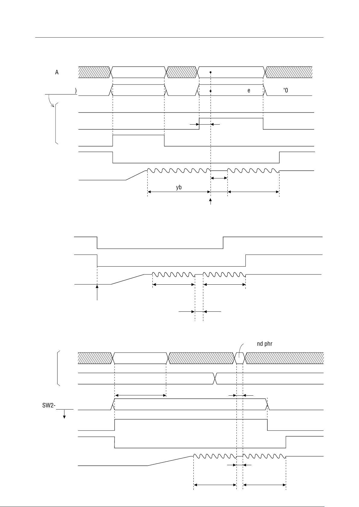
Timing when Changing from SW2 to SW0 During Playback
MSM9802/03/05-xxx¡ Semiconductor
A2-A0 (I)
SW2-SW0 (I)
SW2 (I) "L"
SW1 (I)
SW0 (I)
BUSY (O)
AOUT (O)
First phrase
First phrase"000" "000"
First phrase
playback
First phrase playback stops
t
CHB
Repeated Playback Timing for Random Playback
RND (I)
Second phrase
Second phrase "000"
t
BLN
Second phrase
playback
BUSY (O)
AOUT (O)
First phrase
playback
repeated playback
Oscillation start
Timing when Changing from A2 to A0 During Playback
A2-A0 (I)
SW2-SW0 (I)
(Ex.)
"000" "000"
SW0 (I)
First phrase
First phrase
t
CHA
First phrase
Same phrase
t
BLN
Second phrase
(Second phrase)
Second phrase
Address data fetch
BUSY (O)
AOUT (O)
First phrase
playback
t
BLN
Second phrase
playback
13/51
Page 14
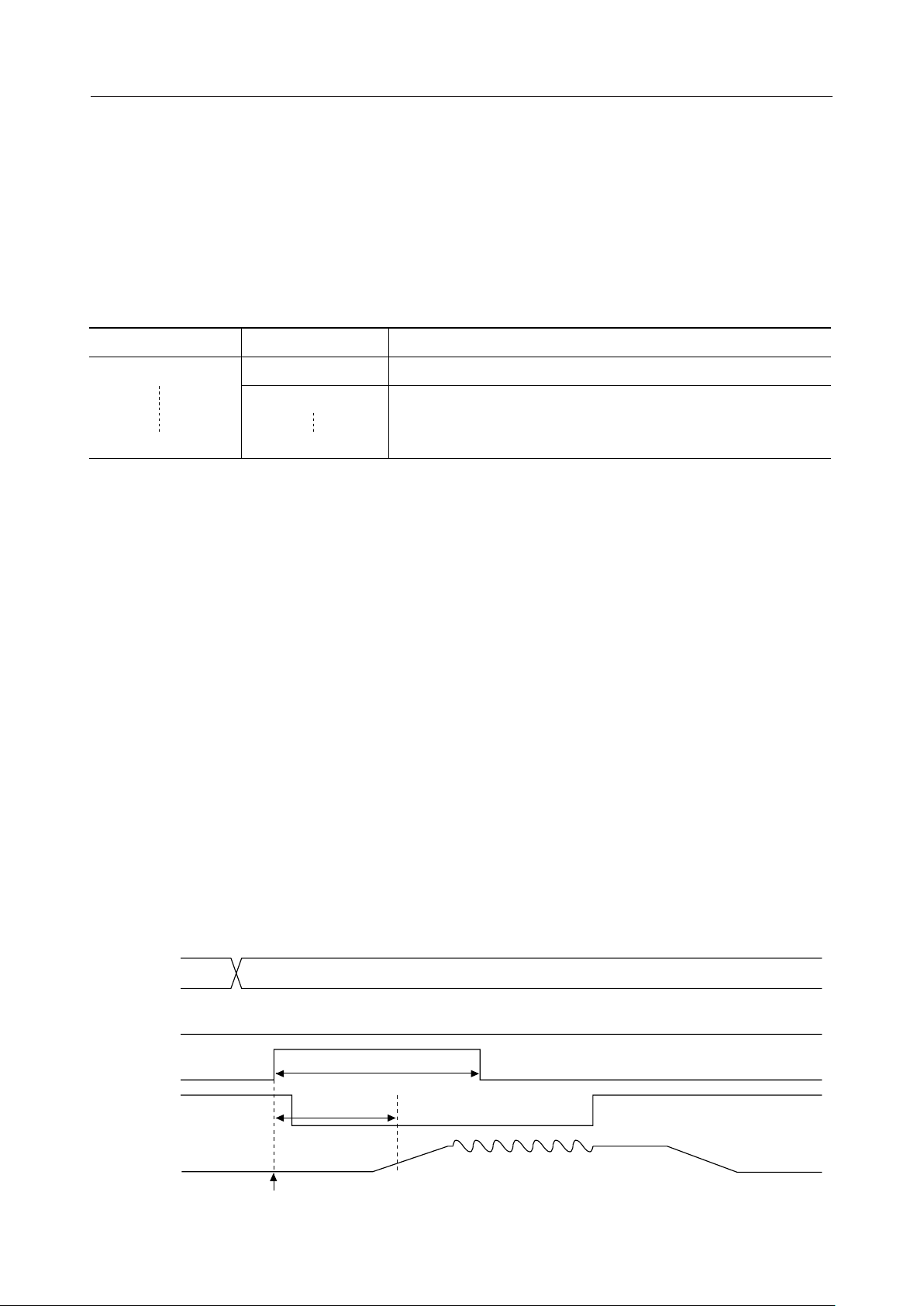
MSM9802/03/05-xxx¡ Semiconductor
FUNCTIONAL DESCRIPTION
1. Playback Code Specification
The user can specify a maximum of 56 phrases. Table 1.1 shows the settings by the A2-A0 and
SW2-SW0 pins.
Table 1.1 User-specified Phrases
A2-A0 Code Details
000
111
SW2-SW0
000
001
111
Inhibit code
User-specified phrase
(56 phrases)
2. Pull-up/Pull-down Resistor
The RESET and RND pins have internal pull-up resistors and the SW2-SW0 pins have internal
pull-down resistors.
3. Stand-alone Mode
In a stand-alone mode, the SW input interface function and the random playback function can
be used.
3.1 SW input interface
With the SW input interface, speech synthesis starts when the state of the SW2-SW0 pins has
changed. To prevent chattering, the address data is latched 16 ms (t
) after the state of SW2-
CHA
SW0 has changed. Voice synthesis does not start if the state of the A2-A0 pins has changed. Set
the RND pin to "H" level if the random playback function is not used.
Set the A2-A0 pins to "L" level at power-on or at reset.
The SW input interface is effective when the MSM9802/03/05 is operated using a push-button
switch. Voice synthesis starts when an address is changed by pressing the push-button switch.
If the push-button switch is released during playback, then playback stops after the current
phrase is completed.
A2-A0 (I)
SW2-SW1 (I) "L"
t
CHA
t
w(SW)
SW0 (I)
BUSY (O)
AOUT (O)
Oscillation start
Figure 3.1 SW Input Interface Single-Phrase Playback Timing
14/51
Page 15
MSM9802/03/05-xxx¡ Semiconductor
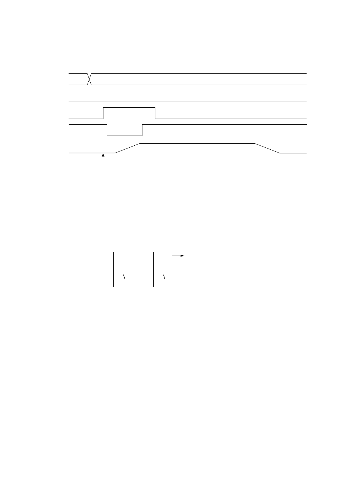
If playback is attempted at an unused address in the phrases, AOUT goes to 1/2 I
AOUT
and
playback does not occur. Figure 3.2 shows the timing.
A2-A0 (I)
SW2-SW1 (I) "L"
SW0 (I)
BUSY (O)
AOUT (O)
Oscillation start
Figure 3.2 Timing when Playback is Attempted at an Unused Phrase Address
In the SW input interface, no phrase is triggered when SW2 to SW0 are all set to "0". Therefore,
when the circuit consists of a diode matrices that use push-button switches, the maximum
playback phrases are 56 phrases.
A2-A0
000
001
002
111
8 codes
SW2-SW0
¥
¥
(000)
001
002
111
7 codes
Code Prohibited
= 56 Phrases
= 56
3.2 Random playback function
The random playback function randomly generates 15 different addresses corresponding to the
four bits of the addresses of A0 and SW2-SW0 (except ALL "L") on the IC, after which playback
commences.
Therefore, any input to A0 and SW2 to SW0 pins from external control is invalid. Hold these 4
pins either "H" or "L" level. SW2 to SW0 pins may be held open as they have internal pull-down
resistor.
Playback may not occur if all the 15 addresses have not been assigned a phrase. Care must be
taken when creating ROM data.
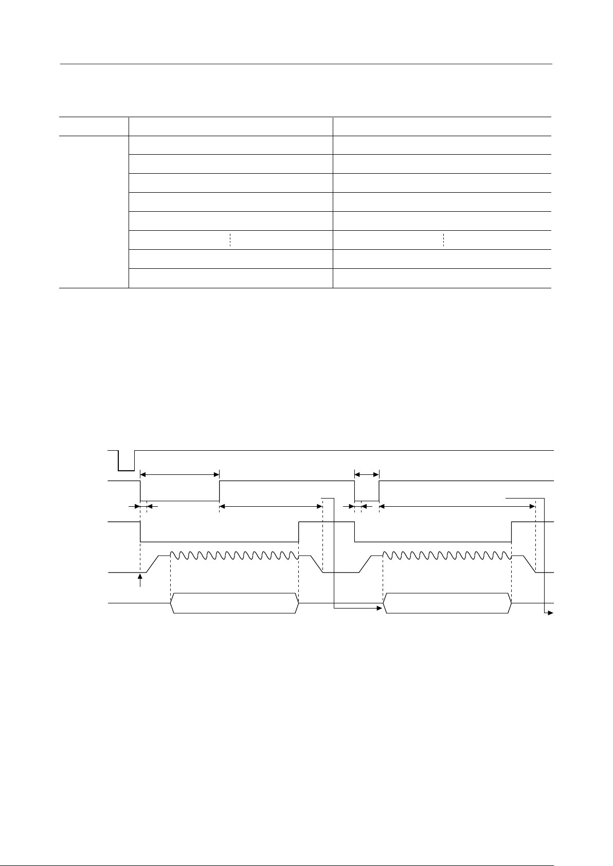
For example, when four phrases, "sunny", "rainy", "cloudy", and "snowy", are to be played
randomly, set the phrases as shown in Table 3.1 in which a phrase is assigned to all the 15
addresses. The four phrases are then played back at random as shown below.
15/51
Page 16
MSM9802/03/05-xxx¡ Semiconductor
Table 3.1 Random Address Setup Example
A2, A1 A0, SW2-SW0 Phrase
00 0001
0010
0011
0100
0101
1110
1111
sunny
rainy
cloudy
snowy
sunny
rainy
snowy
Random playback starts when the timing shown in Figure 3.3 is input to the RND pin. A random
address is fixed based on the "H" level time of the RND pin during IC oscillation. Random
address is captured at the fall of the RND pin, and voice playback commences. Therefore, when
power is turned on, or when RESET is input, the phrase at fixed address "0001" is played while
the random counter remains initialized until random playback is initiated.
RESET (I)
RND (I)
BUSY (O)
AOUT (O)
Oscillation start
t
W (RAN)
t
RA
t
W (RAN)
Random address fixed time Random address fixed time
t
RA
Playback
(Address = 0001)
Playback
(Address = random)
Figure 3.3 Random Address Capture
16/51
Page 17
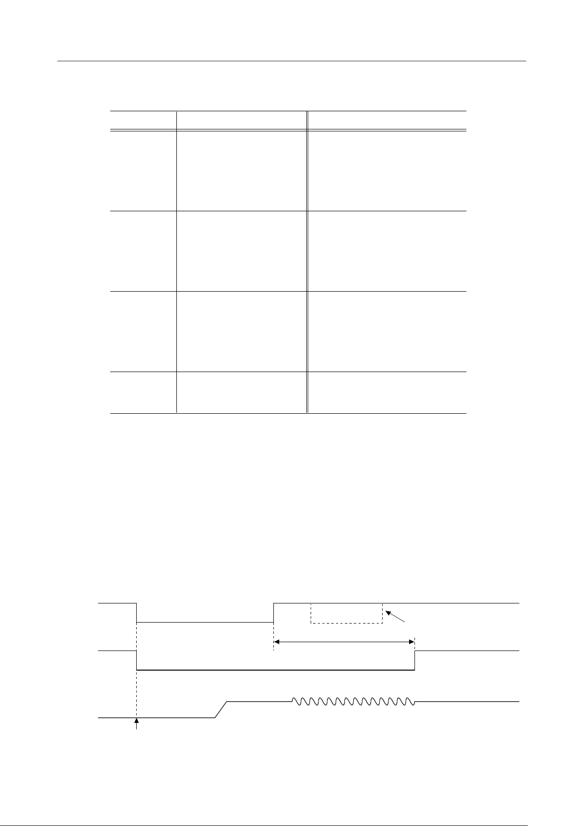
Table 3.2 Random Playback Address
A2, A1 A0, SW2 to SW0 Phrase (Sample)
MSM9802/03/05-xxx¡ Semiconductor
00
01
10
11
0001
0010
0011
0100
1111
0001
0010
0011
0100
1111
0001
0010
0011
0100
1111
0001
1111
··· ··· ··· ···
Hit
Hit
Hit
Out
Out
Hit
Out
Out
Out
Out
White
Black
Red
Blue
··· ··· ···
Green
··· ······
For a random address, 15 phrases can be set for each logical condition of addresses A2 and A1
(i.e., "00", "01", "10", and "11").
In random playback, the four logic states ("000000", "010000", "100000" and "110000") in userspecified phrases cannot be used. Take it into consideration when creating ROM data.
A random address is set by the "H" level time of the RND pin, so if the same pulse width is input
by microcontroller, the random address fixed time becomes constant, and a random phrase may
not be played under these conditions. The random address fixed time must be inconsistent in
order to produce random playback.
RND (I)
Invalid pulse
Pulse input during this time period is invalid
BUSY (O)
AOUT (O)
Oscillation start
Figure 3.4 Timing when a Pulse is Input to the RND Pin During Random Playback
17/51
Page 18
MSM9802/03/05-xxx¡ Semiconductor
Table 3.3 Random Playback and Stop Address
A2, A1 A0, SW2-SW0* Code Details
0001
00
1111
01 0001 Stop address
Random playback address
* Address(es) corresponding to the A0 and SW2-SW0 pins
SW0
SW1
SW2
A0
A1
A2
RND
(15 addresses)
Figure 3.5 Circuit Example for Random Playback Stop
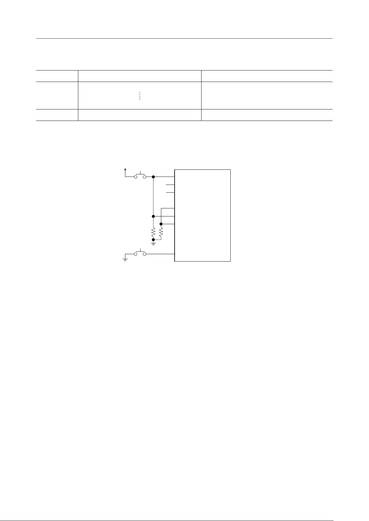
An unused user-specified address is used as a stop address, therefore the IC can enter standby
without voice playback, as shown in Figure 3.2.
18/51
Page 19
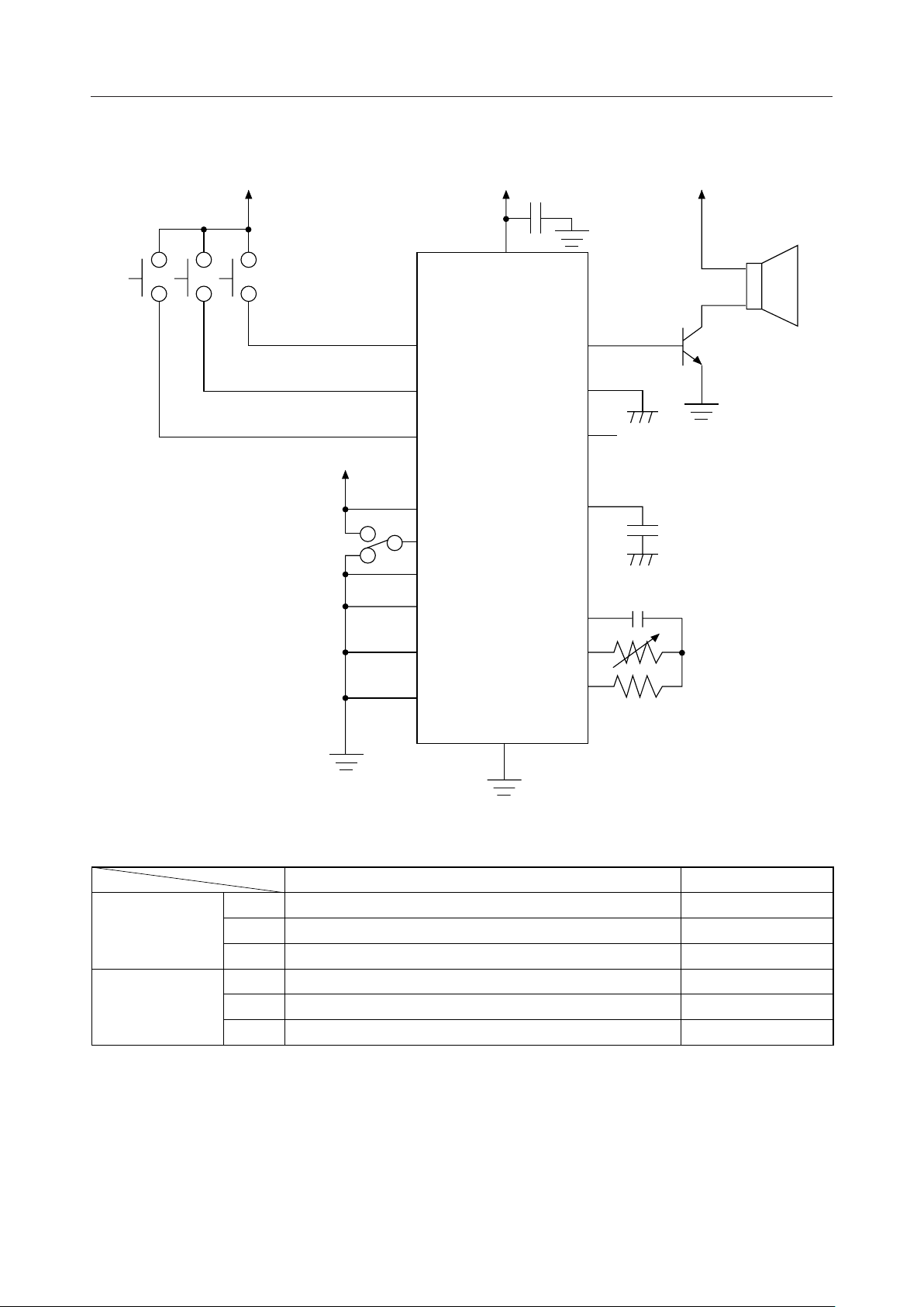
APPLICATION CIRCUITS
S3 S2 S1
MSM9802/03/05-xxx¡ Semiconductor
V
DD
S4
SW0
SW1
SW2
RND
A0
A1
A2
XT/CR
CPU/STD
GND
AOUT
V
REF
BUSY
RESET
OSC3
OSC2
OSC1
S4="L"
S4="H"
Address [HEX]SW0SW1SW2A0A1A2
100000S1
010000S2
001000S3
100100S1
010100S2
001100S3
Application Circuit for Playing Six Phrases Using Four Switches
01
02
04
09
0A
0C
19/51
Page 20
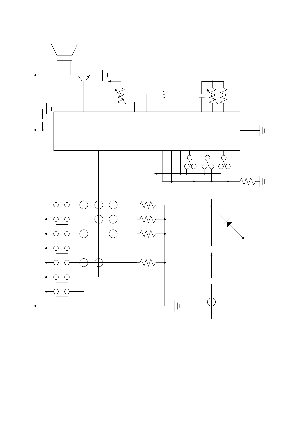
V
DD
AOUT
SW0
SW1
SW2
REF
V
BUSY
RESET
XT/CR
CPU/STD
RND
A0
OSC3
A1
MSM9802/03/05-xxx¡ Semiconductor
OSC2
OSC1
GND
A2
1234567
Application Circuit Using Switches
20/51
Page 21
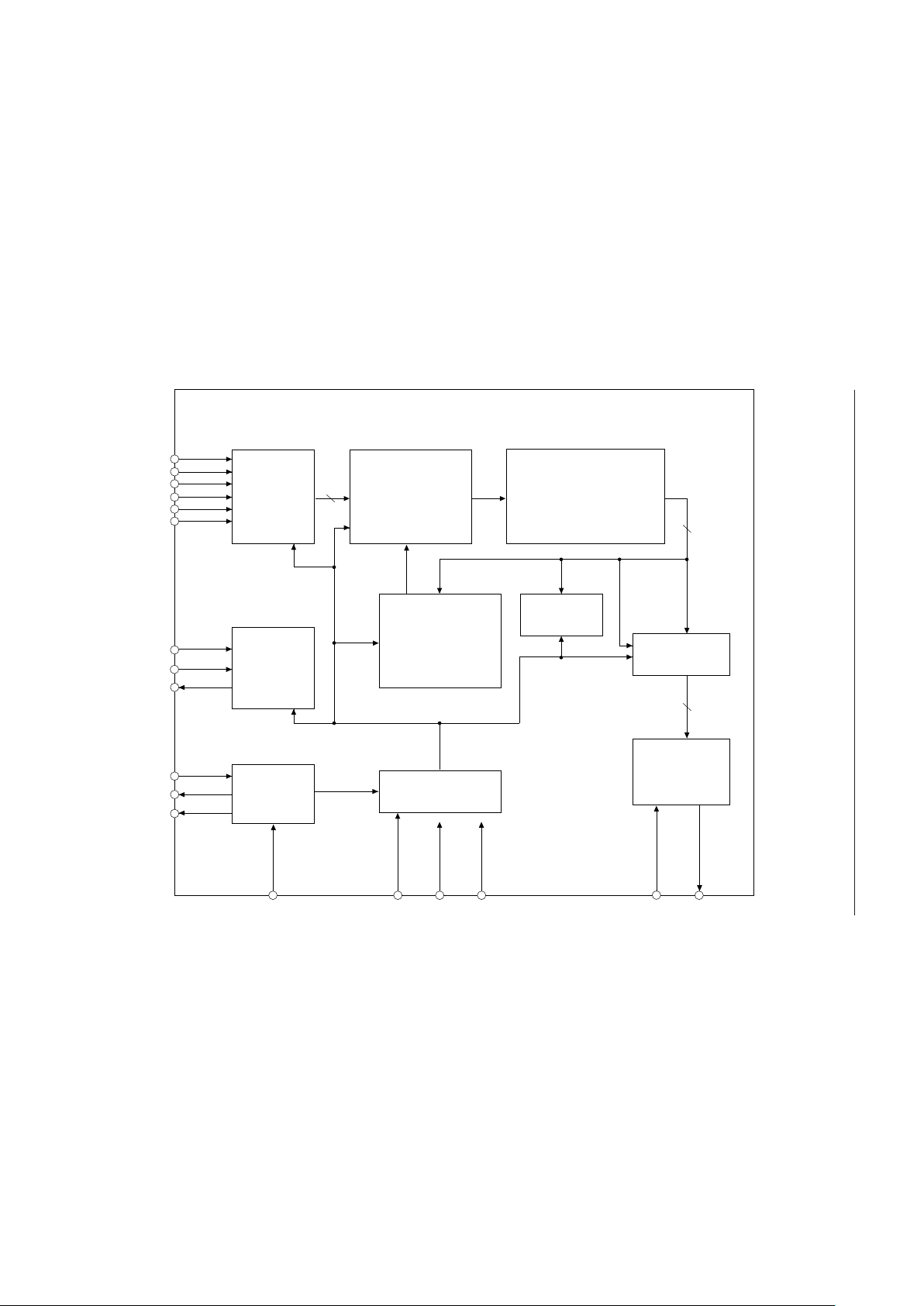
21/51
MSM9802/03/05-xxx¡ Semiconductor
(2) MICROCONTROLLER INTERFACE MODE (CPU/STD: "H" level)
BLOCK DIAGRAM
ROM
(Including 11Kbit of
Edit ROM & Address ROM)
Multiplexer
Address
Controller
6
PCM
Synthesizer
10
8
10-Bit
DAC
&
LPF
AOUT
DATA
Controller
Address Counter
Timing Controller
GNDV
DD
RESET
I/O
Interface
OSC
XT/RC
XT/CR
I5
I4
I3
I2
I1
I0
ST
NAR
OSC1
OSC2
OSC3/TEST
CPU/STD
V
REF
512-Kbit (MSM9802)
1-Mbit (MSM9803)
2-Mbit (MSM9805)
16-Bit (MSM9802)
17-Bit (MSM9803)
18-Bit (MSM9805)
16-Bit (MSM9802)
17-Bit (MSM9803)
18-Bit (MSM9805)
Page 22
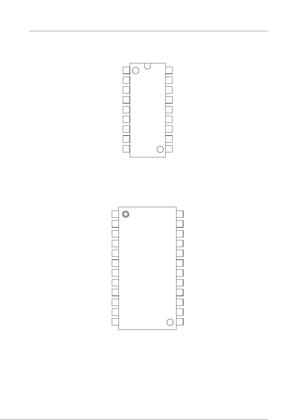
PIN CONFIGURATION (TOP VIEW)
MSM9802/03/05-xxx¡ Semiconductor
RESET
XT/CR
NAR
GND
V
REF
AOUT
I3
I4
I5
1
2
3
4
5
6
7
8
9
18
I2
17
I1
16
I0
15
ST
14
CPU/STD
13
OSC3/TEST
12
OSC2
11
OSC1
10
V
DD
18-Pin Plastic DIP
Note: Applicable to MSM9802-xxxRS, MSM9803-xxxRS, and MSM9805-xxxRS.
V
1
DD
24
AOUT
23
22
21
20
19
18
17
16
15
14
13
V
REF
GND
NC
NAR
NC
XT/CR
RESET
NC
I5
I4
I3
OSC1
OSC2
NC
OSC3/TEST
NC
CPU/STD
ST
NC
I0
I1
I2
2
3
4
5
6
7
8
9
10
11
12
NC: No connection
24-Pin Plastic SOP
Note: Applicable to MSM9802-xxxGS-K, MSM9803-xxxGS-K, and MSM9805-xxxGS-K.
22/51
Page 23
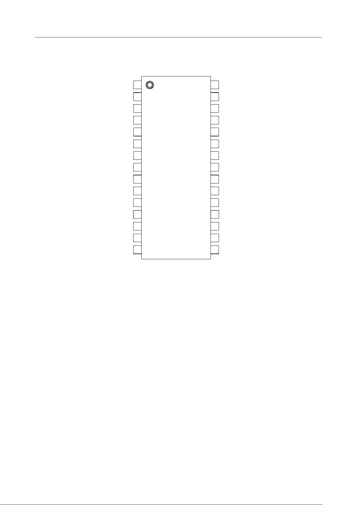
MSM9802/03/05-xxx¡ Semiconductor
V
DD
OSC1
OSC2
NC
NC
OSC3/TEST
NC
CPU/STD
NC
ST
NC
I2
30
29
28
27
26
25
24
23
22
21
20
16
AOUT
V
GND
NC
NC
NAR
NC
XT/CR
NC
RESET
NC
I3
1
2
3
4
5
6
7
8
9
10
11
12 19NC NC
13 18I0 I5
14 17I1 I4
15
REF
NC: No connection
30-Pin Plastic SSOP
Note: Applicable to MSM9802-xxxGS-AK, MSM9803-xxxGS-AK, and MSM9805-xxxGS-AK.
23/51
Page 24
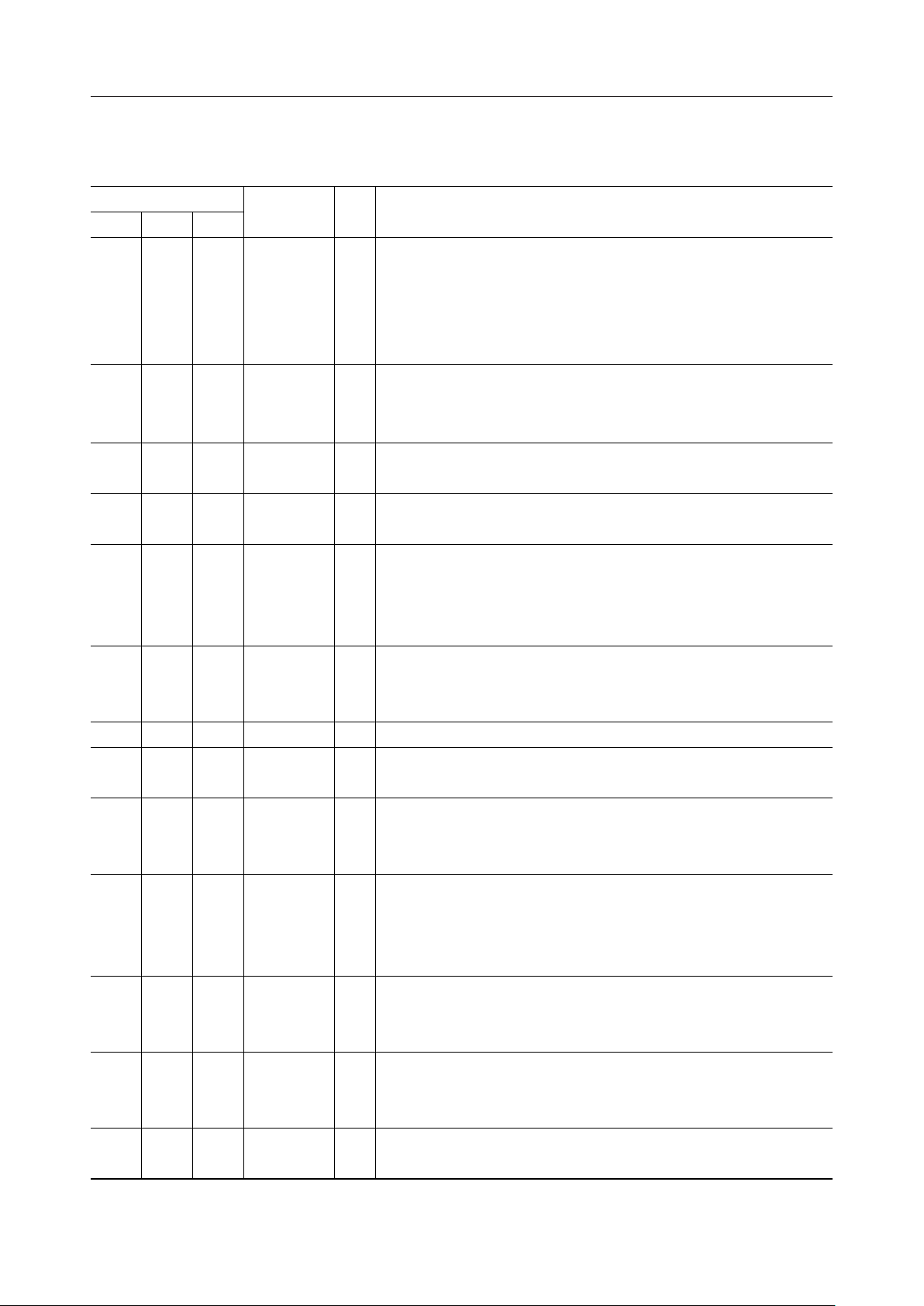
PIN DESCRIPTIONS
MSM9802/03/05-xxx¡ Semiconductor
Pin
DIP SOP SSOP
41721
62025
51823
14 7 8
82329
92430
72228
10 1 1
11 2 2
12 3 3
13 5 6
15810
16-18
10-15 13-18
1-3
Symbol Type Description
The IC enters the standby state if this pin is set to "L" level. At this time,
oscillation stops and AOUT drives a current of 0 mA and becomes GND
RESET I
level, then the IC returns to the initial state.
Apply a "L" pulse upon power-on.
This pin has an internal pull-up resistor.
Signal output pin that indicates whether the 6-bit LATCH (see Block
NAR O
Diagram) is idle. NAR at "H" level indicates that the LATCH is empty
and ST input is enabled.
XT/RC switching pin. Set to "H" level if ceramic oscillation is used.
XT/CR I
Set to "L" level if RC oscillation is used.
Microcontroller interface/stand-alone mode switching pin. Set to "H"
CPU/STD I
level if the MSM9802/03/05 is used in microcontroller interface mode.
Volume setting pin. If this pin is set to GND level, the maximum
V
REF
I
forced in. An approx. 10 kW pull-down resistor is internally connected
current is forced in, and if set to V
level, the minimum current is
DD
to this pin during operation.
Voice output pin.
AOUT O
The voice signals are output as current changes. In standby state, this
pin drives a current of 0 mA and becomes GND level.
GND —
Ground pin.
Power supply pin. Insert a bypass capacitor of 0.1 mF or more between
V
DD
—
this pin and the GND pin.
Ceramic oscillator connection pin when ceramic oscillation is selected.
OSC1 I
RC connection pin when RC oscillation is selected.
Input from this pin if external clock is used.
Ceramic oscillator connection pin when ceramic oscillation is selected.
RC connection pin when RC oscillation is selected.
OSC2 O
Leave this pin open if external clock is used.
Outputs "L" level in standby state.
Leave this pin open when ceramic oscillation is used.
OSC3/TEST O
RC connection pin when RC oscillation is selected.
Outputs "H" level in standby state when RC oscillation is selected.
Voice synthesis starts at fall of ST, and addresses I0 to I5 are fetched
ST I
at rise of ST. Input ST when NAR, the status signal, is at "H" level.
This pin has internal pull-up resistor.
Phrase input pins corresponding to playback sound.
I0 - I5 I
24/51
Page 25
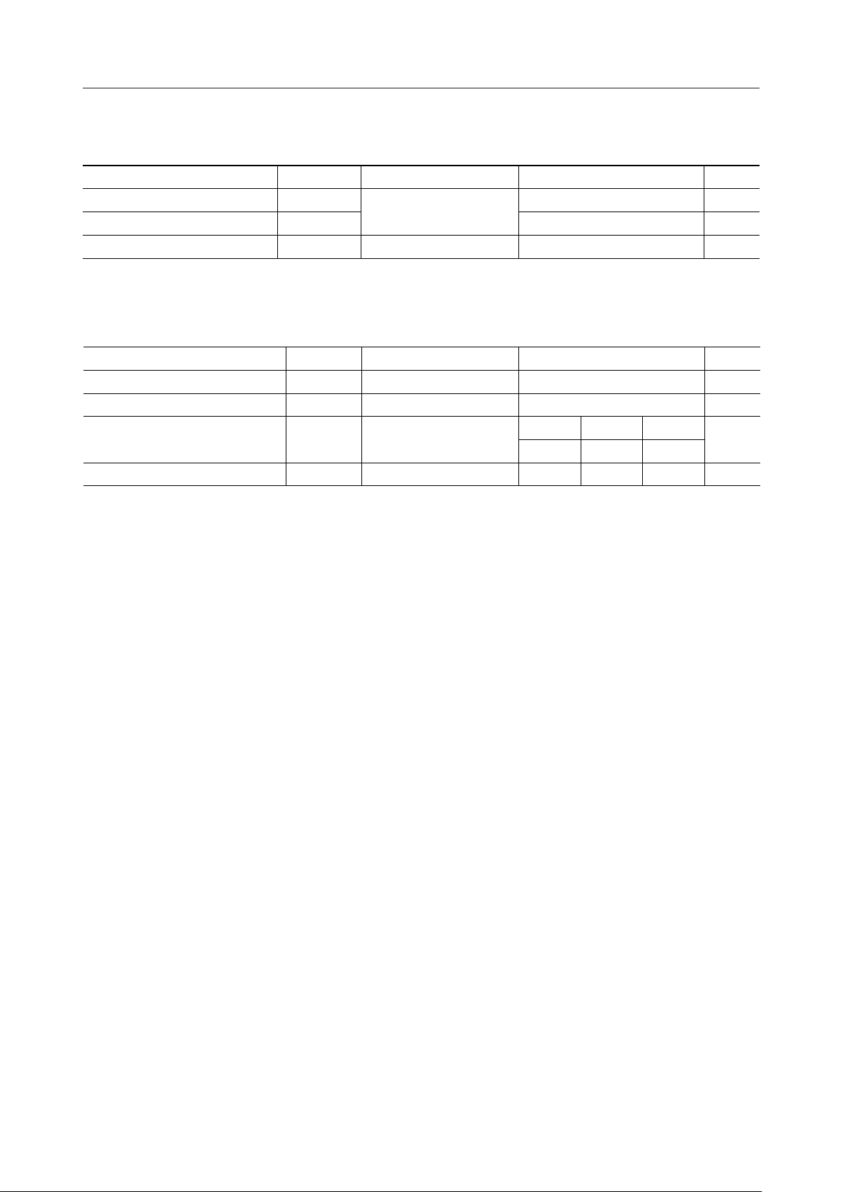
ABSOLUTE MAXIMUM RATINGS
Parameter Symbol Condition Rating Unit
Power Supply Voltage
Input Voltage
Storage Temperature
T
V
DD
V
STG
IN
Ta=25°C
RECOMMENDED OPERATING CONDITIONS
Parameter Symbol Condition Range Unit
Power Supply Voltage V
Operating Temperature —
Original Oscillation Frequency 1
T
f
OSC1
OSC2
DD
op
— 2.0 to 5.5 V
MSM9802/03/05-xxx¡ Semiconductor
–0.3 to +7.0 V
–0.3 to VDD+0.3 V
–55 to +150 °C—
–40 to +85 °C
Min. Max.
Typ.
4.0963.5 4.5
256200 300Original Oscillation Frequency 2 f
(GND=0V)
(GND=0 V)
MHzWhen crystal is selected
kHzWhen RC is selected (*1)
*1 The accuracy of the oscillation frequency when RC oscillation is selected depends largely on
the accuracy of the external R and C.
25/51
Page 26
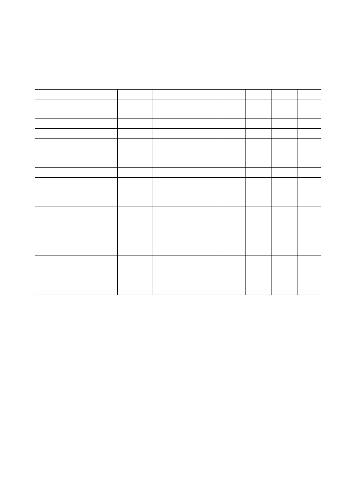
ELECTRICAL CHARACTERISTICS
DC Characteristics
(V
=5.0 V, GND=0 V, Ta=–40 to +85°C, unless otherwise specified)
DD
Parameter Symbol Condition Unit
"H" Input Voltage V
"L" Input Voltage —
*1
*2
*3
Standby Current I
V
Pin Pull-down Resistance
REF
IH
V
IL
V
OH
V
OL
IH1
Applies to OSC1 pin only.
IH2
IL1
IL2
DD1
AOUT bias voltage=0V
At maximum output current
DD2
V
AOUT bias voltage=0V
DS
At maximum output current,
AOUT
V
AOUT bias voltage=0V
R
VREF
MSM9802/03/05-xxx¡ Semiconductor
Min. Max.
——V
4.2 —
— 0.8
4.6 —
DD
V
IH=VDD
V
REF=VDD
REF
REF
,
=GND,
=GND,
Typ.
—V
—V"H" Output Voltage IOH=–1 mA
—— 0.4
——10"H" Input Current 1 I
——15"H" Input Current 2 I
—–10 —"L" Input Current 1 I
–90–200 –30"L" Input Current 2 I
0.4—1Dynamic Supply Current 1 I
——16Dynamic Supply Current 2 I
——10
V"L" Output Voltage IOL=2 mA
µAVIH=V
µA
µAVIL=GND
µAInternal pull-up resistor
mA
mA
µATa=–40 to +70°C
——50µATa=70 to 85°C
9.5615AOUT Output Current I
10713
mA
kW—
*1 Applicable to RESET, ST
*2 Dynamic supply current (excluding DAC output current)
*3 Dynamic supply current at maximum output current
26/51
Page 27
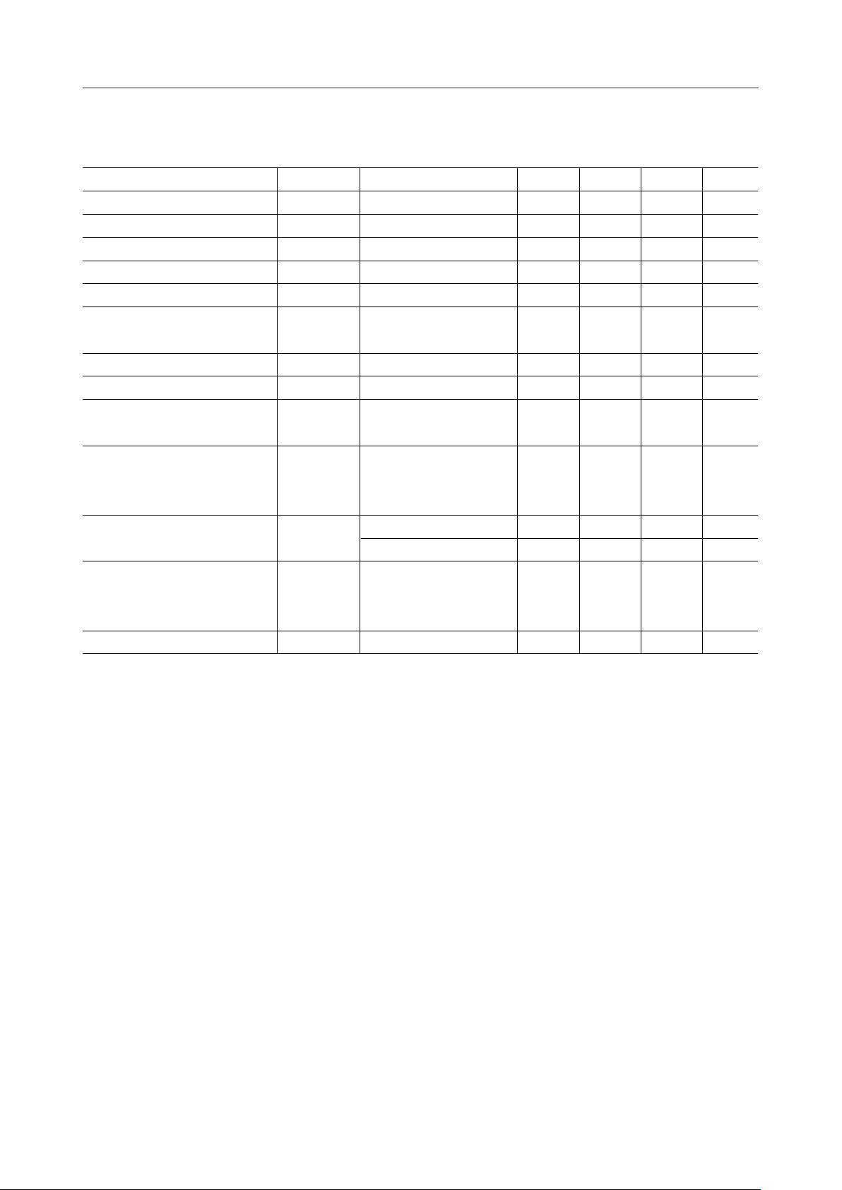
DC Characteristics
(V
=3.1 V, GND=0 V, Ta=–40 to +85°C, unless otherwise specified)
DD
Parameter Symbol Condition Unit
"H" Input Voltage V
"L" Input Voltage —
*1
*2
*3
Standby Current I
V
Pin Pull-down Resistance
REF
IH
V
IL
V
OH
V
OL
IH1
Applies to OSC1 pin only.
IH2
IL1
IL2
V
DD1
AOUT bias voltage=0V
At maximum output current
DD2
V
AOUT bias voltage=0V
DS
At maximum output current,
AOUT
V
AOUT bias voltage=0V
R
VREF
MSM9802/03/05-xxx¡ Semiconductor
Min. Max.
——V
2.7 —
— 0.5
2.6 —
DD
V
IH=VDD
REF=VDD
REF
REF
,
=GND,
=GND,
Typ.
—V
—V"H" Output Voltage IOH=–1 mA
—— 0.4
——10"H" Input Current 1 I
——15"H" Input Current 2 I
—–10 —"L" Input Current 1 I
–30–100 –10"L" Input Current 2 I
0.15— 0.5Dynamic Supply Current 1 I
—— 5.5Dynamic Supply Current 2 I
——5
V"L" Output Voltage IOL=2 mA
µAVIH=V
µA
µAVIL=GND
µAInternal pull-up resistor
mA
mA
µATa=–40 to +70°C
——20µATa=70 to 85°C
3.21.4 5AOUT Output Current I
10713
mA
kW—
*1 Applicable to RESET, ST
*2 Dynamic supply current (excluding DAC output current)
*3 Dynamic supply current at maximum output current
27/51
Page 28
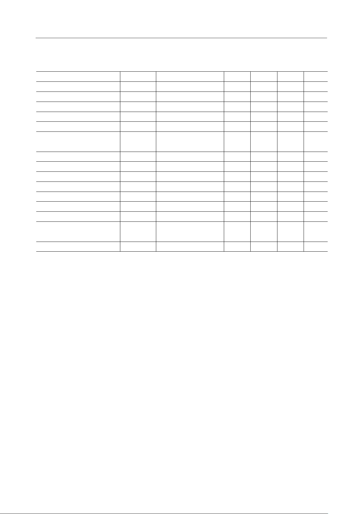
AC Characteristics
Parameter Symbol Condition Unit
Master Clock Duty Cycle f
RESET Input Pulse Width —
RESET Input Time After Power-on
Standby Transition Time
(at end of voice output)
duty
t
w(RST)
t
D(RST)
STP
t
(ST)
Upon entering the stop code
SS
DW
WD
SNS
NAA
NAB
NAC
, t
DAR
DAF
t
STB
BLN
MSM9802/03/05-xxx¡ Semiconductor
(V
=5.0 V, GND=0 V, Ta=–40 to +85°C)
DD
Min. Max.
—50%
40 60
10 —
—
0—
1
40
(note)
=8 kHz
SAM
SAM
SAM
SAM
=8 kHz
=8 kHz
=8 kHz
(note)
(note)
(note)
(note)
(note)
SAM
=8 kHz
(note)
Typ.
—µs
—µs
——t
—0.35 2000
——t
—1—Data Setup Time t
—1—Data Hold Time t
——10NAR Output Time (1) t
375350 400NAR Output Time (2) t
440315 500NAR Output Time (3) t
375350 500NAR Output Time (4) t
6460 68D/A Converter Change Time t
250200 300
375350 500Silence Time Between Phrases t
µsST Signal Setup Time At power-on
µsST Input Pulse Width —
µsST-ST Pulse Interval
µs—
µs—
µsf
µsf
µsf
µsf
ms—
ms—
µsf
(Note) Proportional to master the periods of oscillation frequencies f
The rated values show values when the standard master oscillation frequency is used.
OSC1
and f
OSC2
.
28/51
Page 29
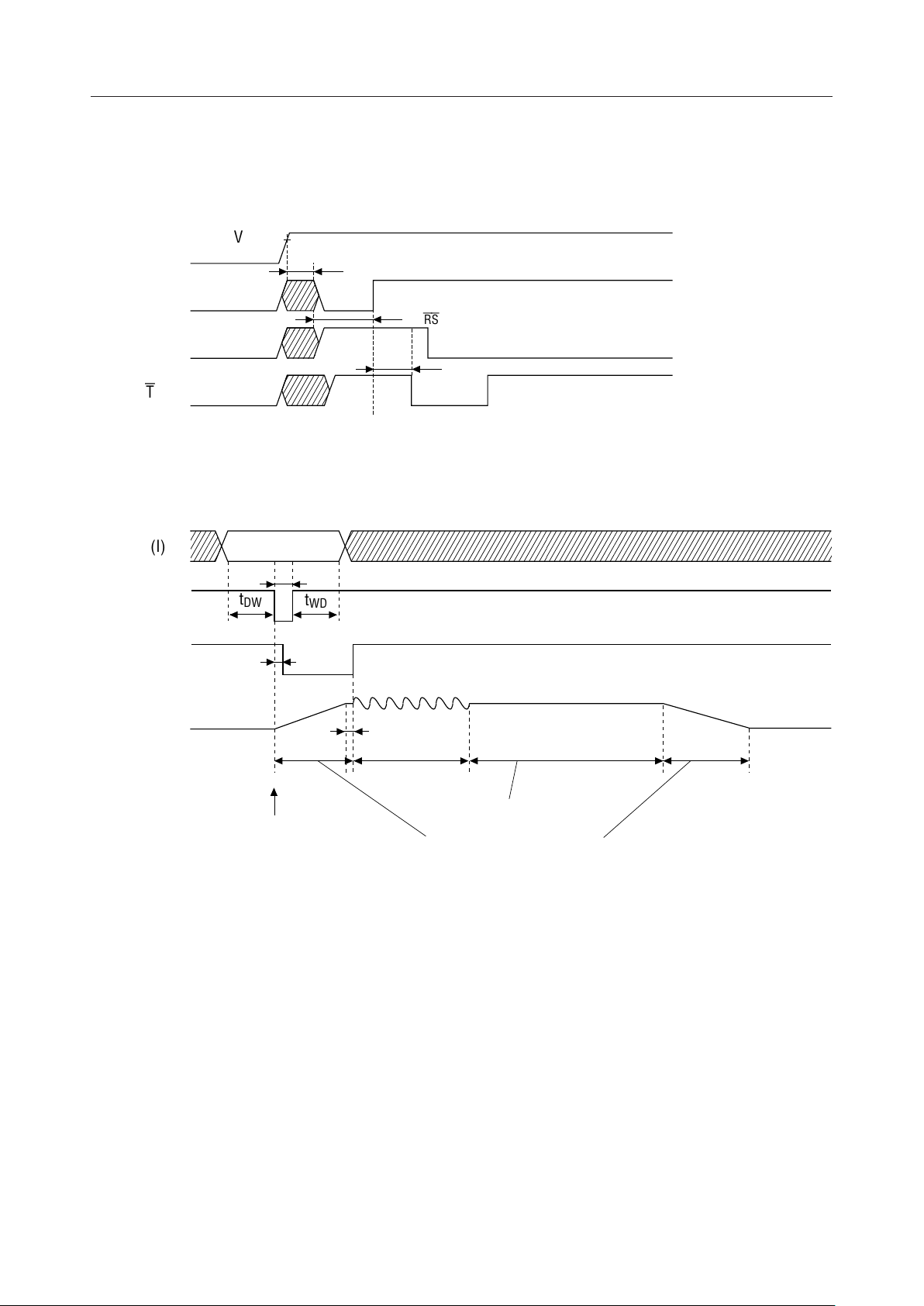
TIMING DIAGRAMS
g
AC Characteristics at Power-On
MSM9802/03/05-xxx¡ Semiconductor
V
DD
VDDMin
t
D(RST)
RESET (I)
t
W(RST)
NAR (O)
t
STP
ST (O)
AC Characteristics in Standby Status and when the IC is Activated
I5-I0 (I)
t
(ST)
ST (
I
NAR (O)
t
)
DW
t
t
WD
SNS
AOUT (O)
t
DAR
Oscillation start
t
NAA
Voice playback
Standby transition time
D/A converter chan
t
STB
e time
t
DAF
29/51
Page 30
30/51
MSM9802/03/05-xxx¡ Semiconductor
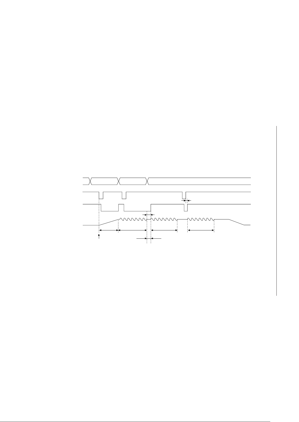
Playback Timing
AOUT (O)
t
DAR
NAR (O)
ST (
I
)
I5-I0 (I)
1st phrase address 2nd phrase address 3rd phrase address
1st phrase
playback
2nd phrase
playback
3rd phrase
playback
t
NAC
Oscillation start
t
NAB
t
BLN
Page 31
MSM9802/03/05-xxx¡ Semiconductor
FUNCTIONAL DESCRIPTION
1. Playback Code Specification
The user can specify a maximum of 63 phrases. Table 1.1 shows the settings by the I5-I0 pins.
Table 1.1 User-specified Phrases
I5-I0
000000
000001
111111
Code Details
Stop code
User-specified phrase
(63 Phrases)
2. Address Data
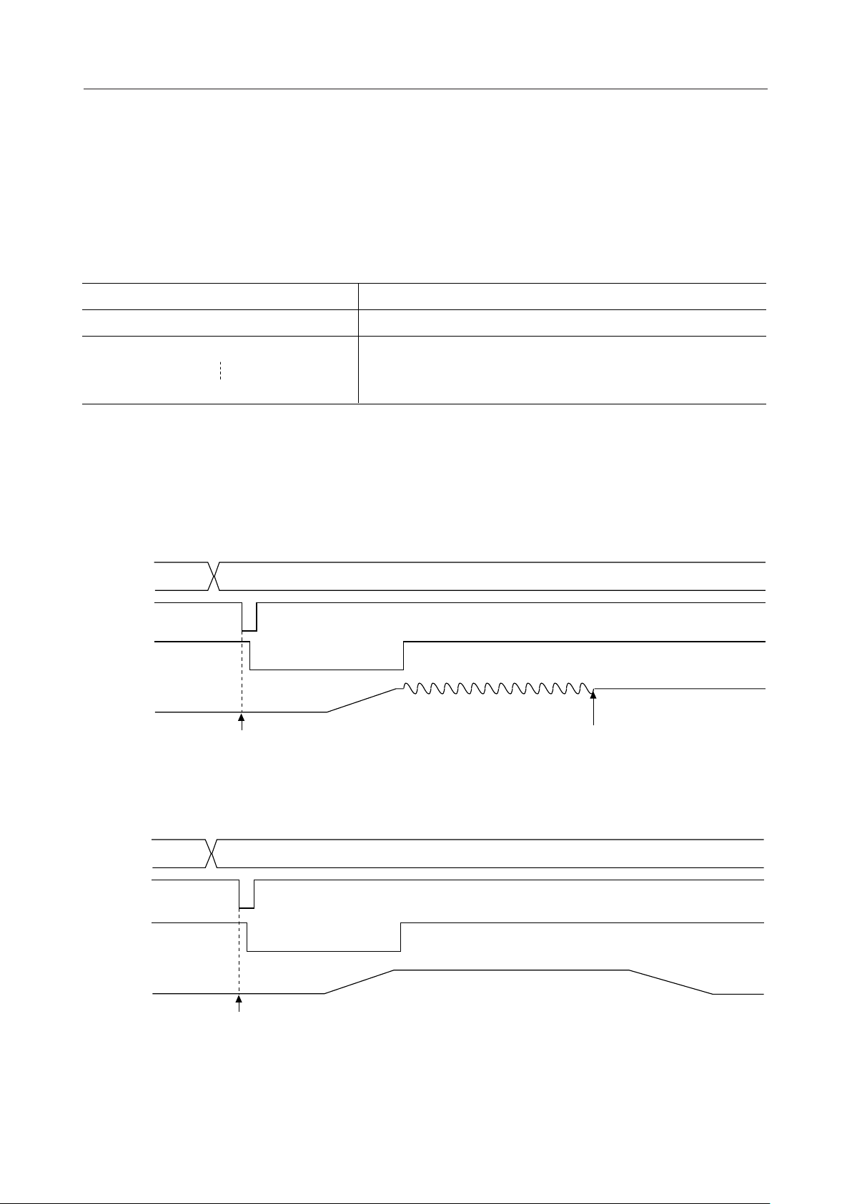
If a phrase is input at I5-I0 pins by address data, and if a ST pulse is then applied, voice playback
starts. Figure 2.1 shows voice start timing. Figure 2.2 shows timing when an address other than
a phrase is input.
I5-I0 (I)
ST (
I
NAR (O)
AOUT (O)
)
User phrase
I5-I0 (I)
ST (
I
NAR (O)
AOUT (O)
Oscillation start Voice end
Figure 2.1 Voice Start Timing
Address other than user phrase
)
Oscillation start
Figure 2.2 Timing when Address Other than a Phrase
is Input in Stand-by Mode
31/51
Page 32
MSM9802/03/05-xxx¡ Semiconductor
p
3. Stop Code
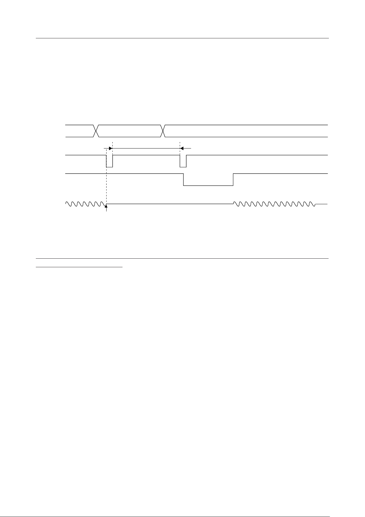
If I5-I0 are set to "000000" during voice playback, and a ST signal is input, playback stops
regardless of whether NAR is at "H" or "L" level, then AOUT becomes 1/2 I
AOUT
. Stop code
becomes valid at the falling edge of ST.
Figure 3.1 shows stop code input timing.
I5-I0 (I)
ST (
I
NAR (O)
AOUT (O)
t
SS
)
Voice sto
User phrase"000000"
Figure 3.1 Stop Code Input Timing
The stop code does not initialize internal units but only stops playback. To initialize an internal
register, use the RESET pin.
32/51
Page 33
MSM9802/03/05-xxx¡ Semiconductor
4. Generating Pseudo-BUSY Signal through NAR Pin
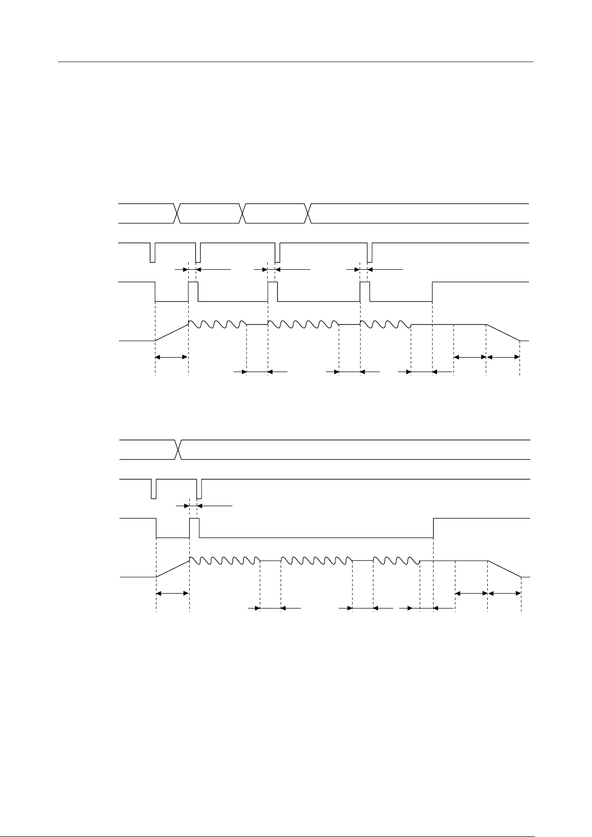
If the application in use requires a BUSY signal when this IC is used in microcontroller interface
mode, a pseudo-BUSY signal can be generated through the NAR pin by controlling signal timing,
as shown below.
4.1 When edit ROM is not used
01 (Phrase 1) 02 (Phrase 2) 03 (Phrase 3) 04 (Silence phrase of 32 ms or more)
I5-I0
ST
30ms or more 30ms or more 30ms or more
NAR
(Pseudo-BUSY)
AOUT
t
DAR
Phrase 1
Phrase 2 Phrase 3
t
NAB
t
NAB
Silence
phrase
t
NAB
t
STB
t
DAF
4.2 When edit ROM is used
I5-I0
ST
NAR
(Pseudo-BUSY)
AOUT
01
(Phrases 1+2+3)
t
DAR
02 (Silence phrase of 32 ms or more)
30ms or more
Phrase 1
t
BLN
Phrase 2
Phrase
t
BLN
Silence
3
phrase
t
NAB
t
STB
t
DAF
33/51
Page 34
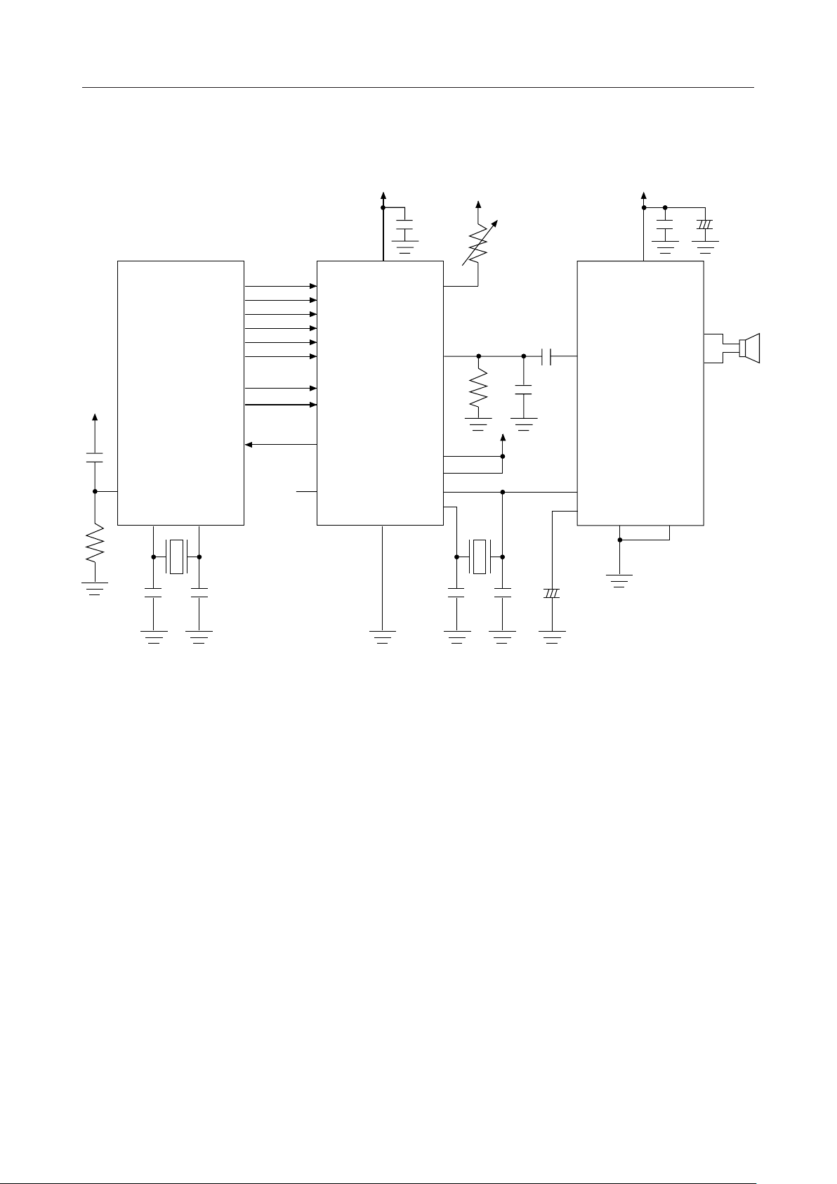
APPLICATION CIRCUIT
MSM9802/03/05-xxx¡ Semiconductor
+
–
RESET
P1.5
P1.4
P1.3
P1.2
P1.1
P1.0 I0
P2.2
P2.1
MSM83C154 (MCU)
P3.0 NAR
XTAL2XTAL1
Application Circuit in Microcontroller Interface
I5
I4
I3
I2
I1
ST
RESET
OSC3
V
DD
V
REF
AOUT
MSM9802/03/05
CPU/STD
XT/CR
OSC2
OSC1
GND
V
CC
SP
A
IN
STBY
VR
GND
+
–
SP
MSC1157 (Speaker AMP)
SEL
34/51
Page 35
MSM9802/03/05-xxx¡ Semiconductor
(3) Common
1. Sampling Frequency
As shown in Table 1.1, 7 sampling frequencies are available.
A sampling frequency can be selected and assigned to each phrase in ROM data.
Table 1.1 Sampling Frequency
Sampling Frequency
At standard
oscillation frequency
4.0 kHz f
5.3 kHz f
6.4 kHz f
8.0 kHz f
10.6 kHz f
12.8 kHz f
16.0 kHz f
Ceramic Oscillation
Frequency diving ratio
XT/CR="H"
/1024 f
OSC1
/768 f
OSC1
/640 f
OSC1
/512 f
OSC1
/384 Unavailable
OSC1
/320 Unavailable
OSC1
/256 Unavailable
OSC1
XT/CR="L"
CR Oscillation
/64
OSC2
/48
OSC2
40
OSC2/
/32
OSC2
Note: When RC oscillation is selected, 10.6 kHz, 12.8 kHz, and 16 kHz cannot be selected.
2. Recording/Playback Time
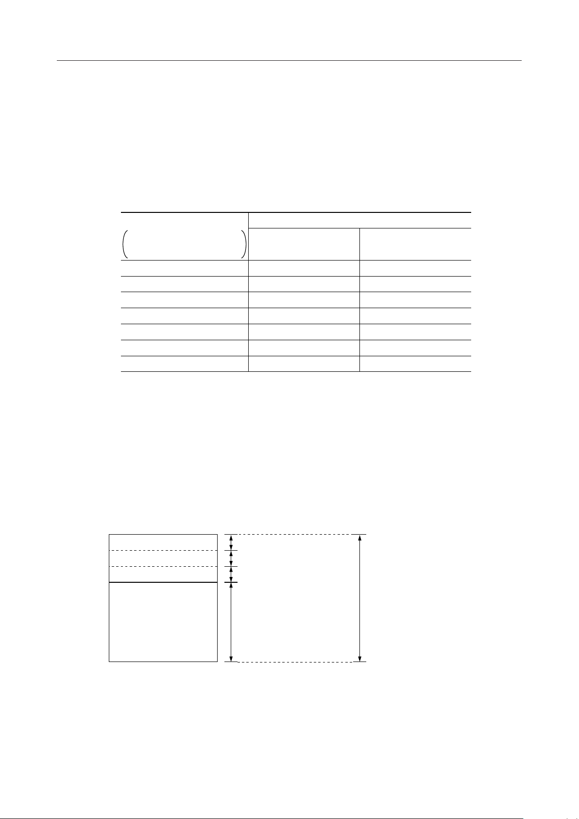
Figure 2.1 below shows memory allocation of the on-chip Mask ROM. About 11 Kbits of data area
is allocated for the Phrase Control Table, Phrase Data Control and Test Data.
Therefore, actual data area for storing sound data equals the total Mask ROM capacity minus 11
Kbits.
Phrase Control Table Area
Pharase Data Control Area
Test Data Area
User's Area
Figure 2.1 Memory Allocation of On-chip Mask ROM
4K bit
4K bit
3K bit
501K bit (MSM9802)
1013K bit (MSM9803)
2037K bit (MSM9805)
On-chip Mask ROM Capacity
512K bit (MSM9802)
1M bit (MSM9803)
2M bit (MSM9805)
35/51
Page 36
MSM9802/03/05-xxx¡ Semiconductor
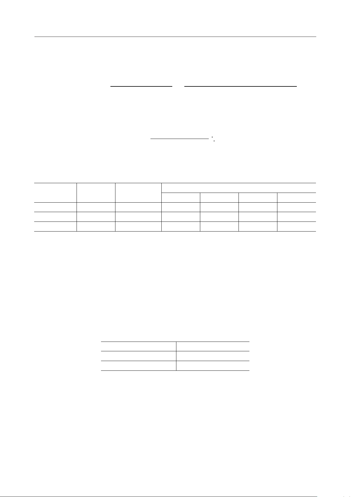
The playback time is obtained by dividing the memory capacity by the bit rate.
The playback time for 8-bit PCM algorithm is obrained by using the following equation.
Playback time [sec] = =
Memory capacity [bit]
Bit rate [bps]
Memory capacity [bit]
Sampling frequency [Hz] ¥ 8 [bit]
For example, if all phrases are stored in the MSM9802 at 8 kHz sampling frequency, the
maximum playback time is as follows.
Playback time =
(512–11) ¥ 1024 [bit]
8000 [Hz] ¥ 8 [bit]
=
8.0 [sec]
Table 2.1 Maximum playback time
Model
MSM9802
MSM9803
MSM9805
ROM capacity
512K bit
1M bit
2M bit
User's area
501K bit
1013K bit
2037K bit
f
SAM
=4.0kHz
16.0
32.4
65.1
Maximum playback time (sec)
f
f
SAM
=6.4kHz
10.0
20.2
40.7
SAM
=8.0kHz
8.0
16.2
32.5
f
SAM
=16.0kHz
4.0
8.1
16.2
3. Playback Method
This IC provides two kinds of playback methods, non-linear PCM algorithm and straight PCM
algorithm. When the 8-bit non-linear PCM algorithm is selected, sound quality can be improved
because a resolution equivalent to 10-bit straight PCM is available around the waveform center.
You can select either non-linear PCM algorithm or straight PCM algorithm for each phrase. Table
3.1 shows the relationship between playback methods and applicable sounds. It is recommended to evaluate the sound quality before actual use.
Table 3.1 Relationship between playback methods and applicable sounds
Playback method Applicable sound
8-bit non-linear PCM algorithm Human voice
8-bit straight PCM algorithm BEEP tone, sound effects
36/51
Page 37
MSM9802/03/05-xxx¡ Semiconductor
4. Phrase Control Table
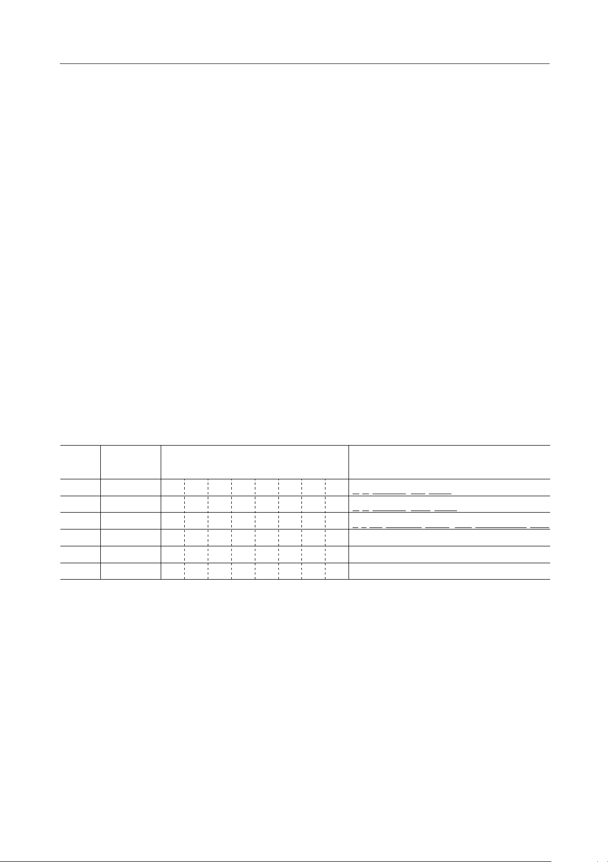
Because the LSI contains the Phrase Control Table, it is possible to play back multiple phrases in
succession by a single easy control operation like controlling a single regular phrase playback.
Up to 8 combined phrases including a silence can be registered in a single address in the Phrase
Control Table.
Further, you can use the maximum memory space for data storage because it is not required to
have the same phrase data.
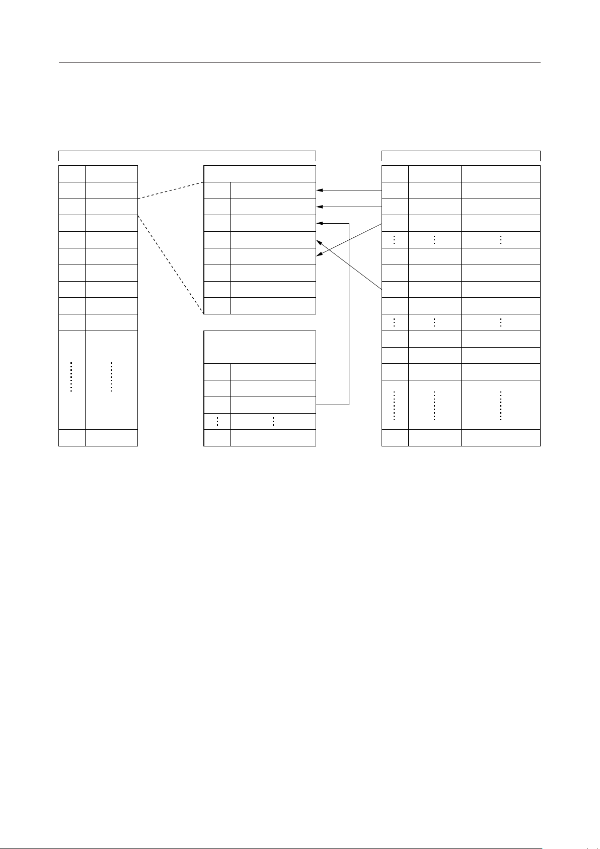
To show an example, let's assume that your application needs to speak two similar sentences, "It
is fine today" and "It is rainy today." The two sentences have the common words "it", "is" and
"today". What you have to do is to prepare these common sound data, not in sentences but in
words, and to store each combined phrase data in Phrase Control Table as shown in Table 4.1 and
Figure 4.1
Multiple phrases can be played continuously merely by specifying a desired phrase using an X
address. For an example from Table 4.1, when address "01" is specified, "It is fine today" is played,
and when address"02" is specified, "It is rainy" is played.
Phrase Control Table, a silence can be inserted without using the User's Area.
Minimum time for silence 32 ms
Maximum time for silence 2016 ms
Time unit for setting up silence 32 ms
No.
X-Address
(HEX)
101
202
303
· · ·
62 3E
63 3F
· · ·
Table 4.1 Matrix of the Phrase Control Table
Y-Address
(Up to 8 phrases)
[10]
Silence
[02][01] [03]
Silence
[02][01] [03]
[12]
[21][10][02][01] [11] [12] [22] [03]
It is (silence) fine today.
It is (silence) rainy today.
It is fine becoming cloudy, rainy in some areas today.
Sound Data
· · ·
37/51
Page 38
MSM9802/03/05-xxx¡ Semiconductor
Figure 4.1 Phrase Combination Matrix for Phrase Control Table
No. X-Address
101
202
303
404
505
606
707
808
909
Phrase Control Table Area
Phrase Addigned
1 [01]
2 [02]
3 Silence (64ms)
4 [12]
5 [03]
6—
7—
8—
Silence time setting
0 Silence time
1 32 ms
2 64 ms
(32ms ¥ n)
it
is
rainy
today
Phrase Data Registration Area
No. Y-Address Phrase
101
202
303
16 10
17 11
18 12
19 13
32 20
33 21
34 22
it
is
today
fine
cloudy
rainy
snowy
ocasionally
becoming
in some areas
63 3F
63 2016 ms
63 3F —
38/51
Page 39
MSM9802/03/05-xxx¡ Semiconductor
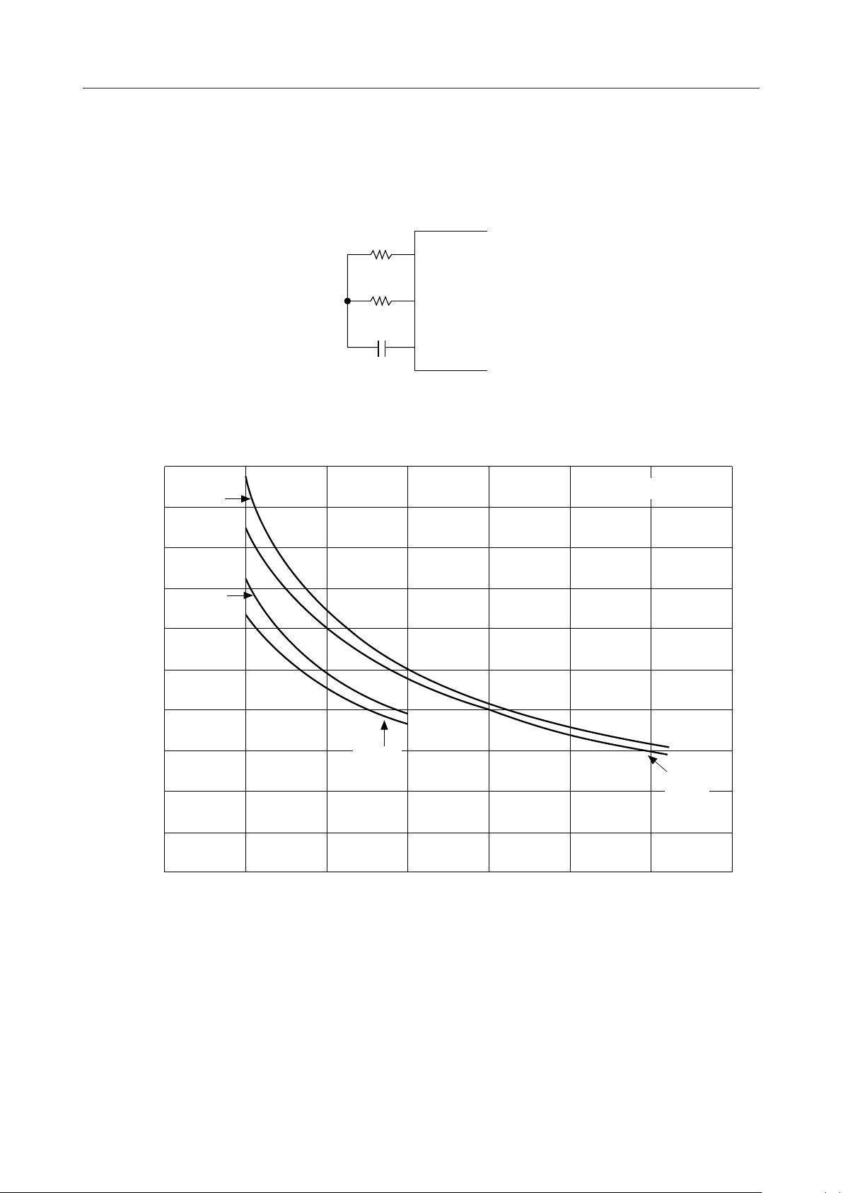
5. RC Oscillation
Figure 5.1 shows an external circuit using RC oscillation. Figure 5.2 shows the RC oscillation
frequency characteristics.
R1
OSC1
R2
OSC2
C
OSC3
Figure 5.1 RC Oscillation
500
450
VDD=5 V
C=30 pF
R1=100 kW
400
350
(kHz)
OSC
300
VDD=5 V
C=47 pF
250
200
150
Oscillaiton Frequency f
100
50
0
VDD=3 V
C=47 pF
VDD=3 V
C=30 pF
10 20 30 40 50 60 70
Load Resistance R2 (kW)
Figure 5.2 RC Oscillation Frequency Characteristics
39/51
Page 40
5.1 Determining RC constants
MSM9802/03/05-xxx¡ Semiconductor
The RC oscillation frequency characteristics are shown in Figure 5.2. If f
is set to 256 kHz, use
osc
the following values as a guide (see Figure 5.2) to set the C and R2 that fit the printed-circuit board
type used.
R1=100 kW, R2=30 kW, C=30 pF
When choosing RC oscillation, the RC oscillation frequency varies according to the fluctuation
of the external C and R2.
5.2 Fluctuation of RC oscillation frequencies
When choosing RC oscillation, the error of RC oscillation frequency due to process variations of
the IC is ±4% maximum, and the fluctuation of the RC oscillation frequency when using a
capacitor (C) of ±1% accuracy and a resistor (R2) of ± 2% accuracy is a maximum of ±7%
approximately.
6. Ceramic Oscillation
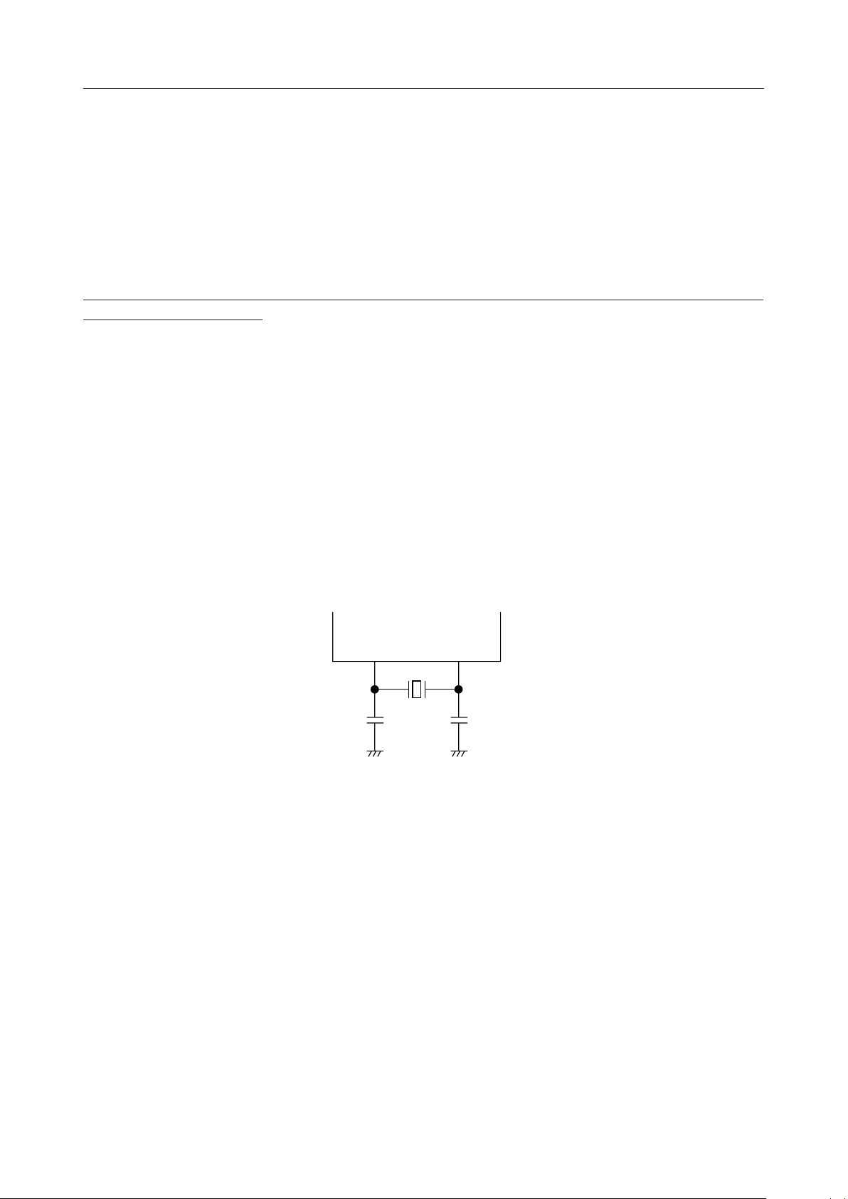
Figure 6.1 shows an external circuit using a ceramic oscillator.
OSC1 OSC2
C1 C2
Figure 6.1 Ceramic Oscillation Diagram
40/51
Page 41
MSM9802/03/05-xxx¡ Semiconductor
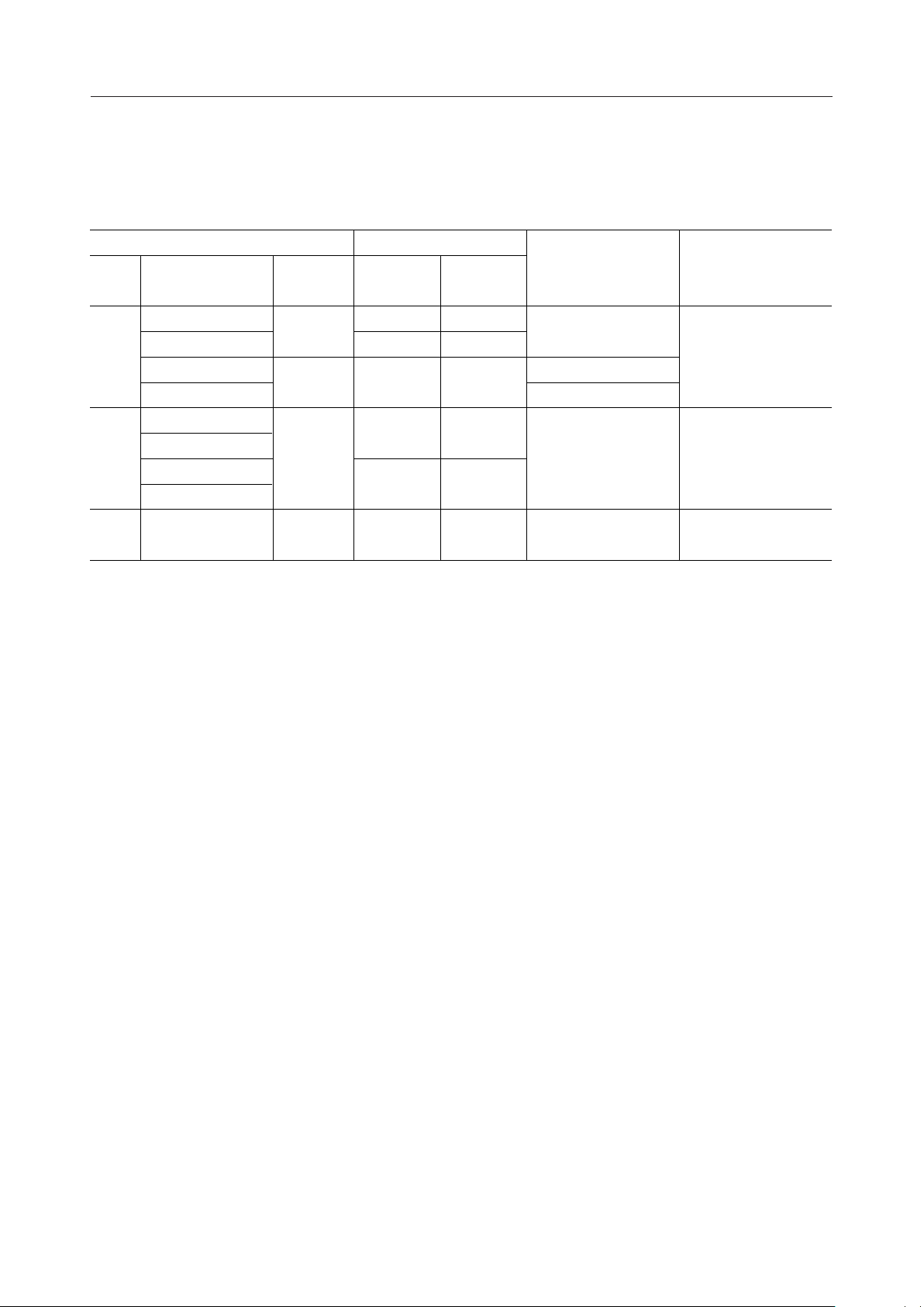
For example, the following table shows the optimum load capacitances, power supply voltage
ranges, and operating temperature ranges when ceramic oscillators made by Murata MFG Co.,
Ltd., Kyocera Co., Ltd. and TDK Co., Ltd. are used.
Maker
Murata MFG.KyoceraTDK
Ceramic oscillator
Type
CSA4.09MGU
CST4.09MGWU
CSTCC4.00MG 3.6 to 5.5
CSTCC4.00MGU
PBRC4.00A
KBR-4.0MSB
PBRC4.00B
KBR-4.0MKC
CCR4.00MC3 4.0 –40 to +852.4 to 5.5
Frequency
(MHz)
4.096
4.0
4.0 –20 to +803.1 to 5.5
Optimal load capacity
C1 (pF) C2 (pF)
30 30
Built in Built in
15 15
33 33
Built in Built in
Built in Built in
supply voltage range
(V)
3.0 to 5.5
2.7 to 5.5
Operating
temperature range
(°C)
–40 to +85
(Note) When a 4 MHz ceramic oscillator is used, the playback speed of MSM9802/03/05 is
slower by 2 percent than that of an analysis tool or a demonstration board.
41/51
Page 42
MSM9802/03/05-xxx¡ Semiconductor
[Hz]
7. Low-Pass Filter
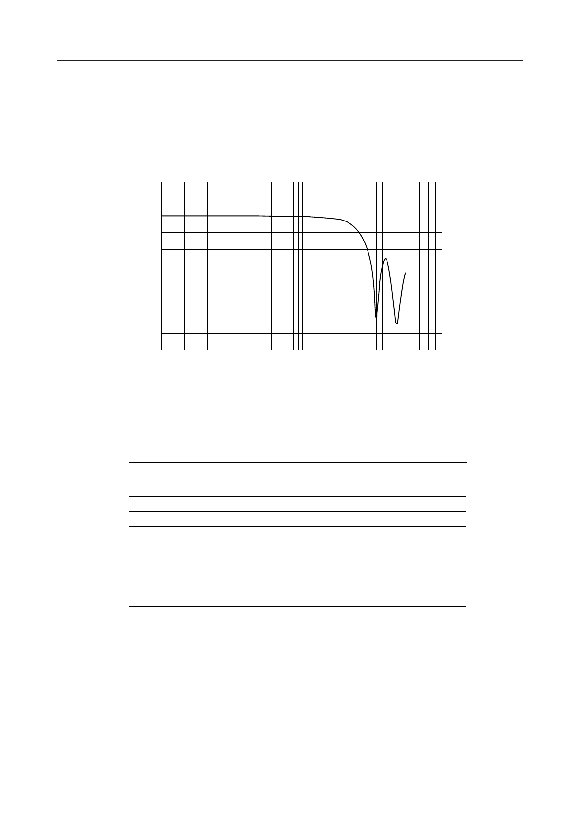
In this IC, all voice outputs are through the built-in low-pass filter (LPF). Figure 7.1 and Table
7.2 show the LPF frequency characteristics and LPF cutoff frequency respectively.
Only the voice output through LPF is enabled in this IC.
20
[dB]
10
0
–10
–20
–30
–40
–50
–60
–70
–80
10
100 1k 10k
Figure. 7.1 LPF Frequency Characteristics (f
Table 7.2 LPF Cutoff Frequency
Sampling Frequency (kHz) Cutoff Frequency (kHz)
(f
(f
4.0
5.3
6.4
8.0
10.6
12.8
16.0
SAM
)
CUT
1.2
1.6
2.0
2.5
3.2
4.0
5.0
SAM
)
=8 kHz)
42/51
Page 43
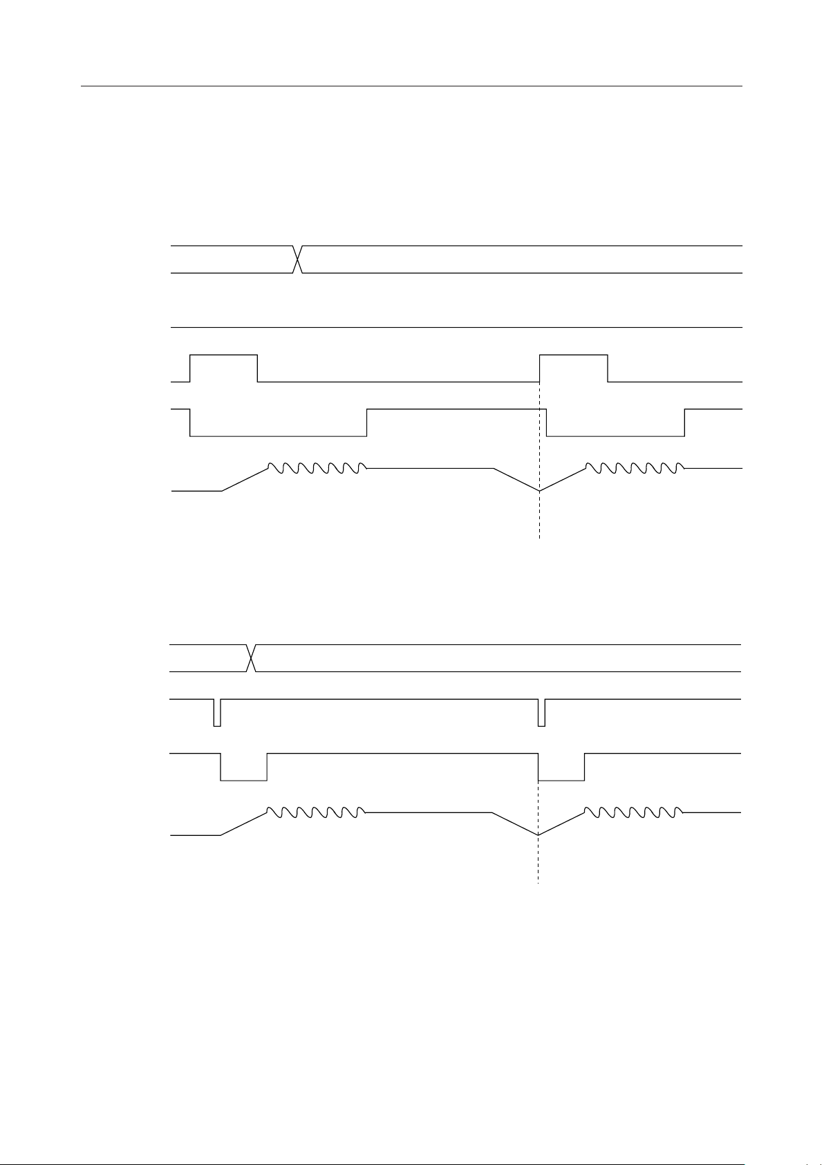
8. Standby Transition
MSM9802/03/05-xxx¡ Semiconductor
When playback of a phrase is finished, if playback of the next phrase does not start up within t
(0.25 sec. typ.), the IC enters standby status and the entire operation stops.
A2 - A0
SW2 - SW1 "L"
SW0
BUSY
AOUT
Figure 8.1 Timing for Voice Playback during D/A Converter Change Time
(Stand-alone Mode)
STB
I5 - I0
ST
NAR
AOUT
Figure 8.2 Timing for Voice Playback during D/A Converter Change Time
(Microcontroller Interface Mode)
If playback is attempted during D/A converter change time as shown in figures 8.1 and 8.2, the
IC exits from standby status and the output from the D/A converter begins going to the
1/2 I
level. When the output reaches 1/2 I
AOUT
, voice playback starts.
AOUT
43/51
Page 44
MSM9802/03/05-xxx¡ Semiconductor
(
)
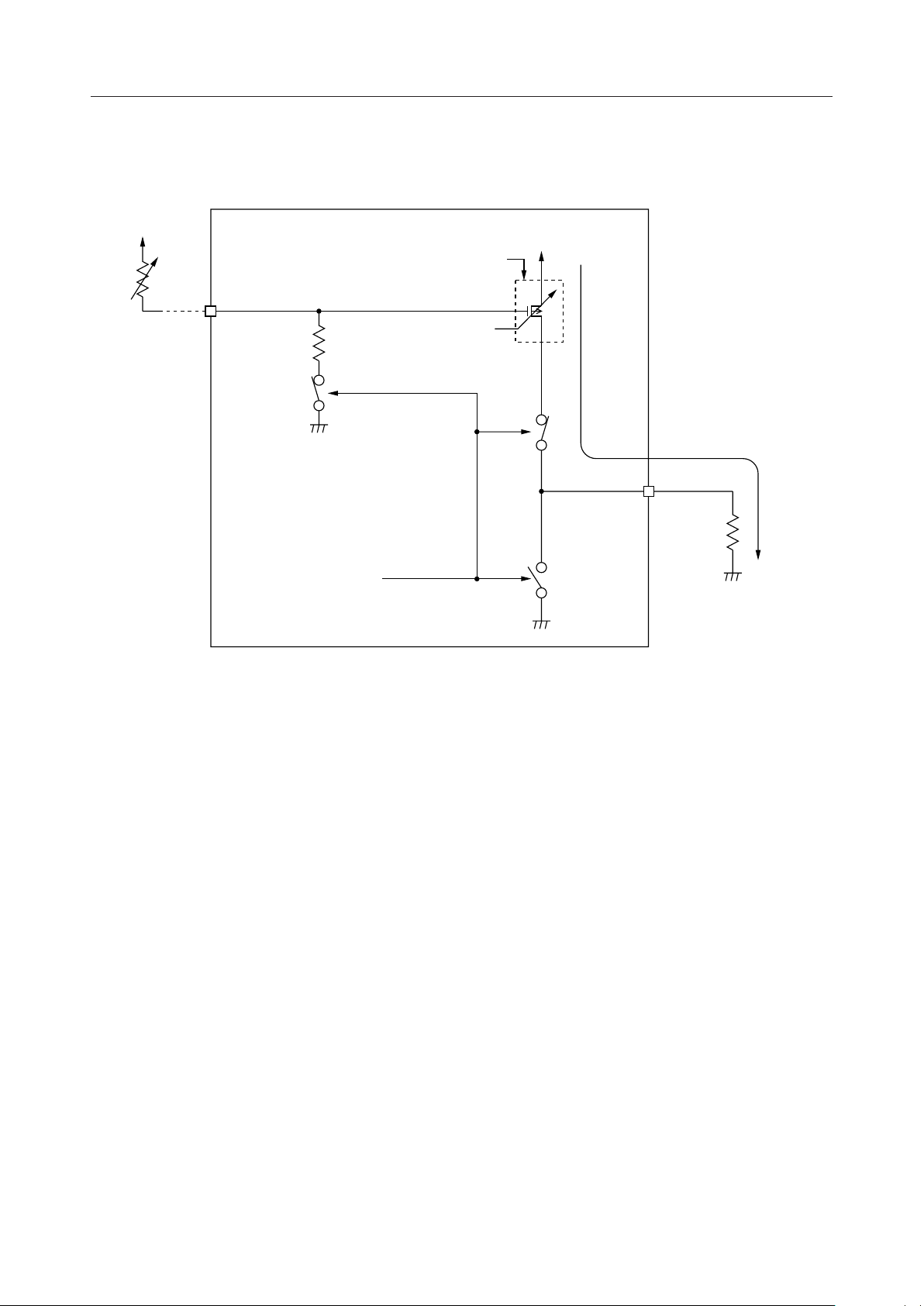
9. Voice Output Unit Equivalent Circuit (AOUT, F
Current-Sourcing Type
D/A Converter
V
REF
10kW
(TYP)
Standby Signal
PCM Value
REF
V
Pins)
DD
AOUT
I
AOUT
The above switch positions show those when the circuit is active.
Figure 9.1 Voice Output Unit Equivalent Circuit
44/51
Page 45
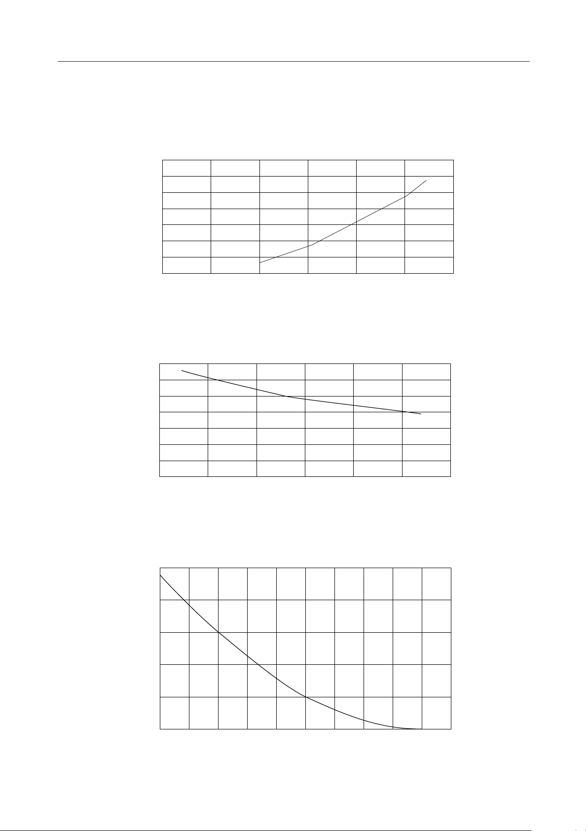
D/A CONVERTER OUTPUT CURRENT CHARACTERISTICS
]
]
MSM9802/03/05-xxx¡ Semiconductor
Power Supply Voltage vs. Output Current Characteristics (Ta=25°C, V
14
12
10
8
6
4
2
AOUT Output Current [mA]
0
0123456
Power Supply Voltage [V
Temperature vs. Output Current Characteristics (VDD=5V, V
14
12
10
8
6
4
2
AOUT Output Current [mA]
0
–50 –25 0 25 50 75 100
AOUT
AOUT
=0V)
=0V)
Ambient Temperature Ta [°C
V
Voltage vs. Output Current Characteristics (Ta=25°C, V
REF
10
8
6
4
2
AOUT Output Current [mA]
0
0.0 0.5 1.0 1.5 2.0 2.5 3.0 3.5 4.0 4.5 5.0
[V]
V
REF
DD
=5V, V
AOUT
=0V)
45/51
Page 46
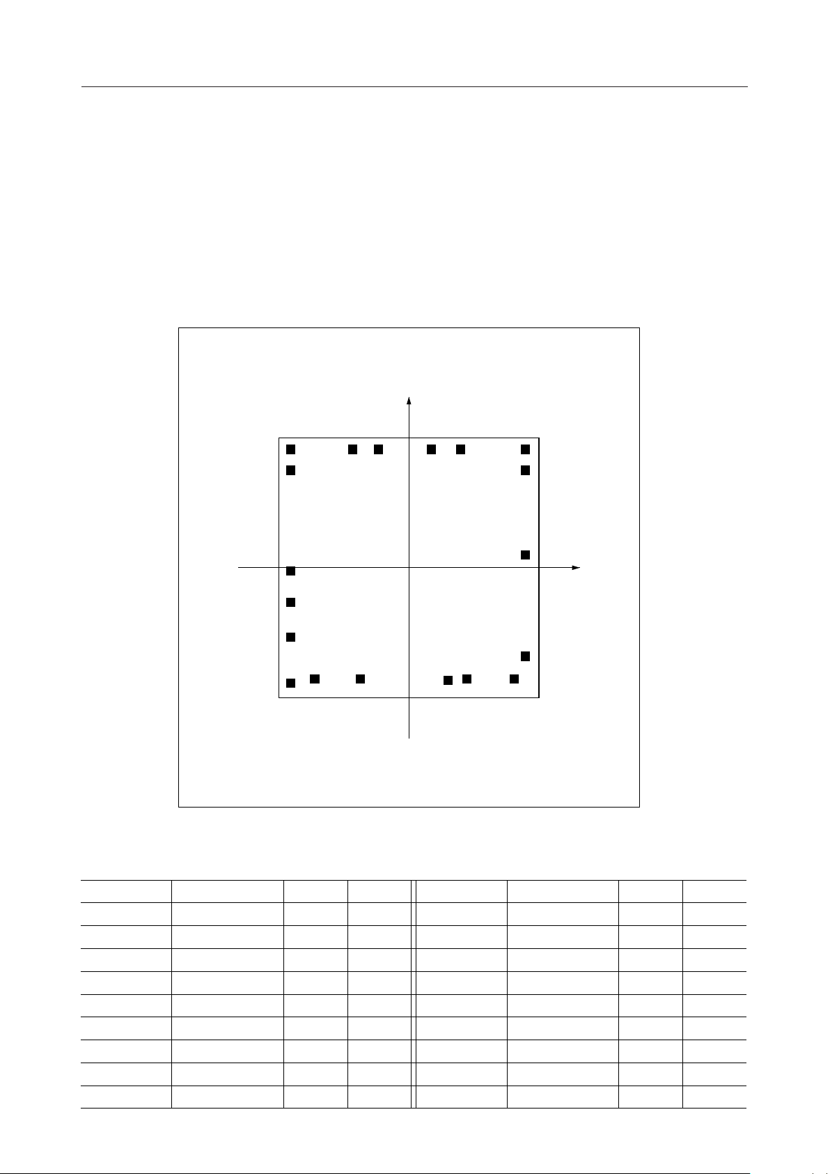
PAD CONFIGURATION
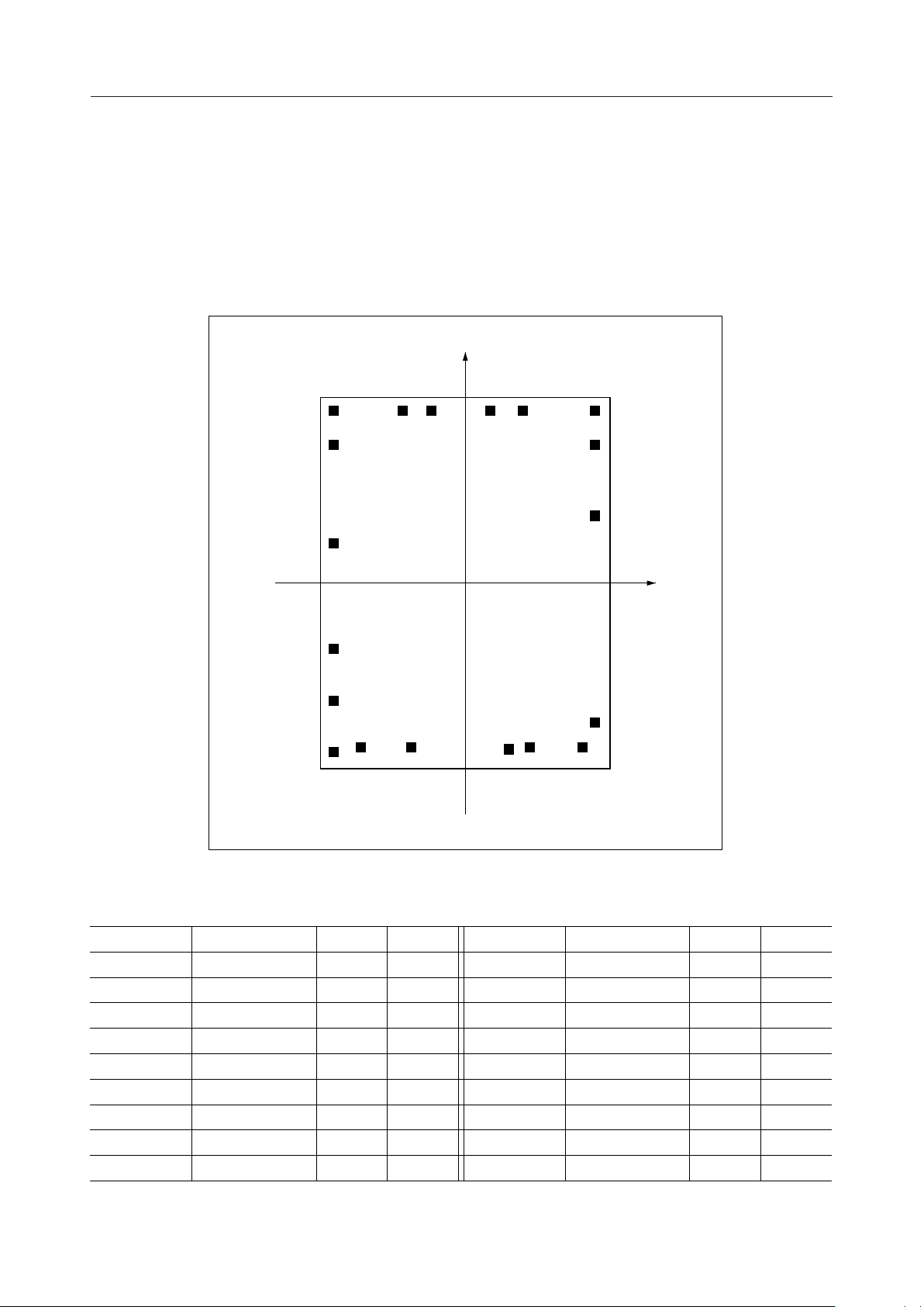
MSM9802
Pad Layout
Chip size : X=3.22mm Y=3.17mm
Chip thickness : 350µm ± 30µm
Pad size : 110µm ¥ 110µm
Substrate potential : GND
Y-axis
3 2 1 18 17 16
MSM9802/03/05-xxx¡ Semiconductor
154
(NC)
MSM9802
5
6
8 9 10 11 12
7
14
X-axis
13
Pad Coordinates
(Chip center is located at X=0 and Y=0)
(Unit: µm)
Pad No. Pad Name X-axis Y-axis Pad No. Pad Name X-axis Y-axis
1 I3/ (A0) –415 1385 10 V
2 I4/ (A1) –816 1385 11 OSC1 742 –1333
3 I5/ (A2) –1460 1385 12 OSC2 1349 –1333
4 RESET –1460 1049 13 OSC3 1460 –972
5 XT/CR –1458 –20 14 CPU/STD 1389 183
6 NAR –1460 –899 15 ST/(RND) 1389 1058
7 GND –1460 –1375 16 I0/(SW0) 1389 1385
8V
9 AOUT –585 –1333 18 I2/(SW2) 276 1385
REF
–1135 –1333 17 I1/(SW1) 719 1385
DD
462 –1347
Pad name in parentheses is for stand-alone mode.
46/51
Page 47
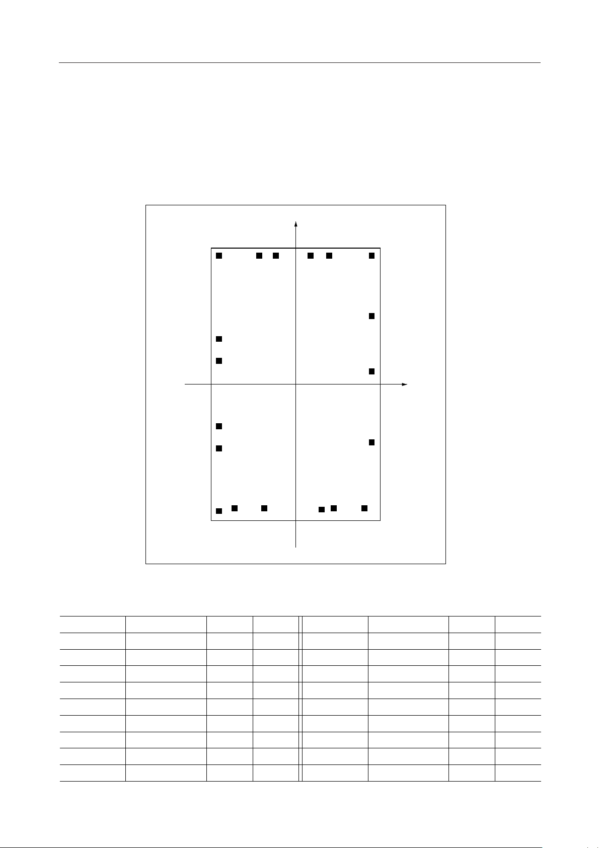
MSM9803
Pad Layout
Chip size : X=3.22mm Y=4.06mm
Chip thickness : 350µm ± 30µm
Pad size : 110µm ¥ 110µm
Substrate potential : GND
Y-axis
3 2 1 18 17 16
MSM9802/03/05-xxx¡ Semiconductor
154
14
X-axis
13
(NC)
5
6
7
MSM9803
8 9 10 11 12
Pad Coordinates
(Chip center is located at X=0 and Y=0)
(Unit: µm)
Pad No. Pad Name X-axis Y-axis Pad No. Pad Name X-axis Y-axis
1 I3/ (A0) –415 1829 10 V
2 I4/ (A1) –816 1829 11 OSC1 742 –1776
3 I5/ (A2) –1460 1829 12 OSC2 1349 –1776
4 RESET –1460 1493 13 OSC3 1460 –1415
5 XT/CR –1458 424 14 CPU/STD 1389 628
6 NAR –1460 –1342 15 ST/(RND) 1389 1502
7 GND –1460 –1818 16 I0/(SW0) 1389 1829
8V
9 AOUT –585 –1776 18 I2/(SW2) 276 1829
REF
–1135 –1776 17 I1/(SW1) 720 1829
DD
452 –1788
Pad name in parentheses is for stand-alone mode.
47/51
Page 48
MSM9805
Pad Layout
Chip size : X=3.22mm Y=5.96mm
Chip thickness : 350µm ± 30µm
Pad size : 110µm ¥ 110µm
Substrate potential : GND
Y-axis
3 2 1 18 17 16
4
MSM9802/03/05-xxx¡ Semiconductor
15
(NC)
5
MSM9805
6
8 9 10 11 12
7
14
X-axis
13
Pad Coordinates
(Chip center is located at X=0 and Y=0)
Pad No. Pad Name X-axis Y-axis Pad No. Pad Name X-axis Y-axis
1 I3/ (A0) –415 2777 10 V
DD
2 I4/ (A1) –816 2777 11 OSC1 742 –2726
3 I5/ (A2) –1460 2777 12 OSC2 1349 –2726
4 RESET –1460 882 13 OSC3 1460 –1532
5 XT/CR –1458 364 14 CPU/STD 1453 267
6 NAR –1460 –1546 15 ST/(RND) 1455 1338
7 GND –1460 –2768 16 I0/(SW0) 1432 2777
8V
REF
–1136 –2726 17 I1/(SW1) 754 2777
9 AOUT –585 –2726 18 I2/(SW2) 312 2777
452 –2723
(Unit: µm)
Pad name in parentheses is for stand-alone mode.
48/51
Page 49
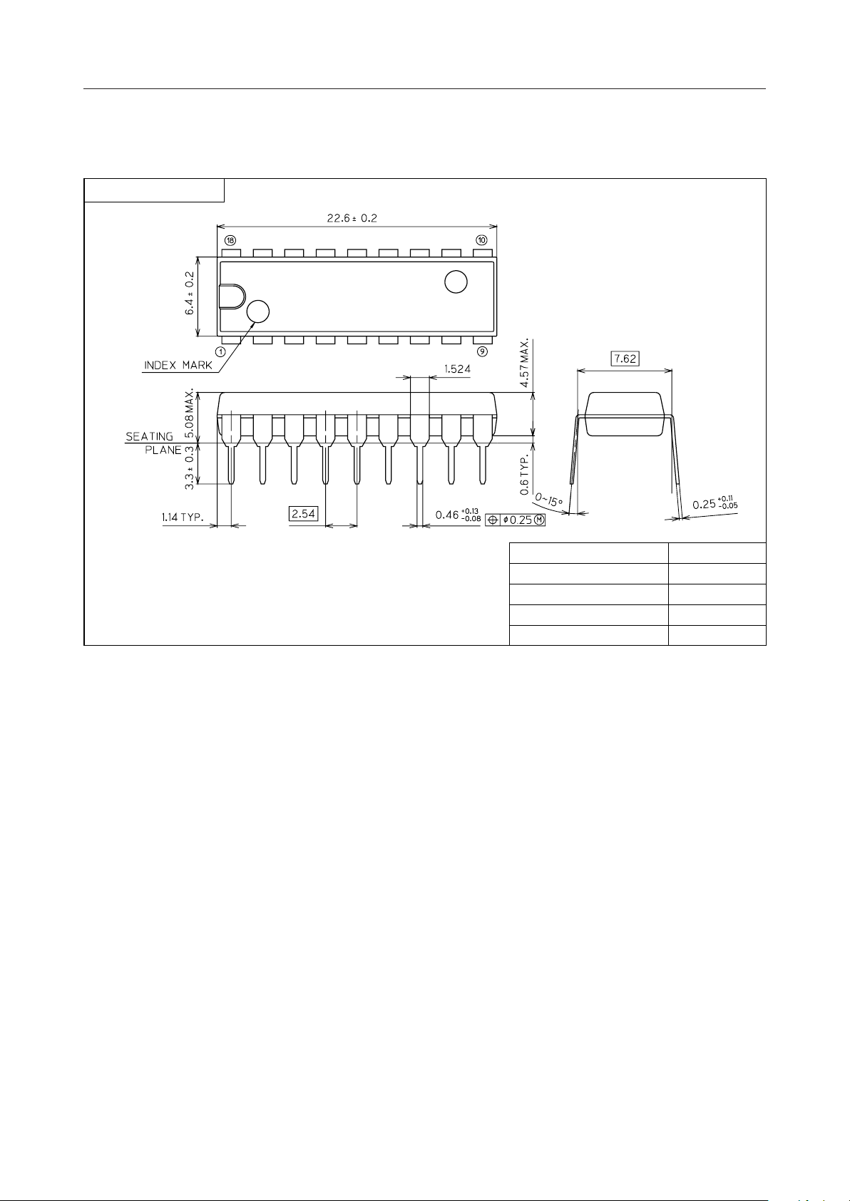
PACKAGE DIMENSIONS
DIP18-P-300-2.54
MSM9802/03/05-xxx¡ Semiconductor
(Unit : mm)
Package material
Lead frame material
Pin treatment
Solder plate thickness
Package weight (g)
Epoxy resin
42 alloy
Solder plating
5 mm or more
1.30 TYP.
49/51
Page 50
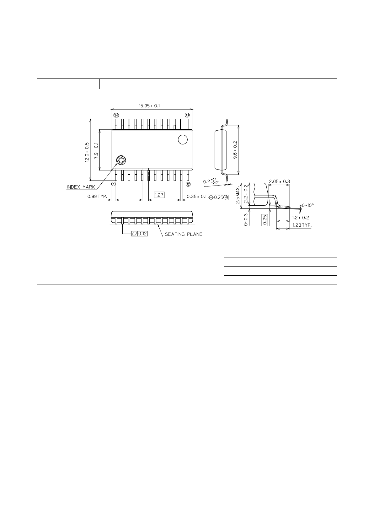
SOP24-P-430-1.27-K
Mirror finish
MSM9802/03/05-xxx¡ Semiconductor
(Unit : mm)
Package material
Lead frame material
Pin treatment
Solder plate thickness
Package weight (g)
Epoxy resin
42 alloy
Solder plating
5 mm or more
0.58 TYP.
Notes for Mounting the Surface Mount Type Package
The SOP, QFP, TSOP, TQFP, LQFP, SOJ, QFJ (PLCC), SHP, and BGA are surface mount type
packages, which are very susceptible to heat in reflow mounting and humidity absorbed in
storage. Therefore, before you perform reflow mounting, contact Oki’s responsible sales person
on the product name, package name, pin number, package code and desired mounting conditions
(reflow method, temperature and times).
50/51
Page 51
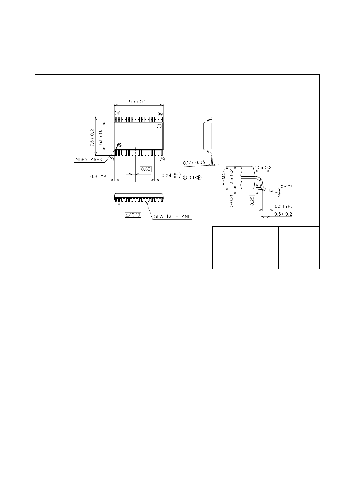
SSOP30-P-56-0.65-K
Mirror finish
MSM9802/03/05-xxx¡ Semiconductor
(Unit : mm)
Package material
Lead frame material
Pin treatment
Solder plate thickness
Package weight (g)
Epoxy resin
42 alloy
Solder plating
5 mm or more
0.19 TYP.
Notes for Mounting the Surface Mount Type Package
The SOP, QFP, TSOP, TQFP, LQFP, SOJ, QFJ (PLCC), SHP, and BGA are surface mount type
packages, which are very susceptible to heat in reflow mounting and humidity absorbed in
storage. Therefore, before you perform reflow mounting, contact Oki’s responsible sales person
on the product name, package name, pin number, package code and desired mounting conditions
(reflow method, temperature and times).
51/51
Page 52

E2Y0002-29-62
NOTICE
1. The information contained herein can change without notice owing to product and/or
technical improvements. Before using the product, please make sure that the information
being referred to is up-to-date.
2. The outline of action and examples for application circuits described herein have been
chosen as an explanation for the standard action and performance of the product. When
planning to use the product, please ensure that the external conditions are reflected in the
actual circuit, assembly, and program designs.
3. When designing your product, please use our product below the specified maximum
ratings and within the specified operating ranges including, but not limited to, operating
voltage, power dissipation, and operating temperature.
4. Oki assumes no responsibility or liability whatsoever for any failure or unusual or
unexpected operation resulting from misuse, neglect, improper installation, repair, alteration
or accident, improper handling, or unusual physical or electrical stress including, but not
limited to, exposure to parameters beyond the specified maximum ratings or operation
outside the specified operating range.
5. Neither indemnity against nor license of a third party’s industrial and intellectual property
right, etc. is granted by us in connection with the use of the product and/or the information
and drawings contained herein. No responsibility is assumed by us for any infringement
of a third party’s right which may result from the use thereof.
6. The products listed in this document are intended for use in general electronics equipment
for commercial applications (e.g., office automation, communication equipment,
measurement equipment, consumer electronics, etc.). These products are not authorized
for use in any system or application that requires special or enhanced quality and reliability
characteristics nor in any system or application where the failure of such system or
application may result in the loss or damage of property, or death or injury to humans.
Such applications include, but are not limited to, traffic and automotive equipment, safety
devices, aerospace equipment, nuclear power control, medical equipment, and life-support
systems.
7. Certain products in this document may need government approval before they can be
exported to particular countries. The purchaser assumes the responsibility of determining
the legality of export of these products and will take appropriate and necessary steps at their
own expense for these.
8. No part of the contents contained herein may be reprinted or reproduced without our prior
permission.
9. MS-DOS is a registered trademark of Microsoft Corporation.
Copyright 1999 Oki Electric Industry Co., Ltd.
Printed in Japan
 Loading...