

Page 1

E2B0014-27-Y2
¡ Semiconductor MSM9004-01/02
¡ Semiconductor
This version: Nov. 1997
Previous version: Mar. 1996
MSM9004-01/02
1/3, 1/4 DUTY LCD DRIVER WITH 4-DOT COMMON DRIVER AND 49-DOT SEGMENT DRIVER
GENERAL DESCRIPTION
The MSM 9004-01/02 is an LCD driver for dynamic display with a 1/3 or 1/4 duty select function.
When the 1/3 duty is selected, it can display up to 147 segments, and when the 1/4 duty is
selected, up to 196 segments.
FEATURES
• Logic power supply voltage (V
• LCD drive power supply voltage (V
• Serial transfer clock frequency : 2 MHz max.
• LCD output resistance
Common driver : 20 kW
Segment driver : 60 kW
• Display duty : 1/3, 1/4 selectable
• LCD segment output : 49
• Maximum number of display segments
For 1/3 duty : 147 segments max.
For 1/4 duty : 196 segments max.
• Display blanking terminal attached
• Operating temperature range : –40 to +85˚C
• Interface with microcontroller
MSM9004-01 : LOAD, DATA, CLOCK1, CLOCK2
MSM9004-02 : LOAD, DATA, CLOCK2
• System clock
MSM9004-01 : external input
MSM9004-02 : internal oscillation circuit (external resistor
• Package:
64-pin plastic QFP (QFP64-P-1414-0.80-BK) (Product name : MSM9004-01GS-BK)
• Comparison of device codes and functions
) : 5.0 V ± 10%
DD
) : 3.7 V to 5.5 V
LCD
and capacitor required)
(Product name : MSM9004-02GS-BK)
Function
Device code
MSM9004-01
MSM9004-02
MSM9004-03
MSM9004-04
LCD segment
output
50 49
—
—
—
—
Duty
1/3 1/4 External input
—
—
System clock
—
—
Internal oscillation
circuit
—
—
1/15
Page 2

¡ Semiconductor MSM9004-01/02
BLOCK DIAGRAM
MSM9004-01
SEG49SEG1
V
DD
V
BLANK
49-DOT SEGMENT DRIVER
LC1
V
LC2
V
LC3
3/4SEL
CLOCK1
LOAD
CLOCK2
DATA
TIMING
GENERATOR
49-BIT
DATA LATCH 1
CONTROL
LOGIC
49-BIT DATA SELECTOR
49-BIT
DATA LATCH 2
49-BIT
DATA LATCH 3
49-BIT SHIFT REGISTER
COMMON
DRIVER
49-BIT
DATA LATCH 4
COM1
COM2
COM3
COM4
V
DD
V
SS
2/15
Page 3

¡ Semiconductor MSM9004-01/02
BLOCK DIAGRAM
MSM9004-02
SEG49SEG1
V
DD
V
BLANK
49-DOT SEGMENT DRIVER
LC1
V
LC2
V
LC3
3/4SEL
OSC
LOAD
CLOCK2
DATA
TIMING
GENERATOR
49-BIT
DATA LATCH 1
OSCILLATOR
CONTROL
LOGIC
49-BIT DATA SELECTOR
49-BIT
DATA LATCH 2
49-BIT
DATA LATCH 3
49-BIT SHIFT REGISTER
COMMON
DRIVER
49-BIT
DATA LATCH 4
COM1
COM2
COM3
COM4
V
DD
V
SS
3/15
Page 4

¡ Semiconductor MSM9004-01/02
MSM9004-01
SEG1
SEG2
SEG3
SEG4
SEG5
SEG6
SEG7
SEG8
SEG9
SEG10
SEG11
10
11
12SEG12
13SEG13
14SEG14
15SEG15
16SEG16
COM4
COM3
COM2
64
63
62
1
2
3
4
5
6
7
8
9
LC1VLC2VLC3VSS
COM1
V
61
60
59
58
57
CLOCK1
VDD3/4SEL
56
55
54
53 LOAD
52 DATA
51 CLOCK2
50 BLANK
49 SEG49
48
47
46
45
44
43
42
41
40
39
38
37 SEG37
36 SEG36
35 SEG35
34 SEG34
33 SEG33
SEG48
SEG47
SEG46
SEG45
SEG44
SEG43
SEG42
SEG41
SEG40
SEG39
SEG38
17
18
SEG17
SEG18
19
20
SEG19
SEG20
21
22
23
24
25
SEG21
SEG22
SEG23
SEG24
SEG25
64-Pin Plastic QFP
26
27
SEG26
SEG27
28SEG28
29SEG29
30SEG30
31SEG31
32SEG32
4/15
Page 5

¡ Semiconductor MSM9004-01/02
PIN CONFIGURATION (TOP VIEW)
MSM9004-02
SEG1
SEG2
SEG3
SEG4
SEG5
SEG6
SEG7
SEG8
SEG9
SEG10
SEG11
1
2
3
4
5
6
7
8
9
10
11
12SEG12
13SEG13
14SEG14
15SEG15
16SEG16
COM4
COM3
64
63
COM2
COM1
62
61
LC1VLC2VLC3VSS
V
60
59
58
57
OSC
VDD3/4SEL
56
55
54
53 LOAD
52 DATA
51 CLOCK2
50 BLANK
49 SEG49
48
47
46
45
44
43
42
41
40
39
38
37 SEG37
36 SEG36
35 SEG35
34 SEG34
33 SEG33
SEG48
SEG47
SEG46
SEG45
SEG44
SEG43
SEG42
SEG41
SEG40
SEG39
SEG38
17
18
SEG17
SEG18
19
20
SEG19
SEG20
21
22
23
24
25
SEG21
SEG22
SEG23
SEG24
SEG25
64-Pin Plastic QFP
26
27
SEG26
SEG27
28SEG28
29SEG29
30SEG30
31SEG31
32SEG32
5/15
Page 6
¡ Semiconductor MSM9004-01/02
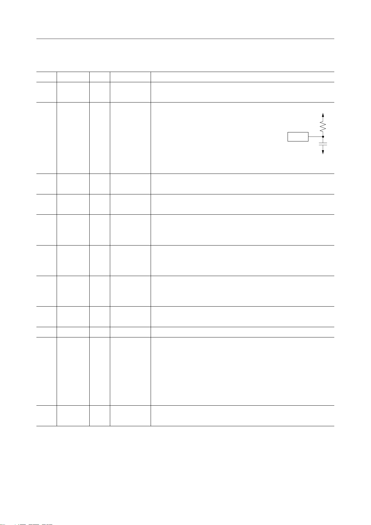
PIN DESCRIPTIONS
Pin Symbol Type
56 I Micro-
CLOCK1
*1
Connected to
controller
56 I External
OSC
*2
resistor
Capacitor
52 I Micro-
DATA
controller
51 I Micro-
CLOCK2
controller
53 I Micro-
LOAD
controller
50 I
BLANK
54 I
3/4SEL
61 to 64 O LCD
1 to 49 O LCD
COM1-4
SEG1-49
60 Power
V
LC1
59
58
V
LC2
V
LC3
supply
—
—
—
Description
System clock input pin.
For details, see "MSM9004-02 Oscillation Circuit Characteristics".
Pin for oscillation.
V
DD
Connecting the external resistor and capacitor to
configure the oscillation circuit.
Connect the resistor and capacitor as shown in the
OSC
right figure.
V
Make the length of wiring between this pin and the
SS
external resistor and capacitor as short as passible.
Serial data input.
For details on the configuration of input data, see "Data Configuration".
Shift clock input (Schmitt circuit included).
Input data is read synchronizing with the rising edge of this clock.
Load signal input (Schmitt circuit included).
Serial input data is transferred to the display latch when this LOAD
signal is at a "H" level.
Input pin for turning off all segments.
All segments turn off, regardless of the display data, when this pin is
at a "L" level, and all segments return to the status before turning off.
Input pin for selecting 1/3 or 1/4 duty.
1/3 duty drive is selected when this pin is at a "H" level, and 1/4 duty
drive is selected when this pin is at a "L" level.
LCD common outputs.
Leave COM4 open for 1/3 duty drive.
LCD segment outputs.
Bias power supply pins for driving the LCD.
Conditions for bias voltage are as follows :
– V
1
LC3
£ 5.5V
LC3
)
3.7V £ V
V
DD
= VDD – 3 (VDD – V
LC1
2
= VDD – 3 (VDD – V
V
LC2
LC3
)
55 Power
V
DD
57
V
SS
supply
*1: Applied to MSM9004-01.
*2: Applied to MSM9004-02.
—
≥ V
V
LC3
SS
Power supply pins.
Normally used as V
= 4.5 to 5.5 V and Vss = 0 V.
DD
6/15
Page 7
¡ Semiconductor MSM9004-01/02
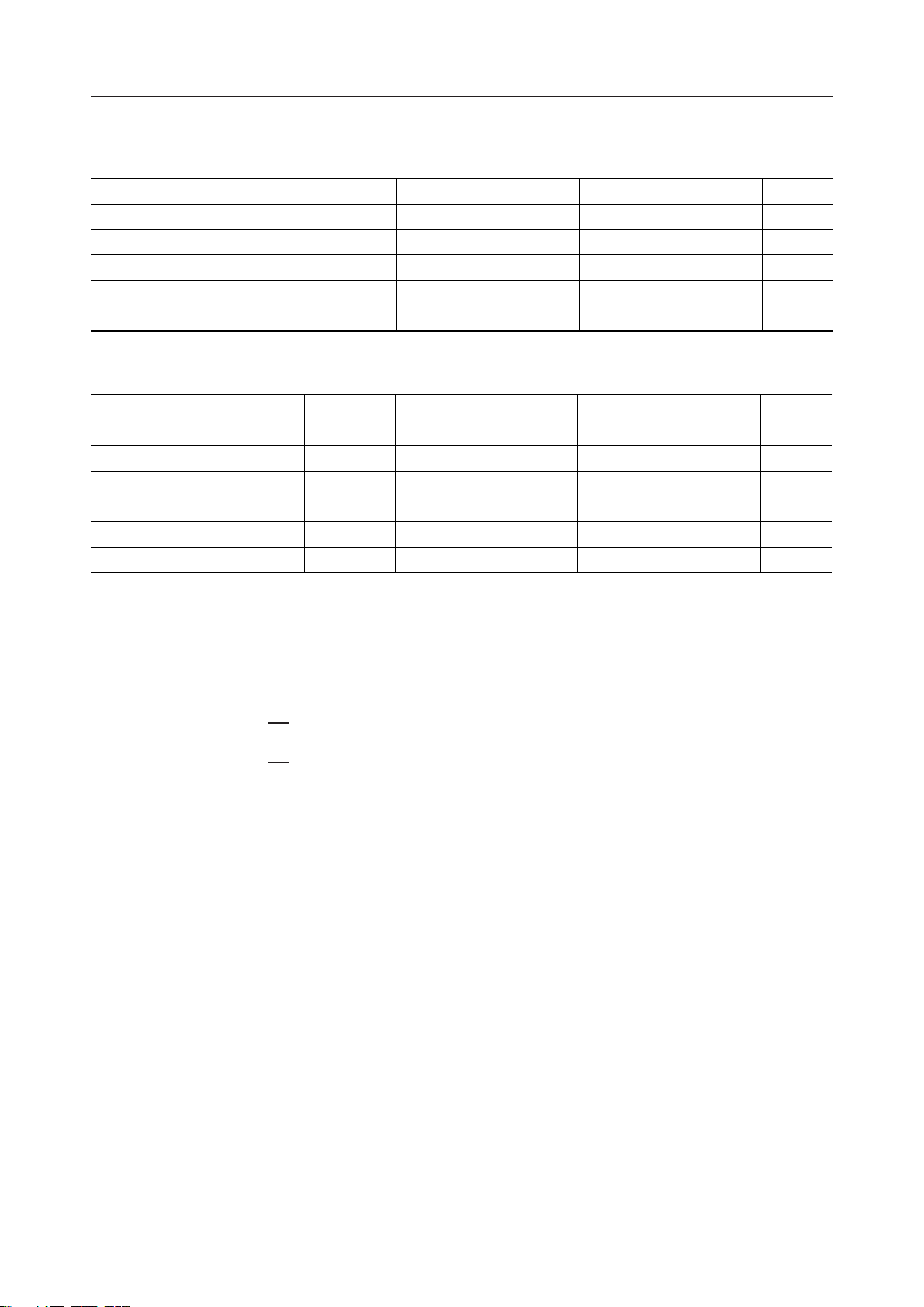
ABSOLUTE MAXIMUM RATINGS
Parameter Symbol Condition Rating Unit
Power Supply Voltage V
LCD Driver Voltage V
Input Voltage V
Power Dissipation P
Storage Temperature T
DD
LCD
IN
D
STG
— –0.3 to +6.5 V
— –0.3 to VDD +0.3 V
— –0.3 to VDD +0.3 V
Ta = +85˚C 450 mW
— –55 to 150 °C
RECOMMENDED OPERATING CONDITIONS
Parameter Symbol Condition Range Unit
Power Supply Voltage V
LCD Driver Voltage V
System Clock Frequency f
Self Oscillation Frequency f
Shift Frequency (Max) f
Operating Temperature T
DD
* 1 * 3
LCD
CP1
OSC
CP2
op
Applied to MSM9004-01
Applied to MSM9004-02
— 4.5 to 5.5 V
* 2
3.7V to V
DD
V
1.5 to 4.3 kHz
1.5 to 4.3 kHz
— 2.0 MHz
— –40 to +85 °C
*1: VDD–V
LC3
*2: The following relationship must be kept:
VDD>V
V
V
V
LC1>VLC2≥VSS
LC1=VDD
LC2=VDD
LC3=VDD
1
–(V
–(V
–(V
3
2
3
3
3
DD – VLC3
DD – VLC3
DD – VLC3
)
)
)
*3: VDD is the reference potential for the LCD driving voltage. To decide the LCD driving
voltage, change the voltage between V
LC3
and V
SS (VLC3
> 0).
7/15
Page 8
¡ Semiconductor MSM9004-01/02
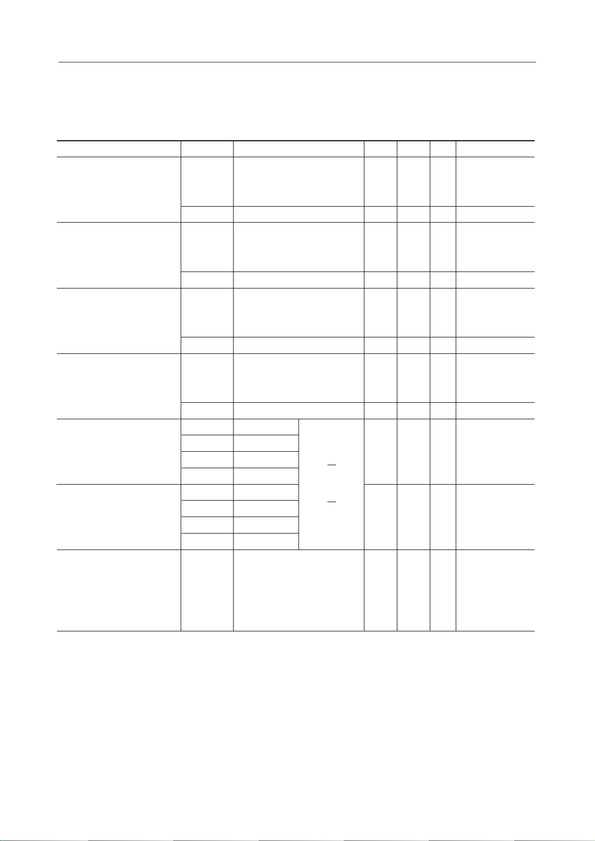
ELECTRICAL CHARACTERISTICS
DC Characteristics (MSM9004-01)
Parameter Symbol Condition Min. Max. Unit Applicable pin
"H" Input Voltage
V
IH1
V
IH2
"L" Input Voltage
V
IL1
V
IL2
"H" Input Current
I
IH1
I
IH2
"L" Input Current
I
IL1
I
IL2
R
ONV0
R
ON Resistance (SEG)
ON Resistance (COM)
Dynamic Supply Current
R
R
R
R
R
R
ONV1
ONV2
ONV3
ONV0
ONV1
ONV2
ONV3
I
DD
(Ta= –40 to +85°C, V
—
—
— 0.0
— 0.0
VIN=V
DD
VIN=V
DD
=4.5 to 5.5 V, VDD–V
DD
0.8VDDV
0.85VDDV
0.2V
DD
DD
DD
0.15VDDV CLOCK1
–1.0 1.0 mA
–3.0 3.0 mA BLANK
VDD=5.5 V, VIN=0 V –1.0 1.0 mA
VDD=5.5 V, VIN=0 V –160 –20 mA BLANK
=–10 mA
I
O
V
DD
=4.5 V
IO=±10 mA
=±10 mA
I
O
= 10 mA
I
O
=–30 mA
I
O
I
=±30 mA
O
=±30 mA
I
O
= 30 mA
I
O
f
=2.4 kHz * 1
CP1
=1 MHz
f
CP2
1/4 duty
= V
V
LC1
V
= V
LC2
V
LC3=VSS
2
DD
3
1
DD
3
—60kWSEG1-49
—20kWCOM1-4
— 0.65 mA V
COM1-4 : No Load
SEG1-49 : No Load
=3.7 V to VDD)
LC3
LOAD, CLOCK2
DATA, 3/4SEL
V
BLANK
V CLOCK1
LOAD, CLOCK2
DATA, 3/4SEL
V
BLANK
LOAD, CLOCK1
CLOCK2, DATA
3/4SEL
LOAD, CLOCK1
CLOCK2, DATA
3/4SEL
DD
* 1 For input data, input a logic "0" and a logic "1" to LCD display bits alternately.
The tr and tf time for the CLOCK1, CLOCK2, DATA and LOAD pins must be less than
20ns.
8/15
Page 9
¡ Semiconductor MSM9004-01/02
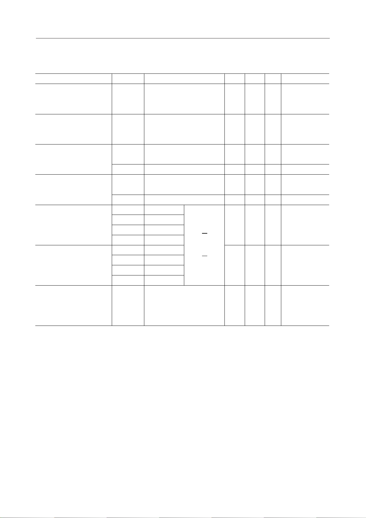
DC Characteristics (MSM9004-02)
Parameter Symbol Condition Min. Max. Unit Applicable pin
"H" Input Voltage
"L" Input Voltage
"H" Input Current
"L" Input Current
R
R
ON Resistance (SEG)
R
R
R
R
ON Resistance (COM)
R
R
Dynamic Supply Current I
V
IH1
V
IL1
I
IH1
I
IH2
I
IL1
I
IL2
ONV0
ONV1
ONV2
ONV3
ONV0
ONV1
ONV2
ONV3
DD
(Ta= –40 to +85°C, V
—
— 0.0
VIN=V
DD
VIN=V
DD
=4.5 to 5.5 V, VDD–V
DD
0.8VDDV
0.2V
DD
DD
–1.0 1.0 mA
–3.0 3.0 mA BLANK
VDD=5.5 V, VIN=0 V –1.0 1.0 mA
VDD=5.5 V, VIN=0 V –160 –20 mA BLANK
IO=–10 mA
V
DD
=4.5 V
IO=±10 mA
=±10 mA
I
O
= 10 mA
I
O
=–30 mA
I
O
I
=±30 mA
O
=±30 mA
I
O
= 30 mA
I
O
f
=1 MHz
CP2
1/4 duty
= V
V
LC1
V
= V
LC2
V
LC3=VSS
2
DD
3
1
DD
3
—60kWSEG1-49
—20kWCOM1-4
*1
— 1.00 mA V
COM1-4 : No Load
SEG1-49 : No Load
=3.7 V to VDD)
LC3
LOAD, CLOCK2
DATA, 3/4SEL
V
BLANK
LOAD, CLOCK2
DATA, 3/4SEL
V
BLANK
LOAD, CLOCK2
DATA,
LOAD, CLOCK2
DATA,
DD
3/4SEL
3/4SEL
* 1: For input data, input a logic "0" and a logic "1" to LCD display bits alternately.
External resistor for oscillation : RO = 62 kW
External capacitor for oscillation : CO = 0.01 mF
The tr, and tf time for the CLOCK2, DATA and LOAD pins must be less than 20ns.
The current that flows through the external resistor and capacitor is not included.
9/15
Page 10
¡ Semiconductor MSM9004-01/02
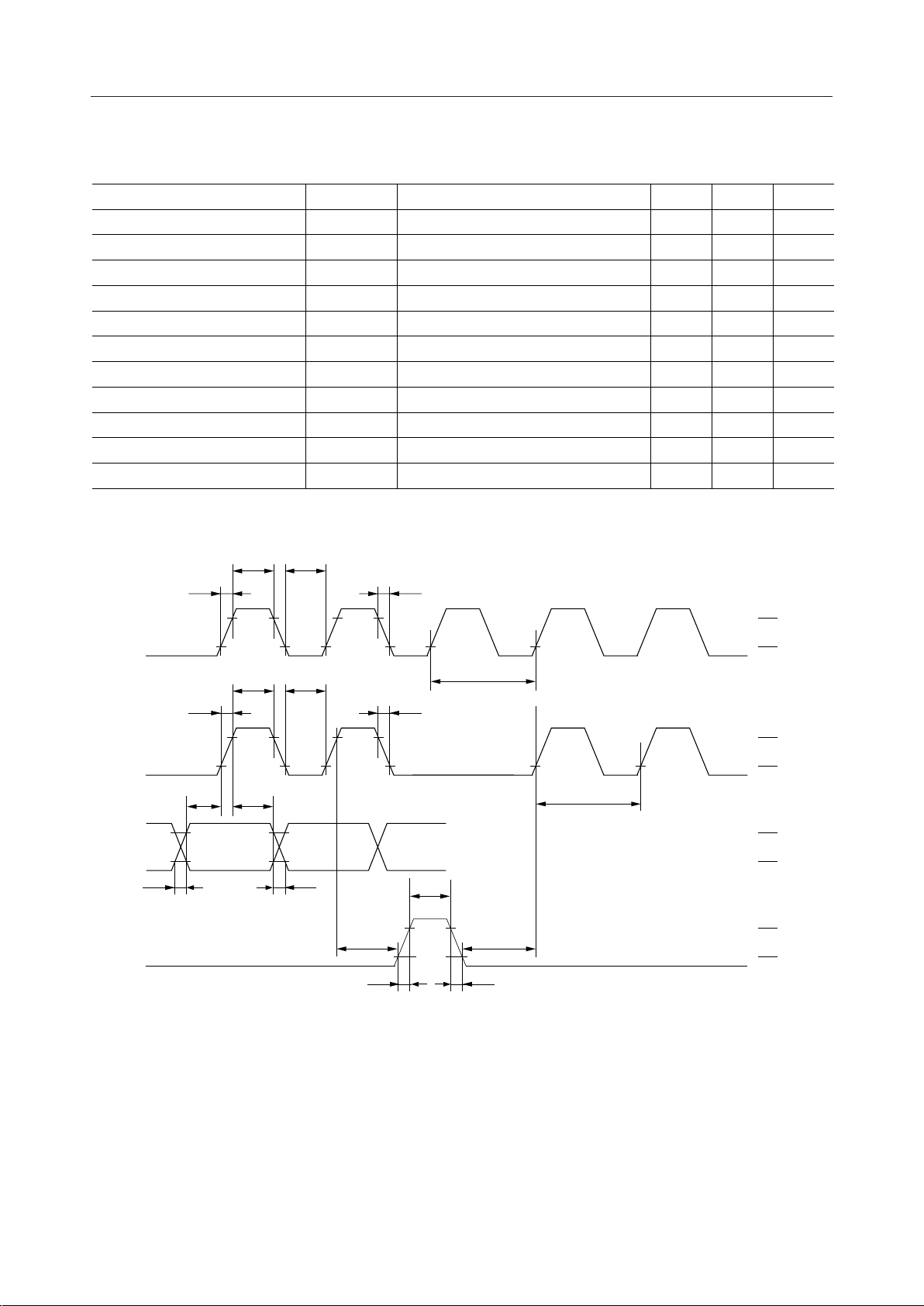
AC Characteristics
Parameter Symbol Condition Min. Max. Unit
System Clock Frequency f
System Clock Pulse Width t
WCP1
Data Clock Frequency f
Data Clock Pulse Frequency t
WCP2
Data Setup Time t
Data Hold Time t
Load Pulse Width t
Clock-Load Time t
Load-Clock Time t
Rise Time t
Fall Time t
CP1
CP2
SU
HD
WLD
CL
LC
r
f
(Ta= –40 to +85°C, V
Not applied to MSM9004-02 1.5 4.3 kHz
Not applied to MSM9004-02 1.0 — ms
=4.5 to 5.5 V, VDD–V
DD
= 3.7 V to VDD)
LC3
— 2.0 MHz—
200 — ns—
100 — ns—
100 — ns—
200 — ns—
200 — ns—
200 — ns—
— 100 ns—
— 100 ns—
CLOCK1
* 1
CLOCK2
DATA
LOAD
tw
t
r
tw
t
r
t
SU
t
r
tw
CP1
CP2
t
HD
tw
CP1
CP2
t
f
t
f
0.85V
DD
0.15V
DD
1/f
CP1
t
f
0.8V
DD
0.2V
DD
1/f
CP2
0.8V
DD
0.2V
DD
t
WLD
0.8V
0.2V
DD
DD
t
CL
t
r
t
LC
t
f
*1 Not applied to MSM9004-02.
10/15
Page 11
¡ Semiconductor MSM9004-01/02
FUNCTIONAL DESCRIPTION
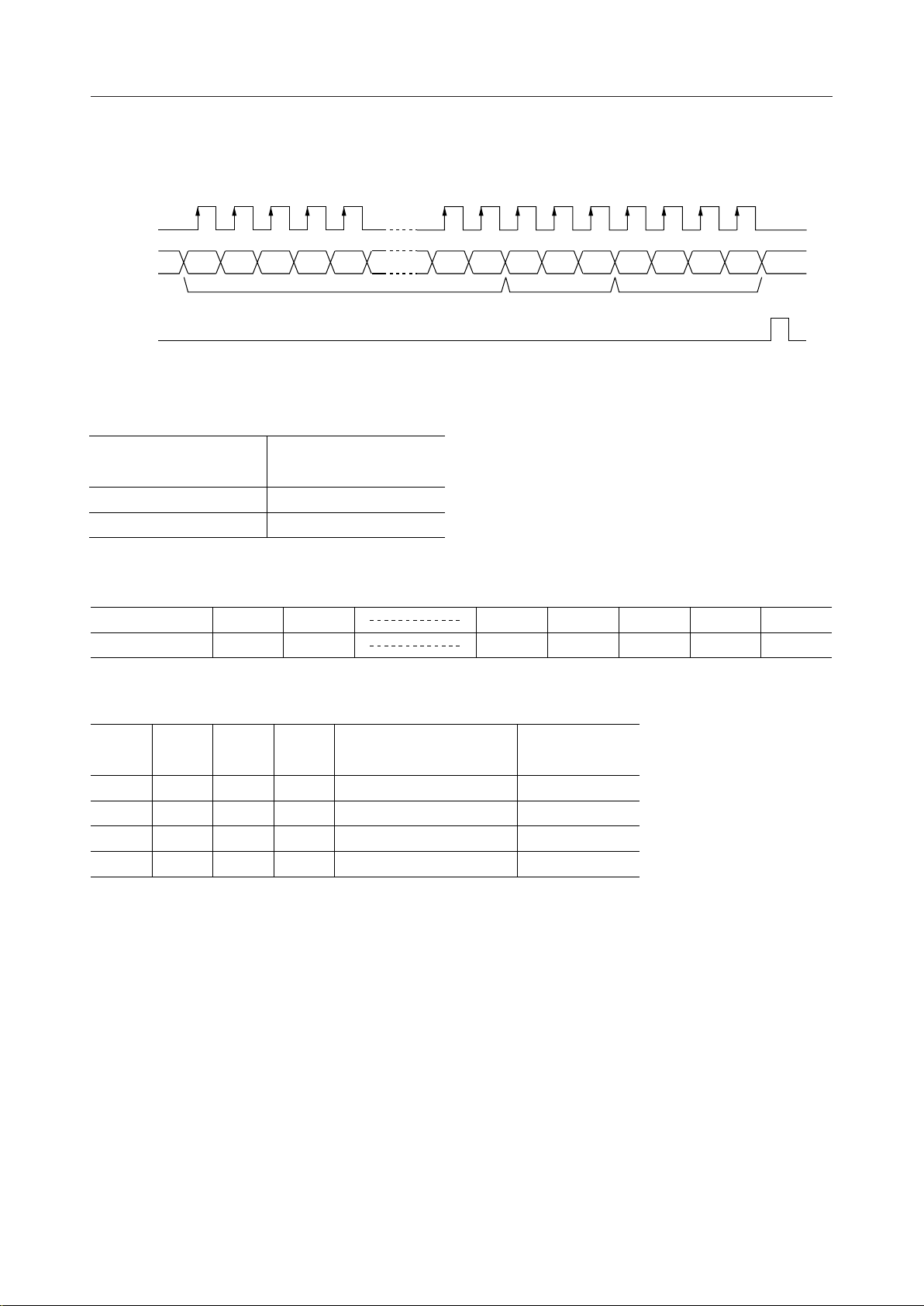
Display Data Input
CLOCK2
DATA
LOAD
D48 D47 D46 D45 D2D49 D1 0 0 0 C1 C2 C3 C4
LCD display bit
(49 bits)
Dummy bit
(3 bits)
Note: Always set a logic "0" to the dummy bit.
LCD Display Bit - LCD Panel Lighting Status Correspondence Table
LCD display bit
(D1 to D49)
1ON
0 OFF
LCD panel lighting
status
LCD Display Bit - Segment Output Correspondence Table
LCD display bit
Segment output
D1
SEG1
D2
SEG2
D45
SEG45
D46
SEG46
D47
SEG47
Select Bit - Data Latch Correspondence Table
Select bit
(4 bits)
D48
SEG48
D49
SEG49
C4 C3 C2 C1
0001
0010
0100
1000
Display data writing
data latch
Data latch 1
Data latch 2
Data latch 3
Data latch 4
Corresponding
common output
COM1
COM2
COM3
COM4
The select bits C1 to C4 select Data latch 1 to Data latch 4 corresponding to COM 1 to COM 4
independently. If logic "1s" are selected to multiple select bits, the LCD display bits are written
to all corresponding data latches.
Example:
When logic "1s" are set to all select bits C1 to C4, and logic "0s" are set to all LCD display bits D1
to D49, logic "0s" are written to Data latch 1 to Data latch 4 by one data input. This leads to turning
off the entire LCD panel.
11/15
Page 12
¡ Semiconductor MSM9004-01/02
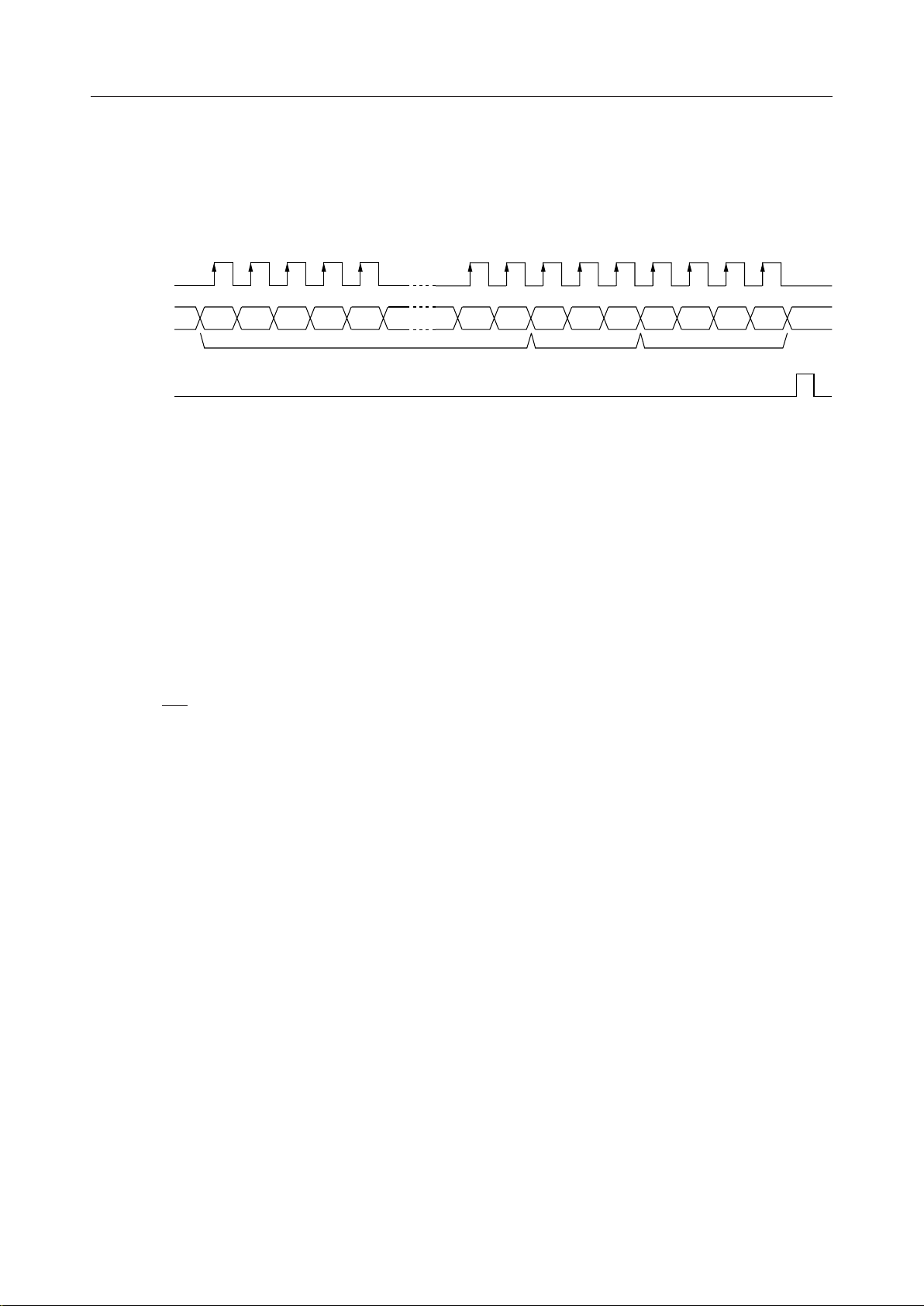
How to Decrease Transfer Time When Unused Segments Exist
The MSM9004-01/02 can operate even if segment data is not full. Input data as shown in the
figure below. In this case, the last 4 bits are the select bits.
Transfer example: for 30 segments
CLOCK2
DATA
LOAD
D29 D28 D27 D26 D2D30 D1 0 0 0 C1 C2 C3 C4
LCD display bits
(30 bits)
Dummy bits
(3 bits)
Select bits
(4 bits)
Note: Always set "0" to the dummy bits.
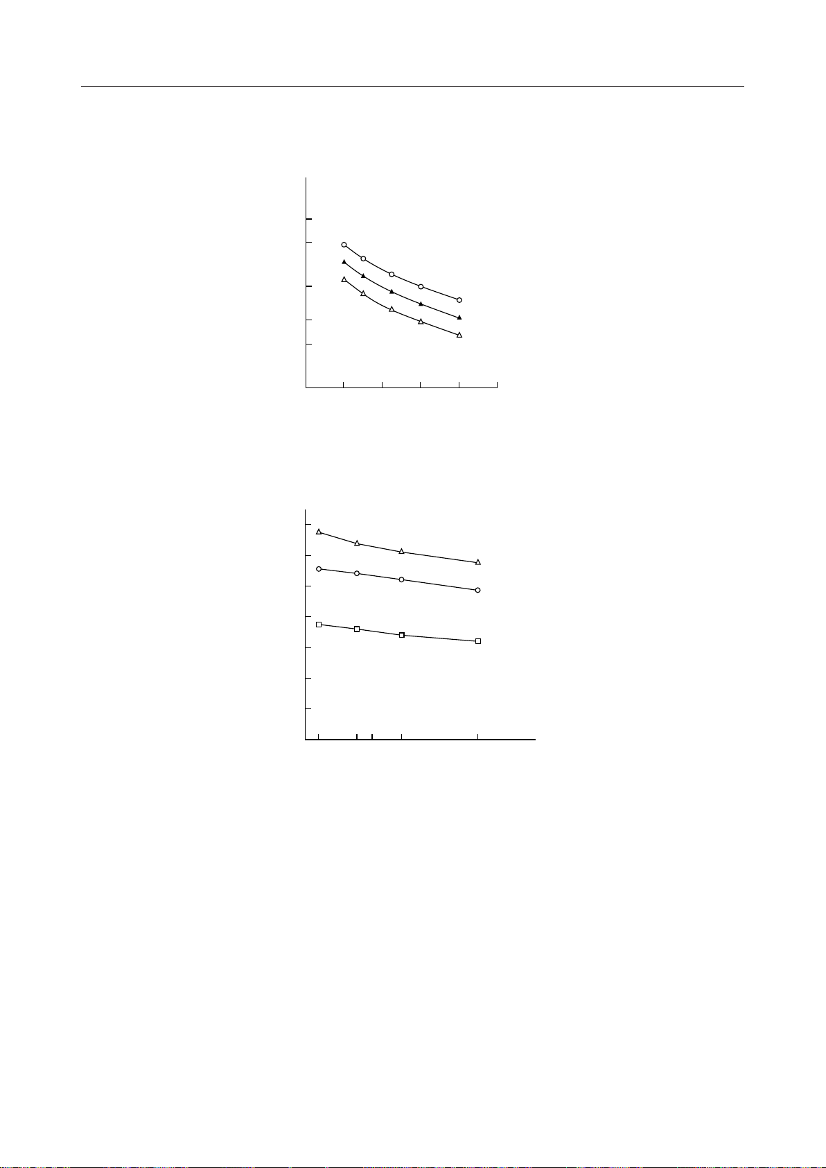
Recommended RC Values for MSM9004-02 Oscillation Circuit
Shown below are the recommended oscillation resistor (RO) and capacitor (CO) values for
providing frame frequency f
• R
= 62 kW ±5%
O
• C
= 0.01 mF ±5%
O
of approximately 62 Hz to 190 Hz.
FRM
(Resistance and capacitance variations due to temperature change are not included.)
For requirements of supply voltage (VDD), ambient temperature range (Ta), and frame frequency
(f
):
FRM
• VDD = 5.0 V
• Ta = –40 to +85°C
• f
FRM
1
= oscillation frequency
24
12/15
Page 13
¡ Semiconductor MSM9004-01/02
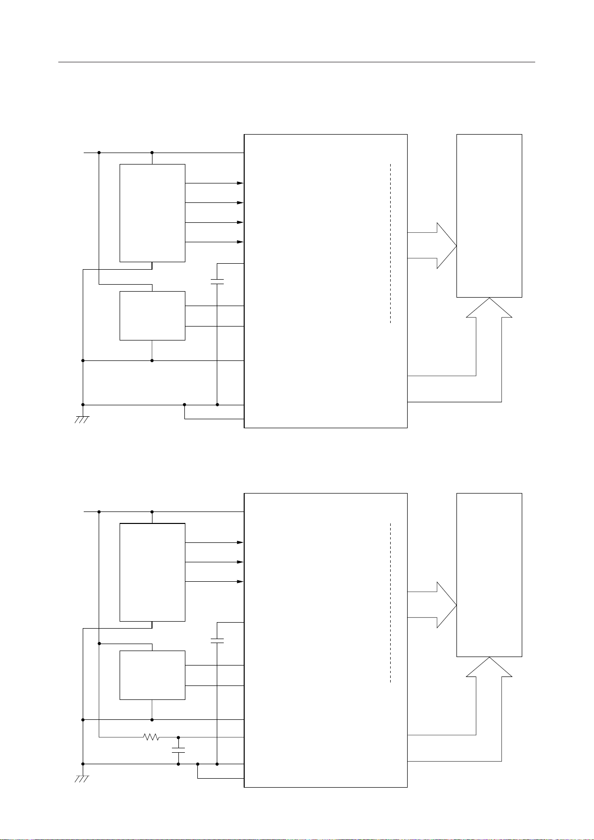
APPLICATION CIRCUITS
MSM9004-01
+5 V
V
DD
Output
Port
CPU
V
SS
BIAS
CIRCUIT
V
DD
DATA
CLOCK2
LOAD
CLOCK1
BLANK
V
LC1
V
LC2
V
LC3
V
SS
3/4SEL
SEG1
1/4 DUTY
LCD
PANEL
MSM9004-01
SEG49
COM1
COM2
COM3
COM4
MSM9004-02
+5 V
V
DD
Output
Port
CPU
V
SS
BIAS
CIRCUIT
R
0
V
DD
DATA
CLOCK2
LOAD
SEG1
1/4 DUTY
LCD
PANEL
BLANK
MSM9004-02
V
LC1
V
LC2
V
LC3
OSC
C
0
V
SS
3/4SEL
SEG49
COM1
COM2
COM3
COM4
13/15
Page 14
¡ Semiconductor MSM9004-01/02
REFERENCE DATA
f
vs. R
FRM
500
300
[Hz]
FRM
100
50
30
Frame Frequency f
0
VDD = 5 V
Ta = 25˚C
= 0.01 mF
C
O
C
= 0.015 mF
O
= 0.022 mF
C
O
10
20 40 60 80
140
120
[Hz]
100
FRM
80
60
40
Frame Frequency f
20
-40
-10 25 850
Resistance R
f
vs. Ta
FRM
Temperature Ta [˚C]
[kW]
O
VDD = 5 V
RO = 33 kW
C
= 0.015 mF
O
= 62 kW
R
O
C
= 0.01 mF
O
R
= 62 kW
O
C
= 0.015 mF
O
14/15
Page 15
¡ Semiconductor MSM9004-01/02
PACKAGE DIMENSIONS
(Unit : mm)
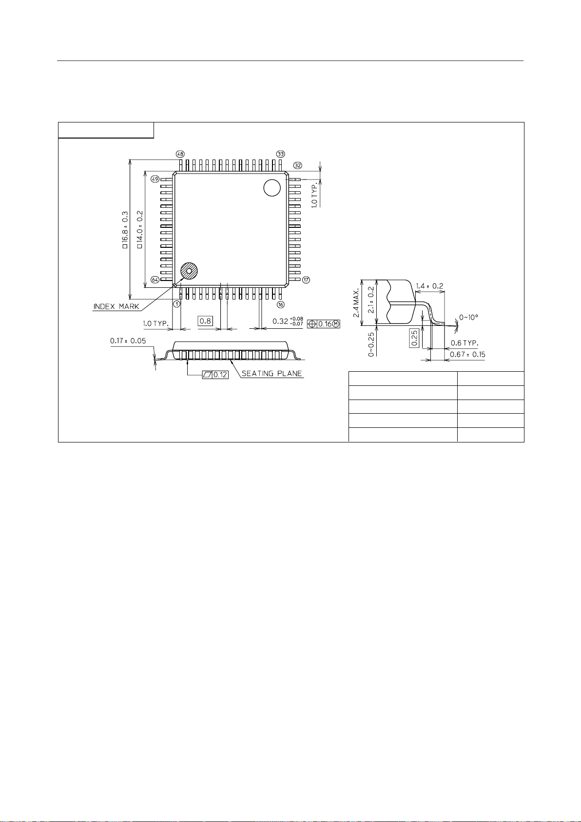
QFP64-P-1414-0.80-BK
Mirror finish
Package material
Lead frame material
Pin treatment
Solder plate thickness
Package weight (g)
Epoxy resin
42 alloy
Solder plating
5 mm or more
0.87 TYP.
Notes for Mounting the Surface Mount Type Package
The SOP, QFP, TSOP, SOJ, QFJ (PLCC), SHP and BGA are surface mount type packages, which
are very susceptible to heat in reflow mounting and humidity absorbed in storage.
Therefore, before you perform reflow mounting, contact Oki’s responsible sales person for the
product name, package name, pin number, package code and desired mounting conditions
(reflow method, temperature and times).
15/15
 Loading...