

Page 1

E2E0016-38-93
¡ Semiconductor
This version: Sep. 1998
Previous version: Mar. 1996
MSM6422¡ Semiconductor
MSM6422
High speed and Simple 4-Bit Microcontroller
GENERAL DESCRIPTION
The MSM6422 is a low-power, single-chip device implemented in complementary metal-oxide
semiconductor technology.
The MSM6422 can be used in place of logic ICs configured around a main CPU, or for small-scale
systems such as home electronic equipment.
FEATURES
• ROM : 2048 words ¥ 8 bits
• RAM : 64 words ¥ 4 bits
• I/O port
Input-output port : 4 ports ¥ 4 bits (pseudo bidirectional configuration)
1 port ¥ 2 bits (pseudo bidirectional configuration)
Input port : 1 port ¥ 1 bit (combined use with an interrupt input)
• Instructions : 63
• Two interrupt sources (1 internal, 1 external)
• Power down features
• Minimum instruction execution time : 952 ns @ 4.2 MHz clock
• Crystal and ceramic oscillation
• Single 5 V power supply
• Package options:
24-pin plastic DIP (DIP24-P-600-2.54) : (Product name : MSM6422-¥¥RS)
24-pin plastic SOP (SOP24-P-430-1.27-K) : (Product name : MSM6422-¥¥GS-K)
¥¥ indicates a code number.
1/10
Page 2
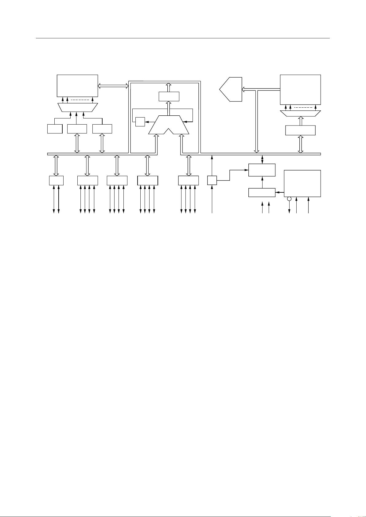
BLOCK DIAGRAM
MSM6422¡ Semiconductor
RAM
64 ¥ 4 bits
DEC
3 21 010
ACC
C
ALU
HRLRSP
3210 3210 3210
INST
DEC
ROM
2048 ¥ 8 bits
DEC
PC
INT.C
P0P1P3P4P5
P2
12-bitTBC
0/INT
GND V
DD
Timing
&
Control
OSC1 OSC0
RESET
2/10
Page 3
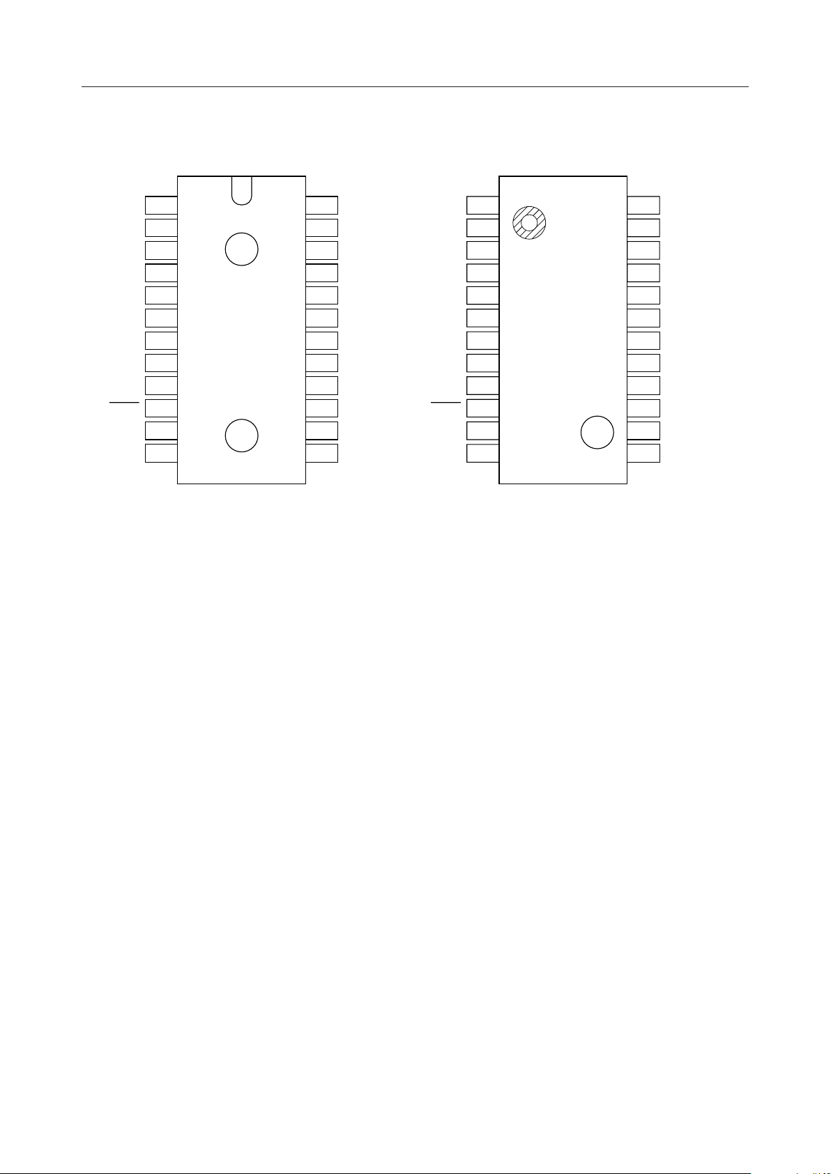
PIN CONFIGURATION (TOP VIEW)
MSM6422¡ Semiconductor
P2.0/INT
P0.0
P0.1
P0.2
P0.3
P1.0
P1.1
P1.2
P1.3
OSC
OSC
GND
1
2
3
4
5
6
7
8
9
10
1
11
0
12
24
23
22
21
20
19
18
17
16
15
14
13
V
DD
P5.1
P5.0
P4.3
P4.2
P4.1
P4.0
P3.3
P3.2
P3.1
P3.0
RESET
P2.0/INT
P0.0
P0.1
P0.2
P0.3
P1.0
P1.1
P1.2
P1.3
OSC
OSC
GND
24-Pin Plastic DIP
1
2
3
4
5
6
7
8
9
10
1
11
0
12
24
23
22
21
20
19
18
17
16
15
14
13
V
DD
P5.1
P5.0
P4.3
P4.2
P4.1
P4.0
P3.3
P3.2
P3.1
P3.0
RESET
24-Pin Plastic SOP
3/10
Page 4

PIN DESCRIPTIONS
MSM6422¡ Semiconductor
Pin
2
3
4
5
6
7
8
9
14
15
16
17
18
19
20
21
22
23
1
11
10
13
24
12
Symbol Type Description During reset
P0.0
P0.1
I/O
P0.2
4-bit input-output port
"1"
(pseudo bidirectional configuration)
P0.3
P1.0
P1.1
I/O
4-bit input-output port
"1"
(pseudo bidirectional configuration)P1.2
P1.3
P3.0
P3.1
I/O
4-bit input-output port
"1"
(pseudo bidirectional configuration)P3.2
P3.3
P4.0
P4.1
I/O
4-bit input-output port
"0"
(pseudo bidirectional configuration)P4.2
P4.3
P5.0
I/O
2-bit input-output port
"0"
P5.1 (pseudo bidirectional configuration)
1-bit input port with a latch
The latch is
P2.0/INT I
Combined use with an interrupt input
(falling edge trigger input)
reset to "0".
System clock (SYSCLK) input pin
OSC
0
I
This provides an oscillation circuit with OSC
1
pin.
—
System clock output pin
OSC
1
O
This provides an oscillation circuit with OSC
0
pin.
—
RESET I RESET input pin —
V
DD
GND
I Power supply voltage pins —
Ground pin —I
4/10
Page 5

ABSOLUTE MAXIMUM RATINGS
MSM6422¡ Semiconductor
Parameter Symbol Condition
Power Supply Voltage V
Input Voltage V
Output Voltage V
DD
I
O
Ta = 25°C
Ta = 25°C per package
Power Dissipation P
Storage Temperature T
D
STG
Ta = 25°C per output
—
RECOMMENDED OPERATING CONDITIONS
Parameter Symbol Condition
f
£ 1 MHz
Power Supply Voltage V
Data-Hold Voltage V
Operating Temperature
Fan Out
DD
DDH
T
op
N
OSC
f
£ 4.2 MHz
OSC
f
OSC
MOS load
TTL load
= 0 Hz
—
Rating
–0.3 to +7
–0.3 to V
–0.3 to V
DD
DD
200 max.
50 max.
–55 to +150
Range
3 to 6
4.5 to 5.5
2 to 6
–40 to +85
15
1
Unit
V
V
V
mW
mW
°C
Unit
V
V
V
°C
—
—
5/10
Page 6

ELECTRICAL CHARACTERISTICS
DC Characteristics
(V
= 5 V ±10%, Ta = –40 to +85°C)
DD
Parameter Symbol Condition Min. Typ. Max. Unit
"H" Input Voltage*1,*2 V
"H" Input Voltage*3,*4 V
"L" Input Voltage V
"H" Output Voltage*1,*5 V
"L" Output Voltage*1
"L" Output Voltage*5
Input Current*3 I
Input Current*2,*4 — — 1/–30
"H" Output Current*1 I
"H" Output Current*1
Input Capacitance C
Output Capacitance C
Power Supply Current
(In Stop Mode)
V
V
IH/IIL
I
IH/IIL
OH
I
OH
I
DDS
OH
OL
OL
IH
IH
IL
I
O
f = 1 MHz, Ta = 25°C
V
= 2 V, no load, Ta = 25°C
DD
Crystal oscillation,
Power Supply Current I
DD
— 2.4 — V
— 4.2 — V
— –0.3 — +0.8 V
IO = –15 mA 4.2 — — V
IO = 1.6 mA — — 0.4 V
IO = 15 mA — — 0.4 V
VI = VDD/0 V — — 15/–15 mA
VI = VDD/0 V mA
VO = 2.4 V –0.1 — — mA
VO = 0.4 V — — –1.2 mA
—5—
—7—
— 0.2 5 mA
No load — 1 100 mA
—612mA
no load, 4.2 MHz
DD
DD
MSM6422¡ Semiconductor
V
V
pF
*1 Applied to P0, P1, P3, P4, and P5
*2 Applied to P2
*3 Applied to OSC
0
*4 Applied to RESET
*5 Applied to OSC
1
6/10
Page 7

AC Characteristics
Parameter Symbol Condition Min. Typ. Max. Unit
Clock (OSC
Cycle Time t
Input Data Setup Time t
Input Data Hold Time t
Input Data/Input Clock Pulse
Width
Data Delay Time t
) Pulse Width tf
0
OSC
0
t
CY
DS
DH
DW
DR
MSM6422¡ Semiconductor
(V
= 5 V ±10%, Ta = –40 to +85°C)
DD
W
1MC
— 119 — — ns
— 952 — — ns
— 120 — — ns
— 120 — — ns
— 120 — — ns
CL = 15 pF — — t
t
CY
+ 300 ns
CY
P0, P1, P3,
P4, P5
P0, P1, P3,
P4, P5
P2.0/INT
tfWtf
W
INPUT
DATA
tDSt
DH
t
DR
t
DW
7/10
Page 8

Operating Characteristics
MSM6422¡ Semiconductor
Current (IOH) vs Voltage (VOH) for High
Level Output
(Ta = 25°C)
–1.0
–0.9
–0.8
–0.7
V
= 6 V
DD
–0.6
(mA)
–0.5
OH
I
–0.4
–0.3
–0.2
5 V
4 V
3 V
–0.1
0
012345678910
(V) V
V
OH
Maximum Clock Frequency (f
OSC
) vs
Supply Voltage (VDD)
(Ta = 25°C, CL = 15 pF)
10
9
8
7
6
(MHz)
5
OSC
4
f
3
2
1
0
012345678910
(V)
V
DD
Maximum Clock Frequency (f
OSC
) vs
Ambient Temperature (Ta)
(V
= 5 V, CL = 15 pF)
DD
10
9
8
7
6
(MHz)
5
OSC
4
f
3
2
1
0
–40–20 0 20 40 60 80 120
Ta (°C)
100
Current (IOL) vs Voltage (VOL) for
Low Level Output
(Ta = 25°C)
20
18
6 V
V
= 5 V
DD
16
14
12
(mA)
10
OL
I
8
6
4 V
3 V
4
2
0
12345678910
(V)
OL
Supply Current (IDD) vs Supply Voltage
(VDD)
(Ta = 25°C, no Load)
10 m
500 m
100 m
50 m
(A)
10 m
DD
I
500 n
100 n
5 m
1 m
5 m
1 m
012345678910
V
DD
(V)
f
= 4 MHz
OSC
2 MHz
1 MHz
500 kHz
100 kHz
0 Hz
8/10
Page 9

PACKAGE DIMENSIONS
DIP24-P-600-2.54
MSM6422¡ Semiconductor
(Unit : mm)
Package material
Lead frame material
Pin treatment
Solder plate thickness
Package weight (g)
Epoxy resin
42 alloy
Solder plating
5 mm or more
3.55 TYP.
9/10
Page 10

SOP24-P-430-1.27-K
Mirror finish
MSM6422¡ Semiconductor
(Unit : mm)
Package material
Lead frame material
Pin treatment
Solder plate thickness
Package weight (g)
Epoxy resin
42 alloy
Solder plating
5 mm or more
0.58 TYP.
Notes for Mounting the Surface Mount Type Package
The SOP, QFP, TSOP, SOJ, QFJ (PLCC), SHP and BGA are surface mount type packages, which
are very susceptible to heat in reflow mounting and humidity absorbed in storage.
Therefore, before you perform reflow mounting, contact Oki’s responsible sales person for the
product name, package name, pin number, package code and desired mounting conditions
(reflow method, temperature and times).
10/10
 Loading...