

Datasheet MSM54V12222A-40-TS-K, MSM54V12222A-30-TS-K, MSM54V12222A-40JS, MSM54V12222A-30JS Datasheet (OKI)
Page 1

OKI Semiconductor
OKI Semiconductor
MSM54V12222A
MSM54V12222A
REVISION-1 1997. 9 . 30
262,214 Words ¥ 12 Bits FIELD MEMORY
GENERAL DESCRIPTION
The OKI MSM54V12222A is a high performance 3M bits, 256K X 12 bits, Field Memory especially designed for high-speed serial access applications such as HDTVs, conventional NTSC TVs, VTRs, digital
movies and Multi-media systems. MSM54V12222A is a FRAM for wide or low end use as general commodity TVs and VTRs, exclusively. MSM54V12222A is not designed for the other use or high end use as
medical systems, professional graphics systems require long time picture storage, data storage systems
and others. More than two MSM54V12222As can be cascaded directly without any delay devices among
the MSM54V12222As. ( Cascading of MSM54V12222A provides larger storage depth or a longer delay.)
Each of the 12-bits planes has separate serial write and read ports that employ independent control clocks
to support asynchronous read and write operations. Different clock rates are also supported that allow
alternate data rates between write and read data streams.
The MSM54V12222A provides high speed FIFO, First-In First-Out, operation without external refreshing:
MSM54V12222A refreshes its DRAM storage cells automatically, so that it appears fully static to the
users.
Moreover, fully static type memory cells and decoders for serial access enable the serial access operation
refresh free, so that serial read and/or write control clock can be halted high or low for any time as long as
the power is on. Internal conflicts of any memory access and refreshing operation are prevented by
special arbitration logic.
The MSM54V12222A's function is simple like that of a digital delay device whose delay-bit-length is easily
set by reset timing. The delay length, number of read delay clocks between write and read, is determined
by externally controlled write and read reset timings.
Additional SRAM serial registers, or line buffers, for the initial access of 256X12 bits enable high speed
first-bit-access with no clock delay just after the write or read reset timings.
In addition to cascade capability, MSM54V12222A has write mask function or input enable function (IE),
and read- data skipping function or output enable function(OE). The differences between write enable
(WE) and input enable (IE), and between read enable (RE) and output enable (OE) are that WE and RE
can stop serial write/read address increments but IE and OE can not stop the increment when write/read
clocking is continuously applied to MSM54V12222A. The input enable (IE) function allows the user to
write into selected locations of the memory only, leaving the rest of the memory contents unchanged. This
facilitates data processing as "picture in picture" on a TV screen simply.
The MSM54V12222A is similar in operation and functionality to OKI 1M bits Field memory MSM51V4222C
and 2M bits Field memory MSM51V8222A. Three MSM51V4222Cs or one MSM51V4222C plus one
MSM51V8222A can be replaced simply by one MSM54V12222A.
1
Page 2
MSM54V12222A
OKI Semiconductor
FEATURES
• Signale power supply : 3.3V±0.3V
• 512 Rows X 512 Column X 12 bits
• Fast FIFO (First-In First-Out) Operation
• High Speed Asynchronous Serial Access
• Read/Write Cycle Time 30 ns/40 ns
• Access Time 30 ns/35 ns
• Direct Cascading Capability
• Write Mask Function (Input Enable Control)
• Data Skipping Function (Output Enable Cotrol)
• Self Refresh (No refresh control is required)
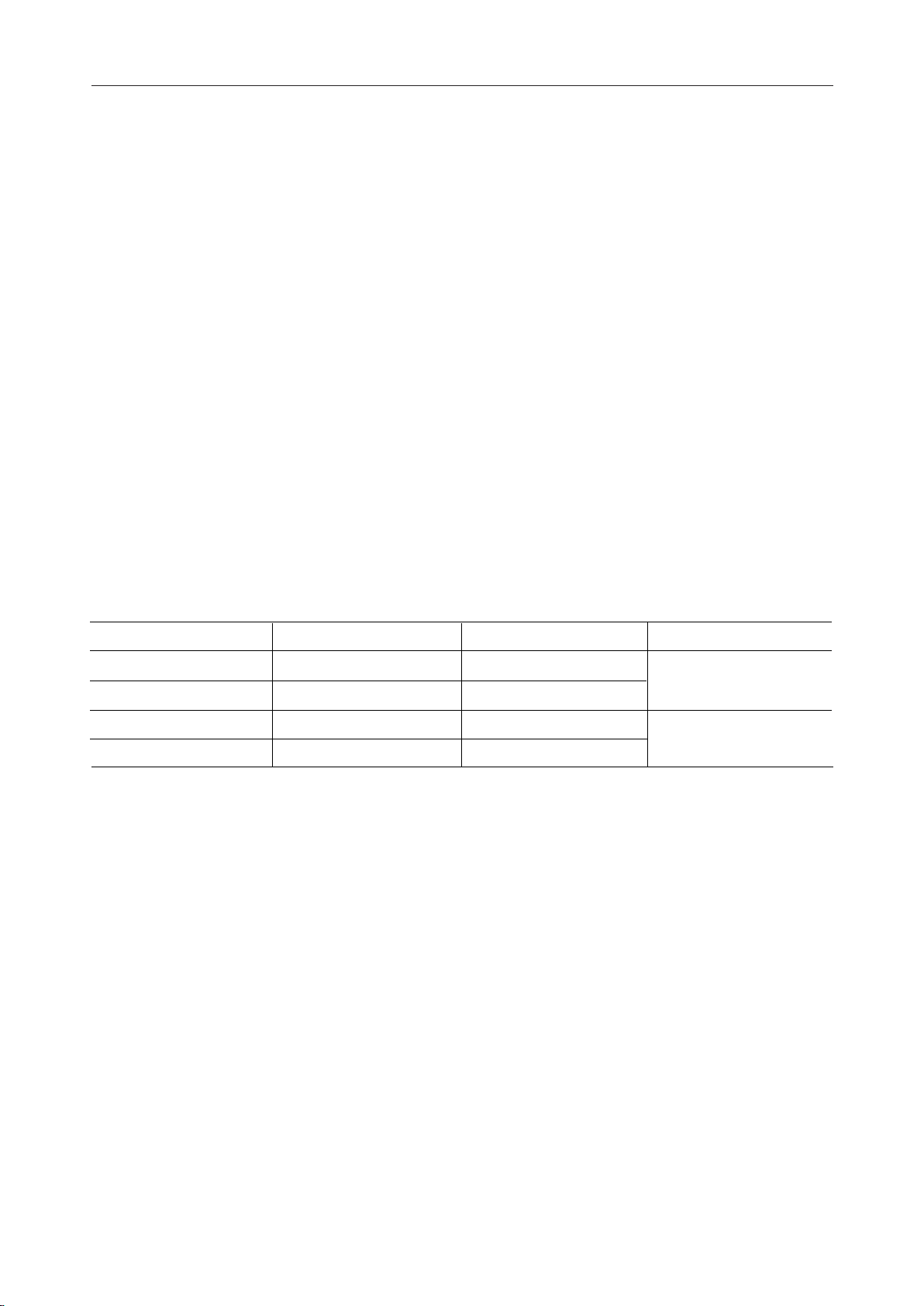
• Packageoptions:
44Pin 400mil plastic TSOP (Type II ) (TSOP II 44-P-400-0.80-K) (Product:MSM54V12222A-xxTS-K)
40Pin 400mil Plastic SOJ (SOJ40-P-400-1.27) (Product:MSM54V12222A-xxJS)
xx indicates speed rank.
PRODUCT FAMILIES
Family Access Time (Max.) Cycle Time (Min.) Package
MSM54V12222A-30-TS-K
MSM54V12222A-40-TS-K
MSM54V12222A-30JS 30 ns30 ns
MSM54V12222A-40JS 40 ns35 ns
30 ns30 ns
400 mil 44-pin TSOP (II)
40 ns35 ns
400 mil 40-pin SOJ
2
Page 3
OKI Semiconductor
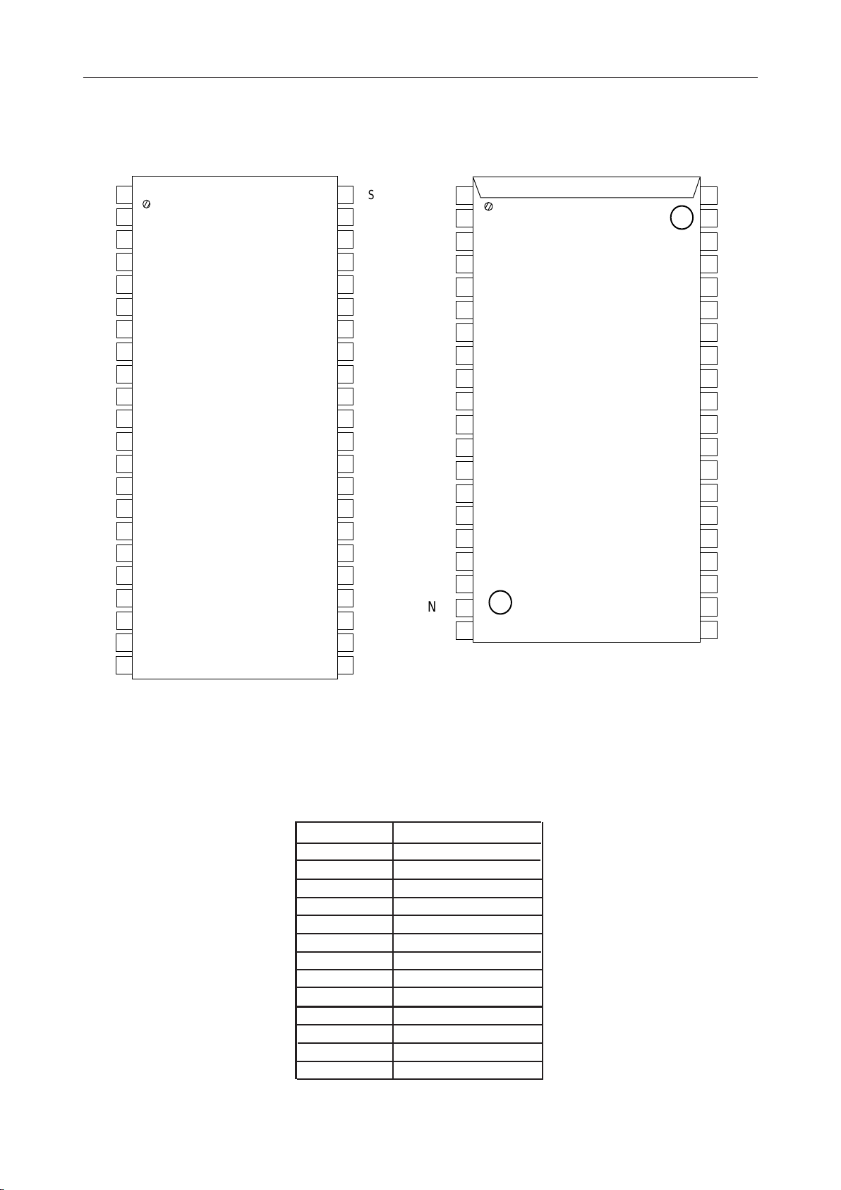
PIN CONFIGURATION (TOP VIEW)
V
SS
1
D
IN11
2
D
IN10
3
NC
4
DIN9
5
DIN8
6
DIN7
7
DIN6
8
NC
9
DIN5
10
11
IN
4
D
IN
3
D
12
DIN2
13
NC
14
DIN1
15
DIN0
16
SWCK
RSTW
NC
VWE
IE
V
CC
17
18
19
20
21
22
44
43
42
41
40
39
38
37
36
35
34
33
32
31
30
29
28
27
26
25
24
23
V
SS
D
OUT
D
OUT
NC
D
OUT
D
OUT
D
OUT
D
OUT
CC
V
D
OUT
D
OUT
OUT
D
D
OUT
V
SS
D
OUT
D
OUT
SRCK
RSTR
NC
RE
OE
V
CC
11
10
9
8
7
6
5
4
3
2
1
SWCK
0
RSTW
MSM54V12222A
V
SS
1
NC
2
D
IN
11
3
IN
10
D
D
D
D
D
4
D
IN
9
5
D
IN
8
6
IN
7
D
7
D
IN
6
8
D
IN
5
9
D
IN
4
10
IN
3
11
IN
2
12
IN
1
13
IN
0
14
15
16
WE
17
IE
18 23
NC
19
V
CC
20
40
39
38
37
36
35
34
33
32
31
30
29
28
27
26
25
24
22
21
V
SS
V
CC
D
OUT
OUT
D
D
OUT
D
OUT
OUT
D
D
OUT
D
OUT
D
OUT
D
OUT
OUT
D
D
OUT
D
OUT
SRCK
RSTW
RE
OE
V
SS
V
CC
11
10
9
8
7
6
5
4
3
2
1
0
44PIN Plastic TSOP (II)
(K Type)
Pin Name Function
SRCK Serial Read Clock
SWCK Serial Write Clock
WE Write Enable
RE Read Enable
IE Input Enable
OE Output Enable
RSTW Write Reset Clock
RSTR Read Reset Clock
Din0-11 Data Input
Dout0-11 Data Output
Vcc Power Supply(3.3V)
Vss Ground (0V)
NC No Connection
40PIn Plastick SOJ
3
Page 4
4
OKI Semiconductor
MSM54V12222A
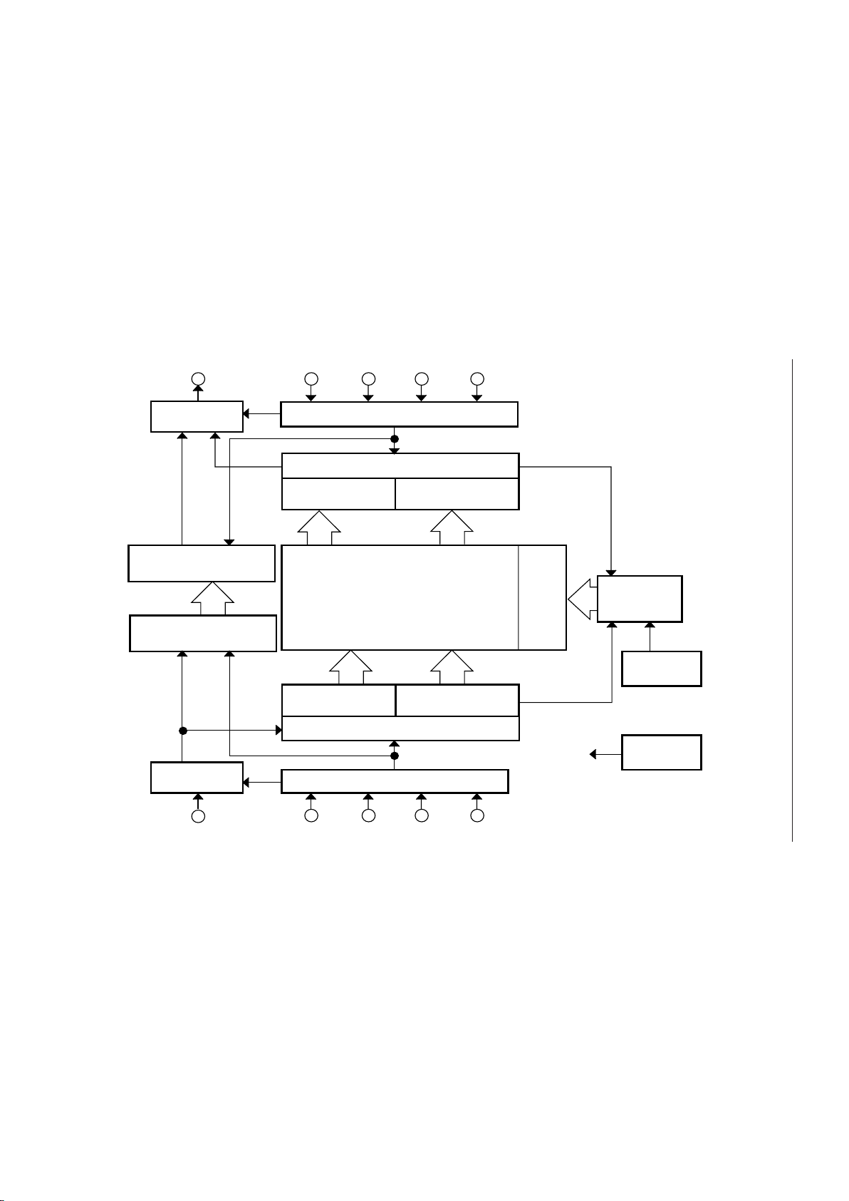
Dout (X12)
Data - out
Buffer (X12)
OE RE
RSTR SRCK
Serial Read Controller
512 Word Serial Read Register (X12)
Read line buffer
Low-Half (X12)
Read line buffer
High-Half (X12)
256 (X12)
256K (X12)
Memory
Array
X
Decoder
71Words
Sub-Register (X12)
Read/Write
and Refresh
Controller
Clock
Oscillator
Write line buffer
Low-Half (X12)
Write line Buffer
High-Half (X12)
512 Word Serial Write Register (X12)
Data-in
Buffer (X12)
Din (X12)
Serial Read Controller
IE WE RSTW
SWCK
71 Words
Sub-Register (X12)
256 (X12)
256 (X12) 256 (X12)
VBB
Generator
BLOCK DIAGRAM
Page 5

OKI Semiconductor
OPERATION
Write Operation
The write operation is controlled by tree clocks, SWCK, RSTW, and WE. Write operation is accomplished
by cycling SWCK and holding WE high after write address pointer reset operation or RSTW.
Each write operation, which begins after RSTW, must contain at least 80 active write cycles, i.e. SWCK
cycles while WE is high. To transfer the last data, which at that time are stored in the serial data registers
attached to DRAM array, to the DRAM array, an RSTW operation is required after the last SWCK cycle.
Note that every write timing of MSM54V12222A is delayed by one clock compared wih read timings for
easy cascading without any interface delay devices.
Write Reset : RSTW
The first positive transition of SWCK after RSTW going high resets the write address counters to zero.
RSTW setup and hold times are referenced to the rising edge of SWCK. Because the write reset function
is solely controlled by SWCK rising edge after high level of RSTW, the states of WE and IE are don't care
in the write reset cycle.
MSM54V12222A
Before RSTW may be brought high again for a further reset operation, it must have been low for at least
two SWCK cycles.
Data Inputs : Din0-11
Write Clock : SWCK
The SWCK latches the input data on chip when WE is high and also increments the internal write address
pointer. Data-in setup time, tDS and hold time, tDH, are referenced to the rising edge of SWCK.
Write Enable : WE
WE is used for data write enable/disable control. WE high level enables the input, and WE low level
disables the input and holds the internal write address pointer. There are no WE disable time (low) and
WE enable time (high) restrictions because MSM54V12222A is fully static operation as long as power is
on. Note that WE setup and hold times are referenced to the rising edge of SWCK.
Input Enable : IE
IE is used to enable/disable writing into memory. IE high level enables writing. The internal write address
pointer is always incremented by cycling SWCK regardless of IE level. Note that IE setup and hold times
are referenced to the rising edge of SWCK.
5
Page 6

MSM54V12222A
OKI Semiconductor
Read Operation
The read operation is controlled by tree clocks, SRCK, RSTR, and RE. Read operation is accomplished
by cycling SRCK and holding RE high after read address pointer reset operation or RSTR. Each read
operation, which begins after RSTR, must contain at least 80 active read cycles, i.e. SRCK cycles while
RE is high.
Read Reset : RSTR
The first positive transition of SRCK after RSTR going high resets the read address counters to zero.
RSTR setup and hold times are referenced to the rising edge of SRCK. Because the read reset function
is solely controlled by SRCK rising edge after high level of RSTR, the states of RE and RE are don't care
in the read reset cycle.
Before RSTR may be brought high again for a further reset operation, it must have been low for at least
*two SRCK cycles.
Data Out : Dout0-11
Read Clock : SRCK
Data is shifted out of the data registers triggered by the rising edge of SRCK when RE is high during a
read operation. The SRCK input increments the internal read address pointer when RE is high.
The three-state output buffer provides direct TTL compatibility ( no pullup resistor required). Data out is
the same polarity as data in. The output becomes valid after the access time interval tAC that begins with
the rising edge of SRCK. *There are no output valid time restriction on MSM54V12222A.
Read Enable : RE
The function of RE is gating of the SRCK clock, for incrementing the read pointer. When RE is high
before the rising edge of SRCK, the read pointer is incremented. When RE is low, the read pointer is not
incremented. RE setup times (tRENS and tRDSS) and RE hold times (tRENH and tRDSH) are referenced to the rising edge of the SRCK clock.
Output Enable : OE
OE is used to enable/disable the outputs. OE high level enables the outputs. The internal read address
pointer is always incremented by cycling SRCK regardless of OE level. Note that OE setup and hold times
are referenced to the rising edge of SRCK.
6
Page 7

OKI Semiconductor
MSM54V12222A
Power-up and Initialization
On Powering up, the device is designed to begin proper operation after at least 100 us after VCC has
stabilized to a value within the range of recommended operating conditions. After this 100 us stabilization
interval, the following initialization sequence must be performed.
Because the read and write address counters are not valid after power-up, a minimum of 80 dummy write
operations (SWCK cycles) and read operations (SRCK cycles) must be performed, followed by an RSTW
operation and an RSTR operation, to properly initialize the write and the read address pointer. Dummy
write cycles/RSTW and dummy read cycles/RSTR may occur simultaneously.
If these dummy read and write operations start while VCC and/or the substrate voltage have not stabilized, it is required to perform an RSTR operation plus a minimum of 80 SRCK cycles plus another RSTR
operation, and an RSTW operation plus a minimum of 80 SRCK cycles plus another RSTW operation to
properly initialize read and write address pointers.
Old/New Data Access
There must be minimum delay of 600 SWCK cycles between writing into memory and reading out from
memory if reading from the first field starts with an RSTR operation, before the start of writing the second
field, (before the next RSTW operation), then the data just written in will be read out.
The start of reading out the first field of data may be delayed past the beginning of writing in the second
field of data for as many as 70 SWCK cycles. If the RSTR operation for the first field read-out occurs less
than 70 SWCK cycles after the RSTW operation for the second field write-in, then the internal buffering of
the device assures that the first field will still be read out. The first field of data that is read out while the
second field of data is written is called "old data".
In order to read out "new data", i.e., the second field written in, the delay between an RSTW operation and
an RSTR operation must be at least 600 SRCK cycles. If the delay between RSTW and RSTR operations
is more than 71 but less than 600 cycles, then the data read out will be undetermined. It may be "old data"
or "new" data or a combination of old and new data. Such a timing should be avoided.
Cascade Operation
The MSM5412222A has been designed to allow easy cascading of multiple memory devices, in order to
obtain a higher storage depth or a longer delay than can be achieved with only one memory device.
7
Page 8

MSM54V12222A
ELECTRICAL CHARACTERISTICS
- Absolute Maximum Rating
OKI Semiconductor
Parameter Symbol
Input Output Voltage
Output Current
Power Dissipation
Operating Temperature
Storage Temperature
V
T
I
OS
P
D
T
opr
T
stg
- Recommended /peration Condition
Parameter Symbol MIN Unit
Power Supply Voltage
Power Supply Voltage
Input High Voltage
Input Low Voltage
V
CC
V
SS
V
IH
V
IL
- DC Characteristics
Parameter Symbol Condition Unit
Input Leakage Current
Output Leakage Current
Output "H" Level Voltage
Output "L" Level Voltage
Operating Current
Standby Current
I
I
V
V
I
CC1
I
CC2
LI
LO
OH
OL
Conditions
at Ta = 25°C, Vss
Ta = 25°C
Ta = 25°C
—
—
TYP MAX
3.0
0
2.4
–0.3
3.3
0
Vcc
0
0<Vi<+0.3,Other Pins Tested at V=0V
0<Vo<Vcc
IOH=-1mA
OL
=2mA
I
Minimum Cycle Time,Output Open
Input Pin=V
IH/VIL
Rating
–1.0~4.6
50
0~70
–55~150
3.6
0
Vcc+0.3
0.8
Min Max
-10
-10
2.4
Unit
V
mA
1
W
°C
°C
V
V
V
V
10
10
mA
mA
V
0.4
60
3
V
mA
mA
- Capacitance
Parameter
Input Capacitance (Din, SWCK, SRCK, RSTW, RSTR, WE, RE, IE, OE)
Output Capacitance (Dout)
Symbol MAX
Ci
Co
8
(Ta = 25°C, f = 1 MHz)
Unit
7
10
pF
pF
Page 9

OKI Semiconductor
AC CHARACTERISTICS
MSM54V12222A
(Vcc = 3.3V±0.3V, Ta = 0~70°C)
Parameter
Access Time from SRCK
Dout Hold Time from SRCK
Dout Enable Time from SRCK
SWCK "H" Pulse Width
SWCK "L" Pulse Width
Input Data Setup Time
Input Data Hold Time
WE Enable Setup Time
WE Enable Hold Time
WE Disable Setup Time
WE Disable Hold Time
IE Enable Setup Time
IE Enable Hold Time
IE Disable Setup Time
IE Disable Hold Time
WE "H" Pulse Width
WE "L" Pulse Width
IE "H" Pulse Width
IE "L" Pulse Width
RSTW Setup Time
RSTW Hold Time
SRCK "H" Pulse Width
SRCK "L" Pulse Width
RE Enable Setup Time
RE Enable Hold Time
RE Disable Setup Time
RE Disable Hold Time
OE Enable Setup Time
OE Enable Hold Time
OE Disable Setup Time
OE Disable Hold Time
RE "H" Puls Width
RE "L" Puls Width
OE "H" Puls Width
OE "L" Puls Width
RSTR Setup Time
RSTR Hold Time
SWCK Cycle Time
SRCK Cycle Time
Trandition Time (Rise and Fall)
Symbol
t
AC
t
DDCK
t
DECK
t
WSWH
t
WSWL
t
DS
t
DH
t
WENS
t
WENH
t
WDSS
t
WDSH
t
IENS
t
IENH
t
IDSS
t
IDSH
t
WWEH
t
WWEL
t
WIEH
t
WIEL
t
RSTWS
t
RSTWH
t
WSRH
t
WSRL
t
RENS
t
RENH
t
RDSS
t
RDSH
t
OENS
t
OENH
t
ODSS
t
ODSH
t
WREH
t
WREL
t
WOEH
t
WOEL
t
RSTRS
t
RSTRH
t
SWC
t
SRC
t
T
MSM54V12222A-30
MIN
—
6
6
12
12
5
6
0
5
0
5
0
5
0
5
10
10
10
10
0
10
12
12
0
5
0
5
0
5
0
5
10
10
10
10
0
10
30
30
3
MAX
30
—
30
—
—
—
—
—
—
—
—
—
—
—
—
—
—
—
—
—
—
—
—
—
—
—
—
—
—
—
—
—
—
—
—
—
—
—
—
30
MSM54V12222A-40
MIN
—
6
6
17
17
5
6
0
5
0
5
0
5
0
5
10
10
10
10
0
10
17
17
0
5
0
5
0
5
0
5
10
10
10
10
0
10
40
40
3
MAX
35
—
35
—
—
—
—
—
—
—
—
—
—
—
—
—
—
—
—
—
—
—
—
—
—
—
—
—
—
—
—
—
—
—
—
—
—
—
—
30
Unit
ns
ns
ns
ns
ns
ns
ns
ns
ns
ns
ns
ns
ns
ns
ns
ns
ns
ns
ns
ns
ns
ns
ns
ns
ns
ns
ns
ns
ns
ns
ns
ns
ns
ns
ns
ns
ns
ns
ns
ns
9
Page 10

MSM54V12222A
OKI Semiconductor
NOTE
1. Input signal reference levels for the parameter measurement are VIH=3.0V and VIL=0V.
The transition time tT is defined to be a transition time that signal transfers between VIH=3.0V
and VIL=0V.
2. AC measurements assume tT=3ns.
3. Read address must have more than 600 address delay than write address in every cycle
when asynchronous read/write is performed.
4. Read must have more than 600 address delay than write in order to read the data written in a
current series of write cycle which has been started last write reset cycle : this is called "new
data read".
When read has less than 70 address delay than write, the read data are the data written in a
previous series of write cycle which had been written before last write reset cycle: this is called
"old data read".
5. When the read address delay is between more than 71 and less than 599, read data will be
undetermined. However, normal write is achieved in this address condition.
6. Outputs are measured with a load equivalent to 1 TTL load and 30pF.
Output reference levels are VOH=2.0V and VOL=0.8V.
10
Page 11

OKI Semiconductor
WRITE CYCLE TIMING (Write Reset)
MSM54V12222A
SWCK
RSTW
Din
WE
IE
n cycle 0 cycle 1 cycle
t
t
T
t
DH
t
DS
n - 1 n
RSTWS
t
RSTWH
2 cycle
t
WSWHtWSWL
t
SWC
012
—V
—V
—V
—V
—V
—V
—V
—V
—V
—V
IH
IL
IH
IL
IH
IL
IH
IL
IH
IL
WRITE CYCLE TIMING (Write Enable)
n cycle disable cycle disable cycle n+1 cycle
SWCK
t
WDSH WDSS
t
WWEH
WE
Din
IE
RSTW
t
WENH
t
WWEL
n - 1 n
—V
IH
—V
IL
t
t
WENS
n+1
—V
—V
—V
—V
—V
—V
—V
—V
IH
IL
IH
IL
IH
IL
IH
IL
11
Page 12

MSM54V12222A
,
WRITE CYCLE TIMING (Input Enable)
n cycle n+1 cycle n+2 cycle n+3 cycle
SWCK
OKI Semiconductor
—V
IH
—V
IL
t
IENH
t
IE
t
Din
t
WIEL
n - 1 n
WE
RSTW
READ CYCLE TIMING (Read Reset)
IDSH
WIEH
t
IDSS
t
IENS
—V
IH
—V
IL
—V
n+3
—V
—V
—V
—V
—V
IH
IL
IH
IL
IH
IL
SRCK
RSTR
Dout
RE
OE
n cycle 0 cycle 1 cycle
t
t
T
RSTRS
t
AC
n - 1 n
t
RSTRH
2 cycle
t
WSRH
t
t
SRC
DDCK
t
WSRL
012
—V
—V
—V
—V
—V
—V
—V
—V
—V
—V
IH
IL
IH
IL
OH
OL
IH
IL
IH
IL
12
Page 13

OKI Semiconductor
,
,
READ CYCLE TIMING (Read Enable)
n cycle disable cycle disable cycle n+1 cycle
SRCK
MSM54V12222A
—V
IH
—V
IL
t
RENH
t
RDSH
RE
t
WREH
Dout
t
WREL
n - 1 n
OE
RSTR
READ CYCLE TIMING (Output Enable)
t
RDSS RENS
t
n+1
—V
—V
—V
—V
—V
—V
—V
—V
IH
IL
OH
OL
IH
IL
IH
IL
SRCK
OE
Dout
RE
RSTR
n cycle n+1 cycle n+2 cycle n+3 cycle
t
OENH
t
WOEN
n - 1 n
t
ODSH
t
WOEH
Hi-Z
t
ODSS OENS
t
t
DECK
n+3
—V
—V
—V
—V
—V
—V
—V
—V
—V
—V
IH
IL
IH
IL
OH
OL
IH
IL
IH
IL
13
Page 14

MSM54V12222A
NOTICENOTICE
NOTICE
NOTICENOTICE
1. The information contained herein is just a technical information for readers to know preliminary OKI
256KX12 bits FRAM idea.
2. The information herein does not guarantee configuration, features, characteristic, performance and
packages of the final products.
3. NO RESPONSIBILITY IS ASSUMED BY US FOR ANY CONSEQUENCE RESULTING FROM THE3. NO RESPONSIBILITY IS ASSUMED BY US FOR ANY CONSEQUENCE RESULTING FROM THE
3. NO RESPONSIBILITY IS ASSUMED BY US FOR ANY CONSEQUENCE RESULTING FROM THE
3. NO RESPONSIBILITY IS ASSUMED BY US FOR ANY CONSEQUENCE RESULTING FROM THE3. NO RESPONSIBILITY IS ASSUMED BY US FOR ANY CONSEQUENCE RESULTING FROM THE
INFORMATION HEREIN.INFORMATION HEREIN.
INFORMATION HEREIN.
INFORMATION HEREIN.INFORMATION HEREIN.
4. No part of the contents contained herein may be reprinted or reproduced without our prior permission.
OKI Semiconductor
Copyright 1994 OKI ELECTRIC INDUSTRY CO.,LTD
14
 Loading...