

Page 1

E2L0035-17-Y1
¡ Semiconductor MSM548333
¡ Semiconductor
This version: Jan. 1998
Previous version: Dec. 1996
MSM548333
240,384-Word ¥ 8-bit + 240,384-Word ¥ 4-bit Triple Port type Field Memory
DESCRIPTION
The MSM548333 is a high performance double triple-port type 2.88-Mbit, 768 bits ¥ 313 lines ¥ (8 +
4), Field Memory for Y-C separation signal control. The MSM548333 has two memory plain blocks:
Y area has 8 plains and C area has 4 plains. Each plain contains 768 ¥ 313 bits. Each plain has one input
port and two output ports. Access is done line by line. The line address must be set each time a line
is changed.
The MSM548333 is especially designed for high performance digital cameras, TVs, VTRs and Multimedia applications which require special operations such as time-base correction, noise reduction
and other digital techniques.
The MSM548333 is not designed for high end use in such applications as medical systems,
professional graphics systems which require long term picture storage, data storage systems and
others.
More than two MSM548333s can be cascaded directly without any delay devices between them.
Cascading MSM548333s provides larger capacity and longer delay.
X and Y serial address input enables random initial address setting of serial access in a page. Other
than the random address setting, MSM548333 has several types of address set modes such as line
hold, address jump to initial address and line increment. For example, address jump to initial X
address and line increment enable block access.
Self refresh function releases the MSM548333 from being applied external refresh control clocks even
though it contains dynamic type memory cells. Input enable control or IE pin enables write mask
function.
FEATURES
• Configuration
6-port configuration
Y area: 768 ¥ 313 ¥ 8-bit configuration ¥ 1 (serial write port)
768 ¥ 313 ¥ 8-bit configuration ¥ 2 (serial read port)
C area: 768 ¥ 313 ¥ 4-bit configuration ¥ 1 (serial write port)
768 ¥ 313 ¥ 4-bit configuration ¥ 2 (serial read port)
• Line by line access.
• X and Y serial address inputs for random serial initial bit address
• Asynchronous operation
• Serial read and write cycle times
Read cycle: 30 ns min.
Write cycle: 50 ns min.
• Low operating supply voltage: 3.3 V ±0.3 V
• Self-refresh.
• Various address reset mode for picture processing
• Write mask by IE.
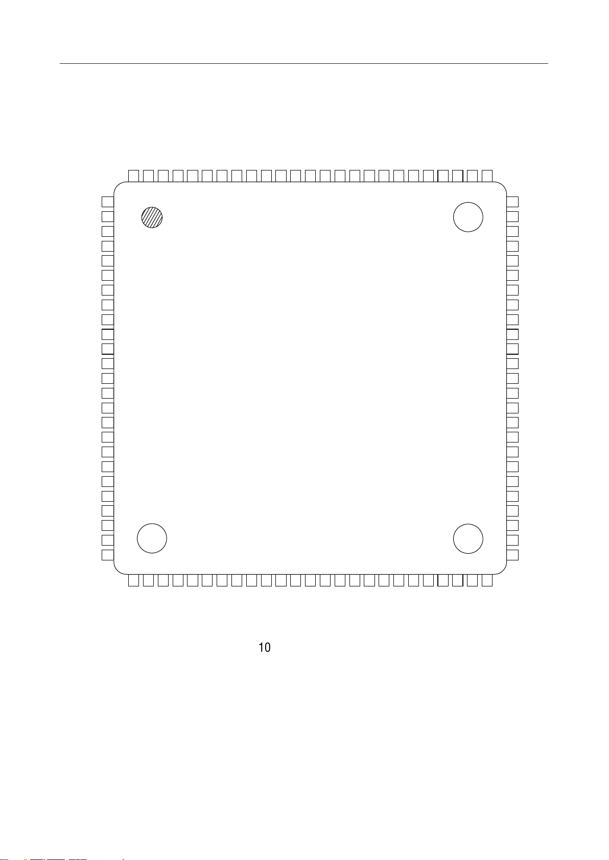
• Package:
100-pin plastic TQFP (TQFP100-P-1414-0.50-K) (Product : MSM548333TS-K)
1/42
Page 2
¡ Semiconductor MSM548333
PIN CONFIGURATION (TOP VIEW)
CCVCC
RR2/TR
REC2/RY
RCLKC2
NC
REY2/RY
RCLKY2
RADE1/RX
RXINC1
NC
RR1/TR
RE1/RY
NC
RCLK
NC
V
V
V
DOY1/0
DOY1/1
DOY1/2
DOY1/3
NC
V
DOY1/4
DOY1/5
RXINC2
RADE2/RX
99
98
TEST
97
96
RYAD1NCRXAD2
95
NC
100
1
7
8
9
10
11
12
13
14
15
SS
16
SS
17
SS
18
19
20
21
22
23
CC
24
25
94
93
RYADY2
RYADC2
92
91
NC
WXAD
89
90
RXAD1
WYADIEWE/WYNCWR/TR
87
86
WCLK
85
84
V
88
83
82
81
WADE/RX
WXINC
80
79
DINY/0
DINY/1
78
77
NC
76
75
742
733
724
715
706
69
68
67
66
65
64
63
62
61
60
59
58
57
56
55
54
53
52
51
DINY/2
DINY/3
DINY/4
NC
DINY/5
DINY/6
DINY/7
DINC/0
NC
DINC/1
DINC/2
NC
DINC/3
V
CC
V
SS
NC
V
SS
DOC2/0
DOC2/1
DOC2/2
NC
DOC2/3
V
CC
DOC1/0
DOC1/1
26
NC
27
28
DOY1/6
DOY1/7
29
SSVSS
V
30
31
32
DOY2/0
DOY2/1
33
34
35
37
36
CCVCCVCC
V
38
DOY2/2NCDOY2/3
100-Pin Plastic TQFP
39
NC
40
V
CC
41
42
43
44
DOY2/4NCDOY2/5
DOY2/6
46
45
SSVSS
V
DOY2/7
47
48
49
DOC1/3
DOC1/2
50
NC
2/42
Page 3

¡ Semiconductor MSM548333
Pin No. Pin Name Pin No. Pin Name Pin No. Pin Name Pin No. Pin Name
1 RR2/TR 26 NC 51 DOC1/1 76
CC
SS
SS
54 DOC2/3 79
55
NC
DOC2/2
7 RADE1/RX 32 DOY2/1 57
8 RXINC1 33 DOY2/2 58 83
9NC34NC59V
DOC2/1
DOC2/0
SS
78
80
81
82
84
10 RR1/TR 35 DOY2/3 60 NC 85
11 RE1/RY 36 V
12 NC 37 V
13 RCLK 38 V
CC
CC
CC
61 V
62 V
SS
CC
86
87 V
63 DINC/3 88 V
14 NC 39 NC 64 NC 89 NC
15 V
16 V
17 V
SS
SS
SS
40 V
CC
65 DINC/2 90 WXAD
41 DOY2/4 66 DINC/1 91 RYADC2
42 NC 67 NC 92 RYADY2
18 DOY1/0 43 DOY2/5 68 DINC/0 93 RXAD2
19 DOY1/1 44 DOY2/6 69 DINY/7 94 NC
20 DOY1/2 45 DOY2/7 70 DINY/6 95 RYAD1
21 DOY1/3 46 V
22 NC 47 V
23 V
CC
48 DOC1/3 73 DINY/4 98 RADE2/RX
SS
SS
71 DINY/5 96 RXAD1
72 NC 97 TEST
24 DOY1/4 49 DOC1/2 74 DINY/3 99 RXINC2
25 DOY1/5 50 NC 75 DINY/2 100 NC
NC
DINY/12 REC2/RY 27 DOY1/6 52 DOC1/0 77
DINY/03 RCLKC2 28 DOY1/7 53 V
WADE/RX4NC29V
WXINC5 REY2/RY 30 V
WR/TR6 RCLKY2 31 DOY2/0 56
NC
WE/WY
IE
WCLK
WYAD
CC
CC
3/42
Page 4

¡ Semiconductor MSM548333
Pin Name
Function
Serial Read/Write CycleAddress Setting Cycle
RCLK
Y1 and C1 Read Ports, Serial Read ClockY1, C1, Y2 and C2 Read Ports
X and Y Serial Address Strobes
RE1/RY Y1 and C1 Read Ports, Read EnableY1 and C1 Read Ports, Y Address Reset
DOY1/0 - 7 Y1 Read Port, Data Output—
DOC1/0 - 3 C1 Read Port, Data Output—
RR1/TR —Y1 and C1 Read Ports, Address Reset Mode Enable
RXINC1 —Y1 and C1 Read Ports, X Address Increment
RADE1/RX —
Y1 and C1 Read Ports, X and Y Address Input Enable
Y1 and C1 Read Ports, X Address Reset
RXAD1 —Y1 and C1 Read Ports, X Serial Address Data
RYAD1 —Y1 and C1 Read Ports, Y Serial Address Data
RR2/TR —Y2 and C2 Read Ports, Address Reset Mode Enable
RXINC2 —Y2 and C2 Read Ports, X Address Increment
RADE2/RX —
Y2 and C2 Read Ports, X and Y Address Input Enable
Y2 and C2 Read Ports, X Address Reset
RXAD2 —Y2 and C2 Read Ports, X Serial Address Data
RYADY2 —Y2 Read Port, Y Serial Address Data
RCLKY2 Y2 Read Port, Serial Read Clock—
REY2/RY
Y2 Read Port, Read EnableY2 Read Port, Y Address Reset
DOY2/0 - 7 Y2 Read Port, Data Output—
RYADC2 —C2 Read Port, Y Serial Address Data
RCLKC2
C2 Read Port, Serial Read Clock—
REC2/RY C2 Read Port, Read EnableC2 Read Port, Y Address Reset
DOC2/0 - 3 C2 Read Port, Data Output—
WCLK Y and C Write Ports, Serial Write ClockY and C Write Ports, X and Y Serial Address Strobes
WE/WY Y and C Write Ports, Write EnableY and C Write Ports, Y Address Reset
DINY/0 - 7 Y Write Port, Input Data
DINC/0 - 3 C Write Port, Input Data
—
WR/TR Y and C Write Ports, Write Data Transfer Y and C Write Ports, Address Reset Mode Enable
WXINC —Y and C Write Ports, X Address Increment
WADE/RX —
Y and C Write Ports, X and Y Address Input Enable
Y and C Write Ports, X Address Reset
WXAD —Y and C Write Ports, X Serial Address Data
WYAD —Y and C Write Ports, Y Serial Address Data
IE Input Enable—
V
CC
V
SS
Power Supply Voltage (3.3 V)
Ground (0 V)
TEST Connect to Power Supply Voltage (3.3 V)
Notes: 1. Same power supply voltage level must be provided to every VCC pin.
Same ground voltage level must be provided to every VSS pin.
2. Connect the TEST pin to the power supply.
3. NC must be opened. Don't connect to anything electrically.
4/42
Page 5
¡ Semiconductor MSM548333
5/42
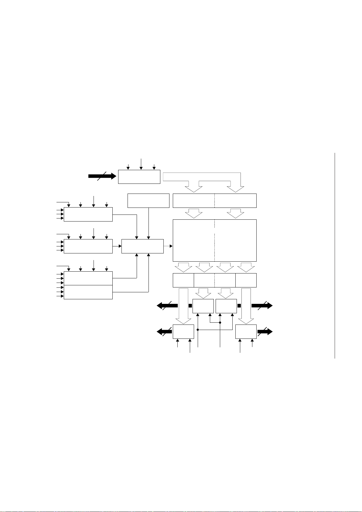
BLOCK DIAGRAM
WCLK
WE/WY
WYAD
WADE/RX
Write Address Control
WR/TR
WXINC
WXAD
RCLK
RE1/RY
RYAD1
RADE1/RX
Read Address Control
iY1/C1 j
RR1/TR
RXINC1
RXAD1
RCLK
REY2/RY
RYADY2
RADE2/RX
Read Address Control
iY2 j
RR2/TR
RXINC2
RXAD2
RCLK
REC2/RY
RYADC2
Read Address Control
iC2 j
Memory Controller
Refresh Controller
Write Buffer
WE/WY
WCLK
IE
12
DINY/0 to DINY/7
DINC/0 to DINC/3
Write Register
iY j
Write Register
iC j
Y-Region
768 ¥ 313 ¥ 8 bits
C-Region
768 ¥ 313 ¥ 4 bits
Memory Cell Array
Read
Register
iY2 j
4
DOC2/0 to DOC2/3
Read
Register
iY1 j
Read
Register
iC1 j
Read
Register
iC2 j
D
OUT
Buffer-1
8 bits
D
OUT
Buffer-1
4 bits
D
OUT
Buffer-2
8 bits
D
OUT
Buffer-2
4 bits
RCLKY2
REY2/RY
RE1/RY RCLK
REC2/RY
RCLKC2
4
DOC1/0 to DOC1/3
8
DOY2/0 to DOY2/7
8
DOY1/0 to DOY1/7
Page 6

¡ Semiconductor MSM548333
PIN FUNCTION (Note : Y1 = "port-1 of Y area", Y2 = "port-2 of Y area", C1 = "port-1 of C area",
C2 = "port-2 of C area "
READ RELATED
RCLK : Read Clock for Y1 and C1, Common Read Address Strobe Clock
RCLK is the read control clock input for Y1 and C 1. Synchronized with RCLK's rising edge, serial
read access from Y1 and C1 is executed when RE1/RY is high. (Note that the write port has one port,
Y and C, but the read port has dual ports, Y1 and C1 plus Y2 and C2. Y1 and C1 are controlled by the
common read clock RCLK. But Y2 and C2 are controlled by separated read clocks, RCLKY2 and
RCLKC2, asynchronously.)
The internal counter for the serial read address is incremented automatically on the rising edge of
RCLK. In a read address set cycle, all the read address bits which were input from each RXAD1, RYAD1,
RXAD2, RYADY2, and RYADC2 pins are stored into internal address registers synchronized
with RCLK. In this address set cycle, RADE1/RX and RADE2/RX must be held high and the RR1/
TR and RR2/TR must be held low.
In the read address reset cycle, various read address reset modes can be set synchronously with
RCLK. These reset cycles work to replace complicated serial address control which requires many
RCLK clocks with a simple reset cycle control requiring only a single RCLK cycle. It greatly facilitates
memory access.
RE1/RY : Read Enable for Y1 and C1/Read Y Address Reset Logic Function
RE1/RY is a dual function control input. RE1, one of the two functions of RE1/RY, is read enable.
RE1 enables or disables both internal read address pointers and data-out buffers of Y1 and C1. When
RE1/RY is high, the internal read address pointer for Y1 and C1 is incremented synchronously with
RCLK. When RE1/RY is low, even if the RCLK is input, the internal read address pointer is not
incremented.
RY, the second function of RE1/RY, performs a function for setting the read Y address (or bit address
in a certain line) reset mode in Y1 and C1. In a read address reset mode cycle, as defined by RR1/TR
being high, RY works as one of inputs which form several read reset logic as shown in the
"FUNCTION TABLE for read". In the address reset cycle, when RE1/RY level is low, each Y1and C1
internal read Y address is reset to 0. When RE1/RY is high, each Y1 and C1 internal read Y address
is reset to the respective address which was set in the previous read address set cycle.
DOY1/0-7 : Data-Outs for Y1
DOY1/0-7 are serial data-outs for Y1. Each corresponding data out buffer' impedance is controlled
by RE1/RY.
DOC1/0-3 : Data-Outs for C1
DOC1/0-3 are serial data-outs for C1. Each corresponding data out buffer' impedance is controlled
by RE1/RY.
RR1/TR : Read Reset for Y1 and C1
RR1/TR is a read reset control input for Y1 and C1. Read address reset modes are defined when RR1/
TR level is high according to the "FUNCTION TABLE for read".
RXINC1 : Read X Address Increment for Y1 and C1
RXINC1 is a read X address (or line address) increment control input for Y1 and C1. In the read
address reset cycle, defined by RR1/TR high, the common X address (or line address) for Y1 and C1
is incremented by RXINC1.
6/42
Page 7

¡ Semiconductor MSM548333
RADE1/RX : Read Address Enable for Y1 and C1/Read X Address Reset Logic Function
RADE1/RX is a dual function control input. RADE1, one of the two functions of RADE1/RX, is a read
address enable input for Y1 and C1. In the read address set cycle, defined by RR1/TR low, X address
(or line address) and Y address (or bit address in a certain line) input from the RXAD1 pin and RYAD1
pin are latched into internal read X address register and Y address register, respectively synchronously
with RCLK.
RX, the second function of RADE1/RX, works as an element to set read X address (or line address)
reset mode. In an address reset mode cycle, defined by RR1/TR level high, RX works as one of inputs
which form several read reset logic as shown in the "FUNCTION TABLE for read".
RXAD1 : Read X Address for Y1 and C1
RXAD1 is a read X address (or line address) input for Y1 and C1. RXAD1 specifies the line address.
9 bits of read X address data are input serially from RXAD1.
RYAD1 : Read Y Address for Y1 and C1
RYAD1 is a read Y address (or bit address in a certain line) input for Y1 and C1. RYAD1 specifies the
first bit address of consecutive serial read data in the line whose line address is defined by the X read
address from RXAD1. 10 bits of Y address data are input serially from RYAD1.
RR2/TR : Read Reset for Y2 and C2
RR2/TR is a read reset control input for Y2 and C2. Read address reset modes for Y2 and C2 are
defined when RR2/TR level is high based on the "FUNCTION TABLE for read".
RXINC2 : Read X Address Increment for Y2 and C2
RXINC2 is a read X address (or line address) increment control input for Y2 and C2. In the read
address reset cycle, defined by RR2/TR high, the common read X address (or line address) for Y2
and C2 is incremented by RXINC2.
RADE2/RX : Read Address Enable for Y2 and C2/Read X Address Reset Logic Function
RADE2/RX is a dual function control input. RADE2, one of the two functions of RADE2/RX, is a read
address enable input for Y2 and C2. In the read address set cycle, defined by RR2/TR high, the read
X address (or line address) and the read Y address (or bit address in a certain line), which are input
from the RXAD2, RYADY2 and RYADC2 pins, are latched into internal read X address register and
read Y address register, respectively, synchronously with RCLK.
RX, the second function of RADE2/RX, performs a function for setting the read X address (or line
address) reset mode. In a read address reset mode cycle, defined by RR2/TR level high, RX works
as one of inputs which form several read reset logic as shown in the "FUNCTION TABLE for read".
RXAD2 : Read X Address for Y2 and C2
RXAD2 is a read X address (or line address) input for Y2 and C2. RXAD2 specifies the line address.
9 bits of X address data is input serially from RXAD2.
RYADY2 : Read Y Address for Y2
RYADY2 is a read Y address (or bit address in a certain line) input for Y2. RYADY2 specifies the first
bit address of serial read data in the line whose line address is specified by the X address RXAD2.
10 bits of Y address data are input serially from RYADY2.
7/42
Page 8

¡ Semiconductor MSM548333
RCLKY2 : Read Clock for Y2
RCLKY2 is a read control clock input for Y2. (Note that there is RCLKC2 for C2.) Synchronized
with RCLKY2's rising edge, the serial read access from Y2 is executed when REY2/RY is high.
REY2/RY : Read Enable for Y2/Read Y Address Reset Logic Function for Y2
REY2/RY is a dual function control input. REY2, one of the two functions of REY2/RY, enables or
disables both internal read address pointers and data-out buffers of Y2. When REY2/RY is high, the
internal read address pointer for Y2 is incremented synchronously with RCLKY2. When REY2/RY
is low, even if RCLKY2 is input, the internal read address pointer is not incremented.
RY, the second function of REY2/RY, works as an element to set read Y address (or bit address in
a certain line) reset mode. In a read address reset mode cycle, defined by RR2/TR high, RY works
as one of inputs which form several read reset logic as shown in the "FUNCTION TABLE for read".
In the read address reset cycle, when REY2/RY is low, the internal read Y address for Y2 is reset to
0. When REY2/RY is high, the internal read Y address for Y2 is reset to the address which was set
in the previous address set cycle.
DOY2/0-7 : Data-Outs for Y2
DOY2/0-7 are serial data-outs for Y2. Each corresponding data-out-buffer' impedance is controlled
by REY2/RY.
RYADC2 : Read Y Address for C2
RYADC2 is a read Y address (or bit address in a certain line) input only for C2. RYADC2 specifies
the first bit address of serial read data in the line whose line address is specified by RXAD2. 10 bits
of Y address data are input serially from RYADC2.
RCLKC2 : Read Clock for C2
RCLKC2 is a read control clock input for only C2. (Note that there is RCLKY2 for Y2.) Synchronized
with RCLKC2, serial read access from C2 is executed when REC2/RY is high.
REC2/RY : Read Enable for C2/Read Y Address Reset Logic Function for C2
REC2/RY is a dual function control input. REC2, one of the two functions of REC2/RY, enables or
disables both internal read address pointers and data-out buffers for C2. When REC2/RY is high, the
internal read address pointer for C2 is incremented synchronously with RCLKC2. When REC2/RY
is low, even if RCLKC2 is input, the internal read address pointer is not incremented.
RY, the second function of REC2/RY, performs a function for setting the read Y address (or bit
address in a certain line) reset mode. In an address reset mode cycle, defined by RR2/TR high, RY
works as one of inputs which form several read reset logic as shown in the "FUNCTION TABLE for
read". In the read address reset cycle, when REC2/RY is low, the internal read Y address for C2 is
reset to 0. When REC2/RY is high, the internal read Y address for C2 is reset to the address which
was set in the previous read address set cycle.
DOC2/0-3 : Data-Outs for C2
DOC2/0-3 are serial data-outs for C2. Each corresponding data out buffer' impedance is controlled
by REC2/RY.
8/42
Page 9

¡ Semiconductor MSM548333
WRITE RELATED
WCLK : Write Clock for Y and C
WCLK is a write control clock input for Y and C ports. Synchronized with WCLK's rising edge, serial
write access into Y and C ports is executed when WE/WY is high and IE is high. (Note that the read
port is dual port, Y1 and C1 + Y2 and C2, but write port has only one port, Y + C. X8 of Y and X4 of
C inputs are controlled by a common WCLK, that is, in the write port, the MSM548333 is controlled
as a X12 FRAM.)
According to WCLK clocks, the internal counter for the serial address is incremented automatically.
In a write address set cycle, all the write addresses which were input from WXAD and WYAD are
stored into internal address registers synchronously with WCLK. In this address set cycle, WADE/
RX must be held high and WR/TR must be held low.
In the write address reset cycle, various write address reset modes can be set synchronously with
WCLK. These reset cycles replace complicated serial address control with simple reset cycle control
which requires only one WCLK cycle. It greatly facilitates memory access.
WE/WY : Write Enable for Y and C/Write Y Address Reset Logic Function
WE/WY is a dual function control input. WE, one of the two functions of WE/WY, is write enable.
WE enables or disables both internal write address pointers and data-in buffers of Y and C. When
WE/WY is high, the internal write address pointer for Y and C is incremented synchronously with
WCLK. When WE/WY is low, even if WCLK is input, the internal write address pointer is not
incremented.
WY, the second function of WE/WY, performs a function for setting the write Y address (or bit
address in a certain line) reset mode in Y and C. In a write address reset mode cycle, defined by WR/
TR high, WY works as one of inputs which form several write reset logic as shown in the "FUNCTION
TABLE for write". In the address reset cycle, when WE/WY level is low, each Y and C internal write
Y address is reset to 0. When WE/WY is high, each Y and C internal write Y address is reset to the
respective address which was set in the previous write address set cycle.
DINY/0-7 : Data-Ins for Y
DINY/0-7 are serial data-ins for Y. Each corresponding data-in-buffer is masked by IE.
DINC/0-3 : Data-Ins for C
DINC/0-3 are serial data-ins for C. Each corresponding data-in-buffer is masked by IE.
WR/TR : Write Reset for Y and C
WR/TR is a write reset control input for Y and C. Write address reset modes are defined when WR/
TR level is high according to the "FUNCTION TABLE for write".
WXINC : Write X Address Increment for Y and C
WXINC is a write X address (or line address) increment control input for Y and C. In the write address
reset cycle, defined by WR/TR high, the common write X address (or line address) for Y and C is
incremented by WXINC.
WADE/RX : Write Address Enable for Y and C/Write X Address Reset Logic Function
WADE/RX is a dual functional control input. WADE, one of the two functions of WADE/RX, is a
write address enable input for Y and C. In the write address reset cycle, defined by WR/TR high, X
address (or line address) and Y address (or bit address in a certain line) input from WXAD and
WYAD are latched into internal write X address register and Y address register.
9/42
Page 10

¡ Semiconductor MSM548333
WXAD : Write X Address for Y and C
WXAD is a write X address (or line address) input for Y and C. WXAD specifies line address. 9 bits
of write X address data are input serially from WXAD.
WYAD : Write Y Address for Y and C
WYAD is a read Y address (or bit address in a certain line) input for Y and C. WYAD specifies the
first bit address of consecutive serial write data in the line whose line address is defined by X write
address from WXAD. 10 bits of write Y address data are input serially from WYAD.
IE : Input Enable for Y and C
IE is an input enable which controls the write operation. When IE is high, the input operation is
enabled. When IE is low, the write operation is masked. When WE/WY signal is high, and IE low,
the internal serial write address pointer is incremented on the rising edge of WCLK without actual
write operations. This function facilitates picture in picture function in a TV system.
10/42
Page 11
¡ Semiconductor MSM548333
OPERATION MODE
Write
1. Write operation
Before the write operation begins, X address (or line address) and Y address (or bit address
in the line specified by the X address) must be input to set the initial bit address for the
following serial write access. When WE/WY and IE are high, a set of serial 12-bit -width write
data on DINY/0-7 and DINC/0-3 is written into write registers attached to the DRAM
memory arrays temporarily on the rising edge of WCLK.
Following 12-bit-width serial input data is written into the memory locations in the write
register designated by an internal write address pointer which is advanced by WCLK. This
enables continuous serial write on a line. When write clock WCLK and read clock RCLK are
tied together and are controlled by a common clock or CLK, more than two MSM548333s can
be cascaded directly without any delay devices between the MSM548333s because the read
timing is delayed by one CLK cycle to the write timing. When the write operation on a line is
terminated, be sure to perform a write transfer operation by WR/TR in order to store the
written data in the write registers to the corresponding memory cells in the DRAM memory
arrays.
2. Write address pointer increment operation
The write address pointer is incremented synchronously with WCLK when WE/WY is high.
When the write address pointer reaches the last address of a line, it stops at the last address
and no address increment occurs.
Relationship between the WE/WY and IE input levels,
Write Address pointer, and data input status
WCLK Rise
WE/WY
H
H
L
IE
H
L
—
Internal Write
Address Pointer
Incremented
Stopped
Data Input
Inputted
Not Inputted
When WE/WY and IE are high, the write operation is enabled.
If IE level goes low while WCLK is active, the write operation is halted but the write address
pointer will continue to advance. That is, IE enables a write mask function. When WE/WY
goes low, the write address pointer stops without WCLK.
Read (Here, "port-1 of Y area" is Y1, "port-2 of Y area" is Y2, "port-1 of C area" is C1, "port-2 of C area"
is C2.)
1. Read operation
MSM548333 has dual read ports, port-1 for Y and C memory areas and port-2 for Y and C
memory areas. Note that the read of Y1 and C1 are controlled by a common control clock at
the same time. But the read of Y2 and C2 are controlled by separate sets of control clocks,
independently.
Before the read operation begins, the X address (or line address) and Y address (or bit address
in the line specified by the X address) must be input for setting initial bit address for the
following serial read access.
When RE1/RY is high, a set of serial 12-bit-width read data on DOY1/0-7 pins and DOC1/
0-3 pins is read from read registers attached to DRAM memory arrays on the rising edge of
RCLK.
When REY2/RY is high, a set of serial 8-bit-width read data on DOY2/0-7 pins is read from
read registers attached to DRAM memory arrays on the rising edge of RCLKY2.
11/42
Page 12

¡ Semiconductor MSM548333
When REC2/RY is high, a set of 4-bit-width serial read data on DOC2/0-3 is read from the
read registers attached to DRAM memory arrays on the rising edge of RCLKC2.
Each access time is specified by the rising edges of RCLK, RCLKY2 and RCLKC2.
2. Read address pointer increment operation
There are three separate pointers for dual port serial read operation. The first one is the read
pointer for Y1 and C1 which is incremented by RCLK when RE1/RY is high. The second one
is the read pointer for Y2 which is incremented by RCLKY2 when REY2/RY is high. The third
one is the read pointer for C2 which incremented by RCLKC2 when REC2/RY is high. When
each read address pointer reaches the last address of a line, it stops at the last address and no
address increment occurs.
Initial Address Setting (Write/Read Independent)
Any read operations are prohibited in the read initial address set period. Similarly, any write
operations are prohibited in the write initial address set period. Note that read initial address set and
write initial address set can occur independently. Similarly, read access can be achieved independently
from write initial address set period and write access can be achieved independently from read initial
address set cycles.
1. Write address setting
During a write, MSM548333 has one write address enable input, WADE/RX. Note that there
are two read address enable inputs for read. WADE/RX enables Y and C initial read address
inputs. When WADE/RX is high, 9 bits of serial X address (or line address) for Y and C and
10 bits of serial Y address (or bit address in the line specified by the X address) for Y and C are
input in parallel from WXAD and WYAD respectively.
The operations above enable selection of specific lines randomly and enables the start of serial
write access synchronized with write clock WCLK. Address for each line must be input
between each line access. In other words, MSM548333's write is achieved in a "line by line"
manner. Any write operations are prohibited in the initial write address set periods.
Y and C Serial write input enable time t
must be kept for starting a serial write just after
SWE
the initial write address set period.
2. Read address setting
During a read, MSM548333 has two read address enable inputs, RADE1/RX and RADE2/RX.
RADE1/RX enables Y1 and C1 initial read address inputs. Similarly, RADE2/RX enables Y2
and C2 initial read address inputs.
When RADE1/RX is high, 9 bits of serial X address (or line address) for Y1 and C1 and 10 bits
of serial Y address (or bit address in the line specified by the X address) for Y1 and C1 are input
in parallel from RXAD1 and RYAD1, respectively. Note that the X and Y address inputs when
RADE1/RX is high are for Y1 and C1.
When RADE2/RX is high, 9 bits of serial X address (or line address) for Y2 and C2 is input from
RXAD2. In the same period, 10 bits of serial Y address (or bit address in the line specified by
the X address) for Y2 is input from RYADY2 pin and another 10 bits of serial Y address (or bit
address in the line specified by the same X address input from RXAD2) for C2 is input from
RYADC2 pin. Note that the X address input here is for both Y2 and C2 and the two sets of Y
address inputs from RYADY2 and RYADC2 are for Y2 and C2, respectively. That is,
MSM548333 can't set separate line addresses in Y2 and C2 but can set separate initial bit
address in Y2 and C2 on the specified lines by the common line address.
The operations above enable selection of specific lines randomly and enables the start of serial
read access synchronized with read clocks, RCLK for Y1 and C1, RCLKY2 for Y2 and RCLKC2
for C2. Address for each line must be input between each line access. In other words,
12/42
Page 13

¡ Semiconductor MSM548333
MSM548333's read operation is achieved in "line by line" manner.
Any read operations are prohibited in the initial read address set periods. Serial read
operations for Y1 and C1, and also Y2 and C2, are prohibited while RADE1/RX is high.
Similarly, serial read operations for Y1 and C1, and also Y2 and C2, are prohibited while
RADE2/RX level is high. Y1 and C1 Serial read port enable time t
enable time t
and C2 serial read port enable time t
SREY2
must be kept for starting a serial
SREC2
, Y2 serial read port
SRE1
read just after the initial read address set period.
Initial Address Reset Modes (Write/Read Independent)
The initial address reset modes replace complicated read or write initial address settings with simple
reset cycles. Initial address reset modes are selected by RR/TR high during read and WR/TR high
during write. As in normal read or write address settings, any read operations are prohibited in the
read address reset cycles. Similarly, any write operations are prohibited in the initial write address
reset cycles. Note that read initial address reset and write initial address reset can occur independently.
Similarly, read access can be achieved independently from write initial address reset cycles and write
access can be achieved independently from read initial address reset cycles.
Input addresses are stored into address registers which are connected with address counter which
controls address pointer operation. In the serial access operation, the input address into the address
registers are kept.
Serial write data input enable time t
port read enable time t
, C2 serial read port read enable time t
SREY2
, Y1 and C1 read port read enable time t
SWE
SREC2
, Y2 serial read
SRE1
must be kept for starting
serial read or write just after the initial read or write address reset cycles. Note that all the read ports'
initial address reset must occur with the same timing.
1. Original address reset No.1 - "X, Y address counter reset" By the "Original address reset No.1" logic which is composed by a combination of control
input' levels, the address counter is reset to (0,0), and then, the address pointer is initialized
to (0,0). Reference the "FUNCTION TABLE" for read and write shown later. After the reset
mode, serial access starts from the address (0,0) : the line address is "0" and the initial bit
address on the line is (0,0).
The address counter is reset by this reset mode but the address register, which stored input
address in the previous address reset cycle or address set cycle, is not reset. The non-initialized
address can be used as a preset address in "address jump reset" mode. When the address
register must be reset, choose "address register reset" mode.
2. Original address reset No.2 - "X,Y address register reset" By the "Original address reset No.2" logic, the address register is reset, and then, the address
counter and address pointer are initialized to address (0,0) automatically. After the reset
mode, serial access starts from the address (0,0) : the line address is "0" and the initial bit
address on the line is (0,0)
Both address register and address counter are reset to (0,0) and the stored initial address in the
previous address reset cycle or address set cycle is cleared by this "address register reset". Once
the reset mode is selected, the reset address (0,0) is stored in the address register as a preset
address until next initial address set or reset operation. The address can be used as a preset
address in the "address jump reset" mode.
Note that REY2/RY and REC2/C2 must be both "L" at the same time when the "address
register reset" is selected. REY2/RY = "L" and REC2/RY = "H" or REY2/RY = "H" and REC2/
RY = "L" are prohibited.
3. Original address reset No.3 - Y address counter reset" By the "Original address reset No.3" logic, the Y address register is reset, and then, address
13/42
Page 14

¡ Semiconductor MSM548333
pointer for the line access is initialized to Y address (0). The X address Xi which specifies a
certain line address is one which was stored in the X address register in the previous address
reset or address set cycle. After the reset mode, serial access starts from the address (Xi,0) : line
address is "Xi" and initial bit address on the line is (0).
The Y address counter is reset by this reset mode but the Y address register, which stored the
input initial Y address in the previous address reset cycle or address set cycle, is not reset. The
non-initialized Y address can be used as a preset Y address in the "address jump reset" mode.
4. Line increment reset No.1 - "X address counter increment and Y address counter reset" By the "Line increment reset No.1" logic, the X address counter is incremented by one from
the current X address and Y address is reset to address (0). That is, by the reset mode, serial
access from the Y = (0) on the next line is enabled.
5. Line increment reset No.2 - "X address counter increment reset and Y address counter
initialize" By the "Line increment reset No.2" logic, the X address counter is incremented by one from
the current X address and Y address is initialized to the Y address set in the previous address
set cycle. This enables block access on the screen.
6. Line hold reset No. 1 (1) operation
When a predetermined input level is set during the reset setting cycle, access is executed
starting from the first word on the current line.
7. Line hold (2) operation
When a predetermined input level is set during the reset setting cycle, access is executed
starting from the word address on the current line which is initialized.
8. Address jump operation
When a predetermined input level is set during the reset setting cycle, a jump may be caused
to the initialized line or word address.
In the case of a read, set the same level in the Y2 and C2 regions for this operation.
Note :During one reset setting cycle, a plurality of resets cannot be set.
14/42
Page 15

¡ Semiconductor MSM548333
Power ON
Power must be applied to RCLK, RCLKY2, RCLKC2, RE1/RY, REY2/RY, REC2/RY and WE/WY
input signals to pull them "Low" before or when the VCC supply is turned on.
After power-up, the device is designed to begin proper operation in at least 200 ms after VCC has
reached the specified voltage. After 200 ms, a minimum of one line dummy write operation and read
operation is required according to the address setting mode, because the read and write address
pointers are not valid after power-up.
New Data Read Access
In order to read out "new data', the delay between the beginning of a write address setting cycle and
read address setting cycle must be at least two lines.
Old Data Read Access
In order to read out "old data", the delay between the beginning of a write address setting cycle and
read address setting cycle must be more than 0 but less than a half line.
15/42
Page 16

¡ Semiconductor MSM548333
FUNCTION TABLE
1. Write
Mode No.
Address Reset
Mode
Address Setting
Mode
Description of
Operation
1 Write Transfer H L L L
2 Reset (1) H L L H
3 Reset (2) H H L H
4 Line Increment (1) H H L L
Line Increment (2)
5 HHHL
6 Reset (3) H L H H
7 Line Hold (2) H L H L
8 Address Jump HHHH
— First Address Setting L L L H
(Note)
WR/TR WXINC WE/WY
WADE/RXInternal Address
X and Y cleared
to (0, 0)
X and Y cleared
to (0, 0)
X set and Y cleared
to (Xn + 1, 0)
X and Y set
to (Xn +1, Yi)
X cleared and Y
set to (0, Yi)
X and Y set
to (Xn, Yi)
X and Y set
to (Xi, Yi)
X and Y set
Pointer
Note : When Address reset mode No. 3 is executed, the address X and Y which are set previously will
be cleared. For write, Line hold (1) is not provided.
16/42
Page 17

¡ Semiconductor MSM548333
2. Read
Mode No.
Address Reset
Mode
Address Setting
Mode
Description of
Operation
1 Line Hold (1) H L L L
2 Reset (1) H L L H
3 Reset (2) H H L H
4 Line Increment (1) H H L L
5 HHHL
Line Increment (2)
6 Reset (3) H L H H
7 Line Hold (2) H L H L
8 Address Jump HHHH
— First Address Setting L L L H
(Note)
RR*/TR RXINC* RE*/RY
RADE*
/RX
*
*
Internal Address
X set and Y cleared
to (Xn, 0)
X and Y cleared
to (0, 0)
X and Y cleared
to (0, 0)
X set and Y cleared
to (Xn + 1, 0)
X and Y set
to (Xn + 1, Yi)
X cleared and Y set
to (0, Yi)
X and Y set
to (Xn, Yi)
X and Y set
to (Xi, Yi)
X and Y set
Pointer
RR*/TR : RR1/TR, RR2/TR RXINC* : RXINC1, RXINC2
RE*/RY : RE1/RY, REY2/RY, REC2/RY RADE*/RX : RADE1/RX, RADE2/RX
* Set the same level in the Y2 and C2 regions.
Note : When address reset mode No. 3 is executed, the addresses X and Y which are set previously
will be cleared.
17/42
Page 18

¡ Semiconductor MSM548333
ELECTRICAL CHARACTERISTICS
Absolute Maximum Ratings
Parameter Symbol Condition Rating
Pin Voltage V
Short Circuit Output Current I
Power Dissipation P
Operating Temperature T
Storage Temperature
T
OS
D
opr
T
stg
Recommended Operating Conditions
Parameter Symbol Min.
Power Supply Voltage V
Power Supply Voltage V
"H" Input Voltage V
"L" Input Voltage V
CC
SS
IH
IL
Ta = 25°C, with respect to V
Ta = 25°C 50 mA
Ta = 25°C 1 W
— 0 to 70°C
— –55 to 150°C
Typ.
3.0
0
2.1
–0.5
3.3
V
0
CC
0
SS
Max.
V
CC
3.6
0
+ 0.3
0.8
–0.5 to 4.6 V
(Ta = 0 to 70°C)
Unit
V
V
V
V
DC Characteristics
Parameter Symbol Condition
"H" Output Voltage V
"L" Output Voltage V
Input Leakage Current I
Output Leakage Current I
Power Supply Current
(During Operation)
Power Supply Voltage
(During Standby)
Capacitance
Parameter Symbol
Input Capacitance C
Output Capacitance C
I
I
OH
OL
LI
LO
CC1
CC2
O
(V
= 3.0 to 3.6 V, Ta = 0 to 70°C)
CC
Unit
V
V
IOH = –0.1 mA
IOL = 0.1 mA
Min.
2.2
—
Max.
—
0.7
0 < VI < VCC + 1
–10
10
mA
Other input voltage 0 V
0 < VO < 3.6
–10
min. cycle — mA
Input pin = VIL/V
IH
—mA
10
50
10
mA
(Ta = 25°C, f = 1 MHz)
Max.
I
7
7
Unit
pF
pF
18/42
Page 19

¡ Semiconductor MSM548333
AC Characteristics (1/4)
= 3.3 V ±0.3 V, Ta = 0 to 70°C)
CC
Min.
50
Max.
—
Unit
—
—
—
—
—
—
—
—
—
—
—
—
—
—
—
—
—
—
—
—
—
—
—
—
—
—
—
—
—
—
—
—
—
—
—
—
—
—
ns
ns15t
ns15t
ns5t
ns7t
ns7t
ns7t
ns5t
ns7t
ns7t
ns7t
ns5t
ns7t
ns5t
ns7t
ns5000t
ns5t
ns7t
ns7t
ns7t
ns5t
ns7t
ns7t
ns7t
ns5t
ns15t
ns5t
ns7t
ns7t
ns7t
ns5t
ns7t
ns7t
ns7t
ns5t
ns7t
ns7t
ns7t
ns5t
Parameter
WCLK Cycle Time
WCLK "H" Pulse Width
WCLK "L" Pulse Width
Serial Write Address Input Active Setup Time
Serial Write Address Input Active Hold Time
Serial Write Address Input Inactive Hold Time
Serial Write Address Input Inactive Setup Time
Write Transfer Instruction Setup Time
Write Transfer Instruction Hold Time
Write Transfer Instruction Inactive Hold Time
Write Transfer Instruction Inactive Setup Time
Serial Write X Address Setup Time
Serial Write X Address Hold Time
Serial Write Y Address Setup Time
Serial Write Y Address Hold Time
Serial Write Data Input Enable Time
Write Instruction Setup Time
Write Instruction Hold Time
Write Instruction Inactive Hold Time
Write Instruction Inactive Setup Time
IE Enable Setup Time
IE Enable Hold Time
IE Disable Hold Time
IE Disable Setup Time
Input Data Setup Time
Input Data Hold Time
WR/TR-WCLK Active Setup Time
WR/TR-WCLK Active Hold Time
WR/TR-WCLK Inactive Hold Time
WR/TR-WCLK Inactive Setup Time
WXINC-WCLK Active Setup Time
WXINC-WCLK Active Hold Time
WXINC-WCLK Inactive Hold Time
WXINC-WCLK Inactive Setup Time
WADE/RX-WCLK Active Setup Time
WADE/RX-WCLK Active Hold Time
WADE/RX-WCLK Inactive Hold Time
WADE/RX-WCLK Inactive Setup Time
WE/WY-WCLK Active Setup Time
Measurement Conditions: (V
Symbol
t
WCLK
WWCLH
WWCLL
WAS
WAH
WADH
WADS
WTRS
WTRH
WTDH
WTDS
WXAS
WXAH
WYAS
WYAH
SWE
WES
WEH
WEDH
WEDS
IES
IEH
IEDS
IEDH
DS
DH
WRS
WRH
WRDH
WRDS
WINS
WINH
WINDH
WINDS
WRXS
WRXH
WRXDH
WRXDS
WRYS
19/42
Page 20

¡ Semiconductor MSM548333
AC Characteristics (2/4)
Measurement Conditions: (V
Parameter
WE/WY-WCLK Active Hold Time
WE/WY-WCLK Inactive Hold Time
WE/WY-WCLK Inactive Setup Time
RCLK Cycle Time
RCLK "H" Pulse Width
RCLK "L" Pulse Width
RR1/TR-RCLK Active Setup Time
RR1/TR-RCLK Active Hold Time
RR1/TR-RCLK Inactive Hold Time
RR1/TR-RCLK Inactive Setup Time
RXINC1-RCLK Active Setup Time
RXINC1-RCLK Active Hold Time
RXINC1-RCLK Inactive Hold Time
RXINC1-RCLK Inactive Setup Time
RADE1/RX-RCLK Active Setup Time
RADE1/RX-RCLK Active Hold Time
RADE1/RX-RCLK Inactive Hold Time
RADE1/RX-RCLK Inactive Setup Time
RE1/RY-RCLK Active Setup Time
RE1/RY-RCLK Active Hold Time
RE1/RY-RCLK Inactive Hold Time
RE1/RY-RCLK Inactive Setup Time
Y1 and C1 Read Port Output Instruction Setup Time
Y1 and C1 Read Port Output Instruction Hold Time
Y1 and C1 Read Port Output Instruction Inactive Hold Time
Y1 and C1 Read Port Output Instruction Inactive Setup Time
Y1 and C1 Read Port Read EnableTime
Y1 and C1 Read Port Read Data Hold Time
Y1 and C1 Output Access Time
Y1 and C1 Data Output Turn Off Delay Time
RR2/TR-RCLK Active Setup Time
RR2/TR-RCLK Active Hold Time
RR2/TR-RCLK Inactive Hold Time
RR2/TR-RCLK Inactive Setup Time
RXINC2-RCLK Active Setup Time
RXINC2-RCLK Active Hold Time
RXINC2-RCLK Inactive Hold Time
RXINC2-RCLK Inactive Setup Time
RADE2/RX-RCLK Active Setup Time
Symbol
t
WRYH
WRYDH
WRYDS
RCLK
WRCLH
WRCLL
RRS1
RRH1
RRDH1
RRDS1
RINS1
RINH1
RINDH1
RINDS1
RRXS1
RRXH1
RRXDH1
RRXDS1
RRYS1
RRYH1
RRYDH1
RRYDS1
RES1
t
REH1
REDH1
REDS1
SRE1
OH1
AC1
OHZ1
RRS2
RRH2
RRDH2
RRDS2
RINS2
RINH2
RINDH2
RINDS2
RRXS2
= 3.3 V ±0.3 V, Ta = 0 to 70°C)
CC
Min.
7
Max.
—
Unit
—
—
—
—
—
—
—
—
—
—
—
—
—
—
—
—
—
—
—
—
—
—
AC1
—
—
—
—
—
—
—
—
—
—
—
—
—
—
ns
ns7t
ns7t
ns30t
ns12t
ns12t
ns5t
ns7t
ns7t
ns7t
ns5t
ns7t
ns7t
ns7t
ns5t
ns7t
ns7t
ns7t
ns5t
ns7t
ns7t
ns7t
ns5t
nst
ns7t
ns7t
ns5000t
ns15t
ns30\t
ns—20t
ns5t
ns7t
ns7t
ns7t
ns5t
ns7t
ns7t
ns7t
ns5t
20/42
Page 21

¡ Semiconductor MSM548333
AC Characteristics (3/4)
Measurement Conditions: (V
Parameter
RADE2/RX-RCLK Active Hold Time
RADE2/RX-RCLK Inactive Hold Time
RADE2/RX-RCLK Inactive Setup Time
RCLKY2 Cycle Time
RCLKY2 "H" Pulse Width
RCLKY2 "L" Pulse Width
REY2/RY-RCLK Active Setup Time
REY2/RY-RCLK Active Hold Time
REY2/RY-RCLK Inactive Hold Time
REY2/RY-RCLK Inactive Setup Time
Y2 Read Port Output Instruction Setup Time
Y2 Read Port Output Instruction Hold Time
Y2 Read Port Output Instruction Inactive Hold Time
Y2 Read Port Output Instruction Inactive Setup Time
Y2 Read Port Enable Time
Y2 Read Port Read Data Hold Time
Y2 Output Access Time
Y2 Data Output Turn Off Delay Time
RCLKC2 Cycle Time
RCLKC2 "H" Pulse Width
RCLKC2 "L" Pulse Width
REC2/RY-RCLK Active Setup Time
REC2/RY-RCLK Active Hold Time
REC2/RY-RCLK Inactive Hold Time
REC2/RY-RCLK Inactive Setup Time
C2 Read Port Output Instruction Setup Time
C2 Read Port Output Instruction Hold Time
C2 Read Port Output Instruction Inactive Hold Time
C2 Read Port Output Instruction Inactive Setup Time
C2 Read Port Enable Time
C2 Read Port Read Data Hold Time
C2 Output Access Time
C2 Data Output Turn Off Delay Time
Y1 and C1 Serial Read Address Input Active Setup Time
Y1 and C1 Serial Read Address Input Active Hold Time
Y1 and C1 Serial Read Address Input Inactive Hold Time
Y1 and C1 Serial Read Address Input Inactive Setup Time
Y1 and C1 Serial Read X Address Setup Time
Y1 and C1 Serial Read X Address Hold Time
Symbol
t
RRXH2
RRXDH2
RRXDS2
RCLKY
WRCLHY
WRCLLY
RRYSY2
RRYHY2
RRYDHY2
RRYDSY2
RESY2
t
REHY2
REDHY2
REDSY2
SREY2
OHY2
ACY2
OHZY2
t
RCLKC
t
WRCLHC
t
WRCLLC
t
RRYSC2
t
RRYHC2
t
RRYDHC2
t
RRYDSC2
t
RESC2
t
REHC2
t
REDHC2
t
REDSC2
t
SREC2
t
OHC2
t
ACC2
t
OHZC2
t
RAS1
t
RAH1
t
RADH1
RADS1
RXAS1
RXAH1
= 3.3 V ±0.3 V, Ta = 0 to 70°C)
CC
Min.
7
Max.
—
Unit
—
—
—
—
—
—
—
—
—
—
ACY2
—
—
—
—
—
—
—
—
—
—
—
—
—
ACC2
—
—
—
—
—
—
—
—
—
—
—
ns
ns7t
ns7t
ns30t
ns12t
ns12t
ns5t
ns7t
ns7t
ns7t
ns5t
nst
ns7t
ns7t
ns5000t
ns15t
ns30—t
ns—20t
ns30
ns12
ns12
ns5
ns7
ns7
ns7
ns5
nst
ns7
ns7
ns5000
ns15
ns30—
ns—20
ns5
ns7
ns7
ns7t
ns5t
ns7t
21/42
Page 22

¡ Semiconductor MSM548333
AC Characteristics (4/4)
Measurement Conditions: (V
Parameter
Y1 and C1 Serial Read Y Address Setup Time
Y1 and C1 Serial Read Y Address Hold Time
Y2 and C2 Serial Read Address Input Active Setup Time
Y2 and C2 Serial Read Address Input Active Hold Time
Y2 and C2 Serial Read Address Input Inactive Hold Time
Y2 and C2 Serial Read Address Input Inactive Setup Time
Y2 and C2 Serial Read X Address Setup Time
Y2 and C2 Serial Read X Address Hold Time
Y2 Serial Read Y Address Setup Time
Y2 Serial Read Y Address Hold Time
C2 Serial Read Y Address Setup Time
C2 Serial Read Y Address Hold Time
Symbol
t
RYAS1
RYAH1
RAS2
RAH2
RADH2
RADS2
RXAS2
RXAH2
RYASY2
RYAHY2
RYASC2
RYAHC2
Transition Time (Rise and Fall) 30
= 3.3 V ±0.3 V, Ta = 0 to 70°C)
CC
Min.
5
Max.
—
—
—
—
—
—
—
—
—
—
—
—
T
Unit
ns
ns7t
ns5t
ns7t
ns7t
ns7t
ns5t
ns7t
ns5t
ns7t
ns5t
ns7t
ns3t
Note : Measurement conditions
Input pulse level : VIH = VCC – 0.3 V, VIL = 0.5 V
Input timing reference level : VIH = VCC – 0.3 V, VIL = 0.5 V
Output timing reference level : VOH = 2.2 V, VOL = 0.7 V
Input rise/fall time : 3 ns
Load condition : CL = 30 pF (Oscilloscope and tool capacity included)
22/42
Page 23

¡ Semiconductor MSM548333
23/42
,
WCLK
,
t
WCLK
t
WWCLL
t
WWCLH
t
WADH
t
WAS
t
WAHtWADS
t
WXAStWXAH
Valid
A8
Valid
A1
Valid
A0
Valid
B8
Valid
B1
Valid
B0
Valid
B9
Valid Valid
Low
Low
t
WYAStWYAH
t
WEDH
t
WES
t
IEDH
t
IES
WADE/RX
WXAD
WYAD
WE/WY
IE
WR/TR
WXINC
DINY/0 - 7
tDSt
DH
DINC/0 - 3
t
SWE
tDSt
DH
TIMING WAVEFORM
Write Cycle (Address Setting Cycle)
Page 24

¡ Semiconductor MSM548333
Write Cycle (WE Control)
WCLK
WADE/RX
IE
WR/TR
WXINC
WE/WY
DINY/0 - 7\\
DINC/0 - 3
N CYCLE(N-1)CYCLE(N-2)CYCLE (N+2) CYCLE(N+1) CYCLE
t
WCLK
\
\
\
Low
\
High
\
\
\
Low
\
\
Low
\
t
WEHtWEDStWEDHtWES
\
\
Valid
D(N-3)
Valid
D(N-2)
Valid
D(N-1)
Valid
D(N)
Valid
D(N+1)
Valid
D(N+2)
Note :In the WE/WY = "L" cycle, the write address pointer is not incremented and no DIN data is
written.
Write Cycle (IE Control)
t
WCLK
Low
High
Low
Low
WCLK
WADE/RX
WE/WY
WR/TR
WXINC
IE
N CYCLE(N-1)CYCLE(N-2)CYCLE (N+3) CYCLE(N+2) CYCLE
\
\
\
\
\
\
\
\
\
\
t
IEH
t
IEDStIEDHtIES
\
\
DINY/0 - 7\\
DINC/0 - 3
Valid
D(N-3)
Valid
D(N-2)
Valid
D(N-1)
Valid
D(N)
Valid
D(N+2)
Valid
D(N+3)
Note : In the IE = "L" cycle, the write address pointer is incremented, though no DIN data is written
and the memory data is held.
24/42
Page 25

¡ Semiconductor MSM548333
Write Cycle (Write Transfer)
N CYCLE(N-1)CYCLE(N-2)CYCLE
t
WCLK
\
WCLK
\
\
WADE/RX
\
\
t
WTDH
t
WTRStWTRH
t
WTDS
Low
WR/TR
\
\
WXINC
\
t
WEHtWEDS
Low
\
WE/WY
\
DINY/0 - 7\\
DINC/0 - 3
Valid
D(N-3)
Valid
D(N-2)
Valid
D(N-1)
Valid
D(N)
Note : When finishing the write operation on a line, be sure to perform a write transfer operation
because the write data on the line is stored in the memory cell.
25/42
Page 26

¡ Semiconductor MSM548333
26/42
RCLK
RADE1/RX
RXAD1
RYAD1
RE1/RY
RR1/TR
RXINC1
DOY1/0 - 7
DOC1/0 - 3
Valid Valid
High-Z
,
,
t
RCLK
t
WRCLL
t
WRCLH
t
RADH1
t
RAS1
t
RAH1tRADS1
t
RXAS1tRXAH1
Valid
C8
Valid
C1
Valid
C0
Valid
D8
Valid
D1
Valid
D0
Valid
D9
Low
Low
t
RYAS1tRYAH1
t
REDH1
t
RES1
t
AC1
t
SRE1
t
OH1
Read Cycle (Y1, C1) (Address Setting Cycle)
Page 27

¡ Semiconductor MSM548333
27/42
RCLK
RADE2/RX
RXAD2
RYADY2
RR2/TR
RXINC2
RCLKY2
REY2/RY
DOY2/0 - 7
Valid Valid
High-Z
Low
t
RCLKY
t
WRCLLY
t
WRCLHY
t
REDHY2
t
RESY2
t
ACY2
t
OHY2
t
SREY2
,
,
t
RCLK
t
WRCLL
t
WRCLH
t
RADH2
t
RAS2
t
RAH2tRADS2
t
RXAS2tRXAH2
Valid
E8
Valid
E1
Valid
E0
Valid
F8
Valid
F1
Valid
F0
Valid
F9
Low
t
RYASY2tRYAHY2
Read Cycle (Y2) (Address Setting Cycle)
Page 28

¡ Semiconductor MSM548333
28/42
RCLK
RADE2/RX
RXAD2
RYADC2
RR2/TR
RXINC2
RCLKC2
REC2/RY
DOC2/0 - 3
Valid Valid
High-Z
Low
t
RCLKC
t
WRCLLC
t
WRCLHC
t
REDHC2
t
RESC2
t
ACC2
t
OHC2
t
SREC2
,
,
,
,
t
RCLK
t
WRCLL
t
WRCLH
t
RADH2
t
RAS2
t
RAH2tRADS2
t
RXAS2tRXAH2
Valid
E8
Valid
E1
Valid
E0
Valid
F8
Valid
F1
Valid
F0
Valid
F9
Low
t
RYASC2tRYAHC2
Read Cycle (C2) (Address Setting Cycle)
Page 29

¡ Semiconductor MSM548333
Read Cycle (RE Control)
RCLK
RADE1/RX
RR1/TR
RXINC1
RE1/RY
DOY1/0 - 7\\
DOC1/0 - 3
RADE2/RX
RR2/TR
L CYCLE(L-1)CYCLE(L-2)CYCLE (L+2) CYCLE(L+1) CYCLE
t
RCLK
\
\
\
Low
\
\
Low
\
\
Low
\
t
REH1tREDS1tREDH1tRES1
\
\
Valid
D(L-3)
t
OH1
Valid
D(L-2)
Valid
D(L-1)
Valid
D(L)
t
OHZ1
High-Z
t
AC1
Valid
D(L+1)
Valid
D(L+2)
\
Low
\
\
Low
\
RXINC2
RCLKY2
REY2/RY
DOY2/0 - 7
RCLKC2
REC2/RY
DOC2/0 - 3
\
Low
\
M CYCLE(M-1)CYCLE(M-2)CYCLE (M+2) CYCLE(M+1) CYCLE
t
RCLKY
\
\
t
REHY2
t
REDSY2tREDHY2
t
RESY2
\
\
\
\
Valid
D(M-3)
t
OHY2
Valid
D(M-2)
t
OHZY2
Valid
D(M-1)
N CYCLE(N-1)CYCLE(N-2)CYCLE (N+2) CYCLE(N+1) CYCLE
Valid
D(M)
t
RCLKC
High-Z
t
ACY2
Valid
D(M+1)
Valid
D(M+2)
\
\
t
REHC2
t
REDSC2tREDHC2
t
RESC2
\
\
\
\
Valid
D(N-3)
t
OHC2
Valid
D(N-2)
Valid
D(N-1)
Valid
D(N)
t
OHZC2
High-Z
t
ACC2
Valid
D(N+1)
Valid
D(N+2)
Note :In the cycle in which RE1/RY = "L", REY2/RY = "L", or REC2/RY = "L", the read address
pointer is not incremented and the output enters the high impedance state.
The signals RE1/RY, REY2/RY, and REC2/RY can be operated independently.
29/42
Page 30

¡ Semiconductor MSM548333
Write Reset (1) Mode
t
WCLK
t
WWCLL
WCLK
WADE/RX
WE/WY
WR/TR
\
t
\
\
WWCLH
t
WRXDH
t
WRXStWRXH
t
WRXDS
\
t
\
\
t
\
WRDH
t
WRStWRH
t
WRDS
SWE
\
WXINC
\
\
DINY/0 - 7\\
DINC/0 - 3
Note :Both the line address and word address are reset to 0.
Write Reset (2) Mode
t
WCLK
t
WWCLL
WCLK
WADE/RX
WE/WY
WR/TR
WXINC
DINY/0 - 7\\
DINC/0 - 3
\
t
\
\
WWCLH
t
WRXDH
t
WRXStWRXH
t
WRXDS
\
t
\
\
t
\
\
t
\
WRDH
WINDH
t
WRStWRH
t
WINStWINH
t
WRDS
t
WINDS
SWE
\
tDSt
DH
tDSt
Valid Valid
tDSt
DH
tDSt
Valid Valid
Low
DH
Low
DH
Note : Both the line address and word address are reset to 0. However, since the internal address
register is also reset to 0, the initialized address data is cleared.
30/42
Page 31

¡ Semiconductor MSM548333
Write Line Increment (1) Mode
t
WCLK
t
WWCLL
WCLK
\
t
\
WWCLH
WADE/RX
\
\
t
\
SWE
WE/WY
\
t
\
WRDH
t
WRStWRH
t
WRDS
WR/TR
\
\
t
WINDH
t
WINStWINH
t
WINDS
WXINC
\
tDSt
DINY/0 - 7\\
Valid Valid
DINC/0 - 3
Note :The line address is incremented by 1 and the word address is reset to 0.
Write Line Increment (2) Mode
DH
tDSt
Low
DH
t
WCLK
t
WWCLL
\
WCLK
\
\
t
WWCLH
t
SWE
WADE/RX
\
t
\
WRYDH
t
WRYStWRYH
t
WRYDS
WE/WY
\
t
\
WRDH
t
WRStWRH
t
WRDS
WR/TR
\
\
WXINC
\
t
WINDH
t
WINStWINH
t
WINDS
tDSt
DH
tDSt
Low
DH
DINY/0 - 7\\
Valid Valid
DINC/0 - 3
Note : The line address is incremented by 1 and the word address is reset to the initialized address.
31/42
Page 32

¡ Semiconductor MSM548333
Write Reset (3) Mode
t
WCLK
t
WWCLL
WCLK
WADE/RX
WE/WY
WR/TR
WXINC
DINY/0 - 7\\
DINC/0 - 3
\
t
\
\
\
\
\
\
WWCLH
t
WRXDH
t
WRYDH
t
WRDH
t
WRXStWRXH
t
WRYStWRYH
t
WRStWRH
t
WRXDS
t
WRYDS
t
WRDS
Low
\
t
\
\
SWE
tDSt
DH
tDSt
DH
Valid Valid
Note :The line address is reset to 0 and the word address is reset to the initialized address.
Write Line Hold (2) Mode
t
WCLK
t
WWCLL
WCLK
WADE/RX
WE/WY
WR/TR
WXINC
DINY/0 - 7\\
DINC/0 - 3
\
t
\
\
\
\
\
\
WWCLH
t
WRYDH
t
WRDH
t
WRYStWRYH
t
WRStWRH
t
WRYDS
t
WRDS
t
SWE
\
\
Low
\
tDSt
DH
tDSt
DH
Valid Valid
Note :The line address is held and the word address is reset to the initialized address.
32/42
Page 33

¡ Semiconductor MSM548333
Write Address Jump Mode
t
WCLK
t
WWCLL
WCLK
WADE/RX
WE/WY
WR/TR
WXINC
DINY/0 - 7\\
DINC/0 - 3
\
t
\
\
\
\
\
\
\
\
WWCLH
t
WRXDH
t
WRYDH
t
WRDH
t
WINDH
t
WRXStWRXH
t
WRYStWRYH
t
WRStWRH
t
WINStWINH
t
WRXDS
t
WRYDS
t
WRDS
t
WINDS
Low
\
t
SWE
tDSt
DH
tDSt
DH
Valid Valid
Note :Both the line address and word address are reset to the initialized addresses.
33/42
Page 34

¡ Semiconductor MSM548333
Read Line Hold (1) Mode
t
RCLK
t
WRCLL
RCLK
\
t
\
WRCLH
RADE1/RX
RE1/RY
RR1/TR
RXINC1
DOY1/0 - 7\\
DOC1/0 - 3
RADE2/RX
RR2/TR
RXINC2
RCLKY2
REY2/RY
DOY2/0 - 7
RCLKC2
REC2/RY
DOC2/0 - 3
\
Low
\
t
\
\
\
t
RRDH1
t
RRS1tRRH1
t
RRDS1
t
SRE1
REDH1
t
RES1
\
\
Low
\
t
AC1
t
OH1
High-Z
Valid Valid
\
Low
\
\
t
RRDH 2
t
RRS2tRRH2
t
RRDS2
\
\
Low
\
\
\
t
\
SREY2
t
REDHY2
\
\
High-Z
t
RESY2
t
ACY2
t
t
WRCLHY
t
OHY2
RCLKY
t
WRCLLY
Valid Valid
\
\
\
t
\
SREC2
t
REDHC2
\
\
High-Z
t
RESC2
t
ACC2
t
t
WRCLHC
t
OHC2
RCLKC
t
WRCLLC
Valid Valid
\
Note :The line address is held and the word address is reset to 0.
34/42
Page 35

¡ Semiconductor MSM548333
Read Reset (1) Mode
t
RCLK
t
WRCLL
RCLK
RADE1/RX
RE1/RY
RR1/TR
\
t
\
\
\
\
\
\
WRCLH
t
RRX DH1
t
RRDH1
t
RRXS1tRRXH1
t
RRS1tRRH1
t
RRXDS1
t
RRDS1
t
SRE1
t
REDH1
t
RES1
\
RXINC1
DOY1/0 - 7\\
DOC1/0 - 3
RADE2/RX
RR2/TR
RXINC2
RCLKY2
REY2/RY
DOY2/0 - 7
RCLKC2
REC2/RY
DOC2/0 - 3
\
Low
\
t
AC1
t
OH1
High-Z
Valid Valid
t
RRXDH2
t
RRDH 2
RRXS2tRRXH2
t
RRS2tRRH2
\
t
\
\
t
RRXDS2
t
RRDS2
\
\
Low
\
\
\
t
\
SREY2
t
REDHY2
\
\
High-Z
t
RESY2
t
ACY2
t
RCLKY
t
WRCLHY
t
OHY2
t
WRCLLY
Valid Valid
\
\
\
t
\
SREC2
t
REDHC2
\
\
High-Z
t
RESC2
t
ACC2
t
t
WRCLHC
t
OHC2
RCLKC
t
WRCLLC
Valid Valid
\
Note :Both the line address and word address are reset to 0.
35/42
Page 36

¡ Semiconductor MSM548333
Read Reset (2) Mode
t
RCLK
t
WRCLL
RCLK
RADE1/RX
RE1/RY
RR1/TR
RXINC1
DOY1/0 - 7\\
DOC1/0 - 3
RADE2/RX
RR2/TR
RXINC2
RCLKY2
REY2/RY
DOY2/0 - 7
RCLKC2
REC2/RY
DOC2/0 - 3
\
t
\
\
\
\
\
\
\
\
\
WRCLH
t
RRX DH1
t
RRDH1
t
RINDH1
t
RRXS1tRRXH1
t
RRS1tRRH1
t
RINS1tRINH1
t
RRXDS1
t
RRDS1
t
RINDS1
t
SRE1
t
REDH1
t
RES1
t
AC1
t
OH1
High-Z
Valid Valid
t
RRXDH2
t
RRDH 2
RINDH2
RRXS2tRRXH2
t
RRS2tRRH2
t
RINS2tRINH2
\
t
\
\
\
t
\
\
\
\
\
\
\
t
RRXDS2
t
RRDS2
t
RINDS2
t
SREY2
High-Z
t
REDHY2
t
RESY2
t
ACY2
t
RCLKY
t
WRCLHY
t
OHY2
t
WRCLLY
Valid Valid
\
\
\
\
t
SREC2
t
REDHC2
\
\
High-Z
t
RESC2
t
ACC2
t
RCLKC
t
WRCLHC
t
OHC2
t
WRCLLC
Valid Valid
\
Note : Both the line address and word address are reset to 0. However, since the internal address
register is also reset to 0, the initialized address data is cleared.
36/42
Page 37

¡ Semiconductor MSM548333
Read Line Increment (1) Mode
t
RCLK
t
WRCLL
RCLK
\
t
\
WRCLH
RADE1/RX
RE1/RY
RR1/TR
RXINC1
DOY1/0 - 7\\
DOC1/0 - 3
RADE2/RX
RR2/TR
RXINC2
RCLKY2
REY2/RY
DOY2/0 - 7
RCLKC2
REC2/RY
DOC2/0 - 3
\
Low
\
t
\
\
\
\
t
\
t
RRDH1
RINDH1
t
RRS1tRRH1
t
RINS1tRINH1
t
RRDS1
t
RINDS1
t
SRE1
REDH1
\
t
RES1
t
AC1
t
OH1
High-Z
Valid Valid
\
Low
\
\
\
\
\
\
\
\
\
\
t
RRDH 2
t
RINDH2
t
RRS2tRRH2
t
RINS2tRINH2
t
RRDS2
t
RINDS2
t
SREY2
High-Z
t
REDHY2
t
RESY2
t
ACY2
t
RCLKY
t
WRCLHY
t
OHY2
t
WRCLLY
Valid Valid
\
\
\
\
t
SREC2
t
REDHC2
\
\
High-Z
t
RESC2
t
ACC2
t
t
WRCLHC
t
OHC2
RCLKC
t
WRCLLC
Valid Valid
\
Note :The line address is incremented by 1 and the word address is reset to 0.
37/42
Page 38

¡ Semiconductor MSM548333
Read Line Increment (2) Mode
t
RCLK
t
WRCLL
RCLK
RADE1/RX
RE1/RY
RR1/TR
RXINC1
DOY1/0 - 7\\
DOC1/0 - 3
\
t
\
\
WRCLH
t
SRE1
Low
\
\
\
\
\
\
\
t
RRYDH1
t
RRDH1
t
RINDH1
t
RRYS1tRRYH1
t
RRS1tRRH1
t
RINS1tRINH1
t
RRYDS1
t
RRDS1
t
RINDS1
t
REDH1
t
RES1
t
AC1
t
OH1
High-Z
Valid Valid
RADE2/RX
RR2/TR
RXINC2
RCLKY2
REY2/RY
DOY2/0 - 7
RCLKC2
REC2/RY
DOC2/0 - 3
\
Low
\
\
\
\
\
\
\
t
RRYDHY2
\
\
\
t
RRDH 2
t
RINDH2
t
RRS2tRRH2
t
RINS2tRINH2
t
RRYSY2tRRYHY2
t
RRDS2
t
RINDS2
t
RRYDSY2
t
SREY2
High-Z
t
REDHY2
t
RESY2
t
ACY2
t
RCLKY
t
WRCLHY
t
OHY2
t
WRCLLY
Valid Valid
\
\
\
t
RRYDHC2
\
\
\
t
RRYSC2tRRYHC2
t
RRYDSC2
t
SREC2
High-Z
t
REDHC2
t
RESC2
t
ACC2
t
t
WRCLHC
t
OHC2
RCLKC
t
WRCLLC
Valid Valid
\
Note : The line address is incremented by 1 and the word address is reset to the initialized address.
38/42
Page 39

¡ Semiconductor MSM548333
Read Reset (3) Mode
t
RCLK
t
WRCLL
RCLK
RADE1/RX
RE1/RY
RR1/TR
\
t
\
\
WRCLH
t
RRX DH1
t
RRXS1tRRXH1
t
RRXDS1
Low
\
\
\
\
t
RRYDH1
t
RRDH1
t
RRYS1tRRYH1
t
RRS1tRRH1
t
RRYDS1
t
RRDS1
t
REDH1
t
RES1
\
RXINC1
DOY1/0 - 7\\
DOC1/0 - 3
RADE2/RX
RR2/TR
RXINC2
RCLKY2
REY2/RY
DOY2/0 - 7
RCLKC2
REC2/RY
DOC2/0 - 3
\
\
t
SRE1
t
AC1
t
OH1
High-Z
Valid Valid
t
RRXDH2
RRXS2tRRXH2
\
t
t
RRXDS2
Low
\
\
t
RRDH 2
t
RRS2tRRH2
t
RRDS2
\
\
\
\
\
t
RRYDHY2
\
\
\
t
RRYSY2tRRYHY2
t
RRYDSY2
t
SREY2
High-Z
t
REDHY2
t
RESY2
t
ACY2
t
t
WRCLHY
t
OHY2
RCLKY
t
WRCLLY
Valid Valid
\
\
\
t
RRYDHC2
\
\
\
t
RRYSC2tRRYHC2
t
RRYDSC2
t
SREC2
High-Z
t
REDHC2
t
RESC2
t
ACC2
t
t
WRCLHC
t
OHC2
RCLKC
t
WRCLLC
Valid Valid
\
Note :The line address is reset to 0 and the word address is reset to the initialized address.
39/42
Page 40

¡ Semiconductor MSM548333
Read Line Hold (2) Mode
t
RCLK
t
WRCLL
RCLK
RADE1/RX
RE1/RY
RR1/TR
\
t
\
\
WRCLH
t
SRE1
Low
\
\
\
\
t
RRYDH1
t
RRDH1
t
RRYS1tRRYH1
t
RRS1tRRH1
t
RRYDS1
t
RRDS1
t
REDH1
t
RES1
\
RXINC1
DOY1/0 - 7\\
DOC1/0 - 3
RADE2/RX
RR2/TR
RXINC2
RCLKY2
REY2/RY
DOY2/0 - 7
RCLKC2
REC2/RY
DOC2/0 - 3
\
\
t
AC1
t
OH1
High-Z
Valid Valid
\
Low
\
\
t
RRDH 2
t
RRS2tRRH2
t
RRDS2
\
\
\
\
\
t
RRYDHY2
\
\
\
t
RRYSY2tRRYHY2
t
RRYDSY2
t
SREY2
High-Z
t
REDHY2
t
RESY2
t
ACY2
t
RCLKY
t
WRCLHY
t
OHY2
t
WRCLLY
Valid Valid
\
\
\
t
RRYDHC2
\
\
\
t
RRYSC2tRRYHC2
t
RRYDSC2
t
SREC2
High-Z
t
REDHC2
t
RESC2
t
ACC2
t
t
WRCLHC
t
OHC2
RCLKC
t
WRCLLC
Valid Valid
\
Note :The line address is held and the word address is reset to the initialized address.
40/42
Page 41

¡ Semiconductor MSM548333
,,
Read Address Jump Mode
t
RCLK
t
WRCLL
RCLK
RADE1/RX
RE1/RY
RR1/TR
RXINC1
DOY1/0 - 7\\
DOC1/0 - 3
RADE2/RX
RR2/TR
RXINC2
RCLKY2
REY2/RY
DOY2/0 - 7
RCLKC2
REC2/RY
DOC2/0 - 3
\
t
\
\
WRCLH
t
RRX DH1
t
RRXS1tRRXH1
t
RRXDS1
Low
\
\
\
\
\
\
\
t
RRYDH1
t
RRDH1
t
RINDH1
t
RRYS1tRRYH1
t
RRS1tRRH1
t
RINS1tRINH1
t
RRYDS1
t
RRDS1
t
RINDS1
t
SRE1
t
REDH1
t
RES1
t
AC1
t
OH1
High-Z
Valid Valid
t
RRXDH2
RRXS2tRRXH2
\
t
t
RRXDS2
Low
\
\
\
\
\
\
\
t
RRYDHY2
\
\
\
t
RRDH 2
t
RINDH2
t
RRS2tRRH2
t
RINS2tRINH2
t
RRYSY2tRRYHY2
t
RRDS2
t
RINDS2
t
RRYDSY2
t
SREY2
High-Z
t
REDHY2
t
RESY2
t
ACY2
t
t
WRCLHY
t
OHY2
RCLKY
t
WRCLLY
Valid Valid
\
\
\
t
RRYDHC2
\
\
\
t
RRYSC2tRRYHC2
t
RRYDSC2
t
SREC2
High-Z
t
REDHC2
t
RESC2
t
ACC2
t
t
WRCLHC
t
OHC2
RCLKC
t
WRCLLC
Valid Valid
\
Note :Both the line address and word address are reset to the initialized addresses.
41/42
Page 42

¡ Semiconductor MSM548333
PACKAGE DIMENSIONS
(Unit : mm)
TQFP100-P-1414-0.50-K
Mirror finish
Package material
Lead frame material
Pin treatment
Solder plate thickness
Package weight (g)
Epoxy resin
42 alloy
Solder plating
5 mm or more
0.55 TYP.
Notes for Mounting the Surface Mount Type Package
The SOP, QFP, TSOP, SOJ, QFJ (PLCC), SHP and BGA are surface mount type packages, which
are very susceptible to heat in reflow mounting and humidity absorbed in storage.
Therefore, before you perform reflow mounting, contact Oki’s responsible sales person for the
product name, package name, pin number, package code and desired mounting conditions
(reflow method, temperature and times).
42/42
 Loading...