

Datasheet MSM5412222-30JS, MSM5412222-25JS, MSM5412222-30TS-K, MSM5412222-25TS-K Datasheet (OKI)
Page 1

Preliminary
E2L0034-17-Y1
¡ Semiconductor MSM5412222
¡ Semiconductor
This version: Jan. 1998
Previous version: Dec. 1996
MSM5412222
262,214-Word ¥ 12-Bit Field Memory
DESCRIPTION
The OKI MSM5412222 is a high performance 3-Mbit, 256K ¥ 12-bit, Field Memory. It is especially
designed for high-speed serial access applications such as HDTVs, conventional NTSC TVs,
VTRs, digital movies and Multi-media systems. MSM5412222 is a FRAM for wide or low end use
in general commodity TVs and VTRs exclusively. MSM5412222 is not designed for high end use
in medical systems, professional graphics systems which require long term picture storage, data
storage systems and others. Two or more MSM5412222s can be cascaded directly without any
delay devices between them. (Cascading provides larger storage depth or a longer delay).
Each of the 12-bit planes has separate serial write and read ports. These employ independent
control clocks to support asynchronous read and write operations. Different clock rates are also
supported, which allow alternate data rates between write and read data streams.
The MSM5412222 provides high speed FIFO, First-In First-Out, operation without external
refreshing: MSM5412222 refreshes its DRAM storage cells automatically, so that it appears fully
static to the users.
Moreover, fully static type memory cells and decoders for serial access enable the refresh free
serial access operation, so that serial read and/or write control clock can be halted high or low
for any duration as long as the power is on. Internal conflicts of memory access and refreshing
operations are prevented by special arbitration logic.
The MSM5412222’s function is simple, and similar to a digital delay device whose delay-bitlength is easily set by reset timing. The delay length, and the number of read delay clocks
between write and read, is determined by externally controlled write and read reset timings.
Additional SRAM serial registers, or line buffers for the initial access of 256 ¥ 12-bit enable high
speed first-bit-access with no clock delay just after the write or read reset timings.
Additionally, the MSM5412222 has a write mask function or input enable function (IE), and readdata skipping function or output enable function (OE). The differences between write enable
(WE) and input enable (IE), and between read enable (RE) and output enable (OE) are that WE
and RE can stop serial write/read address increments, but IE and OE cannot stop the increment,
when write/read clocking is continuously applied to MSM5412222. The input enable (IE)
function allows the user to write into selected locations of the memory only, leaving the rest of
the memory contents unchanged. This facilitates data processing to display a “picture in picture”
on a TV screen.
The MSM5412222 is similar in operation and functionality to OKI 1-Mbit Field Memory
MSM514222B and 2-Mbit Field Memory MSM518222. Three MSM514222Bs or one MSM514222B
plus one MSM518222 can be replaced simply by one MSM5412222.
1/15
Page 2
¡ Semiconductor MSM5412222
FEATURES
• Single power supply : 5 V ±10%
• 512 Rows ¥ 512 Columns ¥ 12 bits
• Fast FIFO (First-In First-Out) operation
• High speed asynchronous serial access
Read/write cycle time 25 ns/30 ns
Access time 23 ns/25 ns
• Direct cascading capability
• Write mask function (Input enable control)
• Data skipping function (Output enable control)
• Self refresh (No refresh control is required)
• Package options:
44-pin 400 mil plastic TSOP (Type II) (TSOPII44-P-400-0.80-K) (Product : MSM5412222-xxTS-K)
40-pin 400 mil plastic SOJ (SOJ40-P-400-1.27) (Product : MSM5412222-xxJS)
xx indicates speed rank.
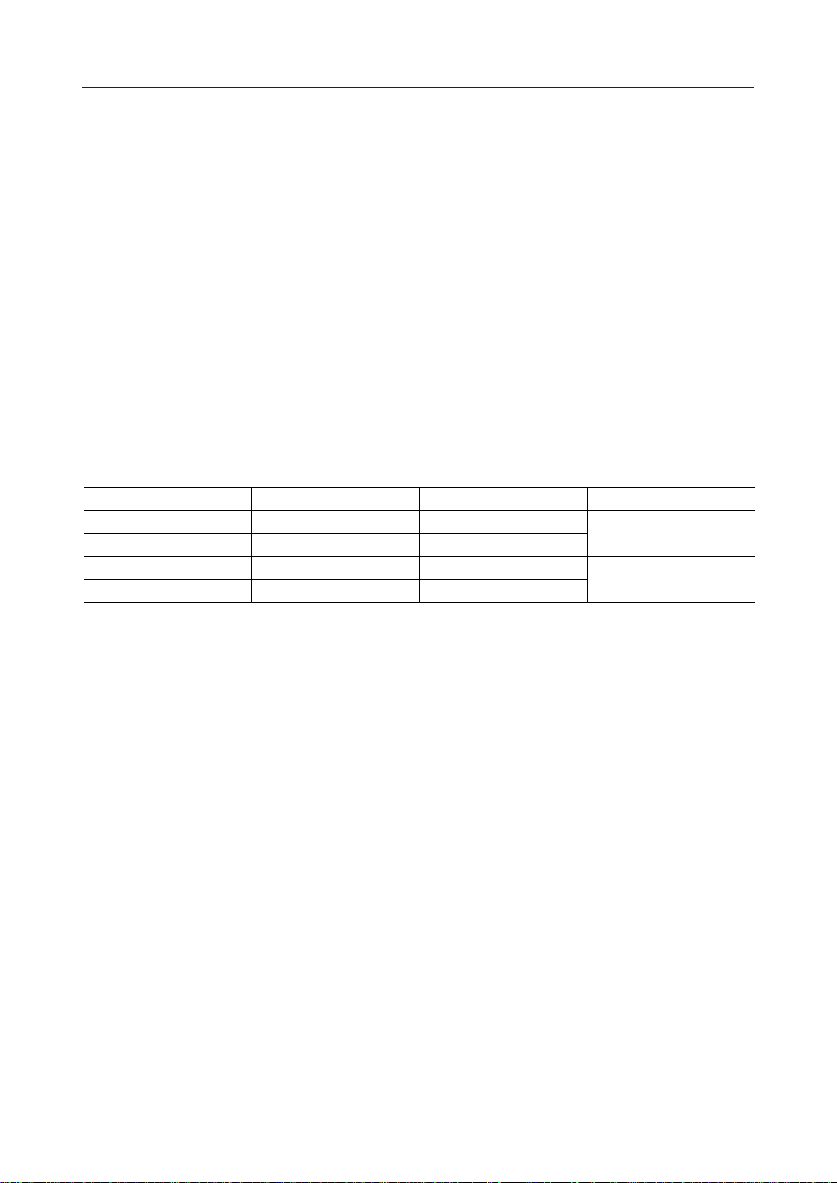
PRODUCT FAMILY
Family Cycle Time (Min.) Package
MSM5412222-25TS-K
MSM5412222-30TS-K
MSM5412222-25JS
MSM5412222-30JS
Access Time (Max.)
23 ns
25 ns
23 ns
25 ns
25 ns
400 mil 44-pin TSOP (II)
30 ns
25 ns
400 mil 40-pin SOJ
30 ns
2/15
Page 3
¡ Semiconductor MSM5412222
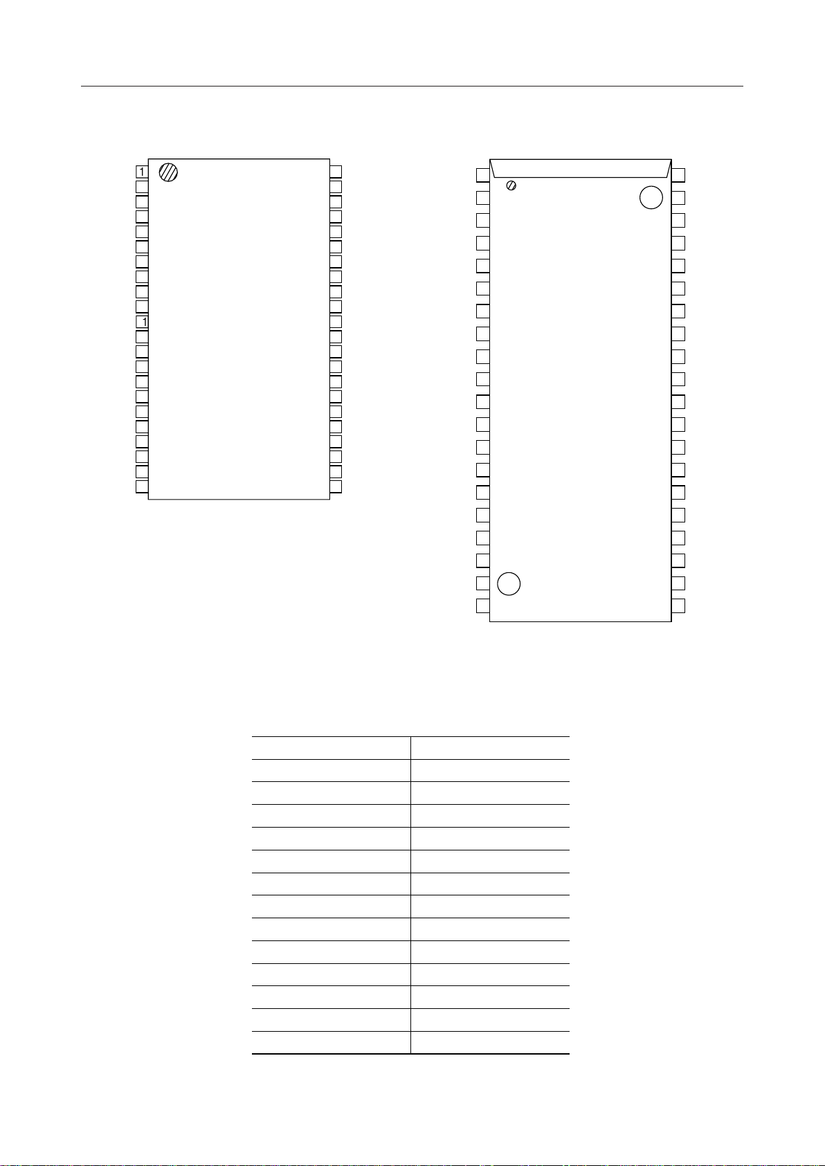
PIN CONFIGURATION (TOP VIEW)
1V
SS
2DIN11
3D
10
IN
4NC
5D
9
IN
6D
8
IN
7D
7
IN
8D
6
IN
9NC
10D
5
IN
11DIN4
12DIN3
13D
2
IN
14NC
15D
1
IN
16D
0
IN
17SWCK
18RSTW
19NC
20WE
21IE
22V
CC
44-Pin Plastic TSOP (II)
(K Type)
44 V
SS
43 D
OUT
42 D
OUT
41 NC
40 D
OUT
39 D
OUT
38 D
OUT
37 D
OUT
36 NC
35 D
OUT
34 D
OUT
33 D
OUT
32 D
OUT
31 V
SS
30 D
OUT
29 D
OUT
28 SRCK
27 RSTR
26 NC
25 RE
24 OE
23 V
CC
11
10
9
8
7
6
5
4
3
2
1
0
V
SS
DIN11
D
10
IN
D
IN
D
IN
D
IN
D
IN
D
IN
D
IN
DIN3
D
IN
D
IN
D
IN
SWCK
RSTW
WE
IE
NC
V
CC
1
2
3
4
5
9
6
8
7
7
8
6
9
5
10
4
11
12
2
13
1
14
0
15
16
17
18
19
20
40
39
38
37
36
35
34
33
32
31
30
29
28
27
26
25
24
23
22
21
V
SS
NCNC
D
OUT
D
OUT
D
OUT
D
OUT
D
OUT
D
OUT
D
OUT
D
OUT
D
OUT
D
OUT
D
OUT
D
OUT
SRCK
RSTR
RE
OE
V
SS
V
CC
11
10
9
8
7
6
5
4
3
2
1
0
Pin Name
SWCK
SRCK
WE
RE
IE
OE
RSTW
RSTR
0 - 11
D
IN
0 - 11
D
OUT
V
CC
V
SS
NC
40-Pin Plastic SOJ
Function
Serial Write Clock
Serial Read Clock
Write Enable
Read Enable
Input Enable
Output Enable
Write Reset Clock
Read Reset Clock
Data Input
Data Output
Power Supply (5 V)
Ground (0 V)
No Connection
Note: The same power supply voltage must be provided to every VCC pin, and the same GND
voltage level must be provided to every VSS pin.
3/15
Page 4
¡ Semiconductor MSM5412222
4/15
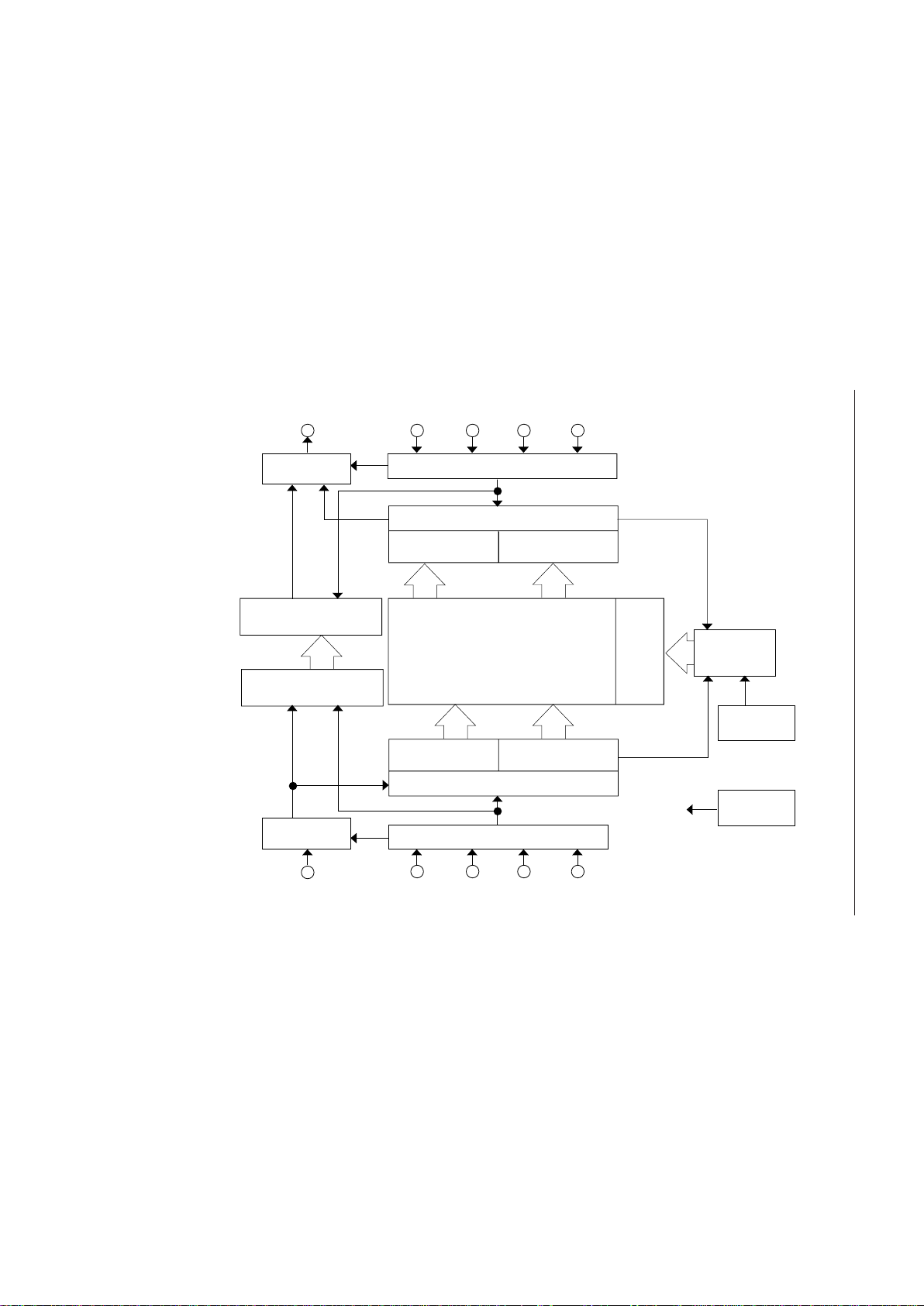
BLOCK DIAGRAM
D
OUT
(¥ 12)
Data-out
Buffer (¥ 12)
OE RE
RSTR SRCK
Serial
512 Word Serial Read Register (¥ 12)
Read Line Buffer
Low-Half (¥ 12)
Read Line Buffer
High-Half (¥ 12)
256 (¥ 12)
256K (¥ 12)
Memory
Array
X
Decoder
71 Word
Sub-Register (¥ 12)
Read/Write
and Refresh
Controller
Clock
Oscillator
Write Line Buffer
Low-Half (¥ 12)
Write Line Buffer
High-Half (¥ 12)
512 Word Serial Write Register (¥ 12)
Data-in
Buffer (¥ 12)
D
IN
(¥ 12)
Serial
IE WE RSTW
SWCK
71 Word
Sub-Register (¥ 12)
256 (¥ 12)
256 (¥ 12) 256 (¥ 12)
V
BB
Generator
Read Controller
Read Controller
Page 5

¡ Semiconductor MSM5412222
OPERATION
Write Operation
The write operation is controlled by three clocks, SWCK, RSTW, and WE. Write operation is
accomplished by cycling SWCK, and holding WE high after the write address pointer reset
operation or RSTW.
Each write operation, which begins after RSTW, must contain at least 80 active write cycles, i.e.
SWCK cycles while WE is high. To transfer the last data to the DRAM array, which at that time
is stored in the serial data registers attached to the DRAM array, an RSTW operation is required
after the last SWCK cycle.
Note that every write timing of MSM5412222 is delayed by one clock compared with read timings
for easy cascading without any interface delay devices.
Write Reset : RSTW
The first positive transition of SWCK after RSTW becomes high resets the write address counters
to zero. RSTW setup and hold times are referenced to the rising edge of SWCK. Because the write
reset function is solely controlled by the SWCK rising edge after the high level of RSTW, the states
of WE and IE are ignored in the write reset cycle.
Before RSTW may be brought high again for a further reset operation, it must be low for at least
two SWCK cycles.
Data Inputs : DIN0 - 11
Write Clock : SWCK
The SWCK latches the input data on chip when WE is high, and also increments the internal write
address pointer. Data-in setup time tDS, and hold time tDH are referenced to the rising edge of
SWCK.
Write Enable : WE
WE is used for data write enable/disable control. WE high level enables the input, and WE low
level disables the input and holds the internal write address pointer. There are no WE disable
time (low) and WE enable time (high) restrictions, because the MSM5412222 is in fully static
operation as long as the power is on. Note that WE setup and hold times are referenced to the
rising edge of SWCK.
Input Enable : IE
IE is used to enable/disable writing into memory. IE high level enables writing. The internal
write address pointer is always incremented by cycling SWCK regardless of the IE level. Note
that IE setup and hold times are referenced to the rising edge of SWCK.
5/15
Page 6

¡ Semiconductor MSM5412222
Read Operation
The read operation is controlled by three clocks, SRCK, RSTR, and RE. Read operation is
accomplished by cycling SRCK, and holding RE high after the read address pointer reset
operation or RSTR.
Each read operation, which begins after RSTR, must contain at least 80 active read cycles, i.e.
SRCK cycles while RE is high.
Read Reset : RSTR
The first positive transition of SRCK after RSTR becomes high resets the read address counters
to zero. RSTR setup and hold times are referenced to the rising edge of SRCK. Because the read
reset function is solely controlled by the SRCK rising edge after the high level of RSTR, the states
of RE and OE are ignored in the read reset cycle.
Before RSTR may be brought high again for a further reset operation, it must be low for at least
*two SRCK cycles.
Data Out : D
OUT
0 - 11
Read Clock : SRCK
Data is shifted out of the data registers. It is triggered by the rising edge of SRCK when RE is high
during a read operation. The SRCK input increments the internal read address pointer when RE
is high.
The three-state output buffer provides direct TTL compatibility ( no pullup resistor required).
Data out is the same polarity as data in. The output becomes valid after the access time interval
tAC that begins with the rising edge of SRCK. *There are no output valid time restriction on
MSM5412222.
Read Enable : RE
The function of RE is to gate of the SRCK clock for incrementing the read pointer. When RE is
high before the rising edge of SRCK, the read pointer is incremented. When RE is low, the read
pointer is not incremented. RE setup times (t
t
) are referenced to the rising edge of the SRCK clock.
RDSH
RENS
and t
) and RE hold times (t
RDSS
RENH
and
Output Enable : OE
OE is used to enable/disable the outputs. OE high level enables the outputs. The internal read
address pointer is always incremented by cycling SRCK regardless of the OE level. Note that OE
setup and hold times are referenced to the rising edge of SRCK.
6/15
Page 7

¡ Semiconductor MSM5412222
Power-up and Initialization
On power-up, the device is designed to begin proper operation after at least 100 ms after V
CC
has
stabilized to a value within the range of recommended operating conditions. After this 100 ms
stabilization interval, the following initialization sequence must be performed.
Because the read and write address counters are not valid after power-up, a minimum of 80
dummy write operations (SWCK cycles) and read operations (SRCK cycles) must be performed,
followed by an RSTW operation and an RSTR operation, to properly initialize the write and the
read address pointer. Dummy write cycles/RSTW and dummy read cycles/RSTR may occur
simultaneously.
If these dummy read and write operations start while VCC and/or the substrate voltage has not
stabilized, it is necessary to perform an RSTR operation plus a minimum of 80 SRCK cycles plus
another RSTR operation, and an RSTW operation plus a minimum of 80 SRCK cycles plus
another RSTW operation to properly initialize read and write address pointers.
Old/New Data Access
There must be a minimum delay of 600 SWCK cycles between writing into memory and reading
out from memory. If reading from the first field starts with an RSTR operation, before the start
of writing the second field (before the next RSTW operation), then the data just written will be
read out.
The start of reading out the first field of data may be delayed past the beginning of writing in the
second field of data for as many as 70 SWCK cycles. If the RSTR operation for the first field readout occurs less than 70 SWCK cycles after the RSTW operation for the second field write-in, then
the internal buffering of the device assures that the first field will still be read out. The first field
of data that is read out while the second field of data is written is called “old data”.
In order to read out “new data”, i.e., the second field written in, the delay between an RSTW
operation and an RSTR operation must be at least 600 SRCK cycles. If the delay between RSTW
and RSTR operations is more than 71 but less than 600 cycles, then the data read out will be
undetermined. It may be “old data” or “new” data, or a combination of old and new data. Such
a timing should be avoided.
Cascade Operation
The MSM5412222 is designed to allow easy cascading of multiple memory devices. This provides
higher storage depth, or a longer delay than can be achieved with only one memory device.
7/15
Page 8

¡ Semiconductor MSM5412222
ELECTRICAL CHARACTERISTICS
Absolute Maximum Ratings
Parameter Symbol Condition Rating
Input Output Voltage
Output Current
Power Dissipation
Operating Temperature
Storage Temperature
V
T
I
OS
P
D
T
opr
T
stg
Recommended Operating Conditions
Parameter Symbol Min. UnitTyp. Max.
Power Supply Voltage
Power Supply Voltage
Input High Voltage
Input Low Voltage
V
CC
V
SS
V
IH
V
IL
4.5
2.4
–1.0
DC Characteristics
Parameter Symbol Condition Min.
Input Leakage Current
Output Leakage Current
Output "H" Level Voltage
Output "L" Level Voltage
Operating Current
Standby Current
V
V
I
I
I
I
LO
OH
CC1
CC2
0 < VI < V
LI
OL
CC
Minimum Cycle Time, Output Open
at Ta = 25°C, V
SS
Ta = 25°C
Ta = 25°C
—
—
5.0
0
0
V
CC
0
+ 1, Other Pins Tested at V = 0 V
0 < VO < V
I
OH
I
OL
CC
= –1 mA
= 2 mA
-25
-30
Input Pin = V
IH
/ V
IL
–1.0 to 7.0
0 to 70
–55 to 150
–10
–10
2.4
—
—
—
—
50
1
5.5
0
V
+ 1
CC
0.8
Max. Unit
10
10
—
0.4
100
90
5
Unit
V
mA
W
°C
°C
V
V
V
V
mA
mA
V
V
mA
mA
Capacitance
Input Capacitance (D
Output Capacitance (D
Parameter Unit
, SWCK, SRCK, RSTW, RSTR, WE, RE, IE, OE)
IN
)
OUT
(Ta = 25°C, f = 1 MHz)
Symbol Max.
C
I
C
O
7
10
pF
pF
8/15
Page 9

¡ Semiconductor MSM5412222
AC Characteristics
Parameter Symbol Unit
Access Time from SRCK
D
Hold Time from SRCK
OUT
D
Enable Time from SRCK
OUT
SWCK "H" Pulse Width
SWCK "L" Pulse Width
Input Data Setup Time
Input Data Hold Time
WE Enable Setup Time
WE Enable Hold Time
WE Disable Setup Time
WE Disable Hold Time
IE Enable Setup Time
IE Enable Hold Time
IE Disable Setup Time
IE Disable Hold Time
WE "H" Pulse Width
WE "L" Pulse Width
IE "H" Pulse Width
IE "L" Pulse Width
RSTW Setup Time
RSTW Hold Time
SRCK "H" Pulse Width
SRCK "L" Pulse Width
RE Enable Setup Time
RE Enable Hold Time
RE Disable Setup Time
RE Disable Hold Time
OE Enable Setup Time
OE Enable Hold Time
OE Disable Setup Time
OE Disable Hold Time
Output Buffer Turn-off Delay Time from OE
RE "H" Pulse Width
RE "L" Pulse Width
OE "H" Pulse Width
OE "L" Pulse Width
RSTR Setup Time
RSTR Hold Time
SWCK Cycle Time
SRCK Cycle Time
Transition Time (Rise and Fall)
t
AC
t
DDCK
t
DECK
t
WSWH
t
WSWL
t
DS
t
DH
t
WENS
t
WENH
t
WDSS
t
WDSH
t
IENS
t
IENH
t
IDSS
t
IDSH
t
WWEH
t
WWEL
t
WIEH
t
WIEL
t
RSTWS
t
RSTWH
t
WSRH
t
WSRL
t
RENS
t
RENH
t
RDSS
t
RDSH
t
OENS
t
OENH
t
ODSS
t
ODSH
t
OEZ
t
WREH
t
WREL
t
WOEH
t
WOEL
t
RSTRS
t
RSTRH
t
SWC
t
SRC
t
T
MSM5412222-25
Min. Max.
—
6
6
9
10
2
4
0
3
0
3
0
3
0
3
5
5
5
5
0
3
9
10
0
3
0
3
0
3
0
3
17
5
5
5
5
0
3
25
25
3
23
—
23
—
—
—
—
—
—
—
—
—
—
—
—
—
—
—
—
—
—
—
—
—
—
—
—
—
—
—
—
—
—
—
—
—
—
—
—
—
30
(V
= 5 V ±10%, Ta = 0°C to 70°C)
CC
MSM5412222-30
Min. Max.
—
6
6
12
12
2
4
0
3
0
3
0
3
0
3
10
10
10
10
0
3
12
12
0
3
0
3
0
3
0
3
17
10
10
10
10
0
3
30
30
3
25
—
25
—
—
—
—
—
—
—
—
—
—
—
—
—
—
—
—
—
—
—
—
—
—
—
—
—
—
—
—
—
—
—
—
—
—
—
—
—
30
ns
ns
ns
ns
ns
ns
ns
ns
ns
ns
ns
ns
ns
ns
ns
ns
ns
ns
ns
ns
ns
ns
ns
ns
ns
ns
ns
ns
ns
ns
ns
ns
ns
ns
ns
ns
ns
ns
ns
ns
ns
9/15
Page 10

¡ Semiconductor MSM5412222
Notes: 1. Input signal reference levels for the parameter measurement are VIH = 3.0 V and V
= 0 V. The transition time tT is defined to be a transition time that signal transfers
between VIH = 3.0 V and VIL = 0 V.
2. AC measurements assume tT = 3 ns.
3. Read address must have more than a 600 address delay than write address in every
cycle when asynchronous read/write is performed.
4. Read must have more than a 600 address delay than write in order to read the data
written in a current series of write cycles which has been started at last write reset
cycle: this is called "new data read".
When read has less than a 70 address delay than write, the read data are the data
written in a previous series of write cycles which had been written before at last write
reset cycle: this is called "old data read".
5. When the read address delay is between more than 71 and less than 599, read data
will be undetermined. However, normal write is achieved in this address condition.
6. Outputs are measured with a load equivalent to 1 TTL load and 30 pF.
Output reference levels are VOH = 2.0 V and VOL = 0.8 V.
IL
10/15
Page 11

¡ Semiconductor MSM5412222
,
TIMING WAVEFORM
Write Cycle Timing (Write Reset)
n cycle 0 cycle 1 cycle 2 cycle
V
SWCK
RSTW
D
IN
t
WSWHtWSWL
t
t
t
T
t
DS
RSTWS
t
DH
n - 1 n
RSTWH
t
SWC
012
V
V
V
V
V
IH
IL
IH
IL
IH
IL
WE
IE
Write Cycle Timing (Write Enable)
n cycle Disable cycle Disable cycle n+1 cycle
SWCK
WE
D
t
WENH
t
WWEL
IN
n - 1 n
t
WDSH
t
WWEH
t
WDSS
t
WENS
n+1
V
V
V
V
V
V
V
V
V
V
IH
IL
IH
IL
IH
IL
IH
IL
IH
IL
V
IE
RSTW
IH
V
IL
V
IH
V
IL
11/15
Page 12

¡ Semiconductor MSM5412222
Write Cycle Timing (Input Enable)
n cycle n+1 cycle n+2 cycle n+3 cycle
V
SWCK
V
IH
IL
t
IENH
IE
t
WIEL
D
IN
n - 1 n n+3
WE
RSTW
Read Cycle Timing (Read Reset)
t
IDSH
t
WIEH
t
IDSS
t
IENS
V
V
V
V
V
V
V
V
IH
IL
IH
IL
IH
IL
IH
IL
SRCK
RSTR
D
OUT
RE
OE
n cycle 0 cycle 1 cycle 2 cycle
t
t
t
t
T
RSTRS
t
AC
RSTRH
WSRH
t
DDCK
t
SRC
t
WSRL
n - 1 n 0 1 2
V
V
V
V
V
V
V
V
V
V
IH
IL
IH
IL
OH
OL
IH
IL
IH
IL
12/15
Page 13

¡ Semiconductor MSM5412222
Read Cycle Timing (Read Enable)
n cycle disable cycle disable cycle n+1 cycle
V
SRCK
V
IH
IL
t
RENH
t
RDSH
RE
t
t
WREL
D
OUT
n - 1 n n+1
WREH
OE
RSTR
Read Cycle Timing (Output Enable)
t
RDSS
t
RENS
V
V
V
V
V
V
V
V
IH
IL
OH
OL
IH
IL
IH
IL
SRCK
OE
D
OUT
RE
RSTR
n cycle n+1 cycle n+2 cycle n+3 cycle
t
OENH
t
WOEN
n - 1 n n+3
t
ODSH
t
WOEH
Hi-Z
t
ODSS
t
OENS
t
DECK
V
V
V
V
V
V
V
V
V
V
IH
IL
IH
IL
OH
OL
IH
IL
IH
IL
13/15
Page 14

¡ Semiconductor MSM5412222
PACKAGE DIMENSIONS
(Unit : mm)
TSOPII44-P-400-0.80-K
Mirror finish
Package material
Lead frame material
Pin treatment
Solder plate thickness
Package weight (g)
Epoxy resin
42 alloy
Solder plating
5 mm or more
0.54 TYP.
Notes for Mounting the Surface Mount Type Package
The SOP, QFP, TSOP, SOJ, QFJ (PLCC), SHP and BGA are surface mount type packages, which
are very susceptible to heat in reflow mounting and humidity absorbed in storage.
Therefore, before you perform reflow mounting, contact Oki’s responsible sales person for the
product name, package name, pin number, package code and desired mounting conditions
(reflow method, temperature and times).
14/15
Page 15

¡ Semiconductor MSM5412222
(Unit : mm)
SOJ40-P-400-1.27
Mirror finish
Package material
Lead frame material
Pin treatment
Solder plate thickness
Package weight (g)
Epoxy resin
42 alloy
Solder plating
5 mm or more
1.70 TYP.
Notes for Mounting the Surface Mount Type Package
The SOP, QFP, TSOP, SOJ, QFJ (PLCC), SHP and BGA are surface mount type packages, which
are very susceptible to heat in reflow mounting and humidity absorbed in storage.
Therefore, before you perform reflow mounting, contact Oki’s responsible sales person for the
product name, package name, pin number, package code and desired mounting conditions
(reflow method, temperature and times).
15/15
 Loading...