

Page 1

E2B0020-27-Y2
¡ Semiconductor
This version: Nov. 1997
Previous version: Mar. 1996
MSM5299A¡ Semiconductor
MSM5299A
80-DOT LCD SEGMENT DRIVER
GENERAL DESCRIPTION
The MSM5299A is a dot matrix LCD segment driver LSI which is fabricated using CMOS low
power metal gate technology. This LSI consists of an 80-bit bidirectional shift register, 80-bit
latch, 80-bit level shifter and 80-bit 4-level driver.
It receives the display data, which is transferred in 4-bit parallel from a microcomputer or LCD
controller LSI such as MSM6255, then outputs the LCD driving waveform to the LCD.
FEATURES
• Supply voltage : 4.5 to 5.5V
• LCD driving voltage : 8 to 28V
• Applicable LCD duty : 1/64 to 1/256
• LCD Output : 80
• The 4-bit parallel data processing has improved the transfer speed to 1/4 that of the
conventional serial transfer, thereby achieving low power consumption
• Can be interfaced with the LCD controller LSI MSM6255
• Applicable common diriver : MSM5298A (68 outputs)
• Package options:
100-pin plastic QFP (QFP100-P-1420-0.65-K) (Product name : MSM5299AGS-K)
100-pin plastic QFP (QFP100-P-1420-0.65-BK) (Product name : MSM5299AGS-BK)
1/11
Page 2
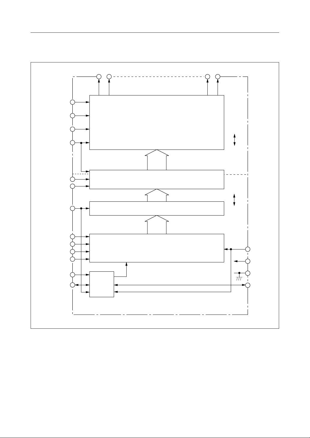
BLOCK DIAGRAM
MSM5299A¡ Semiconductor
V
V
V
V
DF
DISP OFF
LOAD
D
D
D
D
CP
EL
O1O
2
1
3
O79O
80
80-Bit 4-Level Driver
V
4
EE
DD
V
EE
80-Bit Level Shifter
V
DD
80-Bit Latch (Edge trigger D-F/F)
0
1
2
3
4 x 20-Bit Bidirectional Shift Register
SHIFT CP
V
SS
SHL
V
DD
V
SS
Control
Circuit
ER
2/11
Page 3
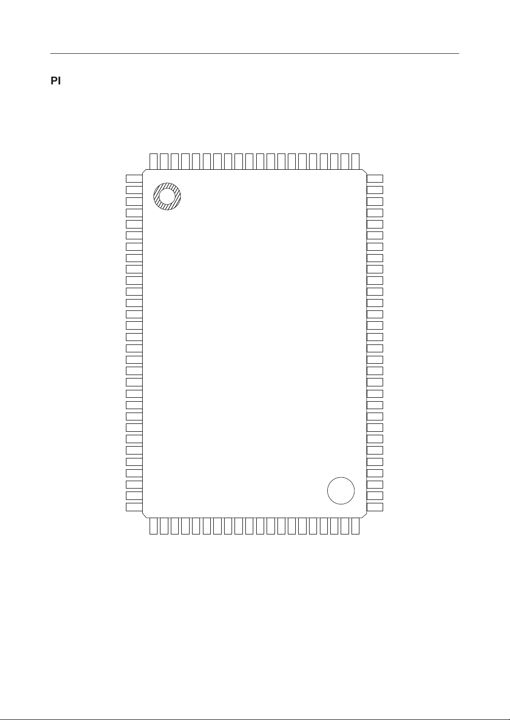
PIN CONFIGURATION (TOP VIEW)
MSM5299A¡ Semiconductor
50
9998979695949392919089
100
1
O
51
O
2
52
O
3
53
O
4
54
O
5
55
O
6
56
O
7
57
8
O
58
9
O
59
O
10
60
11
O
61
12
O
62
13
O
63
O
14
64
O
15
65
16
O
66
17
O
67
18
O
68
O
19
69
O
20
70
21
O
71
22
O
72
23
O
73
O
24
74
O
25 56
75
O
26
76
O
27
77
O
28
78
O
29
79
O
30
80
46
O48O49O
O47O
43
45
42
O
O
O44O
O41O40O39O
38
88
O37O36O
878685
35
34
O
O33O32O
838281
31
80
O
30
O
79
29
78
O
28
O
77
27
O
76
26
75
O
25
O
74
24
O
73
23
O
72
22
O
71
21
O
70
20
69
O
19
O
68
18
67
O
17
O
66
16
O
65
15
64
O
14
O
63
13
62
O
12
O
61
11
O
60
10
59
O
9
O
58
8
57
O
7
O
6
55
O
5
54
O
4
53
O
3
52
O
2
51
O
1
31323334353637383940414243
ER
NC
EE
V
V4V3V
1
NC
DD
DF
V
SHL
DISPOFF
444546
SS
D2
D1
D3
V
D0
47 84
CP
484950
NC
LOAD
EL
NC : No connection
100-Pin Plastic QFP
Note: The abbreviated part number "M5299A" is imprinted on the package surface.
3/11
Page 4
ABSOLUTE MAXIMUM RATINGS
Parameter
Supply Voltage (1)
Supply Voltage (2)
Input Voltage
Storage Temperature
*1 V
DD≥V1>V3>V4>VEE
Symbol Condition Rating Unit
V
DD
V
LCD
V
I
STG
Ta = 25°C, V
RECOMMENDED OPERATING CONDITIONS
Parameter
Supply Voltage (1)
Supply Voltage (2)
Operating Temperature
Symbol Condition Range Unit
V
DD
V
LCD
T
op
V
Ta = 25°C
DD
Ta = 25°C
—
—
– V
DD
EE
—
– V
MSM5299A¡ Semiconductor
=0V)
(V
SS
–0.3 to +6
*1
EE
0 to 30
–0.3 to V
DD
+0.3
–55 to +150T
4.5 to 5.5
*1
8 to 28
–20 to +85
V
V
V
°C
(VSS=0V)
V
V
°C
*1 V
DD≥V1>V3>V4>VEE
4/11
Page 5

ELECTRICAL CHARACTERISTICS
MSM5299A¡ Semiconductor
DC Characteristics
(VDD = 5V ± 10%, Ta = –20 to +85°C)
Parameter Symbol Condition Min. Typ. Max. Unit
"H" Input Voltage V
"L" Input Voltage V
"H" Input Current V
"H" Output Voltage V
"L" Output Voltage V
ON Resistance R
Stand-by Current
I
DDSBY
Supply Current (1) I
Supply Current (2) I
V
OH
OL
ON
DD1
IH
IL
IH
IL
= –0.2mA, VDD = 4.5V
O
= 0.2mA, VDD = 4.5V
O
V
V
DD
V
N
= 1MHz, V
f
CP
V
DD
=1MHz, V
f
CP
V
DD
= 1MHz, V
f
V
CP
V
DD
23V
–
=
EE
0.25V,
DD
26
V,
DD
26V,
DD
26V,
V
DD
= 5.5V
No load
= 5.5V
No load
= 5.5V
No load
= 4.5V
V
–
=
O
V
–
=
EE
V
–
=
EE
V
–
=
EE
*3
*5
*6
*7
0.8V
V
DD
SS
—VDDV*1 —
— 0.2V
——1mA*1 VIH = VDD, VDD = 5.5V
——–1mA*1 VIL = 0V, VDD = 5.5V"H" Input Current
V
– 0.4 — — V*2 I
DD
— — 0.4 V*2 I
—24kW*4
— — 200 mA
——3mA
— — ±100 mA
DD
V*1 —
Input Capacitance C
I
*1 Applicable to LOAD, CP, D0 - D3, EL, ER, SHL, DF, DISP OFF
*2 Applicable to EL, ER.
*3 VN = VDD to V
EE, V4
15
13
= (VDD – VEE), V3 = (VDD – VEE), V1 = V
2
15
*4 Applicable to O1 to O80.
*5 Display data 1010
......
fDF = 40 Hz, Current from VDD to VSS when the display data is not
processing.
*6 Display data 1010
......
fDF = 40 Hz, Current from VDD to VSS when the display data is
processing.
*7 Display data 1010
......
fDF = 40 Hz, Current on V1, V3 and V4.
—5—pFf = 1MHz
DD
5/11
Page 6

Switching Characteristics
Parameter
Clock Frequency
Clock, Load Pulse Width
Clock Pulse Rise/Fall Time
Data Set-up Time
Data Hold Time
Load Set-up Time
Load Æ Clock Time
MSM5299A¡ Semiconductor
(VDD = 5V ± 10%, Ta = –20 to +75°C, CL = 15pF)
Symbol Condition Min. Typ. Max. Unit
f
CP
t
W
tr, t
t
DSU
t
DHD
t
LSU
t
LC
DUTY=50% —
—
f
—
—
—
—
—
100
—
50
80
90
200
—
—
—
—
—
—
—
3.4
—
50
—
—
—
—
MHz
ns
ns
ns
ns
ns
ns
Propagation Delay Time
ER, EL Set-up Time
CP
- D
D
0
3
LOAD
CP
0.8V
DD
t
PHL
t
ESU
t
t
DSU
0.8V
0.2V
0.2V
DD
DD
DD
DD
f
0.2V
t
0.8V
0.2V
t
DHD
r
t
W
0.8V
DD
DD
0.8V
DD
t
DD
W
t
LSU
t
W
—
—
t
r
0.2V
0.8V
t
f
0.8V
DD
0.2V
DD
70
—
DD
DD
t
W
t
LC
1 2 19 20
0.8V
0.2V
—
—
DD
DD
224
—
0.8V
ns
ns
DD
LOAD
ER, EL (Output)
EL, ER (Input)
t
0.2V
PHL
DD
t
ESU
0.2V
DD
6/11
Page 7

FUNCTIONAL DESCRIPTION
Pin Functional Description
• ER, EL
MSM5299A¡ Semiconductor
Pin Input/Output
ER
EL
EL
ER
Input
Output
Input
Output
SHL
L
H
Input pin to ENABLE F/F of MSM5299A.
Output pin of ENABLE F/F. EL is connected to next MSM5299A's
ER when MSM5299As are connected in series (cascade
connection).
Input pin to ENABLE F/F of MSM5299A.
Output pin of ENABLE F/F. ER is connected to next MSM5299A's
EL when MSM5299As are connected in series (cascade
Description
connection).
When single MSM5299A is used, ER (EL) should be set at "L" level.
When a cascade connection is required, set the ER (EL) pin of the first MSM5299A at "L" level
and connect the EL (ER) pin of the first MSM5299A to the ER (EL) pin of the second MSM5299A,
then connect the EL ( ER) pin of the second MSM5299A to the ER (EL) pin of the third MSM5299A.
•CP
Clock pulse input pin for the 4-bit parallel shift register. The data is shifted to 4 ¥ 20-bit shift
register at the falling edge of the clock pulse. The clock pulse is activated when the ENABLE
F/F is set and is deactivated when the ENABLE F/F is not set.
• SHL
Input pin to switch the input or output of pins ER and EL, and the shift direction of the 4-bit
parallel bidirectional shift register.
The shift direction of the 4-bit parallel data, the correspondence of the data D0 to D3 to the
driver outputs O1 to O80, and the input and output state of pins ER and EL are shown in the
table below.
SHL
L
H
ER
Input
Output
EL
Output
Input
Shift direction
D
0
D
1
D
2
D
3
D
0
D
1
D
2
D
3
O
1
O
2
O
3
O
4
O
80
O
79
O
78
O
77
end data
O
5
O
6
O
7
O
8
O
76
O
75
O
74
O
73
O
77
O
78
O
79
O
80
O
4
O
3
O
2
O
1
start data
7/11
Page 8

MSM5299A¡ Semiconductor
•D0, D1, D2, D
3
Display data input pins for 4 ¥ 20-bit shift register. The display data is clocked into the shift
register at the falling edge of the clock pulse. The combinations of D0 to D3 level, DF signal
level, display data output level and the display on the LCD panel are described on the table
below.
to D
D
0
L
H
L
H
DF Display data output level Display on the LCD
3
L
L
H
H
Nonselect level (V
Select level (V
Nonselect level (V
Select level (V
)
3
)
1
)
4
)
EE
OFF
ON
OFF
ON
• LOAD
The signal for latching the shift register contents is input to this pin. The display data stored
in the shift register is latched at the falling edge of the load pulse.
•DF
Synchronous signal input pin for alternate signal for LCD driving.
•VDD, V
SS
Supply voltage pins, VDD should be 4.5 to 5.5V. VSS is a ground pin (VSS = 0V)
•V1, V3, V4, V
EE
Bias supply voltage pin to drive the LCD. Use an external bias voltage supply for driving the
LCD.
8/11
Page 9

MSM5299A¡ Semiconductor
•O1 - O
80
Display data output pins, which correspond to the respective latch contents. One of V1, V3,
V4 and VEE is selected as a display driving voltage source according to the combination of the
latched data level and DF signal. Refer to the Truth Table.
The outputs O1 to O80 are connected to the segment side of the LCD panel.
• DISP OFF
Input pin to control outputs of O1 to O80. V1 level is output from O1 to O80 pins during "L"
level input. Refer to the Truth Table.
Truth Table
DF
H
H
X
Latched data DISP OFF LCD driver output (O
L
L
L
H
L
H
X
H
H
H
H
L
V
3
V
1
V
4
V
EE
V
1
- O80)
1
X : Don't care
NOTES ON USE
Note the following when turning power on and off:
The LCD drivers of this IC require a high voltage. For this reason, if a high voltage is applied to
the LCD drivers with the logic power supply floating, excess current flows. This may damage
the IC. Be sure to carry out the following power-on and power-off sequences:
When turning power on:
First VDD ON, next VEE, V4, V3, V1 ON. Or both ON at the same time.
When turning power off:
First VEE, V4, V3, V1 OFF, next VDD OFF. Or both OFF at the same time.
9/11
Page 10

PACKAGE DIMENSIONS
QFP100-P-1420-0.65-K
Mirror finish
MSM5299A¡ Semiconductor
(Unit : mm)
Package material
Lead frame material
Pin treatment
Solder plate thickness
Package weight (g)
Epoxy resin
42 alloy
Solder plating
5 mm or more
1.29 TYP.
Notes for Mounting the Surface Mount Type Package
The SOP, QFP, TSOP, SOJ, QFJ (PLCC), SHP and BGA are surface mount type packages, which
are very susceptible to heat in reflow mounting and humidity absorbed in storage.
Therefore, before you perform reflow mounting, contact Oki’s responsible sales person for the
product name, package name, pin number, package code and desired mounting conditions
(reflow method, temperature and times).
10/11
Page 11

QFP100-P-1420-0.65-BK
Mirror finish
MSM5299A¡ Semiconductor
(Unit : mm)
Package material
Lead frame material
Pin treatment
Solder plate thickness
Package weight (g)
Epoxy resin
42 alloy
Solder plating
5 mm or more
1.29 TYP.
Notes for Mounting the Surface Mount Type Package
The SOP, QFP, TSOP, SOJ, QFJ (PLCC), SHP and BGA are surface mount type packages, which
are very susceptible to heat in reflow mounting and humidity absorbed in storage.
Therefore, before you perform reflow mounting, contact Oki’s responsible sales person for the
product name, package name, pin number, package code and desired mounting conditions
(reflow method, temperature and times).
11/11
 Loading...